WO2022038895A1 - 固体撮像素子、および、撮像装置 - Google Patents
固体撮像素子、および、撮像装置 Download PDFInfo
- Publication number
- WO2022038895A1 WO2022038895A1 PCT/JP2021/024083 JP2021024083W WO2022038895A1 WO 2022038895 A1 WO2022038895 A1 WO 2022038895A1 JP 2021024083 W JP2021024083 W JP 2021024083W WO 2022038895 A1 WO2022038895 A1 WO 2022038895A1
- Authority
- WO
- WIPO (PCT)
- Prior art keywords
- transistor
- input
- potential
- drain
- output
- Prior art date
- Legal status (The legal status is an assumption and is not a legal conclusion. Google has not performed a legal analysis and makes no representation as to the accuracy of the status listed.)
- Ceased
Links
Images




















Classifications
-
- H—ELECTRICITY
- H04—ELECTRIC COMMUNICATION TECHNIQUE
- H04N—PICTORIAL COMMUNICATION, e.g. TELEVISION
- H04N25/00—Circuitry of solid-state image sensors [SSIS]; Control thereof
- H04N25/70—SSIS architectures; Circuits associated therewith
- H04N25/709—Circuitry for control of the power supply
-
- H—ELECTRICITY
- H04—ELECTRIC COMMUNICATION TECHNIQUE
- H04N—PICTORIAL COMMUNICATION, e.g. TELEVISION
- H04N25/00—Circuitry of solid-state image sensors [SSIS]; Control thereof
- H04N25/70—SSIS architectures; Circuits associated therewith
- H04N25/76—Addressed sensors, e.g. MOS or CMOS sensors
-
- H—ELECTRICITY
- H03—ELECTRONIC CIRCUITRY
- H03K—PULSE TECHNIQUE
- H03K5/00—Manipulating of pulses not covered by one of the other main groups of this subclass
- H03K5/22—Circuits having more than one input and one output for comparing pulses or pulse trains with each other according to input signal characteristics, e.g. slope, integral
- H03K5/24—Circuits having more than one input and one output for comparing pulses or pulse trains with each other according to input signal characteristics, e.g. slope, integral the characteristic being amplitude
- H03K5/2472—Circuits having more than one input and one output for comparing pulses or pulse trains with each other according to input signal characteristics, e.g. slope, integral the characteristic being amplitude using field effect transistors
-
- H—ELECTRICITY
- H03—ELECTRONIC CIRCUITRY
- H03M—CODING; DECODING; CODE CONVERSION IN GENERAL
- H03M1/00—Analogue/digital conversion; Digital/analogue conversion
- H03M1/12—Analogue/digital converters
- H03M1/50—Analogue/digital converters with intermediate conversion to time interval
- H03M1/56—Input signal compared with linear ramp
-
- H—ELECTRICITY
- H04—ELECTRIC COMMUNICATION TECHNIQUE
- H04N—PICTORIAL COMMUNICATION, e.g. TELEVISION
- H04N25/00—Circuitry of solid-state image sensors [SSIS]; Control thereof
- H04N25/70—SSIS architectures; Circuits associated therewith
- H04N25/76—Addressed sensors, e.g. MOS or CMOS sensors
- H04N25/77—Pixel circuitry, e.g. memories, A/D converters, pixel amplifiers, shared circuits or shared components
-
- H—ELECTRICITY
- H04—ELECTRIC COMMUNICATION TECHNIQUE
- H04N—PICTORIAL COMMUNICATION, e.g. TELEVISION
- H04N25/00—Circuitry of solid-state image sensors [SSIS]; Control thereof
- H04N25/70—SSIS architectures; Circuits associated therewith
- H04N25/76—Addressed sensors, e.g. MOS or CMOS sensors
- H04N25/78—Readout circuits for addressed sensors, e.g. output amplifiers or A/D converters
-
- H—ELECTRICITY
- H03—ELECTRONIC CIRCUITRY
- H03M—CODING; DECODING; CODE CONVERSION IN GENERAL
- H03M1/00—Analogue/digital conversion; Digital/analogue conversion
- H03M1/12—Analogue/digital converters
- H03M1/1205—Multiplexed conversion systems
- H03M1/123—Simultaneous, i.e. using one converter per channel but with common control or reference circuits for multiple converters
-
- H—ELECTRICITY
- H03—ELECTRONIC CIRCUITRY
- H03M—CODING; DECODING; CODE CONVERSION IN GENERAL
- H03M1/00—Analogue/digital conversion; Digital/analogue conversion
- H03M1/12—Analogue/digital converters
- H03M1/124—Sampling or signal conditioning arrangements specially adapted for A/D converters
- H03M1/129—Means for adapting the input signal to the range the converter can handle, e.g. limiting, pre-scaling ; Out-of-range indication
- H03M1/1295—Clamping, i.e. adjusting the DC level of the input signal to a predetermined value
-
- H—ELECTRICITY
- H10—SEMICONDUCTOR DEVICES; ELECTRIC SOLID-STATE DEVICES NOT OTHERWISE PROVIDED FOR
- H10F—INORGANIC SEMICONDUCTOR DEVICES SENSITIVE TO INFRARED RADIATION, LIGHT, ELECTROMAGNETIC RADIATION OF SHORTER WAVELENGTH OR CORPUSCULAR RADIATION
- H10F39/00—Integrated devices, or assemblies of multiple devices, comprising at least one element covered by group H10F30/00, e.g. radiation detectors comprising photodiode arrays
- H10F39/80—Constructional details of image sensors
- H10F39/809—Constructional details of image sensors of hybrid image sensors
Definitions
- This technology relates to a solid-state image sensor. More specifically, the present invention relates to a solid-state image pickup device provided with a comparator and a counter, and an image pickup device.
- a single-slope type ADC Analog to Digital Converter
- AD Analog to Digital
- This single-slope ADC is generally composed of a comparator and a counter that counts based on the comparison result of the comparator.
- a solid-state image sensor in which a pMOS (p-channel Metal-Oxide-Semiconductor) transistor, a current source, and a logic gate (inverter, etc.) are arranged in this comparator has been proposed (see, for example, Patent Document 1). ..
- This pMOS transistor compares the pixel signal from the pixel circuit with the reference signal, and outputs the comparison result from the drain via the inverter. This comparison result is initialized to a low level by inputting a high level reference voltage immediately before the start of counting of the counter.
- the current of the pixel circuit is shared by the comparator, so that the power consumption is reduced as compared with the configuration in which the current source is also provided in the comparator separately from the pixel circuit.
- This technology was created in view of this situation, and aims to improve the responsiveness of the comparator in a solid-state image sensor equipped with a comparator for each column.
- the present technology has been made to solve the above-mentioned problems, and the first aspect thereof is whether or not the input potential input to the source and the predetermined reference potential input to the gate substantially match.
- An input transistor that outputs a potential within the range from one to the other of the pair of output potentials from the drain, a first current source that supplies a constant current, a source of the input transistor, and the first one.
- It is a solid-state imaging device including a first cutoff switch that disconnects the drain of a transistor and connects the connection node and the drain of the input transistor outside the predetermined period. This has the effect of improving responsiveness.
- the first cutoff switch may include an N-type transistor and a P-type transistor connected in parallel between the drain of the input transistor and the first current source. ..
- the comparison operation can be performed without being affected by the cutoff switch.
- the first cutoff switch may include an N-type transistor. This has the effect of reducing the number of transistors.
- a first output transistor that outputs a potential within the range from a low predetermined potential to the input potential from the drain, and an output-side short-circuit switch that short-circuits the source and drain of the first output transistor within the predetermined period. Further may be provided. This has the effect of improving responsiveness.
- the auto-zero transistor for connecting the gate and the drain of the input transistor is further provided within the auto-zero period before the predetermined period, and the output-side short-circuit switch is within the auto-zero period and the above.
- the source and drain of the first output transistor may be short-circuited within a predetermined period. This has the effect of suppressing oscillation during the auto-zero period.
- the output side short-circuit switch may include an N-type transistor and a P-type transistor connected in parallel between the source and drain of the first output transistor. This has the effect that the source and drain of the first output transistor are short-circuited when the level of the comparison result is about the middle of the power supply potential.
- the output side short-circuit switch may include an N-type transistor. This has the effect of reducing the number of transistors.
- the output side short-circuit switch may include a P-type transistor. This has the effect of reducing the number of transistors.
- the above is based on whether or not the difference between the input potential input to the source and the drain of the first output transistor input to the gate exceeds a predetermined threshold voltage.
- a second output transistor that outputs a voltage within the range from the predetermined potential to the input potential from the drain may be further provided. As a result, the gain of the comparator is increased, so that the linearity is improved.
- an input side short-circuit switch for short-circuiting the drain and the source of the input transistor may be further provided within the predetermined period. This has the effect of suppressing deterioration of characteristics.
- a level shift circuit that outputs an output signal of a pair of shift potentials having a potential difference larger than the predetermined potential and the input potential based on the potential of the drain of the first output transistor, and the above. Further, a logic gate for determining whether or not the output signal is higher than a predetermined threshold value between the pair of shift potentials and outputting the determination result may be provided. This has the effect of improving the degree of freedom in design.
- one of the pair of shift potentials is a power supply potential higher than the input potential
- the other is a reference potential lower than the predetermined potential
- the level shift circuit is the input potential.
- An N-type transistor in which a gate is connected to the vertical signal line of the above and a source is connected to the dray of the first output transistor, and a power supply-side precharge transistor that initializes the drain potential of the N-type transistor to the power supply potential.
- a P-type transistor in which a gate is connected to the drain of the N-type transistor and a drain is connected to the logic gate
- a reference-side precharge transistor that initializes the drain potential of the P-type transistor to the reference potential. May be provided. This has the effect of expanding the voltage circuit with the four transistors.
- the first output transistor that outputs a potential in the range from a low predetermined potential to the input potential from the drain, the second current source that supplies a constant current, and the first output transistor before the start timing of settling of the reference potential.
- a second cutoff switch that disconnects the drain of the output transistor 1 from the second current source and connects the drain of the first output transistor and the second current source for a certain period from the start timing.
- the clamp transistor to which the drain is connected to the second current source, the source of the first output transistor and the source of the clamp transistor are connected before the start timing, and the source of the clamp transistor is connected for a certain period from the start timing. Further, a control switch for disconnecting the source of the first output transistor from the source of the clamp transistor may be further provided. This has the effect of suppressing kickback.
- a level shift circuit that outputs an output signal of a pair of shift potentials having a potential difference larger than the predetermined potential and the input potential based on the potentials of the connection nodes of the control switch and the clamp transistor is provided. Further may be provided. This has the effect of improving the degree of freedom in design.
- an input capacitance switching circuit for switching the number of input capacitances connected in parallel to the gate of the input transistor may be further provided. This has the effect of reducing noise.
- the second aspect of the present technology is an input in which a drain potential corresponding to the input potential is output from the drain when the input potential input to the source and a predetermined reference potential input to the gate substantially match.
- the third aspect of the present technology is an input transistor that outputs a predetermined clamp potential from the drain when the input potential input to the source and a predetermined reference potential input to the gate substantially match.
- a solid-state imaging device including an input-side short-circuit switch that short-circuits the source and drain of the input transistor within a predetermined period for initializing the drain potential to a higher level than the clamp potential. This has the effect of improving responsiveness.
- the fourth aspect of the present technology is the range from one to the other of the pair of output potentials based on whether or not the input potential input to the source and the predetermined reference potential input to the gate substantially match.
- An input transistor that outputs the potential inside from the drain, a current source that supplies a predetermined constant current, a capacitance inserted between the source of the input transistor and the current source, and a connection between the capacitance and the current source.
- the drain of the input transistor is disconnected from the connection node within a predetermined period for initializing the node to the lower of the pair of output potentials, and the connection node and the drain of the input transistor are connected outside the predetermined period.
- It is an image pickup apparatus provided with a cutoff switch to be turned off and a counter for counting a count value over a period until the potential of the connection node is inverted. This has the effect of improving responsiveness.
- a fifth aspect of the present technology is a transistor comprising a vertical signal line connected to a pixel, a source connected to the vertical signal line, and a gate that receives a signal based on a predetermined reference potential.
- a sixth aspect of the present technology is a first transistor comprising a vertical signal line connected to a pixel, a source connected to the vertical signal line, and a gate that receives a signal based on a predetermined reference potential.
- a second transistor comprising a current source to supply a constant current, a source connected to the vertical signal line, and a gate connected to the current source, and the source and drain of the second transistor. It is a solid-state imaging device including a switch connected to and.
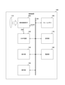
- FIG. 1 is a block diagram showing a configuration example of an image pickup apparatus 100 according to a first embodiment of the present technology.
- the image pickup device 100 is a device for capturing image data, and includes an optical unit 110, a solid-state image pickup element 200, and a DSP (Digital Signal Processing) circuit 120. Further, the image pickup apparatus 100 includes a display unit 130, an operation unit 140, a bus 150, a frame memory 160, a storage unit 170, and a power supply unit 180.
- a camera mounted on a smartphone, an in-vehicle camera, or the like is assumed.
- the optical unit 110 collects the light from the subject and guides it to the solid-state image sensor 200.
- the solid-state image sensor 200 generates image data by photoelectric conversion.
- the solid-state image sensor 200 supplies the generated image data to the DSP circuit 120 via the signal line 209.
- the DSP circuit 120 executes predetermined signal processing on the image data.
- the DSP circuit 120 outputs the processed image data to the frame memory 160 or the like via the bus 150.
- the display unit 130 displays image data.
- a liquid crystal panel or an organic EL (ElectroLuminescence) panel is assumed.
- the operation unit 140 generates an operation signal according to the operation of the user.
- the bus 150 is a common route for the optical unit 110, the solid-state image sensor 200, the DSP circuit 120, the display unit 130, the operation unit 140, the frame memory 160, the storage unit 170, and the power supply unit 180 to exchange data with each other.
- the frame memory 160 holds image data.
- the storage unit 170 stores various data such as image data.
- the power supply unit 180 supplies power to the solid-state image sensor 200, the DSP circuit 120, the display unit 130, and the like.
- FIG. 2 is a diagram showing an example of a laminated structure of the solid-state image pickup device 200 according to the first embodiment of the present technology.
- the solid-state image sensor 200 includes a circuit chip 202 and a light receiving chip 201 laminated on the circuit chip 202. These chips are electrically connected via a connection such as a via. In addition to vias, it can also be connected by Cu-Cu bonding or bumps.
- FIG. 3 is a block diagram showing a configuration example of the solid-state image sensor 200 according to the first embodiment of the present technology.
- the solid-state image sensor 200 includes a vertical scanning circuit 210, a timing control unit 220, a DAC (Digital to Analog Converter) 230, a pixel array unit 240, a column signal processing unit 260, and a horizontal scanning circuit 270.
- a plurality of pixel circuits 250 are arranged in a two-dimensional grid pattern in the pixel array unit 240.
- the pixel array unit 240 is arranged on the light receiving chip 201, for example, and the remaining circuits are arranged on the circuit chip 202.
- the circuit arranged on each chip is not limited to the circuit illustrated in the figure.
- the vertical scanning circuit 210 sequentially selects and drives the rows in the pixel array unit 240.
- the timing control unit 220 controls the operation timing of the vertical scanning circuit 210, the DAC 230, the column signal processing unit 260, and the horizontal scanning circuit 270 in synchronization with the vertical synchronization signal VSYNC.
- the DAC 230 generates a sawtooth wave lamp signal and supplies it to the column signal processing unit 260 as a reference signal.
- the pixel circuit 250 generates an analog pixel signal by photoelectric conversion under the control of the vertical scanning circuit 210.
- the pixel circuit 250 in each row outputs a pixel signal to the column signal processing unit 260 via a vertical signal line (not shown).
- An ADC (not shown) is arranged in each column of the pixel circuit 250 in the column signal processing unit 260.
- Each of the ADCs converts the pixel signal of the corresponding column into a digital signal and outputs it to the DSP circuit 120 under the control of the horizontal scanning circuit 270.
- the horizontal scanning circuit 270 controls the column signal processing unit 260 to output digital signals in order.
- FIG. 4 is a circuit diagram showing a configuration example of the pixel circuit 250 according to the first embodiment of the present technology.
- the pixel circuit 250 includes a photoelectric conversion element 251, a transfer transistor 252, a reset transistor 253, a floating diffusion layer 254, an amplification transistor 255, and a selection transistor 256. Further, in the pixel array unit 240, vertical signal lines 259 are wired for each row along the vertical direction.
- the photoelectric conversion element 251 photoelectrically converts incident light to generate an electric charge.
- the transfer transistor 252 transfers an electric charge from the photoelectric conversion element 251 to the stray diffusion layer 254 according to the drive signal TRG from the vertical scanning circuit 210.
- the reset transistor 253 is initialized by extracting electric charges from the stray diffusion layer 254 according to the drive signal RST from the vertical scanning circuit 210.
- the floating diffusion layer 254 accumulates electric charges and generates a voltage according to the amount of electric charges.
- the amplification transistor 255 amplifies the voltage of the stray diffusion layer 254.
- the selection transistor 256 outputs an amplified voltage signal as a pixel signal to the column signal processing unit 260 via the vertical signal line 259 according to the drive signal SEL from the vertical scanning circuit 210.
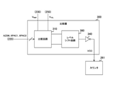
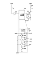
- FIG. 5 is a block diagram showing a configuration example of the column signal processing unit 260 according to the first embodiment of the present technology.
- a comparator 300, a counter 261 and a latch 262 are arranged in each column in the column signal processing unit 260.
- N is an integer
- the comparator 300, the counter 261 and the latch 262 are arranged N by N.
- the comparator 300 compares the reference signal from the DAC 230 with the pixel signal from the corresponding column.
- the potential of the reference signal is hereinafter referred to as the reference potential V RMP
- the potential of the vertical signal line 259 for transmitting the pixel signal is hereinafter referred to as the input potential V VSL .
- the comparator 300 supplies an output signal VCO indicating the comparison result to the counter 261 in the corresponding column.
- the level of the pixel signal when the pixel circuit 250 is initialized (that is, the input potential VVSL ) is hereinafter referred to as “reset level”, and is the pixel signal when the charge is transferred to the floating diffusion layer 254.
- the level is hereinafter referred to as “signal level”.
- the counter 261 counts the count value over a period until the output signal VCO is inverted.
- the counter 261 counts down, for example, over the period until the output signal VCO corresponding to the reset level is inverted, and upcounts over the period until the output signal VCO corresponding to the signal level is inverted.
- CDS Correlated Double Sampling
- the counter 261 causes the latch 262 to hold a digital signal indicating the count value.
- the comparator 300 and the counter 261 realize an AD conversion process for converting an analog pixel signal into a digital signal. That is, the comparator 300 and the counter 261 function as ADCs. ADCs that use comparators and counters in this way are commonly referred to as single-slope ADCs.
- the counter 261 may perform only one of up-counting and down-counting, and the CDS processing for obtaining the difference may be executed by the circuit in the subsequent stage.
- the latch 262 holds a digital signal.
- the latch 262 outputs the held digital signal under the control of the horizontal scanning circuit 270.
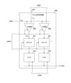
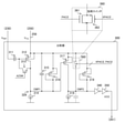
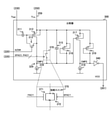
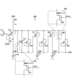
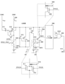
- FIG. 6 is a circuit diagram showing a configuration example of the comparator 300 according to the first embodiment of the present technology.
- the comparator 300 includes an input capacitance 311, an input transistor 312, an auto-zero transistor 313, a cutoff switch 330, a current source 314, a band limiting capacitance 315, and a clamp transistor 316. Further, the comparator 300 includes an output transistor 317, a current source 318 and a clamp transistor 319, and inverters 340 and 350.
- the input capacitance 311 is inserted between the DAC 230 and the gate of the input transistor 312.
- the source of the input transistor 312 is connected to the vertical signal line 259, and the input potential VVSL , which is the potential of the vertical signal line 259, is input to the source. Further, the reference potential VRMP is input to the gate of the input transistor 312 via the input capacitance 311. When the input potential V VSL input to the source and the reference potential V RMP input to the gate substantially match, the input transistor 312 draws a drain voltage corresponding to the input potential V VSL and the reference potential V RMP from the drain. Output.
- substantially matching means that the potentials of the comparison targets are completely matched, or the difference is within a predetermined allowable value. This allowable value is set to the threshold voltage Vt of the input transistor 312.
- a pMOS p-channel Metal-Oxide-Semiconductor
- the auto-zero transistor 313 short-circuits between the gate and drain of the input transistor 312 according to the control signal AZSW from the timing control unit 220.
- the auto-zero transistor 313 for example, a pMOS transistor is used.
- This current source 314 supplies a constant current.
- the current source 314 is realized by an nMOS (n-channel MOS) transistor or the like.
- the band limiting capacitance 315 is inserted between the vertical signal line 259 (that is, the source of the input transistor) and the current source 314. By arranging the band limiting capacity 315, it is possible to limit a predetermined band such as a low frequency band below the cutoff frequency.
- the band limiting capacity 315 is an example of the capacity described in the claims.
- the cutoff switch 330 opens and closes the path between the connection node 329 of the band limiting capacity 315 and the current source 314 and the drain of the input transistor 312 according to the control signals XPAC1 and PAC1 from the timing control unit 220. When the cutoff switch 330 is closed, the drain voltage of the input transistor 312 is output as the comparison result CMP1 from the connection node 329.
- the clamp transistor 316 is inserted between the source of the input transistor 312 and the connection node 329.
- a pMOS (n-channel MOS) transistor is used as the clamp transistor 316, and its gate is short-circuited with the drain. Further, it is desirable that the back gate and the source of the clamp transistor 316 are short-circuited.
- the clamp transistor 316 can suppress a decrease in the drain voltage when the input transistor 312 is in the off state.
- a potential lower than the input potential V VSL by the amount of the drain-source voltage of the clamp transistor 316 is hereinafter referred to as “clamp potential V CLP ”.
- the source of the output transistor 317 is connected to the vertical signal line 259, and the input potential VVSL is input to the source. Further, the gate of the output transistor 317 is connected to the drain of the input transistor 312, and the comparison result CMP1 is input.
- the output transistor 317 for example, a pMOS transistor is used. Further, it is desirable that the back gate of the output transistor 317 and the source are short-circuited.
- the output transistor 317 outputs a signal indicating whether or not the difference between the input potential VVSL input to the source and the comparison result CMP1 input to the gate exceeds a predetermined threshold voltage as the comparison result CMP2 from the drain. ..
- the comparison result CMP2 is input to the inverter 340.
- the output transistor 317 is an example of the second output transistor described in the claims.
- the drain voltage of the input transistor 312 fluctuates according to the level of the pixel signal. Therefore, when the comparison result CMP1 is input to, for example, a subsequent circuit having a fixed threshold value based on the ground potential, the timing at which the drain voltage is inverted deviates from the ideal timing at which the pixel signal and the reference signal substantially match. It may end up.
- the drain-source voltage of the input transistor 312 is input as the gate-source voltage of the output transistor 317. Since the fluctuation amount of the drain voltage of the input transistor 312 is equivalent to the fluctuation amount of the voltage of the pixel signal, the comparison result CMP2 from the output transistor 317 is inverted at the ideal timing at which the pixel signal and the reference signal substantially match. ..
- this comparison result CMP2 is connected to, for example, a subsequent circuit having a fixed threshold value based on the ground potential, the comparison result CMP2 varies depending on the pixel signal level like the comparison result CMP1, but the gain is higher than that of the comparison result CMP1. Since it is high, it is difficult to see the error. In this way, by adding the output transistor 317, it is possible to suppress the error of the inversion timing.
- the current source 318 is inserted between the drain of the output transistor 317 and the reference potential VSSB to supply a constant current.
- the current source 318 is realized by an nMOS transistor or the like.
- the clamp transistor 319 is inserted between the source and drain of the output transistor 317.
- a pMOS (n-channel MOS) transistor is used as the clamp transistor 319, and its gate is short-circuited with the drain. Further, it is desirable that the back gate and the source of the clamp transistor 319 are short-circuited.
- the clamp transistor 319 can suppress a decrease in the drain voltage when the output transistor 317 is in the off state. It is assumed that the clamp potential corresponding to the clamp transistor 319 is substantially the same as the clamp potential corresponding to the clamp transistor 316.
- clamp transistor 316, the output transistor 317 and the clamp transistor 319 are arranged in the comparator 300, a configuration in which at least one of these is not provided is also possible. If the output transistor 317 is not provided, the current source 318 and the clamp transistor 319 become unnecessary.
- the reference potential V RMP is set higher than at auto-zero at the start of the AD conversion and decreases with the passage of time within the AD conversion period.
- the AD conversion period is a period for the counter 261 to perform counting.
- the input transistor 312 of the first stage is turned off, a current flows through the clamp transistor 316, and the clamp potential V CLP lower than the input potential V VSL is compared from the connection node 329 via the cutoff switch 330. It is output as CMP1.
- the output transistor 317 of the second stage is turned on, and the input potential VVSL is output as the comparison result CMP2.
- the input transistor 312 of the first stage is turned on.
- the comparison result CMP1 is inverted to the input potential VVSL .
- the output transistor 317 of the second stage transitions to the off state, and the comparison result CMP2 is inverted to the clamp potential V CLP .
- the potential of the comparison result CMP1 is a value within the range from the clamp potential V CLP to the input potential V VSL . Further, within the counting period of the counter 261 (that is, the AD conversion period), the comparison result CMP1 output from the connection node 329 transitions from the low level (clamp potential V CLP ) to the high level (input potential V VSL ). Therefore, it is necessary to initialize the potential of the connection node 329 to a low level immediately before the AD conversion period.
- the timing control unit 220 controls the cutoff switch 330 to be in the open state for a predetermined pulse period at the timing of initializing to the low level. As a result, the connection node 329 is separated from the drain of the input transistor 312. Further, outside the pulse period, the cutoff switch 330 is controlled to be closed, and the connection node 329 is connected to the drain of the input transistor 312.
- clamp potential V CLP and the input potential V VSL output from the input transistor 312 are examples of a pair of output potentials described in the claims.
- the inverter 340 inverts the comparison result CMP2 and supplies the inverted signal to the inverter 350.
- the inverter 350 inverts the inverting signal from the inverter 340 and supplies it to the counter 261 as an output signal VCO.
- Inverters 340 and 350 are examples of logic gates described in the claims.
- FIG. 7 is a circuit diagram showing a configuration example of the cutoff switch 330 and the inverters 340 and 350 according to the first embodiment of the present technology.
- a is a circuit diagram showing a configuration example of the cutoff switch 330.
- Reference numeral b in the figure is a circuit diagram showing a configuration example of the inverters 340 and 350.
- the cutoff switch 330 includes an nMOS transistor 331 and a pMOS transistor 332 connected in parallel between the drain of the input transistor 312 and the current source 314.
- the control signal XPAC1 is input to the gate of the nMOS transistor 331, and the control signal PAC1 is input to the gate of the pMOS transistor 332.
- the control signal XPAC1 is a signal whose phase is 180 degrees different from that of PAC1.
- nMOS transistor 331 is an example of the N-type transistor described in the claims
- pMOS transistor 332 is an example of the P-type transistor described in the claims.
- the inverter 340 includes a pMOS transistor 341 and an nMOS transistor 342.
- the inverter 350 includes a pMOS transistor 351 and an nMOS transistor 352.
- the pMOS transistor 341 and the nMOS transistor 342 in the inverter 340 are connected in series between the power supply potential VDDC and the reference potential VSSC.
- the comparison result CMP2 is input to the gate of these transistors.
- An inverting signal INV is output from the connection node of the pMOS transistor 341 and the nMOS transistor 342 to the inverter 350.
- the power supply potential VDDB is a power supply potential different from the power supply potential VDDA of the pixel circuit 250.
- the reference potential VSSC is a potential different from the reference potential VSSB of the comparator 300.
- the pMOS transistor 351 and the nMOS transistor 352 in the inverter 350 are connected in series between the power supply potential VDDC and the reference potential VSSC.
- An inverting signal INV is input to the gate of these transistors.
- the output signal VCO is output from the connection node of the pMOS transistor 351 and the nMOS transistor 352 to the counter 261.
- Inverters 340 and 350 can convert the power supply potential VDDB in the previous stage to a lower power supply potential VDDC.
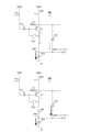
- FIG. 8 is a diagram for explaining the effect of improving responsiveness in the first embodiment of the present technology.
- a is a circuit diagram showing a configuration example of the comparator 300 of the comparative example in which the cutoff switch 330 is not provided.
- Reference numeral b in the figure is a circuit diagram showing a configuration example of the comparator 300 according to the first embodiment of the present technology.
- a comparative example of a configuration in which the drain of the input transistor 312 is connected to the connection node 329 without providing the cutoff switch 330 is assumed.
- a high level reference potential V RMP higher than the input potential V VSL is used as the input transistor. It is assumed that the input is made in 312.
- the input transistor 312 shifts to the off state, and the comparison result CMP1 transitions from the high level to the low level.
- the difference between the reference potential V RMP and the input potential V VSL is relatively small, the input transistor 312 is not completely turned off, but is weakly turned off, and a leak current flows between the drain and the source of the input transistor 312.
- the band limiting capacity 315 is discharged by the difference current between the leak current of the input transistor 312 and the constant current supplied by the current source 314.
- the thin arrow a in the figure indicates the differential current and the leak current. Thick arrows indicate constant current.
- the speed at which the comparison result CMP1 transitions to the low level according to the input is determined by the slew rate and the settling time.
- the slew rate of the first stage means the falling speed of the potential of the connection node 329 when the band limiting capacity 315 is discharged by the discharge current.
- the settling time of the first stage means the time until the potential of the connection node 329 transitions to a low level when an RC circuit including the output impedance of the input transistor 312 and the band limiting capacitance 315 is assumed.
- the larger the discharge current the higher the slew rate and the higher the response speed. Further, the larger the capacity value of the bandwidth limiting capacity 315, the longer the settling time and the lower the response speed.
- the input transistor 312 since the input transistor 312 is grounded to the source, its output impedance is relatively high at 1 / g ds , where g ds is the drain conductance. Further, in a in the figure, since the discharge is performed by the difference current (thin arrow) between the leak current and the constant current, the discharge current is smaller than that in the case where there is no leak current, and the response speed is lowered. Further, since the parasitic capacitance between the drain and the source of the input transistor 312 appears as a part of the band limiting capacitance 315, the capacitance value becomes larger than that when there is no parasitic capacitance, and the response speed decreases. The dotted line capacitance in the figure indicates the parasitic capacitance.
- the cutoff switch 330 when the cutoff switch 330 is provided and opened, the leak current is cut off, so that the discharge current becomes larger than in the comparative example. Further, since the input transistor 312 is disconnected, the capacitance value becomes smaller by the amount of the parasitic capacitance between the drain and the source. As a result, the response speed is increased as compared with the comparative example, and the responsiveness is improved.
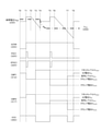
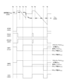
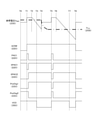
- FIG. 9 is a timing chart showing an example of the operation of the solid-state image sensor 200 according to the first embodiment of the present technology.
- the alternate long and short dash line in the figure shows the potential (input potential V VSL ) of the vertical signal line 259.
- the DAC 230 sets the reference potential V RMP to the auto-zero potential VAZ . Further, the timing control unit 220 lowers the control signal AZSW to a low level. As a result, the comparison results CMP1 and CMP2 have an auto-zero potential VAZ . Further, the control signal PAC1 is controlled at a low level, and the control signal XPAC1 is controlled at a high level. As a result, the cutoff switch 330 is closed.
- the timing control unit 220 sets the control signal AZSW to a high level. Further, in the timing T1, the timing control unit 220 sets the control signal PAC1 at a high level and the control signal XPAC1 at a low level over a predetermined pulse period. As a result, the cutoff switch 330 is opened.
- the DAC 230 raises the reference potential V RMP higher than at auto zero.
- the input transistor 312 is turned off, and the comparison result CMP1 of the clamp potential V CLP is output.
- the clamp potential at this time is higher than the clamp potential corresponding to the signal level, and this potential is defined as VCLPH .
- the output transistor 317 is turned on and outputs the CMP2, which is the comparison result of the reset level VVSLL .
- the inverter 350 outputs a high-level output signal VCO.
- the comparison results CMP1, CMP2, and the output signal VCO do not actually make an instantaneous transition from one of the high level and the low level to the other, and it takes a predetermined time according to a time constant or the like until the transition is completed. ..
- the waveform is described as an instantaneous transition.
- the DAC 230 lowers the reference potential VRMP with the passage of time. This period corresponds to the reset level AD conversion period. It is assumed that the difference between the reference potential V RMP and the input potential V VSL becomes less than the threshold voltage Vt of the input transistor 312 at the timing T3 within this period. At this time, the input transistor 312 transitions to the ON state, and the comparison result CMP1 is inverted to the reset level VVSLL . The output transistor 317 transitions to the off state, and the comparison result CMP2 is inverted to the clamp potential VCLPH . The output signal VCO is inverted to the low level.
- the timing control unit 220 sets the control signal PAC1 to a high level and the control signal XPAC1 to a low level over a predetermined pulse period. As a result, the cutoff switch 330 is opened.
- the DAC 230 raises the reference potential VRMP to be higher than that at the time of auto zero.
- the input transistor 312 is turned off, and the comparison result CMP1 of the clamp potential V CLP is output.
- the clamp potential at this time is lower than the clamp potential corresponding to the black level, and this potential is defined as V CLPL .
- the output transistor 317 is turned on and outputs the comparison result CMP2 of the signal level VVSLL .
- the inverter 350 outputs a high-level output signal VCO.
- the DAC 230 lowers the reference potential VRMP over time. This period corresponds to the signal level AD conversion period. It is assumed that the difference between the reference potential V RMP and the input potential V VSL becomes less than the threshold voltage Vt at the timing T7 within this period. At this time, the comparison result CMP1 is inverted to the signal level VVSLL , and the comparison result CMP2 is inverted to the clamp potential VCLPL . The output signal VCO is inverted to the low level.
- the timing control unit 220 controls the cutoff switch 330 in the open state over a predetermined pulse period at the timings T1 and T5 immediately before the AD conversion period.
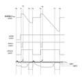
- FIG. 10 is an example of a timing chart when a black level is input within the signal level conversion period in the first embodiment of the present technology.
- a is a diagram showing an example of the waveform of the potential of the vertical signal line 259 (input potential V VSL ) and the reference potential V RMP .
- b is a diagram showing an example of the waveform of the comparison result CMP1 in the comparative example without the cutoff switch 330.
- c is a diagram showing an example of the waveform of the comparison result CMP1 in the first embodiment provided with the cutoff switch 330.
- a black level that is substantially the same as the reset level is input as the signal level.
- the slope when the comparison result CMP1 transitions from the high level to the low level is gentle, and the time until the transition to the low level becomes long.
- the thick line in the figure shows the trajectory of the transition from high level to low level. Further, immediately after the timings T2 and T6, since the transition to the high level is started before the clamp potential is lowered, the transition from the low level to the high level is started at the time of reset level conversion and at the time of signal level conversion. The amplitude is different. In the figure, the line segments with arrows at both ends indicate the magnitude of the amplitude. This may deteriorate the characteristics of the comparator 300.
- the slope at the time of transition from high level to low level becomes steep due to the cutoff of leakage current and parasitic capacitance, and the slope becomes low level.
- the time to transition is shortened.
- the transition to the high level is started after the voltage drops to the clamp potential, the amplitude from the low level to the high level becomes the same at the time of reset level conversion and at the time of signal level conversion. As a result, deterioration of the characteristics of the comparator 300 can be suppressed.
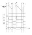
- FIG. 11 is an example of a timing chart when a white level is input within the signal level conversion period in the first embodiment of the present technology.
- a is a diagram showing an example of the waveform of the potential of the vertical signal line 259 (input potential V VSL ) and the reference potential V RMP .
- b is a diagram showing an example of the waveform of the comparison result CMP1 in the comparative example without the cutoff switch 330.
- c is a diagram showing an example of the waveform of the comparison result CMP1 in the first embodiment provided with the cutoff switch 330.
- a white level lower than the reset level is input as the signal level.
- the time until the comparison result CMP1 transitions to the low level becomes long. Further, the amplitude from the low level to the high level differs between the time of reset level conversion and the time of signal level conversion.
- the cutoff switch 330 when the cutoff switch 330 is provided as illustrated in c in the figure, the time until the transition to the low level is shortened due to the cutoff of the leak current and the parasitic capacitance. Further, the amplitude from the low level to the high level becomes the same when the reset level is converted and when the signal level is converted.
- FIG. 12 is a flowchart showing an example of the operation of the solid-state image sensor 200 according to the first embodiment of the present technology. This operation is started, for example, when a predetermined application for capturing image data is executed.
- the vertical scanning circuit 210 selects a read line and exposes it (step S911).
- the cutoff switch 330 disconnects the input transistor 312 from the connection node 329 within the pulse period (step S912).
- the column signal processing unit 260 AD-converts the reset level for each column (step S913).
- the cutoff switch 330 disconnects the input transistor 312 from the connection node 329 within the pulse period (step S914).
- the column signal processing unit 260 AD-converts the signal level for each column (step S915). Then, the vertical scanning circuit 210 determines whether or not the read line is the last line (step S916).
- step S916: No If the read row is not the last row (step S916: No), the solid-state image sensor 200 repeats steps S911 and subsequent steps. On the other hand, when the read row is the final row (step S916: Yes), the solid-state image sensor 200 ends the operation for imaging.
- timing chart illustrated in FIG. 9 corresponds to steps S912 to S915 in FIG.
- steps S911 to S916 are repeatedly executed in synchronization with the vertical synchronization signal.
- the cutoff switch 330 disconnects the input transistor 312 from the connection node 329, the leakage current of the input transistor 312 is cut off and the parasitic capacitance is disconnected from the connection node 329. Can be done. Thereby, the responsiveness of the comparator 300 can be improved.
- the cutoff switch 330 including the nMOS transistor 331 and the pMOS transistor 332 is arranged for each column.
- the number of transistors is larger than in the case where the cutoff switch 330 is realized by one transistor.
- the solid-state image sensor 200 of the first modification of the first embodiment is different from the first embodiment in that a cutoff switch 330 including only the nMOS transistor 331 is used.
- FIG. 13 is a circuit diagram showing a configuration example of the comparator 300 in the first modification of the first embodiment of the present technology.
- the comparator 300 of the first modification of the first embodiment is different from the first embodiment in that the cutoff switch 330 including only the nMOS transistor 331 is arranged.
- the waveform of the control signal XPAC1 that controls the nMOS transistor 331 is the same as that of the first embodiment.
- the number of transistors can be reduced as compared with the case where a pair of transistors (nMOS transistor 331 and pMOS transistor 332) are used.
- the cutoff switch 330 composed of only the nMOS transistor 331 is used, the number of transistors is increased as compared with the case where a pair of transistors are used. Can be reduced.
- the cutoff switch 330 including the nMOS transistor 331 and the pMOS transistor 332 is arranged for each column.
- the number of transistors is larger than in the case where the cutoff switch 330 is realized by one transistor.
- the solid-state image sensor 200 of the second modification of the first embodiment is different from the first embodiment in that a cutoff switch 330 including only the pMOS transistor 332 is used.
- FIG. 14 is a circuit diagram showing a configuration example of the comparator 300 in the second modification of the first embodiment of the present technology.
- the comparator 300 of the second modification of the first embodiment is different from the first embodiment in that the cutoff switch 330 including only the pMOS transistor 332 is arranged.
- the waveform of the control signal PAC1 that controls the pMOS transistor 332 is the same as that of the first embodiment.
- the number of transistors can be reduced as compared with the case where a pair of transistors (nMOS transistor 331 and pMOS transistor 332) are used.
- the cutoff switch 330 can be realized by using only the nMOS transistor 331 or only the pMOS transistor 332.
- the nMOS transistor 331 is used.
- the pMOS transistor 332 is used.
- both the nMOS transistor 331 and the pMOS transistor 332 are used as in the first embodiment.
- the cutoff switch 330 composed of only the pMOS transistor 332 is used, the number of transistors is increased as compared with the case where a pair of transistors are used. Can be reduced.
- Second Embodiment> In the first embodiment described above, the time required for the comparison result CMP1 to transition to the low level is shortened by the cutoff switch 330. However, with the cutoff switch 330, it may not be possible to sufficiently increase the response speed until the CMP2 of the second stage comparison result reaches a high level.
- the solid-state image sensor 200 of the second embodiment is different from the first embodiment in that the responsiveness is improved by short-circuiting the source and drain of the output transistor 317.
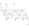
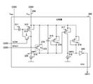
- FIG. 15 is a circuit diagram showing a configuration example of the comparator 300 according to the second embodiment of the present technology.
- the comparator 300 of the second embodiment is different from the first embodiment in that the output side short circuit switch 360 is provided instead of the cutoff switch 330. Further, the drain of the input transistor 312 of the second embodiment is connected to the connection node 329.
- the output-side short-circuit switch 360 opens and closes a path between the source of the output transistor 317 (in other words, the vertical signal line 259) and its drain according to the control signals XPAC2 and PAC2 from the timing control unit 220.
- the output-side short-circuit switch 360 includes, for example, an nMOS transistor 361 and a pMOS transistor 362 connected in parallel between the source and drain of the output transistor 317.
- the control signal PAC2 is input to the gate of the nMOS transistor 361, and the control signal XPAC2 is input to the gate of the pMOS transistor 362.
- the control signal XPAC2 is a signal whose phase is 180 degrees different from that of PAC2.
- nMOS transistor 361 is an example of the N-type transistor described in the claims
- pMOS transistor 362 is an example of the P-type transistor described in the claims.
- the potential of the second-stage comparison result CMP2 is a value within the range from the clamp potential V CLP to the input potential V VSL . Further, within the counting period (AD conversion period) of the counter 261 the comparison result CMP2 from the drain of the output transistor 317 transitions from the high level (input potential V VSL ) to the low level (clamp potential V CLP ). Therefore, it is necessary to initialize the drain of the output transistor 317 to a high level immediately before the AD conversion period.
- the speed at which the comparison result CMP2 transitions to a high level according to the input is determined by the slew rate and the settling time.
- the slew rate of the second stage means the rising speed of the drain when the parasitic capacitance on the drain side of the output transistor 317 is charged by the charging current from the output transistor 317.
- the second-stage settling time means the time until the drain potential transitions to a high level when an RC circuit including the output impedance of the output transistor 317 and the parasitic capacitance is assumed.
- the dotted line capacitance in the figure indicates the parasitic capacitance.
- comparison result CMP2 of the second stage is linked to the comparison result CMP1 of the first stage, and when the response speed of the first stage decreases, the response speed of the second stage also decreases.
- the timing control unit 220 controls the output side short-circuit switch 360 to be closed for a predetermined pulse period at the timing of initializing to a high level.
- the source (vertical signal line 259) of the output transistor 317 and the drain are short-circuited. Since the potential of the vertical signal line 259 is at a high level (input potential VVSL ), the speed at which the comparison result CMP2 transitions to the high level can be increased by a short circuit. Further, even in the auto-zero period, the output side short-circuit switch 360 is controlled to be in the closed state.
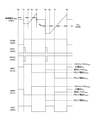
- FIG. 16 is a timing chart showing an example of the operation of the solid-state image sensor 200 according to the second embodiment of the present technology.
- timing control unit 220 sets the control signal PAC2 to a high level and the control signal XPAC2 to a low level. As a result, the cutoff switch 330 is closed.
- the timing control unit 220 keeps the control signal PAC2 at the high level and the control signal XPAC2 at the low level.
- the control signal PAC2 is controlled to a low level and the control signal XPAC2 is controlled to a high level.
- the cutoff switch 330 is opened.
- the timing control unit 220 sets the control signal PAC2 to a high level and the control signal XPAC1 to a low level over a predetermined pulse period. As a result, the output side short-circuit switch 360 is closed. After the pulse period elapses, the control signal PAC2 is controlled to a low level and the control signal XPAC2 is controlled to a high level. As a result, the cutoff switch 330 is opened.
- the timing control unit 220 controls the output side short-circuit switch 360 in the closed state for a predetermined pulse period at the timings T1 and T5 immediately before the AD conversion period.
- the speed (response speed) at which the comparison result CMP2 transitions to a high level can be increased.
- the timing control unit 220 controls the output side short-circuit switch 360 to the closed state even within the auto-zero period from the timing T0 to the timing T1.
- a loop circuit is formed by the input transistor 312 of the first stage, the output transistor 317 of the second stage, and the vertical signal line 259, and the loop circuit may oscillate within the auto-zero period.
- the output side short-circuit switch 360 by controlling the output side short-circuit switch 360 to be in the closed state even during the auto-zero period, oscillation within the auto-zero period can be suppressed.
- FIG. 17 is an example of a timing chart when a black level is input within the signal level conversion period in the second embodiment of the present technology.
- a is a diagram showing an example of the waveform of the potential of the vertical signal line 259 (input potential V VSL ) and the reference potential V RMP .
- b is a diagram showing an example of the waveform of the comparison result CMP2 in the comparative example without the output side short-circuit switch 360.
- c is a diagram showing an example of the waveform of the comparison result CMP2 in the second embodiment provided with the output side short-circuit switch 360.
- a black level that is substantially the same as the reset level is input as the signal level.
- the slope when the comparison result CMP2 transitions from the low level to the high level is gentle, and the time until the transition to the high level becomes long. ..
- the thick line in the figure shows the trajectory of the transition from low level to high level.
- the amplitude from the high level to the low level increases between the time of reset level conversion and the time of signal level conversion. different. This may deteriorate the characteristics of the comparator 300.
- FIG. 18 is an example of a timing chart when a white level is input within the signal level conversion period in the second embodiment of the present technology.
- a is a diagram showing an example of the waveform of the potential of the vertical signal line 259 (input potential V VSL ) and the reference potential V RMP .
- b is a diagram showing an example of the waveform of the comparison result CMP2 in the comparative example without the output side short-circuit switch 360.
- c is a diagram showing an example of the waveform of the comparison result CMP2 in the second embodiment provided with the output side short-circuit switch 360.
- a white level lower than the reset level is input as the signal level.
- the time until the comparison result CMP2 transitions to the high level becomes long. Further, the amplitude from the high level to the low level differs between the time of reset level conversion and the time of signal level conversion.
- the output side short circuit switch 360 is provided as illustrated in c in the figure, the time until the transition to the high level is shortened due to the short circuit. Further, the amplitude from the high level to the low level becomes the same at the time of conversion of the reset level and at the time of conversion of the signal level.
- the comparison result CMP2 is set to the potential (high level) of the source.
- the transition speed can be increased. Thereby, the responsiveness can be improved.
- the output side short-circuit switch 360 including the nMOS transistor 361 and the pMOS transistor 362 is arranged for each column.
- the number of transistors is larger than in the case where the output side short-circuit switch 360 is realized by one transistor.
- the solid-state image sensor 200 of the first modification of the second embodiment is different from the first embodiment in that the output side short-circuit switch 360 including only the nMOS transistor 361 is used.
- FIG. 19 is a circuit diagram showing a configuration example of the comparator 300 in the first modification of the second embodiment of the present technology.
- the comparator 300 of the first modification of the second embodiment is different from the second embodiment in that the output side short circuit switch 360 including only the nMOS transistor 361 is arranged.
- the waveform of the control signal PAC2 that controls the nMOS transistor 361 is the same as that of the second embodiment.
- the number of transistors can be reduced as compared with the case where a pair of transistors (nMOS transistor 361 and pMOS transistor 362) are used.
- the output side short-circuit switch 360 composed of only the nMOS transistor 361 is used, the transistor is compared with the case where a pair of transistors is used. The number can be reduced.
- the output side short-circuit switch 360 including the nMOS transistor 361 and the pMOS transistor 362 is arranged for each column.
- the number of transistors is larger than in the case where the output side short-circuit switch 360 is realized by one transistor.
- the solid-state image sensor 200 of the second modification of the second embodiment is different from the first embodiment in that the output side short-circuit switch 360 including only the pMOS transistor 362 is used.
- FIG. 20 is a circuit diagram showing a configuration example of the comparator 300 in the second modification of the second embodiment of the present technology.
- the comparator 300 of the second modification of the second embodiment is different from the second embodiment in that the output side short circuit switch 360 including only the pMOS transistor 362 is arranged.
- the waveform of the control signal XPAC2 that controls the pMOS transistor 362 is the same as that of the second embodiment.
- the number of transistors can be reduced as compared with the case where a pair of transistors (nMOS transistor 361 and pMOS transistor 362) are used.
- the output side short-circuit switch 360 can be realized by using only the nMOS transistor 361 or only the pMOS transistor 362.
- Second stage comparison result When the level of CMP2 is relatively low, the nMOS transistor 361 is used. On the other hand, when the level of the CMP2 in the second stage is relatively high, the pMOS transistor 362 is used. Further, when the level of the comparison result CMP2 is about the middle of the power supply potential VDDB, both the nMOS transistor 361 and the pMOS transistor 362 are used as in the second embodiment.
- the transistor is compared with the case where a pair of transistors is used. The number can be reduced.
- the time required for the comparison result CMP1 to transition to the low level is shortened by the cutoff switch 330.
- the cutoff switch 330 alone may not be able to sufficiently increase the response speed until the CMP2 in the second stage comparison result reaches a high level.
- the solid-state image sensor 200 of the third embodiment is different from the first embodiment in that the responsiveness is further improved by adding a switch that short-circuits the source and drain of the output transistor 317.
- FIG. 21 is a circuit diagram showing a configuration example of the comparator 300 according to the third embodiment of the present technology.
- the comparator 300 of the third embodiment is different from the first embodiment in that it further includes an output side short circuit switch 360.
- This output-side short-circuit switch 360 is realized only by the pMOS transistor 362, as in the second modification of the second embodiment.
- the third embodiment is an application of the second modification of the second embodiment to the first embodiment.
- the speed at which the output of the second stage transitions to the high level can be increased, and the responsiveness of the comparator 300 can be further improved.
- nMOS transistor 331 and the pMOS transistor 332 are provided in the cutoff switch 330, only one of these may be provided.
- the output side short-circuit switch 360 is realized only by the pMOS transistor 362, but the configuration is not limited to this. Both the nMOS transistor 361 and the pMOS transistor 362 may be provided in the output side short-circuit switch 360, or only the nMOS transistor 361 may be provided.
- FIG. 22 is a timing chart showing an example of the operation of the solid-state image sensor 200 according to the third embodiment of the present technology.
- the timing control unit 220 further supplies the control signal XPAC2 to control the output side short-circuit switch 360.
- the waveform of the control signal XPAC2 is the same as that of the second modification of the second embodiment.
- the comparison result CMP2 is set to the potential (high level) of the source.
- the transition speed can be increased. Thereby, the responsiveness can be further improved.
- FIG. 23 is a circuit diagram showing a configuration example of the comparator 300 according to the fourth embodiment of the present technology.
- the comparator 300 of the fourth embodiment is different from the third embodiment in that the inverter 340 is not arranged and the output transistor 320, the current source 321 and the clamp transistor 322 are provided.
- the source of the output transistor 320 is connected to the vertical signal line 259, and the input potential VVSL is input to the source. Further, the gate of the output transistor 320 is connected to the drain of the second stage output transistor 317, and the comparison result CMP2 is input.
- the output transistor 320 of the third stage for example, a pMOS transistor is used. Further, it is desirable that the back gate of the output transistor 320 and the source are short-circuited.
- the output transistor 320 outputs a signal indicating whether or not the difference between the input potential VVSL input to the source and the comparison result CMP2 input to the gate exceeds a predetermined threshold voltage as the comparison result CMP3 from the drain. ..
- the comparison result CMP3 is input to the inverter 350.
- the output transistor 320 is an example of the second output transistor described in the claims.
- the current source 321 is inserted between the drain of the output transistor 320 and the reference potential VSSB to supply a constant current.
- the current source 321 is realized by an nMOS transistor or the like.
- the clamp transistor 322 is inserted between the source and drain of the output transistor 320.
- a pMOS transistor is used as the clamp transistor 322, the gate of which is shorted to the drain. Further, it is desirable that the back gate and the source of the clamp transistor 322 are short-circuited.
- the inverter 340 is reduced because the output transistor 320 is added to the third stage.
- both the cutoff switch 330 and the output side short-circuit switch 360 are arranged, only one of them can be arranged. Further, both the cutoff switch 330 and the output side short-circuit switch 360 may be provided with both an nMOS transistor and a pMOS transistor, or only one of them may be provided.
- the output transistor 320 for determining whether or not the difference between the input potential VVSL and the comparison result CMP2 exceeds a predetermined threshold voltage is added to the third stage. Therefore, the gain of the comparator 300 is increased and the linearity is improved.
- the cutoff switch 330 disconnects the drain of the input transistor 312 from the connection node 329 immediately before the AD conversion, and the input transistor 312 has transitioned to the off state.
- the drain of the input transistor 312 in the off state becomes a high impedance node. Since the potential of the high impedance node fluctuates easily due to capacitive coupling, the potential of the gate of the input transistor 312 fluctuates due to the fluctuation, and the characteristics of the comparator 300 may deteriorate.
- the solid-state image sensor 200 of the fifth embodiment is different from the third embodiment in that the deterioration of the characteristics is suppressed by the short circuit between the source and the drain of the input transistor 312.
- FIG. 24 is a circuit diagram showing a configuration example of the comparator 300 according to the fifth embodiment of the present technology.
- the comparator 300 of the fifth embodiment further includes an input side short circuit switch 370.
- the input side short-circuit switch 370 opens and closes the path between the source (vertical signal line 259) and the drain of the input transistor 312 according to the control signals PAC1 and XPAC1.
- the input side short-circuit switch 370 includes, for example, an nMOS transistor 371 and a pMOS transistor 372 connected in parallel between the source and the drain of the input transistor 312.
- the control signal PAC1 is input to the gate of the nMOS transistor 371, and the control signal XPAC1 is input to the gate of the pMOS transistor 372.
- the input side short-circuit switch 370 is closed when the cutoff switch 330 is opened, short-circuiting the source and drain of the input transistor 312. As a result, it is possible to prevent the drain of the input transistor 312 from becoming a high impedance node and suppress deterioration of characteristics.
- both the cutoff switch 330 and the output side short-circuit switch 360 are arranged, only one of them can be arranged. Further, both the nMOS transistor and the pMOS transistor may be provided in each of the cutoff switch 330, the output side short circuit switch 360, and the input side short circuit switch 370, or only one of them may be provided. Further, the fourth embodiment can be applied to the fifth embodiment.
- the input side short-circuit switch 370 short-circuits the source and drain of the input transistor 312, it is possible to prevent the drain from being in a high impedance state. .. As a result, deterioration of the characteristics of the comparator 300 can be suppressed.
- the output transistor 317 inputs the comparison result CMP2 to the inverter 340, but if the voltage range thereof is narrow, the inverter 340 may malfunction or a leak current may occur.
- the solid-state image sensor 200 of the sixth embodiment is different from the third embodiment in that a level shift circuit for expanding the voltage range is added.
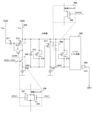
- FIG. 25 is a circuit diagram showing a configuration example of the comparator 300 according to the sixth embodiment of the present technology.
- the comparator 300 of the sixth embodiment is different from the third embodiment in that it does not include the inverter 340 and further includes the level shift circuit 380.
- the level shift circuit 380 outputs one of a pair of potentials (in other words, high level and low level) having a potential difference larger than that of the input potential V VSL and the clamp potential V CLP as an output signal to the inverter 350 based on the comparison result CMP2. do.
- the high level is set, for example, to a power supply potential higher than the input potential VVSL .
- the low level is set, for example, to a reference potential lower than the clamp potential V CLP .
- the input potential V VSL and the clamp potential V CLP are examples of the pair of output potentials described in the claims.
- the power supply potential and the reference potential are examples of the pair of shift potentials described in the claims.
- the level shift circuit 380 By providing the level shift circuit 380, the voltage range on the input side of the inverter 350 can be expanded as compared with the third embodiment. By expanding the voltage range, the difference between the lower limit and the upper limit of the range and the threshold value of the inverter 350 becomes sufficiently large, and it is possible to prevent malfunction and leakage current of the inverter 350. As a result, design restrictions for preventing malfunction and leakage current of the inverter 350 are alleviated, and the degree of freedom in design is improved.
- the level shift circuit 380 expands both the power supply side and the ground side, but only one of them may be expanded.
- both the cutoff switch 330 and the output side short-circuit switch 360 are arranged, only one of them can be arranged. Further, both the nMOS transistor and the pMOS transistor may be provided in each of the cutoff switch 330, the output side short circuit switch 360, and the input side short circuit switch 370, or only one of them may be provided. Further, the fourth embodiment and the fifth embodiment can be applied to the sixth embodiment.
- FIG. 26 is a circuit diagram showing a configuration example of the level shift circuit 380 according to the sixth embodiment of the present technology.
- the level shift circuit 380 includes a precharge transistor 381 and an nMOS transistor 382, a pMOS transistor 384 and a precharge transistor 385.
- a precharge transistor 381 for example, a pMOS transistor is used.
- a precharge transistor 385 for example, an nMOS transistor is used.
- the source of the precharge transistor 381 is connected to the power supply potential VDDB, and the control signal PreChg1 from the timing control unit 220 is input to the gate.
- the drain of the precharge transistor 381 is connected to the drain of the nMOS transistor 382.
- the power supply potential VDDB is a potential different from the power supply potential VDDA of the pixel circuit 250 and the power supply potential VDDC of the inverter.
- the gate of the nMOS transistor 382 is connected to the vertical signal line 259, and the comparison result CMP2 from the output transistor 317 is input to the source. Further, the connection node of the precharge transistor 381 and the nMOS transistor 382 is connected to the gate of the pMOS transistor 384, and the output signal nOUT is output from the connection node. The back gate and source of the nMOS transistor 382 are short-circuited.
- the source of the pMOS transistor 384 is connected to the power supply potential VDDB, and the gate is connected to the connection node of the precharge transistor 381 and the nMOS transistor 382.
- the output signal pOUT is output from the connection node of the pMOS transistor 384 and the precharge transistor 381.
- the drain of the pMOS transistor 384 is connected to the drain of the precharge transistor 385.
- the source of the precharge transistor 385 is connected to the reference potential VSSB, and the control signal PreChg2 is input to the gate. Further, the connection node of the pMOS transistor 384 and the precharge transistor 385 is connected to the inverter 350, and the output signal pOUT is output from the connection node.
- the precharge transistor 381 is an example of the power supply side precharge transistor described in the claims.
- the nMOS transistor 382 is an example of the N-type transistor described in the claims.
- the pMOS transistor 384 is an example of the P-type transistor described in the claims.
- the precharge transistor 385 is an example of the reference side precharge transistor described in the claims.
- the timing control unit 220 turns on the precharge transistors 381 and 385 by the control signals PreChg1 and PreChg2.
- the precharge transistor 381 in the ON state precharges the parasitic capacitance 383 and initializes the drain of the nMOS transistor 382 to the power supply potential VDDB.
- the precharge transistor 385 in the ON state precharges the parasitic capacitance 386 and initializes the drain of the nMOS transistor 382 to the reference potential VSSB. Further, during the AD conversion period, the precharge transistors 381 and 385 are controlled to the off state.
- the comparison result CMP2 becomes the input potential VVSL (high level).
- the nMOS transistor 382 is turned off, and the precharged power supply potential VDDB of the parasitic capacitance 383 is output as an output signal nOUT.
- the pMOS transistor 384 is turned off, and the precharged reference potential VSSB of the parasitic capacitance 386 is output as the output signal pOUT.
- the nMOS transistor 382 transitions to the ON state, and the potential of the output signal nOUT is inverted to the clamp potential V CLP .
- the pMOS transistor 384 transitions to the ON state, and the potential of the output signal pOUT is inverted to the power supply potential VDDB.
- the configuration may be such that the pMOS transistor 384 and the precharge transistor 385 are not provided.
- the inverter 340 is added, and the output signal nOUT is output to the inverter 340. Further, the back gate of the nMOS transistor 382 can be grounded.
- FIG. 27 is a timing chart showing an example of the operation of the solid-state image sensor 200 according to the sixth embodiment of the present technology.
- the timing control unit 220 sets the control signal PreChg1 to a low level and the control signal PreChg2 to a high level between the timing T0 and immediately after the timing T1 (when the pulse period has elapsed from the timing T1). As a result, the precharge transistors 381 and 385 are precharged. Until the subsequent timing T5, the control signal PreChg1 is controlled to a high level, and the control signal PreChg2 is controlled to a low level.
- the timing control unit 220 sets the control signal PreChg1 to a low level and the control signal PreChg2 to a high level from the timing T5 over a pulse period to precharge the precharge transistors 381 and 385.
- the control signal PreChg1 is controlled to a high level
- the control signal PreChg2 is controlled to a low level.
- the output of the second stage becomes the auto-zero potential VAZ . Therefore, when the output side short-circuit switch 360 is opened during that period, the nMOS transistor 382 There is a potential difference between the gate and the source. Due to this potential difference, the nMOS transistor 382 is turned on, and a leak current may flow from the power supply potential VDDB to the precharge transistor 381, the nMOS transistor 382, and the current source 318. However, as illustrated in the figure, during the auto-zero period, the output side short-circuit switch 360 is controlled to the closed state by the control signal XPAC2, so that the nMOS transistor 382 is turned off. By closing the output-side short-circuit switch 360 within the auto-zero period in this way, it is possible to prevent leakage current in addition to suppressing oscillation.
- the inverter 350 since the level shift circuit 380 outputs one of a pair of potentials having a potential difference larger than that of the input potential V VSL and the clamp potential V CLP , the inverter 350 The voltage range on the input side of the can be expanded. By expanding the voltage range, the difference between the lower limit and the upper limit of the range and the threshold value of the inverter 350 becomes sufficiently large, and it is possible to prevent malfunction and leakage current of the inverter 350. As a result, design restrictions on the power supply voltage and the threshold value for preventing malfunction and leakage current are alleviated, and the degree of freedom in design can be improved.
- the lamp signal whose level (reference potential VRMP ) gradually decreases within the AD conversion period is used, but a lamp signal whose level gradually increases can also be used.
- the solid-state image sensor 200 of the seventh embodiment is different from the first embodiment in that a lamp signal whose level gradually rises is used.
- FIG. 28 is a circuit diagram showing a configuration example of the comparator 300 according to the seventh embodiment of the present technology.
- the comparator 300 of the seventh embodiment is different from the first embodiment in that it does not include the cutoff switch 330 and the inverter 350, and further includes the input side short circuit switch 370.
- the input side short circuit switch 370 opens and closes the path between the source (vertical signal line 259) and the drain of the input transistor 312 according to the control signals PAC1 and XPAC1.
- the input side short-circuit switch 370 includes, for example, an nMOS transistor 371 and a pMOS transistor 372 connected in parallel between the source and the drain of the input transistor 312.
- the control signal PAC1 is input to the gate of the nMOS transistor 371, and the control signal XPAC1 is input to the gate of the pMOS transistor 372.
- FIG. 29 is a timing chart showing an example of the operation of the solid-state image sensor 200 according to the seventh embodiment of the present technology.
- the DAC 230 sets the reference potential V RMP to the auto-zero potential VAZ . Further, the timing control unit 220 lowers the control signal AZSW to a low level. As a result, the comparison results CMP1 and CMP2 have an auto-zero potential VAZ . Further, the control signal PAC1 is controlled at a low level, and the control signal XPAC1 is controlled at a high level. As a result, the input side short-circuit switch 370 is opened.
- the timing control unit 220 sets the control signal AZSW to a high level. Further, in the timing T1, the timing control unit 220 sets the control signal PAC1 at a high level and the control signal XPAC1 at a low level over a predetermined pulse period. As a result, the input side short-circuit switch 370 is closed.
- the DAC 230 lowers the reference potential VRMP below that at autozero. As a result, the input transistor 312 is turned on, and the comparison result CMP1 of the reset level VVSLH is output. During this period, the output transistor 317 is turned off, and the comparison result CMP2 of the clamp potential VCLPH is output. Further, the inverter 350 outputs a high-level output signal VCO.
- the DAC 230 raises the reference potential VRMP with the passage of time. This period corresponds to the reset level AD conversion period. It is assumed that the difference between the reference potential V RMP and the input potential V VSL becomes less than the threshold voltage Vt of the input transistor 312 at the timing T3 within this period. At this time, the input transistor 312 transitions to the off state, and the comparison result CMP1 is inverted to the clamp potential VCLPH . The output transistor 317 transitions to the on state, and the comparison result CMP2 is inverted to the reset level VVSLH . The output signal VCO is inverted to the low level.
- the timing control unit 220 sets the control signal PAC1 to a high level and the control signal XPAC1 to a low level over a predetermined pulse period. As a result, the input side short-circuit switch 370 is closed.
- the DAC 230 lowers the reference potential VRMP to be lower than that at the time of auto zero.
- the input transistor 312 is turned on, and the comparison result CMP1 of the signal level VVSLL is output.
- the output transistor 317 is turned off, and the comparison result CMP2 of the clamp potential V CLPL is output.
- the inverter 350 outputs a high-level output signal VCO.
- the DAC 230 raises the reference potential VRMP with the passage of time. This period corresponds to the signal level AD conversion period. It is assumed that the difference between the reference potential V RMP and the input potential V VSL becomes less than the threshold voltage Vt at the timing T7 within this period. At this time, the comparison result CMP1 is inverted to the clamp potential V CLPL , and the comparison result CMP2 is inverted to the signal level V VSLL . The output signal VCO is inverted to the low level.
- the responsiveness can be improved by the input side short-circuit switch 370.
- the input side short-circuit switch 370 including the nMOS transistor 371 and the pMOS transistor 372 is arranged for each column.
- the number of transistors is larger than in the case where the input side short-circuit switch 370 is realized by one transistor.
- the solid-state image sensor 200 of the first modification of the seventh embodiment is different from the seventh embodiment in that the input side short-circuit switch 370 including only the nMOS transistor 371 is used.
- FIG. 30 is a circuit diagram showing a configuration example of the comparator 300 in the first modification of the seventh embodiment of the present technology.
- the comparator 300 of the first modification of the seventh embodiment is different from the first embodiment in that the input side short circuit switch 370 composed of only the nMOS transistor 371 is arranged.
- the waveform of the control signal PAC1 that controls the nMOS transistor 371 is the same as that of the seventh embodiment.
- the transistor is compared with the case where a pair of transistors is used. The number can be reduced.
- the input side short-circuit switch 370 including the nMOS transistor 371 and the pMOS transistor 372 is arranged for each column.
- the number of transistors is larger than in the case where the input side short-circuit switch 370 is realized by one transistor.
- the solid-state image sensor 200 of the second modification of the seventh embodiment is different from the first embodiment in that the input side short-circuit switch 370 including only the pMOS transistor 372 is used.
- FIG. 31 is a circuit diagram showing a configuration example of the comparator 300 in the second modification of the seventh embodiment of the present technology.
- the comparator 300 of the second modification of the seventh embodiment is different from the seventh embodiment in that the input side short circuit switch 370 composed of only the pMOS transistor 372 is arranged.
- the waveform of the control signal XPAC1 that controls the pMOS transistor 372 is the same as that of the seventh embodiment.
- the transistor is compared with the case where a pair of transistors is used. The number can be reduced.
- the two-stage transistor of the input transistor 312 and the output transistor 317 is arranged, but a third-stage transistor having the same configuration as the output transistor 317 can be added.
- the solid-state image sensor 200 of the third modification of the seventh embodiment is different from the seventh embodiment in that a third-stage transistor is added.
- FIG. 32 is a block diagram showing a configuration example of the comparator 300 in the third modification of the seventh embodiment of the present technology.
- the comparator 300 of the third modification of the seventh embodiment includes a comparator circuit 310 and inverters 340 and 350.
- FIG. 33 is a circuit diagram showing a configuration example of the comparison circuit 310 in the third modification of the seventh embodiment of the present technology.
- the comparison circuit 310 includes an input capacitance 311, an input transistor 312, an auto-zero transistor 313, an input side short-circuit switch 370, a current source 314, a band limiting capacitance 315, and a clamp transistor 316 in the first stage. Further, the comparison circuit 310 includes an output transistor 317, a current source 318, and a clamp transistor 319 in the second stage.
- the comparison circuit 310 includes an output transistor 320, a current source 321 and a clamp transistor 322 and an output side short-circuit switch 360 in the third stage.
- the circuit configurations of the first stage and the second stage in FIG. 33 are the same as those illustrated in FIG. 31. Further, the circuit configuration of the third stage in FIG. 33 is the same as that in which the output side short-circuit switch 360 is added to the third stage of FIG. 23.
- the output-side short-circuit switch 360 opens and closes the path between the source (vertical signal line 259) and the drain of the output transistor 320 according to the control signal XPAC3.
- the waveform of the control signal XPAC3 is the same as that of the control signal XPAC1. It should be noted that the output side short-circuit switch 360 can be realized by using only the nMOS transistor, only the pMOS transistor, or both of them.
- comparison circuit 310 has three stages, it can also have four or more stages. In this case, a short-circuit switch can be provided in odd-numbered stages.
- the output side short-circuit switch 360 short-circuits the source and drain of the output transistor 317, so that the potential (high level) of the source is short-circuited. )
- the transition speed of CMP3 can be increased. Thereby, the responsiveness can be further improved.
- the comparison result CMP2 is input to the inverter 340, but if the voltage range is narrow, the inverter 340 may malfunction or a leak current may occur.
- the solid-state image sensor 200 of the fourth modification of the seventh embodiment is different from the seventh embodiment in that a level shift circuit for expanding the voltage range is added.
- FIG. 34 is a block diagram showing a configuration example of the comparator 300 in the fourth modification of the seventh embodiment of the present technology.
- the comparator 300 of the third modification of the seventh embodiment includes a comparator circuit 310, a level shift circuit 380, and an inverter 340.
- the configuration of the comparison circuit 310 is the same as that illustrated in FIG. 33.
- the circuit configuration of the level shift circuit 380 is the same as that illustrated in FIG. 26.
- FIG. 35 is a timing chart showing an example of the operation of the solid-state image sensor 200 in the fourth modification of the seventh embodiment of the present technology.
- the waveforms of the control signals AZSW and XPAC1 are the same as those illustrated in FIG. 29.
- the timing control unit 220 lowers the control signal XPAC3 to a low level for a period until the timing at which the control signal XPAC1 immediately after the timing T1 becomes high level. As a result, the output side short-circuit switch 360 is closed.
- the timing control unit 220 sets the control signal XPAC3 to a high level at the timing when the control signal XPAC1 immediately after the timing T1 becomes a high level. As a result, the output side short-circuit switch 360 is opened. Further, at the timing T5, the timing control unit 220 lowers the control signal XPAC1 to a low level over a predetermined pulse period.
- the waveform of the first-stage comparison result CMP1 is the same as that illustrated in FIG. 29.
- the comparison result CMP2 in the second stage has an auto-zero potential VAZ over the period up to the timing T3.
- the waveform of the comparison result CMP2 after the timing T3 is the same as that illustrated in FIG. 29.
- the waveforms of the control signals PreChg1 and PreChg2 are the same as those illustrated in FIG. 27.
- the waveform of the output signal VCO is the same as that illustrated in FIG.
- the level shift circuit 380 has one of a pair of potentials having a potential difference larger than that of the input potential V VSL and the clamp potential V CLP . Since the output is performed, the voltage range on the input side of the inverter 340 can be expanded.
- a comparative example is a configuration in which the clamp transistor 319 and the inverters 340 and 350 are reduced from the circuit of the third embodiment illustrated in FIG. 21.
- FIG. 36 is a circuit diagram showing a configuration example of the comparator 300 in the comparative example.
- the parasitic capacitance of the output node of the first-stage comparison result CMP1 is 402, and the parasitic capacitance of the output node of the second-stage comparison result CMP2 is 403.
- FIG. 37 is a timing chart showing an example of the operation of the solid-state image sensor 200 in the comparative example.
- the DAC 230 sets the reference potential V RMP to a neutral auto-zero potential VAZ .
- the reference potential V RMP rises once at the POF edge of the timing T1
- the reference potential V RMP gradually decreases in the P-phase slope period.
- the reason for raising once at the POF edge is to ensure that the reversal operation occurs at the slope portion by shaking in the opposite direction.
- the count value is counted over a period until the output signal VCO when the pixel circuit 250 is reset is inverted within this P-phase slope period.
- the input potential V VSL decreases according to the amount of signal charge transferred by the transfer transistor 252, and then the reference potential V RMP rises once at the timing T5 of the POF edge, and then gradually decreases in the D-phase slope period. Will be.
- the count value is counted over the period until the output signal VCO when the signal charge is transferred is inverted.
- the amount of the net signal charge is obtained as a digital value. In the figure, the amount of signal charge is 0, and the input potential VVSL is not lowered.
- the timing control unit 220 turns the cutoff switch 330 off (open state) from the timings T1 and T5 for a short period of time by the control signal XPAC1.
- the output side short-circuit switch 360 in the second stage is turned on when the reference potential V RMP is at the potential at the time of auto zero, and the comparison result CMP 2 in the second stage is fixed to the input potential V VSL . This is because the circuit oscillates depending on the conditions if the second stage amplifier is enabled in the neutral state.
- the causes of the above kickback are as follows. First, when the potential of the first-stage comparison result CMP1 is lowered by the POF edge or the DOF edge, the parasitic capacitance of the first stage (401 in FIG. 36) is discharged. Since a part of the current drawn by the first-stage current source 314 is used for its discharge, the current drawn from the vertical signal line 259 is reduced for a short period of time. At this time, the potential ( VVSL ) of the vertical signal line 259 temporarily rises (that is, kickback) because a part of the electric charge that continues to flow from the pixel side loses its place and charges the parasitic capacitance of the vertical signal line 259. Occurs).
- FIG. 38 is a circuit diagram showing a configuration example of the comparator 300 according to the eighth embodiment of the present technology.
- a cutoff switch 410, a control switch 420, and a clamp transistor 430 are added.
- the cutoff switch 410 is inserted between the output transistor 317 and the current source 318.
- the cutoff switch 410 shifts to either an open state or a closed state according to the control signals XPAC2A and PAC2A from the timing control unit 220.
- the cutoff switch 410 includes, for example, an nMOS transistor 411 and a pMOS transistor 412 connected in parallel between the output transistor 317 and the current source 318.
- the control signal XPAC2A is input to the gate of the nMOS transistor 411, and the control signal PAC2A is input to the gate of the pMOS transistor 412.
- the cutoff switch 410 may include only one of the nMOS transistor 411 and the pMOS transistor 412.
- the clamp transistor 430 is P-shaped, the gate and drain are connected to the current source 318, and the source is connected to the control switch 420.
- the control switch 420 is inserted between the source of the output transistor 317 and the source of the clamp transistor 430.
- the control switch 420 shifts to either an open state or a closed state according to the control signal XPAC2.
- the control switch 420 includes, for example, a pMOS transistor 422.
- the control switch 420 may include an nMOS transistor instead of the pMOS transistor 422, or may include both the nMOS transistor 422 and the pMOS transistor.
- the cutoff switch 330 is an example of the first cutoff switch described in the claims, and the cutoff switch 410 is an example of the second cutoff switch described in the claims.
- the current source 314 is an example of the first current source described in the scope of the patent claim, and the current source 318 is an example of the second current source described in the scope of the patent claim.
- FIG. 39 is a timing chart showing an example of the operation of the solid-state image sensor 200 according to the eighth embodiment of the present technology.
- the comparison result CMP2 of the second stage is lowered before the settling period of the reference potential VRMP . Further, at the POF edge and the DOF edge, the comparison result CMP1 of the first stage decreases and at the same time the comparison result CMP2 of the second stage increases.
- the cutoff switch 410 and the control switch 420 operate exclusively so that either one of them is in the ON state.
- the control switch 420 side Before the settling period (timing T1 to T2, etc.), the control switch 420 side is turned on, so that the current of the second-stage current source 318 flows through the second-stage clamp transistor 430. Then, the potential of the second-stage comparison result CMP2 settles down from the input potential VVSL by the amount of the gate-source voltage of the clamp transistor 430.
- the cutoff switch 410 side is turned on, so that the current of the second-stage current source 318 flows to the second-stage input side, and the potential of the second-stage comparison result CMP2. Is the inverting amplifier output according to the comparison result CMP1 of the first stage. Since the potential of the first-stage comparison result CMP1 is lowered during the settling period, the second-stage comparison result CMP1 is increased.
- the parasitic capacitance 401 of the first stage is discharged and at the same time the parasitic capacitance 402 of the second stage is charged, and these charge / discharge currents cancel each other out from the vertical signal line 259.
- the change in the current that is applied is suppressed.
- the occurrence of kickback can be suppressed.
- the size of the second-stage clamp transistor 430 the potential when the potential of the second-stage comparison result CMP2 is lowered can be adjusted, so it is possible to design so that the canceling effect is maximized. can.
- the settling period of the P-phase and D-phase lamp signals can be shortened. As a result, it is possible to avoid an increase in the AD conversion time, and it is possible to suppress a decrease in the frame rate and an increase in the average power consumption.
- N-type clamp transistors 441 and 442 can be further added.
- the clamp transistor 441 is connected in parallel with the P-type clamp transistor 316.
- the clamp transistor 442 is connected in parallel with the control switch 420 and the clamp transistor 430.
- the first-stage clamp transistor 441 is provided to prevent the drain potential of the first-stage current source 314 from dropping too much and changing the current value when the input potential VVSL drops beyond the dynamic range due to an excessive input. ..
- the second-stage clamp transistor 442 also has a role of protecting the second-stage current source 318, but here, after the second-stage comparison result CMP2 is inverted, its potential drops and the transistor of the current source 318 becomes It is provided to prevent the transition to the linear region.
- the output transistor 317 outputs the comparison result CMP2, but if the voltage range is narrow, there is a possibility that the logic gate (inverter or the like) in the subsequent stage may malfunction or leak current may occur.
- the solid-state image sensor 200 of the first modification of the eighth embodiment is different from the third embodiment in that a level shift circuit for expanding the voltage range is added.
- FIG. 41 is a circuit diagram showing a configuration example of the comparator 300 in the first modification of the eighth embodiment of the present technology.
- the comparator 300 in the first modification of this eighth embodiment differs from the eighth embodiment in that it further includes a level shift circuit 380 and a NAND gate 450.
- the circuit configuration of the level shift circuit 380 is the same as the circuit illustrated in FIG. 26.
- the NAND gate 450 outputs the negative logical product of the output signal pOUT of the level shift circuit 380 and the enable signal EN as an output signal VCO.
- the NAND gate 450 is an example of the logic gate described in the claims.
- the node connected to the source of the third-stage nMOS transistor 382 is not the node of the second-stage comparison result CMP2 but the connection node of the control switch 420 and the clamp transistor 430. Let the output of this connection node be CMP2'.
- the connection is made between the gate and the source of the nMOS transistor 382 in FIG. 26 by connecting the source to the node of the comparison result CMP2 and lowering the potential of the comparison result CMP2 before the settling period of the lamp signal. This is because the potential difference opens and turns on.
- this settling period is the period during which the precharge transistor 381 in the third stage illustrated in FIG. 26 is in the ON state, a through current flows in the third stage, resulting in a malfunction.
- the third stage nMOS transistor 382 can be correctly turned off before the settling period.
- N-type clamp transistors 441 and 442 can be further added.
- FIG. 42 is a timing chart showing an example of the operation of the solid-state image sensor in the first modification of the eighth embodiment of the present technology.
- the thick alternate long and short dash line in the figure shows the fluctuation of the output CMP2'of the connection node of the control switch 420 and the clamp transistor 430.
- the enable signal EN is controlled to a low level (disable) until the end of the settling period (timing T2 or T6), and is controlled to a high level (enabled) from the end of the settling period to the end of the slope period. As illustrated in the figure, kickback is suppressed.
- the level shift circuit 380 has one of a pair of potentials having a potential difference larger than that of the input potential V VSL and the clamp potential V CLP . Since it is output, the voltage range on the input side can be expanded.
- FIG. 43 is a circuit diagram showing a configuration example of the comparator 300 in the second modification of the eighth embodiment of the present technology.
- the comparator 300 of the second modification of the eighth embodiment is different from the first modification of the eighth embodiment in that the buffer 460 and the input capacitance switching circuit 470 are further provided.
- the buffer 460 is inserted between the DAC 230 and the input capacitance switching circuit 470.
- FIG. 44 is a circuit diagram showing a configuration example of the input capacitance switching circuit 470 in the second modification of the eighth embodiment of the present technology.
- the input capacity switching circuit 470 includes input capacities 471 to 474 and switches 475 to 478.
- each of the input capacitances 471 to 474 is commonly connected to the gate of the input transistor 312.
- the other end of the input capacitance 471 is connected to the output terminal of the buffer 460.
- the switch 475 opens and closes the path between the other end of the input capacitance 471 and the other end of the input capacitance 474 according to the control of the timing control unit 220.
- the switch 476 opens and closes the path between the other end of the input capacitance 472 and the other end of the input capacitance 473 according to the control of the timing control unit 220.
- the switch 477 opens and closes the path between the other end of the input capacitance 473 and the other end of the input capacitance 474 according to the control of the timing control unit 220.
- the switch 478 opens and closes the path between the other end of the input capacitance 474 and the ground potential according to the control of the timing control unit 220.
- the input capacitance switching circuit 470 can switch the number of input capacitances connected in parallel to the gate of the input transistor 312 to any one of 1 to 4. As a result, it is possible to reduce the noise of the buffer 460 of the lamp signal and the noise of the lamp signal common to the columns. In this case, it is desirable to increase the slope of the lamp signal by the amount attenuated by the capacitive voltage divider.
- the number of input capacities is not limited to four.
- M is an integer
- M-1 switches are provided.
- the input capacitance switching circuit 470 can be added to the circuit of FIG. 38 in which the level shift circuit 380 is not provided. Further, N-type clamp transistors 441 and 442 can be further added.
- the noise can be further reduced.
- the technology according to the present disclosure can be applied to various products.
- the technology according to the present disclosure is realized as a device mounted on a moving body of any kind such as an automobile, an electric vehicle, a hybrid electric vehicle, a motorcycle, a bicycle, a personal mobility, an airplane, a drone, a ship, and a robot. You may.
- FIG. 45 is a block diagram showing a schematic configuration example of a vehicle control system, which is an example of a mobile control system to which the technique according to the present disclosure can be applied.
- the vehicle control system 12000 includes a plurality of electronic control units connected via the communication network 12001.
- the vehicle control system 12000 includes a drive system control unit 12010, a body system control unit 12020, an outside information detection unit 12030, an in-vehicle information detection unit 12040, and an integrated control unit 12050.
- a microcomputer 12051, an audio image output unit 12052, and an in-vehicle network I / F (interface) 12053 are shown as a functional configuration of the integrated control unit 12050.
- the drive system control unit 12010 controls the operation of the device related to the drive system of the vehicle according to various programs.
- the drive system control unit 12010 has a driving force generator for generating the driving force of the vehicle such as an internal combustion engine or a driving motor, a driving force transmission mechanism for transmitting the driving force to the wheels, and a steering angle of the vehicle. It functions as a control device such as a steering mechanism for adjusting and a braking device for generating braking force of the vehicle.
- the body system control unit 12020 controls the operation of various devices mounted on the vehicle body according to various programs.
- the body system control unit 12020 functions as a keyless entry system, a smart key system, a power window device, or a control device for various lamps such as headlamps, back lamps, brake lamps, turn signals or fog lamps.
- the body system control unit 12020 may be input with radio waves transmitted from a portable device that substitutes for the key or signals of various switches.
- the body system control unit 12020 receives inputs of these radio waves or signals and controls a vehicle door lock device, a power window device, a lamp, and the like.
- the vehicle outside information detection unit 12030 detects information outside the vehicle equipped with the vehicle control system 12000.
- the image pickup unit 12031 is connected to the vehicle outside information detection unit 12030.
- the vehicle outside information detection unit 12030 causes the image pickup unit 12031 to capture an image of the outside of the vehicle and receives the captured image.
- the out-of-vehicle information detection unit 12030 may perform object detection processing or distance detection processing such as a person, a vehicle, an obstacle, a sign, or a character on the road surface based on the received image.
- the image pickup unit 12031 is an optical sensor that receives light and outputs an electric signal according to the amount of the light received.
- the image pickup unit 12031 can output an electric signal as an image or can output it as distance measurement information. Further, the light received by the image pickup unit 12031 may be visible light or invisible light such as infrared light.
- the in-vehicle information detection unit 12040 detects the in-vehicle information.
- a driver state detection unit 12041 that detects the driver's state is connected to the in-vehicle information detection unit 12040.
- the driver state detection unit 12041 includes, for example, a camera that images the driver, and the in-vehicle information detection unit 12040 determines the degree of fatigue or concentration of the driver based on the detection information input from the driver state detection unit 12041. It may be calculated, or it may be determined whether the driver has fallen asleep.
- the microcomputer 12051 calculates the control target value of the driving force generator, the steering mechanism, or the braking device based on the information inside and outside the vehicle acquired by the vehicle exterior information detection unit 12030 or the vehicle interior information detection unit 12040, and the drive system control unit.
- a control command can be output to 12010.
- the microcomputer 12051 realizes ADAS (Advanced Driver Assistance System) functions including vehicle collision avoidance or impact mitigation, follow-up driving based on inter-vehicle distance, vehicle speed maintenance driving, vehicle collision warning, vehicle lane deviation warning, and the like. It is possible to perform cooperative control for the purpose of.
- ADAS Advanced Driver Assistance System
- the microcomputer 12051 controls the driving force generating device, the steering mechanism, the braking device, and the like based on the information around the vehicle acquired by the vehicle exterior information detection unit 12030 or the vehicle interior information detection unit 12040. It is possible to perform coordinated control for the purpose of automatic driving that runs autonomously without depending on the operation.
- the microcomputer 12051 can output a control command to the body system control unit 12020 based on the information outside the vehicle acquired by the vehicle outside information detection unit 12030.
- the microcomputer 12051 controls the headlamps according to the position of the preceding vehicle or the oncoming vehicle detected by the outside information detection unit 12030, and performs cooperative control for the purpose of anti-glare such as switching the high beam to the low beam. It can be carried out.
- the audio image output unit 12052 transmits an output signal of at least one of audio and image to an output device capable of visually or audibly notifying information to the passenger or the outside of the vehicle.
- an audio speaker 12061, a display unit 12062, and an instrument panel 12063 are exemplified as output devices.
- the display unit 12062 may include, for example, at least one of an onboard display and a head-up display.
- FIG. 46 is a diagram showing an example of the installation position of the image pickup unit 12031.
- the image pickup unit 12101, 12102, 12103, 12104, 12105 is provided.
- the image pickup units 12101, 12102, 12103, 12104, 12105 are provided, for example, at positions such as the front nose, side mirrors, rear bumpers, back doors, and the upper part of the windshield in the vehicle interior of the vehicle 12100.
- the image pickup unit 12101 provided in the front nose and the image pickup section 12105 provided in the upper part of the windshield in the vehicle interior mainly acquire an image in front of the vehicle 12100.
- the image pickup units 12102 and 12103 provided in the side mirror mainly acquire images of the side of the vehicle 12100.
- the image pickup unit 12104 provided in the rear bumper or the back door mainly acquires an image of the rear of the vehicle 12100.
- the image pickup unit 12105 provided on the upper part of the windshield in the vehicle interior is mainly used for detecting a preceding vehicle, a pedestrian, an obstacle, a traffic light, a traffic sign, a lane, or the like.
- FIG. 46 shows an example of the shooting range of the imaging units 12101 to 12104.
- the imaging range 12111 indicates the imaging range of the imaging unit 12101 provided on the front nose
- the imaging ranges 12112 and 12113 indicate the imaging range of the imaging units 12102 and 12103 provided on the side mirrors, respectively
- the imaging range 12114 indicates the imaging range.
- the imaging range of the imaging unit 12104 provided on the rear bumper or the back door is shown. For example, by superimposing the image data captured by the image pickup units 12101 to 12104, a bird's-eye view image of the vehicle 12100 can be obtained.
- At least one of the image pickup units 12101 to 12104 may have a function of acquiring distance information.
- at least one of the image pickup units 12101 to 12104 may be a stereo camera including a plurality of image pickup elements, or may be an image pickup element having pixels for phase difference detection.
- the microcomputer 12051 has a distance to each three-dimensional object within the image pickup range 12111 to 12114 based on the distance information obtained from the image pickup unit 12101 to 12104, and a temporal change of this distance (relative speed with respect to the vehicle 12100). By obtaining can. Further, the microcomputer 12051 can set an inter-vehicle distance to be secured in advance in front of the preceding vehicle, and can perform automatic braking control (including follow-up stop control), automatic acceleration control (including follow-up start control), and the like. In this way, it is possible to perform coordinated control for the purpose of automatic driving or the like in which the vehicle travels autonomously without depending on the operation of the driver.
- automatic braking control including follow-up stop control
- automatic acceleration control including follow-up start control
- the microcomputer 12051 converts three-dimensional object data related to a three-dimensional object into two-wheeled vehicles, ordinary vehicles, large vehicles, pedestrians, electric poles, and other three-dimensional objects based on the distance information obtained from the image pickup units 12101 to 12104. It can be classified and extracted and used for automatic avoidance of obstacles. For example, the microcomputer 12051 distinguishes obstacles around the vehicle 12100 into obstacles that are visible to the driver of the vehicle 12100 and obstacles that are difficult to see. Then, the microcomputer 12051 determines the collision risk indicating the risk of collision with each obstacle, and when the collision risk is equal to or higher than the set value and there is a possibility of collision, the microcomputer 12051 via the audio speaker 12061 or the display unit 12062. By outputting an alarm to the driver and performing forced deceleration and avoidance steering via the drive system control unit 12010, driving support for collision avoidance can be provided.
- At least one of the image pickup units 12101 to 12104 may be an infrared camera that detects infrared rays.
- the microcomputer 12051 can recognize a pedestrian by determining whether or not a pedestrian is present in the captured image of the imaging unit 12101 to 12104.
- pedestrian recognition is, for example, a procedure for extracting feature points in an image captured by an image pickup unit 12101 to 12104 as an infrared camera, and pattern matching processing is performed on a series of feature points indicating the outline of an object to determine whether or not the pedestrian is a pedestrian. It is done by the procedure to determine.
- the audio image output unit 12052 determines the square contour line for emphasizing the recognized pedestrian.
- the display unit 12062 is controlled so as to superimpose and display. Further, the audio image output unit 12052 may control the display unit 12062 so as to display an icon or the like indicating a pedestrian at a desired position.
- the above is an example of a vehicle control system to which the technology according to the present disclosure can be applied.
- the technique according to the present disclosure can be applied to, for example, the image pickup unit 12031 among the configurations described above.
- the image pickup apparatus 100 of FIG. 1 can be applied to the image pickup unit 12031. "etc).
- the responsiveness of the comparator 300 can be improved, the frame rate can be increased, and a moving image that is easier to see can be obtained, so that the driver's fatigue can be reduced. become.
- the present technology can have the following configurations.
- a potential within the range from one to the other of the pair of output potentials is output from the drain based on whether or not the input potential input to the source and the predetermined reference potential input to the gate substantially match.
- a first current source that supplies a constant current
- the capacitance inserted between the source of the input transistor and the first current source,
- the drain of the input transistor is disconnected from the connection node within a predetermined period for initializing the connection node of the capacitance and the first current source to the lower of the pair of output potentials, and the said outside the predetermined period.
- a solid-state imaging device including a first cutoff switch that connects a connection node and a drain of the input transistor.
- the solid-state image pickup device includes an N-type transistor and a P-type transistor connected in parallel between the drain of the input transistor and the first current source. .. (3) The solid-state image pickup device according to (1) above, wherein the first cutoff switch includes an N-type transistor. (4) The solid-state image pickup device according to (1) above, wherein the first cutoff switch includes a P-type transistor. (5) The input from a predetermined potential lower than the input potential based on whether or not the difference between the input potential input to the source and the potential of the connection node input to the gate exceeds a predetermined threshold voltage.
- the first output transistor that outputs the potential within the range up to the potential from the drain
- the solid-state imaging device according to any one of (1) to (4), further comprising an output-side short-circuit switch that short-circuits the source and drain of the first output transistor within the predetermined period.
- An auto-zero transistor for connecting the gate and drain of the input transistor is further provided within the auto-zero period before the predetermined period.
- the solid-state image pickup device according to (5) above, wherein the output-side short-circuit switch short-circuits the source and drain of the first output transistor within the auto-zero period and the predetermined period.
- the solid-state image pickup device includes an N-type transistor and a P-type transistor connected in parallel between the source and drain of the first output transistor.
- the output side short-circuit switch includes an N-type transistor.
- the solid-state imaging device according to any one of (5) to (8) above, further comprising a second output transistor that outputs a voltage within the range up to (5) to (8).
- the solid-state image pickup device according to any one of (5) to (9), further comprising an input-side short-circuit switch that short-circuits the drain and the source of the input transistor within the predetermined period.
- (11) A level shift circuit that outputs an output signal of a pair of shift potentials having a potential difference larger than the predetermined potential and the input potential based on the potential of the drain of the first output transistor. 4.
- the method according to any one of (5) to (10) above, further comprising a logic gate for determining whether or not the output signal is higher than a predetermined threshold value between the pair of shift potentials and outputting the determination result.
- the level shift circuit is An N-type transistor in which a gate is connected to the vertical signal line of the input potential and a source is connected to the dray of the first output transistor.
- a power supply side precharge transistor that initializes the drain potential of the N-type transistor to the power supply potential
- a P-type transistor having a gate connected to the drain of the N-type transistor and a drain connected to the logic gate.
- the first output transistor that outputs the potential within the range up to the potential from the drain, and The drain of the first output transistor is disconnected from the second current source before the start timing of the settling of the second current source and the reference potential to supply a constant current, and the drain of the first output transistor is disconnected from the second current source for a certain period from the start timing.
- the (13) further includes a level shift circuit that outputs an output signal of a pair of shift potentials having a potential difference larger than the predetermined potential and the input potential based on the potentials of the connection nodes of the control switch and the clamp transistor. )
- the solid-state image pickup device according to (13) or (14), further comprising an input capacity switching circuit for switching the number of input capacities connected in parallel to the gate of the input transistor.
- the input transistor that outputs the drain potential corresponding to the input potential from the drain, and the input transistor.
- a potential within the range from the predetermined potential to the input potential is measured from the drain based on whether or not the difference between the input potential input to the source and the drain potential input to the gate exceeds a predetermined threshold voltage.
- a solid-state image pickup device including an output-side short-circuit switch that short-circuits the source and drain of the first output transistor within a predetermined period for initializing the drain of the first output transistor to the input potential.
- An input transistor that outputs a predetermined clamp potential from the drain when the input potential input to the source and a predetermined reference potential input to the gate substantially match.
- a solid-state image pickup device including an input-side short-circuit switch that short-circuits the source and drain of the input transistor within a predetermined period for initializing the potential of the drain to the input potential.
- a potential within the range from one to the other of the pair of output potentials is output from the drain based on whether or not the input potential input to the source and the predetermined reference potential input to the gate substantially match.
- the input transistor With the input transistor With a current source that supplies a predetermined constant current, The capacitance inserted between the source of the input transistor and the current source, The drain of the input transistor is disconnected from the connection node within a predetermined period for initializing the connection node of the capacitance and the current source to the lower of the pair of output potentials, and the connection node is connected to the connection node outside the predetermined period.
- a cutoff switch that connects to the drain of the input transistor An image pickup apparatus including a counter that counts a count value over a period until the potential of the connection node is reversed.
- the vertical signal line connected to the pixel and A transistor comprising a source connected to the vertical signal line and a gate receiving a signal based on a predetermined reference potential.
- a current source that supplies a constant current
- a solid-state image sensor comprising a switch connected to a connection node of the capacitance and the current source and a drain of the transistor.
- the vertical signal line connected to the pixel and A first transistor comprising a source connected to the vertical signal line and a gate receiving a signal based on a predetermined reference potential.
- a second transistor comprising a source connected to the vertical signal line and a gate connected to the current source.
- a solid-state image sensor including a switch connected to the source and drain of the second transistor.
Landscapes
- Engineering & Computer Science (AREA)
- Multimedia (AREA)
- Signal Processing (AREA)
- Theoretical Computer Science (AREA)
- Physics & Mathematics (AREA)
- Nonlinear Science (AREA)
- Transforming Light Signals Into Electric Signals (AREA)
- Analogue/Digital Conversion (AREA)
Abstract
Description
1.第1の実施の形態(遮断スイッチにより応答速度を高速化する例)
2.第2の実施の形態(短絡スイッチにより応答速度を高速化する例)
3.第3の実施の形態(遮断スイッチおよび出力側短絡スイッチにより応答速度を高速化する例)
4.第4の実施の形態(3段目のトランジスタを追加し、遮断スイッチおよび出力側短絡スイッチにより応答速度を高速化する例)
5.第5の実施の形態(入力側短絡スイッチを追加し、遮断スイッチおよび出力側短絡スイッチにより応答速度を高速化する例)
6.第6の実施の形態(レベルシフト回路を設け、遮断スイッチおよび出力側短絡スイッチにより応答速度を高速化する例)
7.第7の実施の形態(異なる波形のランプ信号に対応し、短絡スイッチにより応答速度を高速化する例)
8.第8の実施の形態(遮断スイッチ、クランプトランジスタおよび制御スイッチによりキックバックを抑制する例)
9.移動体への応用例
[撮像装置の構成例]
図1は、本技術の第1の実施の形態における撮像装置100の一構成例を示すブロック図である。この撮像装置100は、画像データを撮像するための装置であり、光学部110、固体撮像素子200およびDSP(Digital Signal Processing)回路120を備える。さらに撮像装置100は、表示部130、操作部140、バス150、フレームメモリ160、記憶部170および電源部180を備える。撮像装置100としては、スマートフォンに搭載されるカメラや、車載カメラなどが想定される。
図3は、本技術の第1の実施の形態における固体撮像素子200の一構成例を示すブロック図である。この固体撮像素子200は、垂直走査回路210、タイミング制御部220、DAC(Digital to Analog Converter)230、画素アレイ部240、カラム信号処理部260および水平走査回路270を備える。画素アレイ部240には、複数の画素回路250が二次元格子状に配列される。
図4は、本技術の第1の実施の形態における画素回路250の一構成例を示す回路図である。この画素回路250は、光電変換素子251、転送トランジスタ252、リセットトランジスタ253、浮遊拡散層254、増幅トランジスタ255および選択トランジスタ256を備える。また、画素アレイ部240において、垂直方向に沿って垂直信号線259が列ごとに配線されている。
図5は、本技術の第1の実施の形態におけるカラム信号処理部260の一構成例を示すブロック図である。このカラム信号処理部260には、比較器300、カウンタ261およびラッチ262が列ごとに配置される。列数がN(Nは、整数)である場合には、比較器300、カウンタ261およびラッチ262は、N個ずつ配置される。
図6は、本技術の第1の実施の形態における比較器300の一構成例を示す回路図である。この比較器300は、入力容量311、入力トランジスタ312、オートゼロトランジスタ313、遮断スイッチ330、電流源314、帯域制限容量315、および、クランプトランジスタ316を備える。さらに、比較器300は、出力トランジスタ317、電流源318およびクランプトランジスタ319と、インバータ340および350とを備える。
図7は、本技術の第1の実施の形態における遮断スイッチ330とインバータ340および350との一構成例を示す回路図である。同図におけるaは、遮断スイッチ330の一構成例を示す回路図である。同図におけるbは、インバータ340および350の一構成例を示す回路図である。
図9は、本技術の第1の実施の形態における固体撮像素子200の動作の一例を示すタイミングチャートである。同図における一点鎖線は、垂直信号線259の電位(入力電位VVSL)を示す。
上述の第1の実施の形態では、nMOSトランジスタ331およびpMOSトランジスタ332からなる遮断スイッチ330をカラム毎に配置していた。しかし、この構成では、1つのトランジスタで遮断スイッチ330を実現する場合と比較して、トランジスタの個数が多くなる。この第1の実施の形態の第1の変形例の固体撮像素子200は、nMOSトランジスタ331のみからなる遮断スイッチ330を用いる点において第1の実施の形態と異なる。
上述の第1の実施の形態では、nMOSトランジスタ331およびpMOSトランジスタ332からなる遮断スイッチ330をカラム毎に配置していた。しかし、この構成では、1つのトランジスタで遮断スイッチ330を実現する場合と比較して、トランジスタの個数が多くなる。この第1の実施の形態の第2の変形例の固体撮像素子200は、pMOSトランジスタ332のみからなる遮断スイッチ330を用いる点において第1の実施の形態と異なる。
上述の第1の実施の形態では、遮断スイッチ330により比較結果CMP1がローレベルに遷移するまでの時間を短くしていた。しかし、遮断スイッチ330では、2段目の比較結果CMP2がハイレベルになるまでの応答速度を十分に早くすることができないことがある。この第2の実施の形態の固体撮像素子200は、出力トランジスタ317のソースおよびドレインの短絡により応答性を改善する点において第1の実施の形態と異なる。
上述の第2の実施の形態では、nMOSトランジスタ361およびpMOSトランジスタ362からなる出力側短絡スイッチ360をカラム毎に配置していた。しかし、この構成では、1つのトランジスタで出力側短絡スイッチ360を実現する場合と比較して、トランジスタの個数が多くなる。この第2の実施の形態の第1の変形例の固体撮像素子200は、nMOSトランジスタ361のみからなる出力側短絡スイッチ360を用いる点において第1の実施の形態と異なる。
上述の第2の実施の形態では、nMOSトランジスタ361およびpMOSトランジスタ362からなる出力側短絡スイッチ360をカラム毎に配置していた。しかし、この構成では、1つのトランジスタで出力側短絡スイッチ360を実現する場合と比較して、トランジスタの個数が多くなる。この第2の実施の形態の第2の変形例の固体撮像素子200は、pMOSトランジスタ362のみからなる出力側短絡スイッチ360を用いる点において第1の実施の形態と異なる。
上述の第1の実施の形態では、遮断スイッチ330により比較結果CMP1がローレベルに遷移するまでの時間を短くしていた。しかし、遮断スイッチ330のみでは、2段目の比較結果CMP2がハイレベルになるまでの応答速度を十分に早くすることができないことがある。この第3の実施の形態の固体撮像素子200は、出力トランジスタ317のソースおよびドレインを短絡するスイッチの追加により、応答性をさらに改善する点において第1の実施の形態と異なる。
上述の第3の実施の形態では、入力トランジスタ312および出力トランジスタ317の2段のトランジスタを配置していたが、出力トランジスタ317と同等の構成の3段目のトランジスタを追加することもできる。この第4の実施の形態の固体撮像素子200は、3段目のトランジスタを追加した点において第3の実施の形態と異なる。
上述の第3の実施の形態では、遮断スイッチ330が、AD変換の直前に入力トランジスタ312のドレインを接続ノード329から切り離し、入力トランジスタ312はオフ状態に遷移していた。しかし、この構成では、オフ状態の入力トランジスタ312のドレインがハイインピーダンスのノードになってしまう。ハイインピーダンスのノードは、容量カップリングにより容易に電位が変動するため、その変動に起因して入力トランジスタ312のゲートの電位が変動し、比較器300の特性が劣化するおそれがある。この第5の実施の形態の固体撮像素子200は、入力トランジスタ312のソースとドレインとの短絡により、特性劣化を抑制した点において第3の実施の形態と異なる。
上述の第3の実施の形態では、出力トランジスタ317が比較結果CMP2をインバータ340に入力していたが、その電圧範囲が狭いと、インバータ340の誤動作やリーク電流が生じるおそれがある。この第6の実施の形態の固体撮像素子200は、電圧範囲を拡大するレベルシフト回路を追加した点において第3の実施の形態と異なる。
上述の第1の実施の形態では、AD変換期間内にレベル(参照電位VRMP)が徐々に低下するランプ信号を用いていたが、レベルが徐々に上昇するランプ信号を用いることもできる。この第7の実施の形態の固体撮像素子200は、レベルが徐々に上昇するランプ信号を用いる点において第1の実施の形態と異なる。
上述の第7の実施の形態では、nMOSトランジスタ371およびpMOSトランジスタ372からなる入力側短絡スイッチ370をカラム毎に配置していた。しかし、この構成では、1つのトランジスタで入力側短絡スイッチ370を実現する場合と比較して、トランジスタの個数が多くなる。この第7の実施の形態の第1の変形例の固体撮像素子200は、nMOSトランジスタ371のみからなる入力側短絡スイッチ370を用いる点において第7の実施の形態と異なる。
上述の第7の実施の形態では、nMOSトランジスタ371およびpMOSトランジスタ372からなる入力側短絡スイッチ370をカラム毎に配置していた。しかし、この構成では、1つのトランジスタで入力側短絡スイッチ370を実現する場合と比較して、トランジスタの個数が多くなる。この第7の実施の形態の第2の変形例の固体撮像素子200は、pMOSトランジスタ372のみからなる入力側短絡スイッチ370を用いる点において第1の実施の形態と異なる。
上述の第7の実施の形態では、入力トランジスタ312および出力トランジスタ317の2段のトランジスタを配置していたが、出力トランジスタ317と同等の構成の3段目のトランジスタを追加することもできる。この第7の実施の形態の第3の変形例の固体撮像素子200は、3段目のトランジスタを追加した点において第7の実施の形態と異なる。
上述の第7の実施の形態では、比較結果CMP2をインバータ340に入力していたが、その電圧範囲が狭いと、インバータ340の誤動作やリーク電流が生じるおそれがある。この第7の実施の形態の第4の変形例の固体撮像素子200は、電圧範囲を拡大するレベルシフト回路を追加した点において第7の実施の形態と異なる。
上述の第3の実施の形態では、出力側短絡スイッチ360により出力トランジスタ317のソースとドレインとを短絡していた。しかし、この構成では、入力電位VVSLがセトリングの際に変動するおそれがある。図21に例示した第3の実施の形態の回路から、クランプトランジスタ319とインバータ340および350とを削減した構成を比較例とする。
上述の第8の実施の形態では、出力トランジスタ317が比較結果CMP2を出力していたが、その電圧範囲が狭いと、後段の論理ゲート(インバータなど)の誤動作やリーク電流が生じるおそれがある。この第8の実施の形態の第1の変形例の固体撮像素子200は、電圧範囲を拡大するレベルシフト回路を追加した点において第3の実施の形態と異なる。
上述の第8の実施の形態の第1の変形例では、DAC230と入力トランジスタ312のゲートとの間に1個の入力容量311を挿入していたが、この構成では、ノイズを十分に減衰することができないことがある。この第8の実施の形態の第2の変形例の比較器300は、入力容量切替回路470を追加した点において第8の実施の形態の第1の変形例と異なる。
本開示に係る技術(本技術)は、様々な製品へ応用することができる。例えば、本開示に係る技術は、自動車、電気自動車、ハイブリッド電気自動車、自動二輪車、自転車、パーソナルモビリティ、飛行機、ドローン、船舶、ロボット等のいずれかの種類の移動体に搭載される装置として実現されてもよい。
(1)ソースに入力された入力電位とゲートに入力された所定の参照電位とが略一致するか否かに基づいて一対の出力電位の一方から他方までの範囲内の電位をドレインから出力する入力トランジスタと、
一定の電流を供給する第1の電流源と、
前記入力トランジスタのソースと前記第1の電流源との間に挿入された容量と、
前記容量および前記第1の電流源の接続ノードを前記一対の出力電位のうち低い方に初期化するための所定期間内に前記接続ノードから前記入力トランジスタのドレインを切り離し、前記所定期間外に前記接続ノードと前記入力トランジスタのドレインとを接続する第1の遮断スイッチと
を具備する固体撮像素子。
(2)前記第1の遮断スイッチは、前記入力トランジスタのドレインと前記第1の電流源との間において並列に接続されたN型トランジスタおよびP型トランジスタを備える
前記(1)記載の固体撮像素子。
(3)前記第1の遮断スイッチは、N型トランジスタを備える
前記(1)記載の固体撮像素子。
(4)前記第1の遮断スイッチは、P型トランジスタを備える
前記(1)記載の固体撮像素子。
(5)ソースに入力された前記入力電位とゲートに入力された前記接続ノードの電位との間の差が所定の閾値電圧を超えるか否かに基づいて前記入力電位より低い所定電位から前記入力電位までの範囲内の電位をドレインから出力する第1の出力トランジスタと、
前記所定期間内に前記第1の出力トランジスタのソースとドレインとを短絡する出力側短絡スイッチと
をさらに具備する前記(1)から(4)のいずれかに記載の固体撮像素子。
(6)前記所定期間の前のオートゼロ期間内に前記入力トランジスタのゲートとドレインとを接続するオートゼロトランジスタをさらに具備し、
前記出力側短絡スイッチは、前記オートゼロ期間内と前記所定期間内とに前記第1の出力トランジスタのソースとドレインとを短絡する
前記(5)記載の固体撮像素子。
(7)前記出力側短絡スイッチは、前記第1の出力トランジスタのソースとドレインとの間において並列に接続されたN型トランジスタおよびP型トランジスタを備える
前記(5)記載の固体撮像素子。
(8)前記出力側短絡スイッチは、N型トランジスタを備える
前記(5)記載の固体撮像素子。
(9)ソースに入力された前記入力電位とゲートに入力された前記第1の出力トランジスタのドレインとの間の差が所定の閾値電圧を超えるか否かに基づいて前記所定電位から前記入力電位までの範囲内の電圧をドレインから出力する第2の出力トランジスタをさらに具備する
前記(5)から(8)のいずれかに記載の固体撮像素子。
(10)前記所定期間内に前記入力トランジスタのドレインとソースとを短絡する入力側短絡スイッチをさらに具備する
前記(5)から(9)のいずれかに記載の固体撮像素子。
(11)前記第1の出力トランジスタのドレインの電位に基づいて前記所定電位および前記入力電位よりも電位差の大きな一対のシフト電位の出力信号を出力するレベルシフト回路と、
前記一対のシフト電位の間の所定の閾値より上記出力信号が高いか否かを判定して判定結果を出力する論理ゲートと
をさらに具備する
前記(5)から(10)のいずれかに記載の固体撮像素子。
(12)前記一対のシフト電位の一方は、前記入力電位より高い電源電位であり、他方は、前記所定電位より低い基準電位であり、
前記レベルシフト回路は、
前記入力電位の垂直信号線にゲートが接続され、前記第1の出力トランジスタのドレイにソースが接続されるN型トランジスタと、
前記N型トランジスタのドレインの電位を前記電源電位に初期化する電源側プリチャージトランジスタと、
前記N型トランジスタのドレインにゲートが接続され、前記論理ゲートにドレインが接続されたP型トランジスタと、
前記P型トランジスタのドレインの電位を前記基準電位に初期化する基準側プリチャージトランジスタと
を備える前記(11)記載の固体撮像素子。
(13)ソースに入力された前記入力電位とゲートに入力された前記接続ノードの電位との間の差が所定の閾値電圧を超えるか否かに基づいて前記入力電位より低い所定電位から前記入力電位までの範囲内の電位をドレインから出力する第1の出力トランジスタと、
一定の電流を供給する第2の電流源と
前記参照電位のセトリングの開始タイミングの前に前記第1の出力トランジスタのドレインを前記第2の電流源から切り離し、前記開始タイミングから一定期間に亘って前記第1の出力トランジスタのドレインと前記第2の電流源とを接続する第2の遮断スイッチと、
前記第2の電流源にドレインが接続されたクランプトランジスタと、
前記開始タイミングの前に前記第1の出力トランジスタのソースと前記クランプトランジスタのソースとを接続し、前記開始タイミングから一定期間に亘って前記第1の出力トランジスタのソースを前記クランプトランジスタのソースから切り離す制御スイッチと
をさらに具備する前記(1)記載の固体撮像素子。
(14)前記制御スイッチおよび前記クランプトランジスタの接続ノードの電位に基づいて前記所定電位および前記入力電位よりも電位差の大きな一対のシフト電位の出力信号を出力するレベルシフト回路をさらに具備する前記(13)記載の固体撮像素子。
(15)前記入力トランジスタのゲートに並列に接続される入力容量の個数を切り替える入力容量切替回路をさらに具備する前記(13)または(14)に記載の固体撮像素子。
(16)ソースに入力された入力電位とゲートに入力された所定の参照電位とが略一致する場合には前記入力電位に応じたドレイン電位をドレインから出力する入力トランジスタと、
ソースに入力された前記入力電位とゲートに入力された前記ドレイン電位との間の差が所定の閾値電圧を超えるか否かに基づいて所定電位から前記入力電位までの範囲内の電位をドレインから出力する第1の出力トランジスタと、
前記第1の出力トランジスタのドレインを前記入力電位に初期化するための所定期間内に前記第1の出力トランジスタのソースとドレインとを短絡する出力側短絡スイッチと
を具備する固体撮像素子。
(17)ソースに入力された入力電位とゲートに入力された所定の参照電位とが略一致する場合には所定のクランプ電位をドレインから出力する入力トランジスタと、
前記ドレインの電位を前記入力電位に初期化するための所定期間内に前記入力トランジスタのソースとドレインとを短絡する入力側短絡スイッチと
を具備する固体撮像素子。
(18)ソースに入力された入力電位とゲートに入力された所定の参照電位とが略一致するか否かに基づいて一対の出力電位の一方から他方までの範囲内の電位をドレインから出力する入力トランジスタと、
所定の定電流を供給する電流源と、
前記入力トランジスタのソースと前記電流源との間に挿入された容量と、
前記容量および前記電流源の接続ノードを前記一対の出力電位のうち低い方に初期化するための所定期間内に前記接続ノードから前記入力トランジスタのドレインを切り離し、前記所定期間外に前記接続ノードと前記入力トランジスタのドレインとを接続する遮断スイッチと、
前記接続ノードの電位が反転するまでの期間に亘って計数値を計数するカウンタと
を具備する撮像装置。
(19)画素に接続された垂直信号線と、
前記垂直信号線に接続されたソースと所定の参照電位に基づいた信号を受けるゲートとを具備するトランジスタと、
一定の電流を供給する電流源と、
前記トランジスタのソースと前記電流源との間に挿入された容量と、
前記容量および前記電流源の接続ノードと前記トランジスタのドレインとに接続されたスイッチと
を具備する固体撮像素子。
(20)画素に接続された垂直信号線と、
前記垂直信号線に接続されたソースと所定の参照電位に基づいた信号を受けるゲートとを具備する第1のトランジスタと、
一定の電流を供給する電流源と、
前記垂直信号線に接続されたソースと前記電流源に接続されたゲートとを具備する第2のトランジスタと、
前記第2のトランジスタの前記ソースとドレインとに接続されたスイッチと
を具備する固体撮像素子。
110 光学部
120 DSP回路
130 表示部
140 操作部
150 バス
160 フレームメモリ
170 記憶部
180 電源部
200 固体撮像素子
201 受光チップ
202 回路チップ
210 垂直走査回路
220 タイミング制御部
230 DAC
240 画素アレイ部
250 画素回路
251 光電変換素子
252 転送トランジスタ
253 リセットトランジスタ
254 浮遊拡散層
255 増幅トランジスタ
256 選択トランジスタ
260 カラム信号処理部
261 カウンタ
262 ラッチ
270 水平走査回路
300 比較器
310 比較回路
311、471~474 入力容量
312 入力トランジスタ
313 オートゼロトランジスタ
314、318、321 電流源
315 帯域制限容量
316、319、322、430、441、442 クランプトランジスタ
317、320 出力トランジスタ
330、410 遮断スイッチ
331、342、352、361、371、382、411 nMOSトランジスタ
332、341、351、362、372、384、412、422 pMOSトランジスタ
340、350 インバータ
360 出力側短絡スイッチ
370 入力側短絡スイッチ
380 レベルシフト回路
381、385 プリチャージトランジスタ
383、386、401、402 寄生容量
420 制御スイッチ
450 NANDゲート
460 バッファ
470 入力容量切替回路
475~478 スイッチ
12031 撮像部
Claims (20)
- ソースに入力された入力電位とゲートに入力された所定の参照電位とが略一致するか否かに基づいて一対の出力電位の一方から他方までの範囲内の電位をドレインから出力する入力トランジスタと、
一定の電流を供給する第1の電流源と、
前記入力トランジスタのソースと前記第1の電流源との間に挿入された容量と、
前記容量および前記第1の電流源の接続ノードを前記一対の出力電位のうち低い方に初期化するための所定期間内に前記接続ノードから前記入力トランジスタのドレインを切り離し、前記所定期間外に前記接続ノードと前記入力トランジスタのドレインとを接続する第1の遮断スイッチと
を具備する固体撮像素子。 - 前記第1の遮断スイッチは、前記入力トランジスタのドレインと前記第1の電流源との間において並列に接続されたN型トランジスタおよびP型トランジスタを備える
請求項1記載の固体撮像素子。 - 前記第1の遮断スイッチは、N型トランジスタを備える
請求項1記載の固体撮像素子。 - 前記第1の遮断スイッチは、P型トランジスタを備える
請求項1記載の固体撮像素子。 - ソースに入力された前記入力電位とゲートに入力された前記接続ノードの電位との間の差が所定の閾値電圧を超えるか否かに基づいて前記入力電位より低い所定電位から前記入力電位までの範囲内の電位をドレインから出力する第1の出力トランジスタと、
前記所定期間内に前記第1の出力トランジスタのソースとドレインとを短絡する出力側短絡スイッチと
をさらに具備する請求項1記載の固体撮像素子。 - 前記所定期間の前のオートゼロ期間内に前記入力トランジスタのゲートとドレインとを接続するオートゼロトランジスタをさらに具備し、
前記出力側短絡スイッチは、前記オートゼロ期間内と前記所定期間内とに前記第1の出力トランジスタのソースとドレインとを短絡する
請求項5記載の固体撮像素子。 - 前記出力側短絡スイッチは、前記第1の出力トランジスタのソースとドレインとの間において並列に接続されたN型トランジスタおよびP型トランジスタを備える
請求項5記載の固体撮像素子。 - 前記出力側短絡スイッチは、N型トランジスタを備える
請求項5記載の固体撮像素子。 - ソースに入力された前記入力電位とゲートに入力された前記第1の出力トランジスタのドレインとの間の差が所定の閾値電圧を超えるか否かに基づいて前記所定電位から前記入力電位までの範囲内の電圧をドレインから出力する第2の出力トランジスタをさらに具備する
請求項5記載の固体撮像素子。 - 前記所定期間内に前記入力トランジスタのドレインとソースとを短絡する入力側短絡スイッチをさらに具備する
請求項5記載の固体撮像素子。 - 前記第1の出力トランジスタのドレインの電位に基づいて前記所定電位および前記入力電位よりも電位差の大きな一対のシフト電位の出力信号を出力するレベルシフト回路と、
前記一対のシフト電位の間の所定の閾値より上記出力信号が高いか否かを判定して判定結果を出力する論理ゲートと
をさらに具備する
請求項5記載の固体撮像素子。 - 前記一対のシフト電位の一方は、前記入力電位より高い電源電位であり、他方は、前記所定電位より低い基準電位であり、
前記レベルシフト回路は、
前記入力電位の垂直信号線にゲートが接続され、前記第1の出力トランジスタのドレイにソースが接続されるN型トランジスタと、
前記N型トランジスタのドレインの電位を前記電源電位に初期化する電源側プリチャージトランジスタと、
前記N型トランジスタのドレインにゲートが接続され、前記論理ゲートにドレインが接続されたP型トランジスタと、
前記P型トランジスタのドレインの電位を前記基準電位に初期化する基準側プリチャージトランジスタと
を備える請求項11記載の固体撮像素子。 - ソースに入力された前記入力電位とゲートに入力された前記接続ノードの電位との間の差が所定の閾値電圧を超えるか否かに基づいて前記入力電位より低い所定電位から前記入力電位までの範囲内の電位をドレインから出力する第1の出力トランジスタと、
一定の電流を供給する第2の電流源と
前記参照電位のセトリングの開始タイミングの前に前記第1の出力トランジスタのドレインを前記第2の電流源から切り離し、前記開始タイミングから一定期間に亘って前記第1の出力トランジスタのドレインと前記第2の電流源とを接続する第2の遮断スイッチと、
前記第2の電流源にドレインが接続されたクランプトランジスタと、
前記開始タイミングの前に前記第1の出力トランジスタのソースと前記クランプトランジスタのソースとを接続し、前記開始タイミングから一定期間に亘って前記第1の出力トランジスタのソースを前記クランプトランジスタのソースから切り離す制御スイッチと
をさらに具備する請求項1記載の固体撮像素子。 - 前記制御スイッチおよび前記クランプトランジスタの接続ノードの電位に基づいて前記所定電位および前記入力電位よりも電位差の大きな一対のシフト電位の出力信号を出力するレベルシフト回路をさらに具備する請求項13記載の固体撮像素子。
- 前記入力トランジスタのゲートに並列に接続される入力容量の個数を切り替える入力容量切替回路をさらに具備する請求項13記載の固体撮像素子。
- ソースに入力された入力電位とゲートに入力された所定の参照電位とが略一致する場合には前記入力電位に応じたドレイン電位をドレインから出力する入力トランジスタと、
ソースに入力された前記入力電位とゲートに入力された前記ドレイン電位との間の差が所定の閾値電圧を超えるか否かに基づいて所定電位から前記入力電位までの範囲内の電位をドレインから出力する第1の出力トランジスタと、
前記第1の出力トランジスタのドレインを前記入力電位に初期化するための所定期間内に前記第1の出力トランジスタのソースとドレインとを短絡する出力側短絡スイッチと
を具備する固体撮像素子。 - ソースに入力された入力電位とゲートに入力された所定の参照電位とが略一致する場合には所定のクランプ電位をドレインから出力する入力トランジスタと、
前記ドレインの電位を前記クランプ電位より高いハイレベルに初期化するための所定期間内に前記入力トランジスタのソースとドレインとを短絡する入力側短絡スイッチと
を具備する固体撮像素子。 - ソースに入力された入力電位とゲートに入力された所定の参照電位とが略一致するか否かに基づいて一対の出力電位の一方から他方までの範囲内の電位をドレインから出力する入力トランジスタと、
所定の定電流を供給する電流源と、
前記入力トランジスタのソースと前記電流源との間に挿入された容量と、
前記容量および前記電流源の接続ノードを前記一対の出力電位のうち低い方に初期化するための所定期間内に前記接続ノードから前記入力トランジスタのドレインを切り離し、前記所定期間外に前記接続ノードと前記入力トランジスタのドレインとを接続する遮断スイッチと、
前記接続ノードの電位が反転するまでの期間に亘って計数値を計数するカウンタと
を具備する撮像装置。 - 画素に接続された垂直信号線と、
前記垂直信号線に接続されたソースと所定の参照電位に基づいた信号を受けるゲートとを具備するトランジスタと、
一定の電流を供給する電流源と、
前記トランジスタのソースと前記電流源との間に挿入された容量と、
前記容量および前記電流源の接続ノードと前記トランジスタのドレインとに接続されたスイッチと
を具備する固体撮像素子。 - 画素に接続された垂直信号線と、
前記垂直信号線に接続されたソースと所定の参照電位に基づいた信号を受けるゲートとを具備する第1のトランジスタと、
一定の電流を供給する電流源と、
前記垂直信号線に接続されたソースと前記電流源に接続されたゲートとを具備する第2のトランジスタと、
前記第2のトランジスタの前記ソースとドレインとに接続されたスイッチと
を具備する固体撮像素子。
Priority Applications (3)
| Application Number | Priority Date | Filing Date | Title |
|---|---|---|---|
| CN202180055965.9A CN116057955B (zh) | 2020-08-19 | 2021-06-25 | 固态成像元件和成像装置 |
| JP2022543305A JP7717073B2 (ja) | 2020-08-19 | 2021-06-25 | 固体撮像素子、および、撮像装置 |
| US18/040,859 US12273641B2 (en) | 2020-08-19 | 2021-06-25 | Solid-state imaging element and imaging device |
Applications Claiming Priority (4)
| Application Number | Priority Date | Filing Date | Title |
|---|---|---|---|
| JP2020138540 | 2020-08-19 | ||
| JP2020-138540 | 2020-08-19 | ||
| JP2021-073876 | 2021-04-26 | ||
| JP2021073876 | 2021-04-26 |
Publications (1)
| Publication Number | Publication Date |
|---|---|
| WO2022038895A1 true WO2022038895A1 (ja) | 2022-02-24 |
Family
ID=80350302
Family Applications (1)
| Application Number | Title | Priority Date | Filing Date |
|---|---|---|---|
| PCT/JP2021/024083 Ceased WO2022038895A1 (ja) | 2020-08-19 | 2021-06-25 | 固体撮像素子、および、撮像装置 |
Country Status (4)
| Country | Link |
|---|---|
| US (1) | US12273641B2 (ja) |
| JP (1) | JP7717073B2 (ja) |
| CN (1) | CN116057955B (ja) |
| WO (1) | WO2022038895A1 (ja) |
Cited By (2)
| Publication number | Priority date | Publication date | Assignee | Title |
|---|---|---|---|---|
| WO2024157599A1 (ja) * | 2023-01-24 | 2024-08-02 | ソニーセミコンダクタソリューションズ株式会社 | 固体撮像素子、撮像装置、および、固体撮像素子の制御方法 |
| JP2025161052A (ja) * | 2024-04-11 | 2025-10-24 | キヤノン株式会社 | 光電変換装置、光電変換システム、移動体、機器及び駆動方法 |
Families Citing this family (1)
| Publication number | Priority date | Publication date | Assignee | Title |
|---|---|---|---|---|
| CN117678160A (zh) * | 2021-07-27 | 2024-03-08 | 索尼半导体解决方案公司 | 半导体电路、成像设备和电子设备 |
Citations (3)
| Publication number | Priority date | Publication date | Assignee | Title |
|---|---|---|---|---|
| JP2005311487A (ja) * | 2004-04-19 | 2005-11-04 | Sony Corp | 固体撮像装置および固体撮像装置の駆動方法 |
| JP2010187317A (ja) * | 2009-02-13 | 2010-08-26 | Panasonic Corp | 固体撮像装置及び撮像装置 |
| US20180103222A1 (en) * | 2016-10-06 | 2018-04-12 | Semiconductor Components Industries, Llc | Image pixels with in-column comparators |
Family Cites Families (6)
| Publication number | Priority date | Publication date | Assignee | Title |
|---|---|---|---|---|
| JP4945229B2 (ja) * | 2006-12-06 | 2012-06-06 | パナソニック株式会社 | 電子装置 |
| JP5956856B2 (ja) | 2012-07-05 | 2016-07-27 | キヤノン株式会社 | 撮像素子及び撮像システム |
| US9112472B2 (en) * | 2013-12-16 | 2015-08-18 | Mstar Semiconductor, Inc. | Variable gain low-noise amplifier |
| US10205903B2 (en) * | 2015-10-27 | 2019-02-12 | Analog Value Ltd. | Compact readout circuit and a method for reading a pixel using a compact readout circuit |
| US9921598B1 (en) * | 2017-01-03 | 2018-03-20 | Stmicroelectronics S.R.L. | Analog boost circuit for fast recovery of mirrored current |
| JP7227709B2 (ja) * | 2017-08-02 | 2023-02-22 | ソニーセミコンダクタソリューションズ株式会社 | 固体撮像素子、および、撮像装置 |
-
2021
- 2021-06-25 CN CN202180055965.9A patent/CN116057955B/zh active Active
- 2021-06-25 JP JP2022543305A patent/JP7717073B2/ja active Active
- 2021-06-25 WO PCT/JP2021/024083 patent/WO2022038895A1/ja not_active Ceased
- 2021-06-25 US US18/040,859 patent/US12273641B2/en active Active
Patent Citations (3)
| Publication number | Priority date | Publication date | Assignee | Title |
|---|---|---|---|---|
| JP2005311487A (ja) * | 2004-04-19 | 2005-11-04 | Sony Corp | 固体撮像装置および固体撮像装置の駆動方法 |
| JP2010187317A (ja) * | 2009-02-13 | 2010-08-26 | Panasonic Corp | 固体撮像装置及び撮像装置 |
| US20180103222A1 (en) * | 2016-10-06 | 2018-04-12 | Semiconductor Components Industries, Llc | Image pixels with in-column comparators |
Cited By (2)
| Publication number | Priority date | Publication date | Assignee | Title |
|---|---|---|---|---|
| WO2024157599A1 (ja) * | 2023-01-24 | 2024-08-02 | ソニーセミコンダクタソリューションズ株式会社 | 固体撮像素子、撮像装置、および、固体撮像素子の制御方法 |
| JP2025161052A (ja) * | 2024-04-11 | 2025-10-24 | キヤノン株式会社 | 光電変換装置、光電変換システム、移動体、機器及び駆動方法 |
Also Published As
| Publication number | Publication date |
|---|---|
| JP7717073B2 (ja) | 2025-08-01 |
| CN116057955B (zh) | 2025-11-14 |
| US20230300485A1 (en) | 2023-09-21 |
| US12273641B2 (en) | 2025-04-08 |
| JPWO2022038895A1 (ja) | 2022-02-24 |
| CN116057955A (zh) | 2023-05-02 |
Similar Documents
| Publication | Publication Date | Title |
|---|---|---|
| US20230336893A1 (en) | Solid-state image sensor | |
| EP3657776B1 (en) | Analog-digital converter including miller capacitor, solid-state imaging element including said analog-digital converter, and control method for said analog-digital converter | |
| JP2018186478A (ja) | 固体撮像素子、撮像装置、および、固体撮像素子の制御方法 | |
| WO2022038885A1 (ja) | 固体撮像素子、および、撮像装置 | |
| US11677319B2 (en) | Voltage conversion circuit, solid-state imaging element, and method of controlling voltage conversion circuit | |
| JP7717073B2 (ja) | 固体撮像素子、および、撮像装置 | |
| WO2020031439A1 (ja) | 固体撮像素子、撮像装置、および、固体撮像素子の制御方法 | |
| WO2022064867A1 (ja) | 固体撮像素子、および、撮像装置 | |
| JP2021170691A (ja) | 撮像素子、制御方法、および電子機器 | |
| WO2022004125A1 (ja) | 固体撮像素子、撮像装置、および、固体撮像素子の制御方法 | |
| WO2022038903A1 (ja) | 固体撮像素子 | |
| WO2021181856A1 (ja) | 固体撮像素子、撮像装置、および、固体撮像素子の制御方法 | |
| WO2024157599A1 (ja) | 固体撮像素子、撮像装置、および、固体撮像素子の制御方法 | |
| US12126925B2 (en) | Solid-state imaging element and imaging device | |
| WO2023112594A1 (ja) | 物理量検出装置及び撮像装置 | |
| WO2021192576A1 (ja) | 固体撮像素子、および、撮像装置 |
Legal Events
| Date | Code | Title | Description |
|---|---|---|---|
| 121 | Ep: the epo has been informed by wipo that ep was designated in this application |
Ref document number: 21858045 Country of ref document: EP Kind code of ref document: A1 |
|
| ENP | Entry into the national phase |
Ref document number: 2022543305 Country of ref document: JP Kind code of ref document: A |
|
| WWE | Wipo information: entry into national phase |
Ref document number: 202180055965.9 Country of ref document: CN |
|
| NENP | Non-entry into the national phase |
Ref country code: DE |
|
| 122 | Ep: pct application non-entry in european phase |
Ref document number: 21858045 Country of ref document: EP Kind code of ref document: A1 |
|
| WWG | Wipo information: grant in national office |
Ref document number: 18040859 Country of ref document: US |