WO2022038777A1 - 広視野映像表示装置 - Google Patents
広視野映像表示装置 Download PDFInfo
- Publication number
- WO2022038777A1 WO2022038777A1 PCT/JP2020/031665 JP2020031665W WO2022038777A1 WO 2022038777 A1 WO2022038777 A1 WO 2022038777A1 JP 2020031665 W JP2020031665 W JP 2020031665W WO 2022038777 A1 WO2022038777 A1 WO 2022038777A1
- Authority
- WO
- WIPO (PCT)
- Prior art keywords
- lens
- wide
- display device
- user
- power
- Prior art date
- Legal status (The legal status is an assumption and is not a legal conclusion. Google has not performed a legal analysis and makes no representation as to the accuracy of the status listed.)
- Ceased
Links
Images







Classifications
-
- G—PHYSICS
- G02—OPTICS
- G02B—OPTICAL ELEMENTS, SYSTEMS OR APPARATUS
- G02B27/00—Optical systems or apparatus not provided for by any of the groups G02B1/00 - G02B26/00, G02B30/00
- G02B27/01—Head-up displays
- G02B27/017—Head mounted
- G02B27/0172—Head mounted characterised by optical features
-
- G—PHYSICS
- G02—OPTICS
- G02B—OPTICAL ELEMENTS, SYSTEMS OR APPARATUS
- G02B27/00—Optical systems or apparatus not provided for by any of the groups G02B1/00 - G02B26/00, G02B30/00
- G02B27/02—Viewing or reading apparatus
-
- G—PHYSICS
- G02—OPTICS
- G02B—OPTICAL ELEMENTS, SYSTEMS OR APPARATUS
- G02B3/00—Simple or compound lenses
- G02B3/02—Simple or compound lenses with non-spherical faces
- G02B3/04—Simple or compound lenses with non-spherical faces with continuous faces that are rotationally symmetrical but deviate from a true sphere, e.g. so called "aspheric" lenses
-
- G—PHYSICS
- G02—OPTICS
- G02B—OPTICAL ELEMENTS, SYSTEMS OR APPARATUS
- G02B5/00—Optical elements other than lenses
- G02B5/30—Polarising elements
-
- G—PHYSICS
- G02—OPTICS
- G02B—OPTICAL ELEMENTS, SYSTEMS OR APPARATUS
- G02B5/00—Optical elements other than lenses
- G02B5/30—Polarising elements
- G02B5/3025—Polarisers, i.e. arrangements capable of producing a definite output polarisation state from an unpolarised input state
- G02B5/3033—Polarisers, i.e. arrangements capable of producing a definite output polarisation state from an unpolarised input state in the form of a thin sheet or foil, e.g. Polaroid
-
- G—PHYSICS
- G02—OPTICS
- G02B—OPTICAL ELEMENTS, SYSTEMS OR APPARATUS
- G02B7/00—Mountings, adjusting means, or light-tight connections, for optical elements
- G02B7/02—Mountings, adjusting means, or light-tight connections, for optical elements for lenses
- G02B7/021—Mountings, adjusting means, or light-tight connections, for optical elements for lenses for more than one lens
-
- H—ELECTRICITY
- H04—ELECTRIC COMMUNICATION TECHNIQUE
- H04N—PICTORIAL COMMUNICATION, e.g. TELEVISION
- H04N5/00—Details of television systems
- H04N5/64—Constructional details of receivers, e.g. cabinets or dust covers
-
- G—PHYSICS
- G02—OPTICS
- G02B—OPTICAL ELEMENTS, SYSTEMS OR APPARATUS
- G02B27/00—Optical systems or apparatus not provided for by any of the groups G02B1/00 - G02B26/00, G02B30/00
- G02B27/01—Head-up displays
- G02B27/0101—Head-up displays characterised by optical features
- G02B2027/0123—Head-up displays characterised by optical features comprising devices increasing the field of view
-
- G—PHYSICS
- G02—OPTICS
- G02B—OPTICAL ELEMENTS, SYSTEMS OR APPARATUS
- G02B27/00—Optical systems or apparatus not provided for by any of the groups G02B1/00 - G02B26/00, G02B30/00
- G02B27/01—Head-up displays
- G02B27/0179—Display position adjusting means not related to the information to be displayed
- G02B2027/0185—Displaying image at variable distance
Definitions
- the present invention relates to a peep-type wide-field image display device having a folded optical path.
- HMD Head Mounted Display
- VR Virtual Reality
- the VR HMD has a wider FOV (Field Of View) (also referred to as "viewing angle") than a normal HMD that is not specifically intended for VR use.
- FOV Field Of View
- the FOV of a normal HMD is generally 45 ° or less, but the FOV of a VR HMD is often 90 ° or more. Comparing 90 ° to 45 ° FOV, the value of FOV is doubled, but 2.4 times the diameter of the virtual screen and 5.8 times the area. Therefore, the VR HMD can give the user a higher sense of presence. It is shown in Non-Patent Document 1 that the sense of presence increases as the maximum angle of view (viewing angle) of an image increases and saturates from around 80 ° or higher.
- a wide-field image display device such as an HMD for VR
- a wide-field (FOV of 80 ° or more) and high-resolution images can be visually recognized by the user, and the size (thinness) and light weight are required. It is desired that the product is excellent in mass productivity and the manufacturing cost is low.
- the reflected polarizing element is arranged on the curved main surface of the optical lens.
- a special manufacturing method is required, which raises a problem in cost and reliability.
- the retarder layer is flat or substantially the optical lens on the imager (so-called display panel) side that emits an image. Arranged on a flat main surface.
- the optical lens on the display panel side cannot correct the light aberration by forming the main surface on which the retarder layer is arranged into an aspherical surface having a large sag.
- the lens which has lost the means for effectively correcting aberrations, cannot increase its power. This is because increasing the power increases the aberration, but it cannot be canceled out.
- the optical system described in Patent Document 1 has a limited magnification.
- the display panel in order to obtain a large FOV (80 ° or more), it is necessary to increase the size of the display panel, which leaves the following two problems. 1. 1. As the size of the display panel increases, the entire device becomes larger and heavier. 2. 2. As the size of the display panel increases, the luminous flux (harmful luminous flux) that exits the display surface and passes straight through without following the regular optical path (that is, never reflecting) is an optical lens that is particularly adjacent to the display surface. Get fat inside. Then, in order to block the light beam and obtain a clear image, it is necessary to reduce the birefringence over the entire region through which the light flux of the optical lens passes.
- the luminous flux harmonic luminous flux
- the present invention makes it possible for the user to visually recognize a wide field of view (FOV of 80 ° or more) and high resolution, and is compact (thin) and lightweight, excellent in mass productivity, and low in manufacturing cost. It is an object of the present invention to provide a peep-type wide-field image display device.
- One aspect of the present invention is a peep-type wide-field image display device, comprising an eyepiece optical system, a circular polarizing plate, and a display element arranged in order from the user's eye side, and the eyepiece optical system is
- the first surface which is the surface on the user's eye side in the first lens, includes the first lens and the second lens arranged in order from the user's eye side, and is an aspherical surface.
- the second surface which is the surface on the display element side of the first lens, is a plane or an approximate plane, and the reflective polarizing plate and the 1/4 wavelength plate are laminated from the user's eye side in this order.
- the third surface of the second lens which is the surface on the eye side of the user, is an aspherical surface, and the optical axis of the eyepiece optical system is convex or an approximate plane toward the eye of the user.
- the fourth surface which is the surface on the display element side of the second lens, is a convex aspherical surface on the display element side and is coated with a half mirror, and the eyepiece optical system.
- a wide field of view (80 ° or more in FOV) and a high-resolution image can be visually recognized by the user, and a small (thin), lightweight, mass-producible, and low-manufacturing peep-type.
- Wide field image display device can be provided.
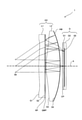
- FIG. 1 It is a figure which illustrates the structure of the peep-type wide-field image display apparatus which concerns on one Embodiment. It is a figure which illustrates the normal optical path. It is a figure which illustrates the straight optical path which can generate a ghost. It is a figure which illustrates the main ray which passes through the pupil surface S0 and has the inclination of ⁇ with respect to the optical axis A. It is a figure which illustrates the composition table about the optical system of the wide-field image display apparatus which concerns on Example 1.
- FIG. It is a figure which illustrates the coefficient of the aspherical surface equation which concerns on Example 1.
- FIG. It is a figure which illustrates the graph which shows the relationship between the focal movement and the absolute value of OTF which concerns on Example 1.
- FIG. 2 is a diagram illustrating a main ray passing through the pupil surface S0 and having an inclination of ⁇ with respect to the optical axis A in the second embodiment. It is a figure which illustrates the composition table about the optical system of the wide-field image display apparatus which concerns on Example 2.
- FIG. 2 is a diagram illustrating a main ray passing through the pupil surface S0 and having an inclination of ⁇ with respect to the optical axis A in the second embodiment.
- FIG. 2 is a diagram illustrating a graph showing the relationship between curvature of field and the viewing angle and a graph showing the relationship between percentage distortion and the viewing angle according to the second embodiment.
- FIG. 1 is a diagram illustrating a configuration of a peep-type wide-field image display device 1 according to an embodiment.
- FIG. 2 is a diagram illustrating a normal optical path.
- the wide-field image display device 1 illustrated in FIG. 1 is a wide-field image display device that is viewed by the user from the left side of FIG. 1 and used.
- the wide-field image display device 1 may be prepared for each of the user's right eye and left eye, or may be prepared only for one of the eyes. good. Further, the wide-field image display device 1 can be applied to, for example, a VR HMD.
- the wide-field image display device 1 includes an eyepiece optical system OC, a circular polarizing plate CP, and a display element D arranged in order from the user's eye side.
- the eyepiece optical system OC includes a first lens L1 and a second lens L2 arranged in order from the user's eye side.
- the first surface S1 which is the eye-side surface of the user in the first lens L1 is an aspherical surface.
- the reflective polarizing plate RP is, for example, a wire grid polarizing plate or a cholesteric polarizing plate.
- the third surface S3 may have an approximate plane around the optical axis A.
- the circular polarizing plate CP is laminated on the display element D.
- the circular polarizing plate CP is arranged in the space between the eyepiece optical system OC and the display element D (more specifically, between the half mirror HM and the display element D) without being laminated on the display element D. You may.
- the circular polarizing plate CP is, for example, a 1/4 wave plate superimposed on a linear polarizing plate.
- the display element D includes an image display surface S5 on which an image is displayed, a cover glass D1 for protecting the image display surface S5, and a display element substrate D2 for displaying an image on the image display surface S5.
- the display element D is a display panel having a large viewing angle, such as an OLED (Organic Light Emitting Diode) panel or a micro LED (Light Emitting Diode) panel.
- the image light emitted from the display element D follows the normal optical path (including the folded optical path) exemplified in FIG. 2 (and FIG. 1) as shown below, and is used. It is incident on the human eye (pupil).
- the image light emitted from the image display surface S5 of the display element D through the cover glass D1 first passes through the circular polarizing plate CP.
- the polarized state of the video light becomes a clockwise or counterclockwise circularly polarized state.
- the image light that has passed through the second lens L2 then passes through the 1/4 wave plate QWP.
- the polarization state of the video light changes from a clockwise or counterclockwise circular polarization state to a linear polarization state.
- the azimuth angle of the plane of polarization is set to 0 °.
- the image light that has passed through the 1/4 wave plate QWP is then reflected by the reflective polarizing plate RP.
- the reflective polarizing plate RP reflects the light in the linearly polarized state with an azimuth angle of 0 ° and transmits the light in the linearly polarized state with an azimuth angle of 90 °.
- the image light reflected by the reflective polarizing plate RP then passes through the 1/4 wave plate QWP again.
- the polarization state of the video light changes from the linear polarization state of the azimuth angle of 0 ° to the counterclockwise or clockwise circular polarization state.
- the image light that has passed through the 1/4 wave plate QWP then passes through the second lens L2 again in the order of the third surface S3 and the fourth surface S4. After that, a part of the video light that has passed through the fourth surface S4 of the second lens L2 is reflected by the half mirror HM, and the rest is transmitted through the half mirror HM and becomes unnecessary light.
- the video light reflected by the half mirror HM then passes through the second lens L2 again in the order of the fourth surface S4 and the third surface S3.
- the image light that has passed through the second lens L2 then passes through the 1/4 wave plate QWP again.
- the polarization state of the video light changes from the counterclockwise or clockwise circular polarization state to the linear polarization state with an azimuth angle of 90 °.
- the image light that has passed through the 1/4 wave plate QWP then passes through the reflective polarizing plate RP and passes through the first lens L1 in the order of the second surface S2 and the first surface S1. Then, the image light that has passed through the first lens L1 passes through the pupil surface S0 and is incident on the user's eye (pupil).
- the position of the pupil surface S0 is also the position of the assumed user's eye (pupil).
- the power of the eyepiece optical system OC is set to P0
- the power of the first lens L1 is set to P1
- the display element D is emitted to emit a second image light that follows the above-mentioned normal optical path.
- the power of the lens L2 is P2
- the relationship between P0 and P2 satisfies the following equation (1)
- the relationship between P1 and P2 satisfies the following equation (2).
- the optical axis A around the optical axis A on the third surface S3 of the second lens L2 is the power of the third surface S3 when the power P2 of the second lens L2 is 0.06 (unit: 1 / mm) or less.
- Is PW3, and the power due to the reflection on the user's eye side by the half mirror HM coated on the fourth surface S4 is PW4R, which is an approximate plane satisfying the following equation (3).
- the power P0 (unit: 1 / mm) of the eyepiece optical system OC satisfies the following formula (4). 0.05 ⁇ P0 ⁇ 0.075 Equation (4)
- the DD is also the diameter of the circle circumscribed by the display area of the image when the image is displayed on the image display surface S5. Further, the ED is also the diameter of a circle circumscribed by a region where the luminous flux of the image projected on the user's eye (pupil) passes through the second lens L2.
- the material of the second lens L2 is a resin material having a refractive index Nd satisfying the following formula (6) and an Abbe number Vd satisfying the following formula (7).
- Nd ⁇ 1.65 equation (6)
- Vd > 50 formula (7)
- the position of the pupil surface S0 is 12 mm from the first surface S1 of the first lens L1 toward the user's eye side, and the inclination of ⁇ with respect to the optical axis A is set to pass through the pupil surface S0.
- the main ray of possession is reversely tracked from the pupil surface S0 toward the first surface S1
- the main ray first incident on the third surface S3 of the second lens L2 is the optical axis A in the traveling direction.
- the main light ray emitted from the fourth surface S4 of the second lens L2 is inclined in a direction away from the optical axis A in the traveling direction.
- the angle of incidence of the main ray first incident on the third surface S3 with respect to the third surface S3 is set to ⁇ 3, and the fourth surface S4 of the main ray emitting out the fourth surface S4.
- ⁇ 3 satisfies the following equation (8)
- ⁇ 4 satisfies the following equation (9).
- the power P2 of the second lens L2 can be approximately obtained by the following equation (10).
- the power elements of PW4, PW3_1, PW3_2, PW4R, and PW3_3 are as follows. Note that PW3_1, PW3_2, and PW3_3 have the same value PW3.
- PW4 is the power due to refraction on the fourth surface S4 when the video light passing through the circular polarizing plate CP and passing through the half mirror HM is incident on the fourth surface S4.
- PW3_1 is the power due to refraction on the third surface S3 when the video light incident on the fourth surface S4 passes through the half mirror HM and exits the third surface S3.
- PW3_2 is the power due to bending on the third surface S3 when the image light reflected by the reflective polarizing plate RP and passing through the 1/4 wave plate QWP is incident on the third surface S3.
- the PW4R is the power generated by the reflection of the video light incident on the third surface S3 when it is reflected by the half mirror HM. This power can be calculated by the following equation (11-3) using the optical formula.
- PW3_3 is the power due to refraction on the third surface S3 when the image light reflected by the half mirror HM and incident on the fourth surface S4 exits the third surface S3.
- PW4 can be calculated by the following equation (11-1) using the optical formula.
- PW4 (1-Nd) ⁇ C4 equation (11-1)
- Nd is the refractive index of the second lens L2
- C4 is the curvature of the fourth surface S4.
- PW3_1, PW3_2, and PW3_3 have the same value PW3.
- This power can be calculated by the following equation (11-2) using the optical formula.
- PW3 (Nd-1) ⁇ C3 equation (11-2)
- C3 is the curvature of the third surface S3.
- PW4R can be calculated by the following equation (11-3) using the optical formula.
- PW4R -2 x Nd x C4 formula (11-3)
- each power element on the right side of the above equation (10) has a positive value. From this, the power that the second lens L2 needs to bear is obtained by synthesizing relatively small power elements.
- the fourth surface S4 can produce a PW4R of a required size with a particularly loose curvature.
- the second lens L2 is composed of a convex surface having a loose curvature, and can generate a large power satisfying the above equations (1) and (4), so that the occurrence of aberration can be suppressed to a small extent.
- the second lens L2 can produce the required power even if the lens is made of a material having a relatively small refractive index Nd. Therefore, as the material of the second lens L2, a material having a large Abbe number Vd, that is, a material having a small dispersion can be selected. By selecting a material having a small dispersion, the occurrence of chromatic aberration of the second lens L2 can be suppressed to a low level.
- the material of the second lens L2 is preferably selected from the materials included in the range satisfying the above formulas (6) and (7). Then, by selecting the injection-moldable resin material included in this range, the second lens L2 can be manufactured easily and at low cost.
- the third surface S3 of the second lens L2 and the first surface S1 of the first lens L1 are both aspherical surfaces and face the air, they have a large aberration correction effect.
- the surface can correct the aberration of the entire OC of the eyepiece optical system to a practically sufficient level.
- the power of the second lens L2 is almost the same as the power P0 of the eyepiece lens, that is, the second lens L2.
- the power required for the lens may be 0.06 (unit: 1 / mm) or less.
- this power is a magnitude that can be reasonably produced only by PW4R calculated by the above equation (11-3).
- the third surface S3, which is an aspherical surface may be an approximate plane whose shape around the optical axis A is close to a plane as long as the above equation (3) is satisfied.
- the above equation (12) can be expressed as the following equation (13), and the power P1 of the first lens L1 has a negative value.
- the above equation (12) can be expressed as the following equation (14).
- the power P0 of the eyepiece optical system OC is increased in order to create a large FOV from the small display element D, the focal length becomes shorter. Therefore, sufficient eye relief is secured for the eyepiece optical system OC and the display element D is used. In order to secure the distance, it is important to satisfy the above equations (13) and (14) as described below.
- the focal length of the eyepiece OC is as short as less than 20 mm, and therefore, when the power of the first lens L1 exceeds a certain value, it becomes difficult to secure eye relief.
- the rear side of the eyepiece optical system OC is obtained.
- the focal position moves toward the inside of the eyepiece optical system OC. Therefore, when the positive power of the first lens L1 with respect to the second lens L2 exceeds a certain limit, the posterior focal position slips into the inside of the eyepiece optical system OC. Since it is necessary to project a virtual image from a distance, it is necessary to arrange the image display surface S5 of the display element D near the focal position on the rear side of the eyepiece optical system OC.
- the posterior focal position of the eyepiece optical system OC is located on the outer side of the eyepiece optical system OC (in FIG. 1 or FIG. 2) with respect to the fourth surface S4 of the second lens L2. Must be on the right side of).
- the first lens L1 has a negative power
- the stronger the negative power of the first lens L1 the larger the luminous flux diameter of the image light passing through the second lens L2.
- the second lens L2 needs to cancel the negative power of the first lens L1, it is necessary to strengthen the positive power. Therefore, when the negative power of the first lens L1 exceeds a certain limit, the image peripheral light that should pass through the second lens L2 and head toward the display element D is the fourth lens L2 of the second lens L2. Total internal reflection occurs on the surface S4.
- the second surface S2 is a plane or an approximate plane
- the first surface S1 is an aspherical surface.
- This aspherical surface becomes stronger toward the outer periphery in the negative direction in order to correct the tangier field curvature generated in the negative direction in the second lens L2, and therefore, in a particularly large FOV, the first The outer periphery of the surface S1 protrudes toward the user's eye (see, for example, FIG. 1).
- the stronger the negative power of the first lens L1 the larger the amount of protrusion thereof, and the more likely it is that interference with the user's face occurs.
- the first surface S1 is an aspherical surface and has an important function of canceling the aberration generated in the second lens L2.
- the power is not appropriately set. There arises a problem that sufficient eye relief cannot be secured and the distance between the second lens L2 and the display element D cannot be secured.
- these problems can be avoided by satisfying the above equations (13) and (14).
- the first lens L1 is thin and has little eye relief loss.
- the second surface S2 of the first lens L1 is a plane or an approximate plane, even if the reflective polarizing plate RP and the 1/4 wave plate QWP are laminated on the surface, the surface may be laminated. The adhesion can be kept good.
- the diameter of the laminated surface of the second surface S2 on which the reflective polarizing plate RP and the 1/4 wave plate QWP are laminated is DL, and the maximum value of the sag of the second surface S2 is SL, it is a plane or an approximate plane.
- the second surface S2 is a plane, a spherical surface, or an aspherical surface satisfying the following equation (16). 0.05 ⁇ DL >
- the four-wavelength film) QWP can be laminated on the second surface S2 by expanding and contracting the circumferential dimension by about 0.6%. This degree of expansion and contraction is a reasonable value if it is a reflective polarizing plate (reflection polarizing film) RP and a 1/4 wave plate (1/4 wave film) QWP using a resin film as a base material.
- FIG. 3 is a diagram illustrating straight light.
- the straight light is light that emits the display element D and passes through the pupil S0 without following the normal optical path (that is, never reflecting) as illustrated in FIG. 2 (and FIG. 1), and generates a ghost. It is a stray light to get.
- the second lens L2 is made of a material having a small birefringence, and since the retardation is proportional to the birefringence and the optical path length, the internal stress remains and the birefringence is caused by the photoelastic effect. It is important to shorten the optical path length of the peripheral portion of the lens, which tends to appear frequently, and the second lens L2, in which both the third surface S3 and the fourth surface S4 have a convex shape, has a shape suitable for this. There is.
- the straight light that emits the display element D passes through the eyepiece optical system OC without being reflected even once, and passes through the pupil S0, including the dependent light beam, is the display element. It is convergent light from D toward the user's eye side, and the size of the passing region in the second lens L2 of this light beam is smaller than the size of the image displayed on the image display surface S5.
- the straight light emitted from the image display surface S5 and passing through the pupil surface S0 causes the second lens L2 to have a large birefringence. Avoid the surrounding area and pass through. From this, the permissible amount of birefringence in the peripheral portion of the second lens L2 can be greatly relaxed.
- the retardation is preferably 10 nm or less in the central portion of the second lens L2, but there is no problem even if the peripheral portion is about several tens of nm.
- the third surface S3 of the second lens L2 is an aspherical surface
- molding is preferable as the manufacturing method in consideration of mass productivity.
- thermal stress remains in the peripheral portion of the lens, and there is a strong tendency for birefringence to increase due to the photoelastic effect.
- the resin material used at this time include Optimas (registered trademark) of Mitsubishi Gas Chemicals, Inc., AZP (registered trademark) announced by Asahi Kasei Corporation in 2014, APEL (registered trademark) of Mitsui Chemicals, Inc., etc.
- Resin materials such as can be used. All of these are acrylic materials satisfying the above formulas (6) and (7).
- the wide-field image display device 1 satisfies the above equation (4).
- the reason why the power P0 of the eyepiece optical system OC is less than 0.075 (unit: 1 / mm) is that the second lens L2 can produce strong power with a single lens, but the stronger the power, the more aberrations increase. This is because the aberration becomes remarkably large especially when it exceeds 0.075 (unit: 1 / mm).
- the power of the optical system OC is 0.05 (unit: 1 / mm) or less, the DD (maximum size of the image displayed on the image display surface S5) on the left side in the above equation (5) becomes too large. This is because it becomes difficult to satisfy the above equation (5).
- EFL is the focal length of the eyepiece optical system OC.
- Dis (unit:%) is a percentage distortion at the image edge portion of the eyepiece optical system OC defined by the following formula (18).
- Dis (actual maximum image height-ideal maximum image height) / (ideal maximum image height) x 100 equation (18) FOV is the viewing angle of the eyepiece optical system OC.
- DD the maximum size of the image displayed on the image display surface S5.
- DD / 2 is the image height of the image.
- an eyepiece optical system having a negative Dis can reduce the power of the eyepiece optical system as compared with an eyepiece optical system without a Dis. For example, if Dis is -30%, the power of the eyepiece optical system can be reduced by 30% as compared with the case without Dis.
- the power of the eyepiece optical system OC and the power of the second lens L2 are substantially the same, it can be said that the power of the second lens L2 can be reduced by about 30%.
- the second lens L2 can produce a strong power, but the stronger the power, the larger the aberration. Therefore, in order to obtain excellent resolution performance, it is preferable that the power of the second lens L2 is small. In particular, when the power of the second lens L2 is 0.075 (unit: 1 / mm) or more, the aberration becomes remarkably large.
- the negative Dis can realize the eyepiece optical system OC with higher resolution performance while maintaining the FOV.
- the negative Dis can realize a larger FOV eyepiece optical system OC while maintaining the resolution performance.
- the position of the pupil surface S0 is assumed to be a position 12 mm from the first surface S1 of the first lens L1, and the optical axis A passes through the pupil surface S0.
- the main ray having an inclination of ⁇ is reversely tracked from the pupil surface S0 toward the first surface S1
- the main ray first incident on the third surface S3 of the second lens L2 travels in the traveling direction.
- the main light ray emitted from the fourth surface S4 of the second lens L2 is inclined toward the optical axis A toward the direction of travel toward the optical axis A.
- FIG. 4 is a diagram illustrating a main ray passing through the pupil surface S0 and having an inclination of ⁇ with respect to the optical axis A.
- the main ray CR4 emitted from the fourth surface S4 of the second lens L2 travels in the traveling direction. Since the fourth surface S4 is inclined toward the optical axis A and has a convex shape toward the display element D, the emission angle ⁇ 4 from the fourth surface S4 of the main ray CR4 is clockwise. Has a large angle. For this reason, a large negative spherical aberration is generated in the main ray on the fourth surface S4.
- the main ray CR3 first incident on the third surface S3 of the second lens is inclined in a direction away from the optical axis A in the traveling direction, and the third surface S3 is used around the optical axis A. Since it has a convex shape or an approximate plane toward the eye of a person, the angle of incidence ⁇ 3 of the main ray CR3 on the third surface S3 has a clockwise angle. For this reason, negative spherical aberration is generated in the main ray on the third surface S3. In particular, when the third surface S3 has a convex shape toward the eye of the user, the incident angle ⁇ 3 becomes large, and a large negative spherical aberration occurs.
- the height of the main light beam emitted at 40 °) across the image display surface S5 of the display element D can be lowered. That is, the action of creating a negative Dis is born. As described above, this is preferable for designing a large FOV eyepiece optical system OC while maintaining the resolution performance.
- the position of the pupil surface S0 is assumed to be 12 mm from the first surface S1 of the first lens L1 is that ⁇ 3 and ⁇ 4 change when the position of the pupil surface S0 changes, so that ⁇ 3 and ⁇ 4 This is because it is necessary to assume the position of the pupil surface S0 in order to quantitatively define.
- the spectacles are adjusted so that the distance between the eye and the spectacle lens is 12 mm. This is to prevent the spectacle lens from being soiled by the splash of tears generated by blinking. Even in the wide-field image display device 1, it is preferable to increase the distance between the eyepiece optical system OC and the eye by 12 mm or more.
- the third surface S3 of the second lens L2 has a convex shape or an approximate plane
- the fourth surface S4 has a convex shape. It has substantially five positive power elements (see equation (10) above) due to the folded optical path created by utilizing polarization and reflection.
- the second lens L2 can generate a strong positive power on a convex surface having a gentle curvature, and can suppress the occurrence of aberration.
- a sufficiently strong positive power can be produced by using a material having a low refractive index, a material having a low dispersion can be selected and the occurrence of chromatic aberration can be suppressed.
- first surface S1 of the first lens L1 and the third surface S3 of the second lens L2 are aspherical surfaces facing the air, and the fact that they face the air means that their interfaces are refracted. Since the rate difference is large, the first surface S1 and the third surface S3 can strongly correct aberrations even if they have a relatively gentle aspherical shape. Therefore, it is possible to design an eyepiece optical system OC having excellent resolving power, and it is possible to reduce the sag and make the eyepiece optical system OC thinner.
- both the third surface S3 and the fourth surface S4 of the second lens L2 have a convex shape, a large incident angle ⁇ 3 and an emission angle ⁇ 4 of the main ray can be obtained, and negative image distortion is obtained in the reverse tracking. To create. As a result, a large FOV image can be projected from the display element D having a small image display surface size while suppressing the power of the second lens L2. Further, the size of the image display surface can be designed to be smaller than the outer diameter of the second lens L2.
- the stray light traveling straight in the eyepiece optical system OC travels in the second lens L2 while avoiding the peripheral portion of the lens where birefringence is likely to occur, and thus the compound in the outer peripheral portion of the second lens L2.
- the allowable amount of refraction can be increased, and the second lens L2 can be manufactured by molding the resin. According to the molding, even an aspherical lens can be manufactured at low cost.
- the power distribution between the first lens L1 and the second lens L2 enables a design that secures sufficient eye relief and avoids buffering between the eyepiece optical system OC and the display element D.
- a wide-field (FOV of 80 ° or more) and high-resolution images can be visually recognized by the user, and the image is compact (thin) and lightweight. The effects of excellent mass productivity and low manufacturing cost can be obtained.
- the case where the optical axis A of the third surface S3 of the second lens L2 is convex toward the user's eyes is specified.
- An example is shown as Example 1
- a specific example in the case where the optical axis A of the third surface S3 of the second lens L2 is an approximate plane is shown as Example 2.
- the configuration table shown in each embodiment is numbered serially in the direction of tracing the optical path of the video light in the reverse direction. Further, in each embodiment, the optical specifications and the performance are shown by tracing the optical path in the reverse direction in view of the law of light reversal.
- the material of the second lens L2 is Optimas (registered trademark) 7500 of Mitsubishi Gas Chemical Company, Inc.
- the wide-field image display device 1 has an inclination of ⁇ (40 °) with respect to the optical axis A through its configuration, a normal optical path, a straight optical path capable of generating a ghost, and a pupil surface S0.
- the main ray is the same as that shown in FIGS. 1, 2, 3, and 4.
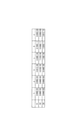
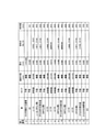
- FIG. 5 is a diagram illustrating a configuration table relating to an optical system of the wide-field image display device 1 according to the first embodiment.
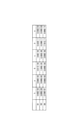
- FIG. 6 is a diagram illustrating the coefficients of the aspherical equation according to the first embodiment.
- the configuration table exemplified in FIG. 5 shows the type of the surface corresponding to each serial number, the radius of curvature around the optical axis A, the thickness around the optical axis A, the material (Nd, Vd), and the effective diameter.
- the sag of each aspherical surface can be obtained by the aspherical equation of the following equation (23).
- Y (unit: mm) is a distance from the optical axis A.
- R (unit: mm) is the radius of curvature around the optical axis A.
- Sag (unit: mm) is the coordinates in the optical axis A direction when the center of the optical axis of the surface in Y is the origin.
- the coefficients k, a, b, c, d, and e for each aspherical surface are as shown in FIG.
- P0, P1, P2, PW3, and PW4R are as follows.
- the above equations (1) and (2) are satisfied, and the above equation (4) is also satisfied.
- the material of the second lens L2 is Optimas (registered trademark) 7500 of Mitsubishi Gas Chemical Company, Inc., which also satisfies the above formulas (6) and (7).
- the FOV, DD, Dis, ⁇ 3, and ⁇ 4 are as follows.
- the DD is 22.8 mm
- the above formula (5) is also satisfied from the effective diameter of the second lens L2 in the configuration table shown in FIG. Further, since ⁇ 3 is 42.9 ° and ⁇ 4 is 35.3 °, both the above equations (8) and (9) are satisfied.
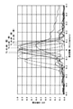
- FIG. 7 a graph showing the relationship between the focal movement and the absolute value of the OTF (Optical Transfer Function) is illustrated in FIG. 7, and the relationship between the curvature of field and the viewing angle is illustrated.
- FIG. 8 exemplifies a graph showing the above and a graph showing the relationship between the percentage distortion and the viewing angle.
- the graph illustrated in FIG. 7 is for a case where the spatial frequency is 40 cycles / mm, the wavelength is 525 ⁇ m, the pupil diameter is 4 mm, and the pupil position is 15 mm.
- the graph illustrated in FIG. 8 is for the case where the pupil position is 15 mm. Both graphs show that the resolution performance of the eyepiece optical system OC according to the first embodiment is good.
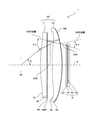
- FIG. 9 is a diagram illustrating the configuration of the wide-field video display device 1 according to the second embodiment.
- FIG. 10 is a diagram illustrating a normal optical path according to the second embodiment.
- FIG. 11 is a diagram illustrating a straight optical path capable of generating a ghost according to the second embodiment.
- FIG. 12 is a diagram illustrating a main ray passing through the pupil surface S0 and having an inclination of ⁇ with respect to the optical axis A in the second embodiment.
- the optical axis A of the third surface S3 of the second lens L2 is an approximate plane.
- the normal optical path becomes an optical path as exemplified in FIG. 10 (and FIG. 9), and the straight optical path capable of generating a ghost becomes an optical path as exemplified in FIG.
- the main ray passing through the pupil surface S0 and having an inclination of ⁇ (40 °) with respect to the optical axis A is as illustrated in FIG.
- FIG. 13 is a diagram illustrating a configuration table relating to an optical system of the wide-field image display device 1 according to the second embodiment.
- FIG. 14 is a diagram illustrating the coefficients of the aspherical equation according to the second embodiment.
- the sag of each aspherical surface can be obtained by the aspherical surface equation of the above equation (23).
- the coefficients k, a, b, c, d, and e for each aspherical surface are as shown in FIG.
- P0, P1, P2, PW3, and PW4R are as follows.
- P2 0.94 x P0,
- 0.16 ⁇ P2,
- P2 0.06 (unit: 1 / mm) or less, and from each value of PW3 and PW4R, the circumference of the optical axis A on the third surface S3 is an approximate plane satisfying the above equation (3). It has become.
- the material of the second lens L2 is Optimas (registered trademark) 7500 of Mitsubishi Gas Chemical Company, Inc., as in Example 1, and the above formulas (6) and (7) are also satisfied.
- the FOV, DD, Dis, ⁇ 3, and ⁇ 4 are as follows.
- the DD is 12.0 mm
- the above formula (5) is also satisfied from the effective diameter of the second lens L2 in the configuration table exemplified in FIG. Further, since ⁇ 3 is 38.4 ° and ⁇ 4 is 28.3 °, the above formula (8) is satisfied although the above formula (9) is not satisfied.
- FIG. 15 a graph showing the relationship between the focal movement and the absolute value of OTF is illustrated in FIG. 15, and the graph showing the relationship between the curvature of field and the viewing angle and the percentage are shown.
- a graph showing the relationship between the distortion and the viewing angle is illustrated in FIG.
- the graph illustrated in FIG. 15 is for a case where the spatial frequency is 40 cycles / mm, the wavelength is 525 ⁇ m, the pupil diameter is 4 mm, and the pupil position is 15 mm.
- the graph illustrated in FIG. 16 is for the case where the pupil position is 15 mm. Both graphs show that the resolution performance of the eyepiece optical system OC according to the second embodiment is good.
- the present invention is not limited to the above embodiment as it is, and at the implementation stage, the components can be modified and embodied within a range that does not deviate from the gist thereof.
- various inventions can be formed by an appropriate combination of the plurality of components disclosed in the above-described embodiment. For example, some components of all the components shown in the embodiment may be deleted. In addition, components across different embodiments may be combined as appropriate.
Landscapes
- Physics & Mathematics (AREA)
- General Physics & Mathematics (AREA)
- Optics & Photonics (AREA)
- Engineering & Computer Science (AREA)
- Multimedia (AREA)
- Signal Processing (AREA)
- Lenses (AREA)
Priority Applications (4)
| Application Number | Priority Date | Filing Date | Title |
|---|---|---|---|
| CN202080103333.0A CN115917375B (zh) | 2020-08-21 | 2020-08-21 | 宽视野影像显示装置 |
| PCT/JP2020/031665 WO2022038777A1 (ja) | 2020-08-21 | 2020-08-21 | 広視野映像表示装置 |
| JP2022543249A JP7692421B2 (ja) | 2020-08-21 | 2020-08-21 | 広視野映像表示装置 |
| US18/021,975 US12523875B2 (en) | 2020-08-21 | 2020-08-21 | Wide-field video display apparatus |
Applications Claiming Priority (1)
| Application Number | Priority Date | Filing Date | Title |
|---|---|---|---|
| PCT/JP2020/031665 WO2022038777A1 (ja) | 2020-08-21 | 2020-08-21 | 広視野映像表示装置 |
Publications (1)
| Publication Number | Publication Date |
|---|---|
| WO2022038777A1 true WO2022038777A1 (ja) | 2022-02-24 |
Family
ID=80322642
Family Applications (1)
| Application Number | Title | Priority Date | Filing Date |
|---|---|---|---|
| PCT/JP2020/031665 Ceased WO2022038777A1 (ja) | 2020-08-21 | 2020-08-21 | 広視野映像表示装置 |
Country Status (4)
| Country | Link |
|---|---|
| US (1) | US12523875B2 (https=) |
| JP (1) | JP7692421B2 (https=) |
| CN (1) | CN115917375B (https=) |
| WO (1) | WO2022038777A1 (https=) |
Cited By (8)
| Publication number | Priority date | Publication date | Assignee | Title |
|---|---|---|---|---|
| CN114675419A (zh) * | 2022-03-16 | 2022-06-28 | 江西凤凰光学科技有限公司 | 一种近眼型虚拟现实光学模组 |
| CN116755250A (zh) * | 2023-05-15 | 2023-09-15 | 华勤技术股份有限公司 | 一种光学系统 |
| WO2023221239A1 (zh) * | 2022-05-19 | 2023-11-23 | 歌尔光学科技有限公司 | 光学模组以及头戴显示设备 |
| WO2024014202A1 (ja) * | 2022-07-15 | 2024-01-18 | ソニーグループ株式会社 | 光学系及び表示装置 |
| CN119270395A (zh) * | 2023-07-07 | 2025-01-07 | 北京字跳网络技术有限公司 | 透镜组件、显示模组和电子设备 |
| WO2025081978A1 (zh) * | 2023-10-19 | 2025-04-24 | 歌尔光学科技有限公司 | 近眼光学系统以及头戴显示设备 |
| EP4468060A4 (en) * | 2022-07-04 | 2025-06-04 | Samsung Electronics Co., Ltd. | HABITRONIC ELECTRONIC DEVICE COMPRISING A LENS ASSEMBLY |
| US12405474B2 (en) | 2023-05-22 | 2025-09-02 | Canon Kabushiki Kaisha | Optical system and image display apparatus |
Families Citing this family (3)
| Publication number | Priority date | Publication date | Assignee | Title |
|---|---|---|---|---|
| JP7600756B2 (ja) * | 2021-02-26 | 2024-12-17 | セイコーエプソン株式会社 | 光学ユニット及び画像表示装置 |
| US20250138308A1 (en) * | 2022-02-09 | 2025-05-01 | Sony Group Corporation | Optical system and display device |
| CN116974073A (zh) * | 2022-11-10 | 2023-10-31 | 诚瑞光学(常州)股份有限公司 | 光学系统 |
Citations (4)
| Publication number | Priority date | Publication date | Assignee | Title |
|---|---|---|---|---|
| JP2019053152A (ja) * | 2017-09-14 | 2019-04-04 | セイコーエプソン株式会社 | 虚像表示装置 |
| US20200053350A1 (en) * | 2018-08-10 | 2020-02-13 | Valve Corporation | Head-mounted display (hmd) with spatially-varying retarder optics |
| JP2020095205A (ja) * | 2018-12-14 | 2020-06-18 | キヤノン株式会社 | 画像表示装置、及び、接眼光学系 |
| JP2020519964A (ja) * | 2017-05-16 | 2020-07-02 | スリーエム イノベイティブ プロパティズ カンパニー | 光学システム |
Family Cites Families (13)
| Publication number | Priority date | Publication date | Assignee | Title |
|---|---|---|---|---|
| US9557568B1 (en) * | 2015-09-03 | 2017-01-31 | 3M Innovative Properties Company | Head-mounted display |
| CN106526851B (zh) * | 2016-09-29 | 2019-02-01 | 玉晶光电(厦门)有限公司 | 目镜光学系统 |
| CN106526852B (zh) * | 2016-09-29 | 2019-05-03 | 玉晶光电(厦门)有限公司 | 目镜光学系统 |
| CN106444046A (zh) * | 2016-12-14 | 2017-02-22 | 浙江舜通智能科技有限公司 | 一种光学系统及装配该光学系统的头戴式显示装置 |
| CN110088672A (zh) * | 2016-12-20 | 2019-08-02 | 3M创新有限公司 | 光学系统 |
| US11181731B1 (en) * | 2017-01-02 | 2021-11-23 | Kopin Corporation | Wide field of view (WFOV) optical system and method |
| WO2018163035A1 (en) | 2017-03-08 | 2018-09-13 | 3M Innovative Properties Company | Optical system |
| JP7077656B2 (ja) * | 2018-02-26 | 2022-05-31 | セイコーエプソン株式会社 | 虚像表示装置 |
| CN108303796B (zh) * | 2018-04-09 | 2020-07-28 | 浙江舜宇光学有限公司 | 目镜 |
| JP7154878B2 (ja) * | 2018-08-22 | 2022-10-18 | キヤノン株式会社 | 観察光学系及びそれを有する観察装置 |
| JP2020095073A (ja) * | 2018-12-10 | 2020-06-18 | キヤノン株式会社 | 観察光学系及びそれを有する観察装置 |
| CN110308559A (zh) * | 2019-06-28 | 2019-10-08 | 上海视涯信息科技有限公司 | 一种虚拟现实光学模组及虚拟现实设备 |
| CN111443491A (zh) * | 2020-04-30 | 2020-07-24 | 京东方科技集团股份有限公司 | 一种光学显示系统及控制方法、显示装置 |
-
2020
- 2020-08-21 CN CN202080103333.0A patent/CN115917375B/zh active Active
- 2020-08-21 JP JP2022543249A patent/JP7692421B2/ja active Active
- 2020-08-21 WO PCT/JP2020/031665 patent/WO2022038777A1/ja not_active Ceased
- 2020-08-21 US US18/021,975 patent/US12523875B2/en active Active
Patent Citations (4)
| Publication number | Priority date | Publication date | Assignee | Title |
|---|---|---|---|---|
| JP2020519964A (ja) * | 2017-05-16 | 2020-07-02 | スリーエム イノベイティブ プロパティズ カンパニー | 光学システム |
| JP2019053152A (ja) * | 2017-09-14 | 2019-04-04 | セイコーエプソン株式会社 | 虚像表示装置 |
| US20200053350A1 (en) * | 2018-08-10 | 2020-02-13 | Valve Corporation | Head-mounted display (hmd) with spatially-varying retarder optics |
| JP2020095205A (ja) * | 2018-12-14 | 2020-06-18 | キヤノン株式会社 | 画像表示装置、及び、接眼光学系 |
Cited By (9)
| Publication number | Priority date | Publication date | Assignee | Title |
|---|---|---|---|---|
| CN114675419A (zh) * | 2022-03-16 | 2022-06-28 | 江西凤凰光学科技有限公司 | 一种近眼型虚拟现实光学模组 |
| CN114675419B (zh) * | 2022-03-16 | 2023-06-13 | 江西凤凰光学科技有限公司 | 一种近眼型虚拟现实光学模组 |
| WO2023221239A1 (zh) * | 2022-05-19 | 2023-11-23 | 歌尔光学科技有限公司 | 光学模组以及头戴显示设备 |
| EP4468060A4 (en) * | 2022-07-04 | 2025-06-04 | Samsung Electronics Co., Ltd. | HABITRONIC ELECTRONIC DEVICE COMPRISING A LENS ASSEMBLY |
| WO2024014202A1 (ja) * | 2022-07-15 | 2024-01-18 | ソニーグループ株式会社 | 光学系及び表示装置 |
| CN116755250A (zh) * | 2023-05-15 | 2023-09-15 | 华勤技术股份有限公司 | 一种光学系统 |
| US12405474B2 (en) | 2023-05-22 | 2025-09-02 | Canon Kabushiki Kaisha | Optical system and image display apparatus |
| CN119270395A (zh) * | 2023-07-07 | 2025-01-07 | 北京字跳网络技术有限公司 | 透镜组件、显示模组和电子设备 |
| WO2025081978A1 (zh) * | 2023-10-19 | 2025-04-24 | 歌尔光学科技有限公司 | 近眼光学系统以及头戴显示设备 |
Also Published As
| Publication number | Publication date |
|---|---|
| JPWO2022038777A1 (https=) | 2022-02-24 |
| US12523875B2 (en) | 2026-01-13 |
| CN115917375B (zh) | 2025-10-24 |
| JP7692421B2 (ja) | 2025-06-13 |
| US20230359033A1 (en) | 2023-11-09 |
| CN115917375A (zh) | 2023-04-04 |
Similar Documents
| Publication | Publication Date | Title |
|---|---|---|
| WO2022038777A1 (ja) | 広視野映像表示装置 | |
| CN110196492B (zh) | 虚像显示装置 | |
| JP2020095205A (ja) | 画像表示装置、及び、接眼光学系 | |
| CN110196493A (zh) | 虚像显示装置 | |
| JP2020020858A (ja) | 虚像表示装置 | |
| JP2006003872A (ja) | 光学素子、コンバイナ光学系、及び情報表示装置 | |
| CN116974038A (zh) | 光学透镜组及头戴式电子装置 | |
| US20180373038A1 (en) | Optics of wearable display devices | |
| TWI852539B (zh) | 光學透鏡組和頭戴式電子裝置 | |
| TWI856640B (zh) | 光學透鏡組和頭戴式電子裝置 | |
| JP7183610B2 (ja) | 虚像表示装置 | |
| WO2024143534A1 (ja) | 接眼光学系、広視野映像表示装置 | |
| JP2001142025A (ja) | 画像表示装置 | |
| CN118050896A (zh) | 光学镜头模块、光机模块以及头戴式显示装置 | |
| CN116626895A (zh) | 虚像显示装置用光学系统、虚像显示装置及头戴式显示器 | |
| JP2016170203A (ja) | 画像表示装置 | |
| TWI875059B (zh) | 光學透鏡組和電子裝置 | |
| JP2006091477A (ja) | ホログラフィック反射面を有する広角観察光学系 | |
| CN116880074B (zh) | 虚拟现实装置 | |
| CN115685550A (zh) | 虚像显示装置 | |
| JP7799745B2 (ja) | 表示光学系および表示装置 | |
| CN117850011B (zh) | 光学成像系统及包括该光学成像系统的vr设备 | |
| TWI829434B (zh) | 光學鏡頭模組、光機模組以及頭戴式顯示裝置 | |
| WO2024202601A1 (ja) | 光学系及び表示装置 | |
| WO2025141916A1 (ja) | 光学系及び表示装置 |
Legal Events
| Date | Code | Title | Description |
|---|---|---|---|
| 121 | Ep: the epo has been informed by wipo that ep was designated in this application |
Ref document number: 20950342 Country of ref document: EP Kind code of ref document: A1 |
|
| ENP | Entry into the national phase |
Ref document number: 2022543249 Country of ref document: JP Kind code of ref document: A |
|
| NENP | Non-entry into the national phase |
Ref country code: DE |
|
| 122 | Ep: pct application non-entry in european phase |
Ref document number: 20950342 Country of ref document: EP Kind code of ref document: A1 |
|
| WWG | Wipo information: grant in national office |
Ref document number: 202080103333.0 Country of ref document: CN |
|
| WWG | Wipo information: grant in national office |
Ref document number: 18021975 Country of ref document: US |