WO2022034862A1 - 表示装置、表示装置の製造方法、並びに、表示装置を用いた電子機器 - Google Patents
表示装置、表示装置の製造方法、並びに、表示装置を用いた電子機器 Download PDFInfo
- Publication number
- WO2022034862A1 WO2022034862A1 PCT/JP2021/029374 JP2021029374W WO2022034862A1 WO 2022034862 A1 WO2022034862 A1 WO 2022034862A1 JP 2021029374 W JP2021029374 W JP 2021029374W WO 2022034862 A1 WO2022034862 A1 WO 2022034862A1
- Authority
- WO
- WIPO (PCT)
- Prior art keywords
- display device
- layer
- upper electrode
- light emitting
- inter
- Prior art date
- Legal status (The legal status is an assumption and is not a legal conclusion. Google has not performed a legal analysis and makes no representation as to the accuracy of the status listed.)
- Ceased
Links
Images














Classifications
-
- H—ELECTRICITY
- H10—SEMICONDUCTOR DEVICES; ELECTRIC SOLID-STATE DEVICES NOT OTHERWISE PROVIDED FOR
- H10K—ORGANIC ELECTRIC SOLID-STATE DEVICES
- H10K59/00—Integrated devices, or assemblies of multiple devices, comprising at least one organic light-emitting element covered by group H10K50/00
- H10K59/10—OLED displays
- H10K59/12—Active-matrix OLED [AMOLED] displays
- H10K59/122—Pixel-defining structures or layers, e.g. banks
-
- G—PHYSICS
- G09—EDUCATION; CRYPTOGRAPHY; DISPLAY; ADVERTISING; SEALS
- G09F—DISPLAYING; ADVERTISING; SIGNS; LABELS OR NAME-PLATES; SEALS
- G09F9/00—Indicating arrangements for variable information in which the information is built-up on a support by selection or combination of individual elements
-
- G—PHYSICS
- G09—EDUCATION; CRYPTOGRAPHY; DISPLAY; ADVERTISING; SEALS
- G09F—DISPLAYING; ADVERTISING; SIGNS; LABELS OR NAME-PLATES; SEALS
- G09F9/00—Indicating arrangements for variable information in which the information is built-up on a support by selection or combination of individual elements
- G09F9/30—Indicating arrangements for variable information in which the information is built-up on a support by selection or combination of individual elements in which the desired character or characters are formed by combining individual elements
-
- H—ELECTRICITY
- H05—ELECTRIC TECHNIQUES NOT OTHERWISE PROVIDED FOR
- H05B—ELECTRIC HEATING; ELECTRIC LIGHT SOURCES NOT OTHERWISE PROVIDED FOR; CIRCUIT ARRANGEMENTS FOR ELECTRIC LIGHT SOURCES, IN GENERAL
- H05B33/00—Electroluminescent light sources
- H05B33/02—Details
-
- H—ELECTRICITY
- H05—ELECTRIC TECHNIQUES NOT OTHERWISE PROVIDED FOR
- H05B—ELECTRIC HEATING; ELECTRIC LIGHT SOURCES NOT OTHERWISE PROVIDED FOR; CIRCUIT ARRANGEMENTS FOR ELECTRIC LIGHT SOURCES, IN GENERAL
- H05B33/00—Electroluminescent light sources
- H05B33/02—Details
- H05B33/04—Sealing arrangements, e.g. against humidity
-
- H—ELECTRICITY
- H05—ELECTRIC TECHNIQUES NOT OTHERWISE PROVIDED FOR
- H05B—ELECTRIC HEATING; ELECTRIC LIGHT SOURCES NOT OTHERWISE PROVIDED FOR; CIRCUIT ARRANGEMENTS FOR ELECTRIC LIGHT SOURCES, IN GENERAL
- H05B33/00—Electroluminescent light sources
- H05B33/10—Apparatus or processes specially adapted to the manufacture of electroluminescent light sources
-
- H—ELECTRICITY
- H05—ELECTRIC TECHNIQUES NOT OTHERWISE PROVIDED FOR
- H05B—ELECTRIC HEATING; ELECTRIC LIGHT SOURCES NOT OTHERWISE PROVIDED FOR; CIRCUIT ARRANGEMENTS FOR ELECTRIC LIGHT SOURCES, IN GENERAL
- H05B33/00—Electroluminescent light sources
- H05B33/12—Light sources with substantially two-dimensional [2D] radiating surfaces
-
- H—ELECTRICITY
- H05—ELECTRIC TECHNIQUES NOT OTHERWISE PROVIDED FOR
- H05B—ELECTRIC HEATING; ELECTRIC LIGHT SOURCES NOT OTHERWISE PROVIDED FOR; CIRCUIT ARRANGEMENTS FOR ELECTRIC LIGHT SOURCES, IN GENERAL
- H05B33/00—Electroluminescent light sources
- H05B33/12—Light sources with substantially two-dimensional [2D] radiating surfaces
- H05B33/22—Light sources with substantially two-dimensional [2D] radiating surfaces characterised by the chemical or physical composition or the arrangement of auxiliary dielectric or reflective layers
-
- H—ELECTRICITY
- H05—ELECTRIC TECHNIQUES NOT OTHERWISE PROVIDED FOR
- H05B—ELECTRIC HEATING; ELECTRIC LIGHT SOURCES NOT OTHERWISE PROVIDED FOR; CIRCUIT ARRANGEMENTS FOR ELECTRIC LIGHT SOURCES, IN GENERAL
- H05B33/00—Electroluminescent light sources
- H05B33/12—Light sources with substantially two-dimensional [2D] radiating surfaces
- H05B33/26—Light sources with substantially two-dimensional [2D] radiating surfaces characterised by the composition or arrangement of the conductive material used as an electrode
-
- H—ELECTRICITY
- H10—SEMICONDUCTOR DEVICES; ELECTRIC SOLID-STATE DEVICES NOT OTHERWISE PROVIDED FOR
- H10K—ORGANIC ELECTRIC SOLID-STATE DEVICES
- H10K59/00—Integrated devices, or assemblies of multiple devices, comprising at least one organic light-emitting element covered by group H10K50/00
- H10K59/80—Constructional details
- H10K59/87—Passivation; Containers; Encapsulations
- H10K59/873—Encapsulations
-
- H—ELECTRICITY
- H10—SEMICONDUCTOR DEVICES; ELECTRIC SOLID-STATE DEVICES NOT OTHERWISE PROVIDED FOR
- H10K—ORGANIC ELECTRIC SOLID-STATE DEVICES
- H10K59/00—Integrated devices, or assemblies of multiple devices, comprising at least one organic light-emitting element covered by group H10K50/00
- H10K59/80—Constructional details
- H10K59/8791—Arrangements for improving contrast, e.g. preventing reflection of ambient light
-
- H—ELECTRICITY
- H10—SEMICONDUCTOR DEVICES; ELECTRIC SOLID-STATE DEVICES NOT OTHERWISE PROVIDED FOR
- H10K—ORGANIC ELECTRIC SOLID-STATE DEVICES
- H10K59/00—Integrated devices, or assemblies of multiple devices, comprising at least one organic light-emitting element covered by group H10K50/00
- H10K59/80—Constructional details
- H10K59/8791—Arrangements for improving contrast, e.g. preventing reflection of ambient light
- H10K59/8792—Arrangements for improving contrast, e.g. preventing reflection of ambient light comprising light absorbing layers, e.g. black layers
-
- H—ELECTRICITY
- H10—SEMICONDUCTOR DEVICES; ELECTRIC SOLID-STATE DEVICES NOT OTHERWISE PROVIDED FOR
- H10K—ORGANIC ELECTRIC SOLID-STATE DEVICES
- H10K59/00—Integrated devices, or assemblies of multiple devices, comprising at least one organic light-emitting element covered by group H10K50/00
- H10K59/10—OLED displays
- H10K59/12—Active-matrix OLED [AMOLED] displays
- H10K59/1201—Manufacture or treatment
-
- H—ELECTRICITY
- H10—SEMICONDUCTOR DEVICES; ELECTRIC SOLID-STATE DEVICES NOT OTHERWISE PROVIDED FOR
- H10K—ORGANIC ELECTRIC SOLID-STATE DEVICES
- H10K59/00—Integrated devices, or assemblies of multiple devices, comprising at least one organic light-emitting element covered by group H10K50/00
- H10K59/80—Constructional details
- H10K59/805—Electrodes
- H10K59/8052—Cathodes
- H10K59/80521—Cathodes characterised by their shape
Definitions
- This disclosure relates to a display device, a manufacturing method of the display device, and an electronic device using the display device.
- the present disclosure particularly relates to a display device provided with a light emitting element having an organic layer, a method for manufacturing the display device, and an electronic device using the display device.
- a display device having a plurality of light emitting elements having an organic layer as a light emitting layer and electrodes, it is desired to suppress light leakage between adjacent pixels.
- Patent Document 1 discloses a display device including a plurality of light emitting elements and a protective layer for protecting the plurality of light emitting elements.
- the light emitting element has a plurality of lower electrodes separated by an insulating portion, an organic layer arranged on the lower electrodes, and an upper electrode covering the organic layer. Further, a separation portion having a refractive index different from that of the protective layer is provided in a portion corresponding to the upper side between adjacent lower electrodes.
- Patent Document 1 has room for further improvement in suppressing light leakage between adjacent pixels.
- the present disclosure has been made in view of the above-mentioned points, and is a display device capable of suppressing light leakage between adjacent pixels, a method for manufacturing the display device, and an electronic device using the display device.
- One of the purposes is to provide.
- the present disclosure relates to, for example, (1) a plurality of light emitting elements in which a lower electrode, an organic layer, and an upper electrode are laminated in this order on a substrate.
- An inter-element separation wall arranged between the adjacent light emitting elements and covering the side end surface side of the light emitting element, Equipped with The inter-element separation wall is a display device extending from the light emitting element toward the upper surface protective layer along the thickness direction of the light emitting element.
- the present disclosure may be the display device according to (1) above, in which (2) a low refractive index portion is formed in the separation wall between elements.
- the upper electrode is a first upper electrode separated from each other facing the organic layer.
- a second upper electrode connecting the adjacent first upper electrodes is provided.
- the second upper electrode may be the display device according to (1) above, which is arranged along the surface of the separation wall between elements.
- the present disclosure comprises, for example, (4) a step of forming a first laminated body in which a lower electrode, an organic layer, a first upper electrode, and an upper surface protective layer are laminated in this order on a substrate.
- a step of forming a second upper electrode in the second groove It is a manufacturing method of a display device.
- the present disclosure comprises, for example, (5) a step of forming a first laminated body in which a laminated body in which a lower electrode, an organic layer, a first upper electrode, and an upper surface protective layer are laminated in this order and an auxiliary layer are provided on a substrate.
- a first groove is formed to a predetermined depth by etching processing at a position determined according to a pixel pattern, and along the inner wall of the first groove due to the etching processing.
- step of forming the side wall protective film with the auxiliary layer as the base end A step of forming a second laminated body by forming a separation wall between elements in the first groove, and A step of forming a second groove from the upper surface protective layer to the position of the first upper electrode in a predetermined region around the inter-element separation wall in the second laminated body.
- a step of forming a second upper electrode in the second groove It is a manufacturing method of a display device.
- the present disclosure may be (6) an electronic device provided with the display device described in (1) above.
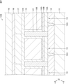
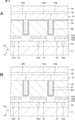
- FIG. 1 is a cross-sectional view showing a schematic configuration of an embodiment of a display device according to a first embodiment.
- FIG. 2A is a cross-sectional view showing a state of the cross section taken along line AA of FIG.
- FIG. 2B is a cross-sectional view showing a state of the cross section taken along the line BB of FIG.
- FIG. 2C is a cross-sectional view showing a state of the cross section taken along the line CC of FIG.
- FIG. 2D is a cross-sectional view showing a state of the cross section taken along the line DD of FIG.
- FIG. 2E is a cross-sectional view showing a state of the cross section taken along line EE of FIG.
- FIG. 2A is a cross-sectional view showing a state of the cross section taken along line AA of FIG.
- FIG. 2B is a cross-sectional view showing a state of the cross section taken along the line BB of FIG.
- FIG. 2C is a
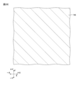
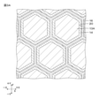
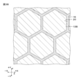
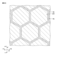
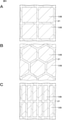
- FIG. 3A is a cross-sectional view corresponding to the state of the AA line cross section of FIG. 1 in one of the modified examples of the display device according to the first embodiment.
- FIG. 3B is a cross-sectional view corresponding to the state of the BB line cross section of FIG. 1 in one of the modified examples of the display device according to the first embodiment.
- FIG. 3C is a cross-sectional view corresponding to the state of the CC line cross section of FIG. 1 in one of the modified examples of the display device according to the first embodiment.
- FIG. 3D is a cross-sectional view corresponding to the state of the DD line cross section of FIG.
- FIG. 3E is a cross-sectional view corresponding to the state of the EE line cross section of FIG.
- FIG. 4A is a cross-sectional view showing a schematic configuration of an embodiment of the display device according to the second embodiment.
- FIG. 4B is a cross-sectional view showing a state of the IVB-IVB line cross section of FIG. 4A.
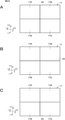
- FIG. 5A is a diagram showing a state of the VV line cross section of FIG. 4A and for explaining an embodiment of the layout of sub-pixels.
- 5B and 5C are diagrams for explaining other layout examples of sub-pixels.
- FIG. 6A is a cross-sectional view showing a schematic configuration of a modified example of the display device according to the second embodiment.
- FIG. 6B is a cross-sectional view showing a schematic configuration of a modified example of the display device according to the second embodiment.
- FIG. 7 is a cross-sectional view showing a schematic configuration of a modified example of the display device according to the second embodiment.
- 8A and 8B are plan views for explaining a modification of the display device according to the second embodiment.
- 9A, 9B, 9C, and 9D are diagrams for explaining the manufacturing method of the display device according to the second embodiment.
- 10A, 10B, 10C, and 10D are diagrams for explaining a method of manufacturing a display device according to a second embodiment.
- FIG. 11 is a cross-sectional view showing a schematic configuration of an embodiment of the display device according to the third embodiment.
- FIGS. 12A, 12B, 12C, and 12D are diagrams for explaining a method of manufacturing a display device according to a third embodiment.
- 13A and 13B are cross-sectional views showing a schematic configuration of a modified example of the display device according to the third embodiment.
- 14A and 14B are cross-sectional views showing a schematic configuration of a modified example of the display device according to the third embodiment.
- 15A, 15B, 15C, and 15D are diagrams for explaining a manufacturing method of a modified example of the display device according to the third embodiment.
- 16A and 16B are cross-sectional views showing a schematic configuration of a modified example of the display device according to the third embodiment.
- FIG. 17A is a cross-sectional view showing a schematic configuration of an embodiment of the display device according to the fourth embodiment.
- FIG. 17B is a plan view showing a schematic configuration of an embodiment of the display device according to the fourth embodiment.
- 18A and 18B are cross-sectional views showing a schematic configuration of an embodiment of a display device according to a fourth embodiment.
- 19A and 19B are cross-sectional views showing a schematic configuration of a modified example of the display device according to the fourth embodiment.
- FIG. 20 is a cross-sectional view showing a schematic configuration of a modified example of the display device according to the fourth embodiment.
- 21A and 21B are cross-sectional views showing a schematic configuration of a modified example of the display device according to the fourth embodiment.
- 22A, 22B, and 22C are diagrams for explaining a modification of the display device according to the fourth embodiment.
- 23A, 23B, and 23C are diagrams for explaining a method of manufacturing a display device according to a fourth embodiment.
- 24A and 24B are diagrams for explaining the manufacturing method of the display device according to the fourth embodiment.
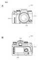
- 25A and 25B are diagrams for explaining an embodiment of an electronic device using a display device.
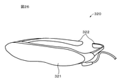
- FIG. 26 is a diagram for explaining an embodiment of an electronic device using a display device.
- FIG. 27 is a diagram for explaining an embodiment of an electronic device using a display device.
- the Z-axis direction is the vertical direction (upper side is + Z direction, the lower side is -Z direction), and the X-axis direction is the front-back direction (front side is + X direction, rear side is -X direction).
- the Y-axis direction is the left-right direction (the right side is the + Y direction and the left side is the ⁇ Y direction), and the description will be made based on this.
- This also applies to FIGS. 3A to 3E and FIGS. 4 to 24.
- the relative magnitude ratio of the size and thickness of each layer shown in each figure such as FIG. 1 is described for convenience, and does not limit the actual magnitude ratio. The rules regarding these directions and the magnitude ratio are the same for each of the figures from FIGS. 3 to 24.
- the display device according to the first embodiment of the present disclosure will be described below by exemplifying a case where the display device is an organic EL (Electroluminescence) display device.
- FIG. 1 is a cross-sectional view showing a configuration example of an organic EL display device (hereinafter, simply referred to as “display device 10A”) according to the first to fourth embodiments of the present disclosure.
- the display device 10A includes a substrate 11, an insulating layer 12, a plurality of light emitting elements 13, an insulating layer 14, a protective layer 15, a protective layer 16, a color filter 17, a filled resin layer 18, and a facing substrate 19. And prepare.
- the display device 10A is a top emission type display device.
- the substrate 11 constitutes the back surface side of the display device 10A
- the facing substrate 19 constitutes the display surface side of the display device 10A.
- the facing substrate 19 side is the top side
- the substrate 11 side is the bottom side.
- the surface on the display surface side of the display device 10A is referred to as a first surface
- the surface on the back surface side of the display device 10A is referred to as a second surface.
- the surface facing the + Z direction is referred to as a first surface
- the surface facing the ⁇ Z direction is referred to as a second surface.
- the display device 10A may be a micro display.
- the display device 10A may be used in various electronic devices. Examples of the electronic device in which the display device 10A is used include a display device for VR (Virtual Reality), MR (Mixed Reality) or AR (Augmented Reality), an electronic viewfinder (EVF) or a small projector. And so on. This also applies to the display devices 10B to 10D, which will be described later.
- the substrate 11 is a so-called backplane and drives a plurality of light emitting elements 13.
- a drive circuit including a sampling transistor for controlling the drive of the plurality of light emitting elements 13 and a drive transistor, and a power supply circuit for supplying power to the plurality of light emitting elements 13 (all shown in the figure). Is provided.
- the substrate 11 may be made of, for example, glass or resin having low permeability of water and oxygen, or may be made of a semiconductor such as a transistor which can be easily formed.
- the substrate 11 may be a glass substrate, a semiconductor substrate, a resin substrate, or the like.
- the glass substrate includes, for example, high strain point glass, soda glass, borosilicate glass, forsterite, lead glass, quartz glass and the like.
- the semiconductor substrate includes, for example, amorphous silicon, polycrystalline silicon, single crystal silicon, and the like.
- the resin substrate contains, for example, at least one selected from the group consisting of polymethylmethacrylate, polyvinyl alcohol, polyvinylphenol, polyether sulfone, polyimide, polycarbonate, polyethylene terephthalate, polyethylene naphthalate and the like.
- the insulating layer 12 is provided on the first surface of the substrate 11 and covers the drive circuit, the power supply circuit, and the like.
- the insulating layer 12 includes a plurality of contact plugs 12A and a plurality of wirings (not shown).
- the contact plug 12A connects the lower electrode 13A constituting the light emitting element 13 and the drive circuit.
- a plurality of wirings are arranged adjacent to each other in the in-plane direction (XY plane direction) of the substrate 11, and each wiring is electrically connected to the lower electrode 13A and the light emitting element 13 by a contact plug 12A or the like. Ru.
- the insulating layer 12 is made of, for example, an organic material or an inorganic material.
- the organic material contains, for example, at least one of polyimide and acrylic resin.
- the inorganic material includes, for example, at least one of silicon oxide, silicon nitride, silicon nitriding and aluminum oxide.
- the plurality of light emitting elements 13 are provided on the first surface side of the substrate 11.
- the plurality of light emitting elements 13 are two-dimensionally arranged in a predetermined arrangement pattern such as a matrix.
- the light emitting element 13 is configured to be capable of emitting white light.
- the light emitting element 13 is, for example, a white OLED or a white Micro-OLED (MOLED).
- MOLED white Micro-OLED
- as the colorization method in the display device 10A a method using a light emitting element 13 and a color filter 17 is used.
- the colorization method is not limited to this, and an RGB coloring method or the like may be used.
- a monochromatic filter may be used instead of the color filter 17, a monochromatic filter may be used.
- the colorization method is the same for the display devices 10B to the display devices 10D, which will be described later.
- the light emitting element 13 includes a lower electrode 13A, an organic layer 13B, and an upper electrode 13C.
- the lower electrode 13A, the organic layer 13B, and the upper electrode 13C are laminated in this order from the substrate 11 side toward the facing substrate 19.
- the lower electrode 13A is provided on the first surface of the insulating layer 12. As shown in FIG. 2A, the lower electrode 13A is electrically separated for each sub-pixel.
- the lower electrode 13A is an anode.
- the lower electrode 13A also functions as a reflective layer, and it is preferable that the lower electrode 13A is made of a material having as high a reflectance as possible and a large work function in order to increase the luminous efficiency.
- the sub-pixel indicates the smallest display division unit composed of one kind of color obtained by further dividing the pixel that is the division unit constituting the screen. For example, one pixel is composed of a combination of adjacent red sub-pixels, green sub-pixels, and blue sub-pixels.
- the lower electrode 13A is composed of at least one of a metal layer and a metal oxide layer. More specifically, the lower electrode 13A is composed of a single-layer film of a metal layer or a metal oxide layer, or a laminated film of a metal layer and a metal oxide layer.
- the metal oxide layer may be provided on the organic layer 13B side or the metal layer may be provided on the organic layer 13B side, but it has a high work function. From the viewpoint of adjoining the layer having the above to the organic layer 13B, it is preferable that the metal oxide layer is provided on the organic layer 13B side.
- the metal layer is, for example, chromium (Cr), gold (Au), platinum (Pt), nickel (Ni), copper (Cu), molybdenum (Mo), titanium (Ti), tantalum (Ta), aluminum (Al). , Magnesium (Mg), Tantalum (Fe), Tungsten (W) and Silver (Ag).
- the metal layer may contain at least one of the above metal elements as a constituent element of the alloy.
- alloys include aluminum alloys and silver alloys.
- Specific examples of the aluminum alloy include, for example, AlNd or AlCu.
- the metal oxide layer contains, for example, at least one of a mixture of indium oxide and tin oxide (ITO), a mixture of indium oxide and zinc oxide (IZO), and titanium oxide (TIO).
- ITO indium oxide and tin oxide
- IZO indium oxide and zinc oxide
- TIO titanium oxide
- the upper electrode 13C is provided so as to face the lower electrode 13A.
- the upper electrode 13C is formed directly above each organic layer 13B described later, and the adjacent upper electrodes 13C are formed in a state of being spatially separated for each sub-pixel, and are formed at electrode connection portions (not shown). It is electrically connected.
- the electrode connection portion may be integrated with or separate from the upper electrode 13C.
- the upper electrode 13C is a cathode.
- the upper electrode 13C is a transparent electrode having transparency to the light generated in the organic layer 13B. Here, it is assumed that the transparent electrode also includes a translucent reflective layer. It is preferable that the upper electrode 13C is made of a material having as high a transparency as possible and a small work function in order to improve the utilization efficiency of the light generated by the light emitting element 13.
- the upper electrode 13C is composed of at least one of a metal layer and a metal oxide layer. More specifically, the upper electrode 13C is composed of a single-layer film of a metal layer or a metal oxide layer, or a laminated film of a metal layer and a metal oxide layer.
- the metal layer may be provided on the organic layer 13B side or the metal oxide layer may be provided on the organic layer 13B side, but it has a low work function. From the viewpoint of making the layer adjacent to the organic layer 13B, it is preferable that the metal layer is provided on the organic layer 13B side.
- the metal layer contains, for example, at least one metal element selected from the group consisting of magnesium (Mg), aluminum (Al), silver (Ag), calcium (Ca) and sodium (Na).
- the metal layer may contain at least one of the above metal elements as a constituent element of the alloy. Specific examples of the alloy include MgAg alloy, MgAl alloy, AlLi alloy and the like.
- the metal oxide contains, for example, at least one of a mixture of indium oxide and tin oxide (ITO), a mixture of indium oxide and zinc oxide (IZO) and zinc oxide (ZnO).
- Organic layer 13B The organic layer 13B is provided between the lower electrode 13A and the upper electrode 13C.
- the organic layer 13B is patterned according to the arrangement of the sub-pixels. As shown in FIG. 2B, the organic layer 13B is formed in a state of being separated for each sub-pixel.
- the organic layer 13B is configured to be capable of emitting white light.
- the organic layer 13B has a structure in which a hole injection layer, a hole transport layer, a light emitting layer, and an electron transport layer are laminated in this order from the lower electrode 13A toward the upper electrode 13C.
- the structure of the organic layer 13B is not limited to this, and layers other than the light emitting layer are provided as needed.
- the hole injection layer is a buffer layer for increasing the hole injection efficiency into the light emitting layer and for suppressing leakage.
- the hole transport layer is for increasing the hole transport efficiency to the light emitting layer. In the light emitting layer, when an electric field is applied, recombination of electrons and holes occurs, and light is generated.
- the light emitting layer is an organic light emitting layer containing an organic light emitting material.
- the electron transport layer is for increasing the electron transport efficiency to the light emitting layer.
- An electron injection layer may be provided between the electron transport layer and the upper electrode 13C. This electron injection layer is for increasing the electron injection efficiency.
- the insulating layer 14 is provided on the first surface of the insulating layer 12.
- the insulating layer 14 electrically separates each lower electrode 13A for each light emitting element 13 (that is, for each sub-pixel).
- the insulating layer 14 has a plurality of openings 14A, and the first surface (the surface facing the upper electrode 13C) of the separated lower electrode 13A is exposed from the openings 14A.
- the insulating layer 14 may cover the separated lower electrode 13A from the peripheral edge portion to the side surface (end surface) of the first surface.
- the peripheral edge portion of the first surface means a region having a predetermined width from the peripheral edge of the first surface toward the inside.
- the protective layer 15 is an upper surface protective layer that protects the main surface (+ Z side surface) on the upper surface side of the light emitting element 13.
- the protective layer 15 is provided on the first surface of the upper electrode 13C, and covers the light emitting element 13 by covering the upper electrode 13C.
- the protective layer 15 suppresses contact between the light emitting element 13 from the upper surface side of the light emitting element 13 and the outside air, and suppresses the infiltration of moisture from the external environment into the light emitting element 13.
- the protective layer 15 may have a function of suppressing oxidation of the metal layer.
- the protective layer 15 is made of, for example, an inorganic material.
- the inorganic material constituting the protective layer 15 a material having low hygroscopicity is preferable.
- the inorganic material constituting the protective layer 15 is selected from the group consisting of silicon oxide (SiO), silicon nitride (SiN), silicon oxide nitride (SiNO), titanium oxide (TIO) and aluminum oxide (AlO). It is preferable to contain at least one of these.
- the protective layer 15 may have a single-layer structure, but may have a multi-layer structure when the thickness is increased. This is to relieve the internal stress in the protective layer 15.
- the protective layer 16 has a second protective portion 16B composed of a first protective portion 16A and a portion excluding the first protective portion 16A located directly above the protective layer 15, and the first protective portion 16A and the second protective layer 16A.
- the protective portion 16B is made of the same material and is continuously and integrally formed.
- the first protective portion covers the surface of the protective layer 15 which is the upper surface protective layer, brings about smoothing of the surface (the surface on the + Z side) together with the second protective portion 16B, and suppresses deterioration of the light emitting element 13.
- the second protective portion 16B is formed between the adjacent first protective portions 16A, and is formed so as to enter between the adjacent protective layer 15 and the adjacent light emitting elements 13.
- the second protective portion 16B also penetrates into the insulating layer 12.
- the second protective portion 16B is an inter-element separation wall that covers the side end surface 130 of the light emitting element 13.
- the element-to-element separation wall is a wall extending in a direction different from the direction of riding on the first surface of any of the layers (lower electrode 13A, organic layer 13B, upper electrode 13C) of the light emitting element 13. It is a structural part.
- the second protective portion 16B can suppress deterioration of the light emitting element 13 due to the outside air by covering the side end surface 130 of the light emitting element 13.
- the second protective portion 16B is directed from the light emitting element 13 toward the protective layer 15 (+ Z) along the thickness direction (Z-axis direction) of the light emitting element 13 with reference to the position facing the side end surface 130 of the light emitting element 13. Extends in the direction). Then, in the example of FIG. 1, the upper end (extending end) of the second protection portion 16B coincides with the upper surface side of the first protection portion 16A, and the surface of the first protection portion 16A and the upper end surface of the second protection portion 16B are aligned with each other. It is flush. As shown in the example of FIG. 1, the lower end of the second protection portion 16B is located further below the lower electrode 13A of the light emitting element 13, which will be described later in the position further below the light emitting element 13. It is preferable from the viewpoint that a low refractive index portion (void portion 20 in the example of FIG. 1) can be formed.
- the material forming the protective layer 16 (the material forming the first protective portion 16A and the second protective portion 16B) has a refractive index in the state of the protective layer 16 higher than that of the protective layer 15 forming the upper surface protective layer. It is preferable that the value of the refractive index is low. Further, since the refractive index of the protective layer 16 is smaller than the refractive index of the protective layer 15, it is possible to more effectively prevent the light generated by the light emitting element from leaking to the adjacent sub-pixel side. Therefore, when the material forming the protective layer 16 satisfies the refractive index as described above, it is possible to more effectively prevent the light generated by the light emitting element from leaking to the adjacent sub-pixel side.
- the material forming the protective layer 16 is preferably made of a material having a step coverage value of less than 1. Further, the material forming the protective layer 16 is preferably made of a material having a lower moisture permeability than the protective layer 15 serving as the upper surface protective layer. By forming the protective layer 16 with such a material, the void portion 20 can be formed more efficiently.
- Examples of the material for forming the protective layer 16 include SiN, Al 2 O 3 , TiO 2 and the like formed by a method such as a PECVD (plasma-enhanced chemical vapor deposition) method or a sputtering method.
- PECVD plasma-enhanced chemical vapor deposition
- a low refractive index portion having a lower refractive index than that of the second protective portion 16B is formed inside the second protective portion 16B forming the separation wall between the elements.
- the low refractive index portion is formed in a shape extending in the thickness direction (Z-axis direction) of the light emitting element.
- the low refractive index portion is a portion having a refractive index lower than the refractive index of the second protective portion 16B.
- the low refractive index portion include a gas space portion filled with a specific gas such as nitrogen, a liquid portion filled with a specific liquid, and the like. As the gas space portion, an air-filled void portion can be exemplified.
- the refractive index of the low refractive index portion and the refractive index of the second protected portion are the refractive index of the low refractive index portion and the refractive index of the second protected portion in the display device.
- the refractive index of the void portion 20 is smaller than that of the second protective portion 16B, total reflection of light may occur at the interface between the portion made of the material forming the protective layer 16 and the void portion 20. It will be easy.
- the void portion 20 is formed as a low refractive index portion.
- the description will be continued by taking the case where the void portion 20 is formed as a low refractive index portion as an example.
- the length and position of the gap 20 in the vertical direction are not limited.
- the gap 20 may be formed at at least one of the lower electrode 13A, the organic layer 13B, the upper electrode 13C, and the protective layer 15, and has a length corresponding to the position. good.
- the gap portion 20 exists at any of the positions of the lower electrode 13A, the organic layer 13B, the upper electrode 13C, and the protective layer 15 in the vertical direction (Z-axis direction). Further, it exists up to a height position near the center of the first protection portion 16A in the Z-axis direction.
- the example of the void portion 20 is not limited to this, and may be formed, for example, at the position of the organic layer 13B with a length corresponding to the thickness of the organic layer 13B.
- the upper end of the gap portion 20 is above the interface between the light emitting element 13 and the protective layer 15 (+ Z direction side). It is preferable to have.
- the gap portion 20 is formed from the position near the first surface of the substrate 11 to the position near the second surface of the color filter 17, so that the light generated in the organic layer 13B is surely leaked to the adjacent sub-pixel side. It is even more preferable from the viewpoint that it can be made difficult.
- the lower end of the gap 20 may be located below the lower electrode 13A as well as the lower end of the second protective portion 16B. It is more preferable that the position in the insulating layer 12 is lower than the position between adjacent wirings or the position between adjacent wirings. In this case, since the gap portion 20 is arranged between the wirings adjacent to each other in the XY plane direction, the capacitance (parasitic capacitance) of the capacitor formed by the adjacent wirings is compared with the case where the gap portion 20 does not exist. ) Can be reduced.
- the cross-sectional shape of the gap portion 20 has a bottom surface portion 20A, a bottom surface portion 20A thereof, and a side wall portion 20B.
- the gap portion 20 preferably has a taper angle (angle ⁇ in FIG. 1) formed by the bottom surface portion 20A and the side wall portion 20B of 90 ° or less.
- the taper angle ⁇ is formed in a forward taper shape of 30 ° or less.
- this does not prohibit the shape of the gap 20 from being reverse-tapered, and the shape of the gap 20 may be reverse-tapered.
- the cross-sectional shape of the gap portion 20 is a cross-sectional trapezoidal shape in the example of FIG. 1, but the cross-sectional shape is not limited to this, and may be a triangle, a polygon of a quadrangle or more, or a curved surface portion.
- the void portion 20 is formed only between the adjacent protective layers 15. You may. In that case, the second protective portion 16B in the protective layer 16 may be formed only in the portion between the adjacent protective layers 15, or both between the adjacent protective layers 15 and between the adjacent light emitting elements 13. It may be formed over a portion of. When the second protective portion 16B is formed only in the portion between the adjacent protective layers 15, the organic layer 13B and the upper electrode 13C are not separated for each sub-pixel but are shared among the sub-pixels.
- the color filter 17 is provided on the protective layer 16.
- the color filter 17 is, for example, an on-chip color filter (OCCF).
- the color filter 17 includes, for example, a red filter, a green filter, and a blue filter.
- the red filter, the green filter, and the blue filter are provided facing the light emitting element 13 for the red sub-pixel, the light emitting element 13 for the green sub pixel, and the light emitting element 13 for the blue sub pixel, respectively.
- the white light emitted from each of the light emitting elements 13 in the red sub-pixel, the green sub-pixel, and the blue sub-pixel passes through the above-mentioned red filter, green filter, and blue filter, respectively, so that the red light and the green light are emitted.
- Blue light is emitted from the display surface, respectively.
- a light-shielding layer (not shown) may be provided between the color filters of each color, that is, between the sub-pixels.
- the color filter 17 is not limited to the on-chip color filter, and may be provided on one main surface of the facing substrate 19.
- the filling resin layer 18 is provided between the color filter 17 and the facing substrate 19.
- the filled resin layer 18 has a function as an adhesive layer for adhering the color filter 17 and the facing substrate 19.
- the packed resin layer 18 contains, for example, at least one of a thermosetting resin and an ultraviolet curable resin.
- the facing substrate 19 is provided so as to face the substrate 11. More specifically, the facing substrate 19 is provided so that the second surface of the facing substrate 19 and the first surface of the substrate 11 face each other.
- the facing substrate 19 and the filled resin layer 18 seal the light emitting element 13, the color filter 17, and the like.
- the facing substrate 19 is made of a material such as glass that is transparent to each color light emitted from the color filter 17.
- a drive circuit, a power supply circuit, and the like are formed on the first surface of the substrate 11 by using, for example, a thin film forming technique, a photolithography technique, and an etching technique.
- an insulating layer 12 is formed on the first surface of the substrate 11 so as to cover the drive circuit and the power supply circuit, and then a plurality of contact plugs 12A are formed on the insulating layer 12.
- a laminated film of a metal layer and a metal oxide layer is formed on the first surface of the substrate 11 by a sputtering method, and then the laminated film is patterned by using, for example, a photolithography technique and an etching technique.
- the lower electrode 13A separated for each light emitting element 13 (that is, for each sub pixel) is formed.
- an insulating layer 14 is formed on the first surface of the insulating layer 12 so as to cover the plurality of lower electrodes 13A, and then the insulating layer 14 is patterned using a photolithography technique and an etching technique. do. As a result, a plurality of openings 14A are formed in the insulating layer 14. If the lower electrode 13A is not easily damaged by the groove forming process (groove processing) described later, the insulating layer 14 may be omitted.
- the hole injection layer, the hole transport layer, the light emitting layer, and the electron transport layer are laminated on the first surface of the first surface of the lower electrode 13A in this order to form an organic layer.
- the upper electrode 13C is formed on the first surface of the organic layer 13B by, for example, a vapor deposition method or a sputtering method. As a result, a plurality of light emitting elements 13 are formed on the first surface of the insulating layer 12.
- the protective layer 15 is formed on the first surface of the upper electrode 13C by, for example, a CVD method or a vapor deposition method. Then, the light emitting element and the protective layer are grooved along the layout of the sub-pixels by, for example, photolithography technology and etching technology. In the display device of FIG. 1, a groove is formed to the inside of the insulating layer 12. Further, the protective layer 16 is formed on the surface of the protective layer 15 and inside the groove by a method such as a PECVD method or a sputtering method.
- the gap portion 20 is formed in the second protection portion 16B. Will be done.
- the color filter 17 is formed on the first surface of the protective layer 15 by, for example, photolithography.
- the color filter 17 is covered with the filled resin layer 18, and then the facing substrate 19 is placed on the filled resin layer 18.
- the display device 10A is sealed.
- the display device 10A shown in FIG. 1 is obtained.
- a second protective portion 16B serving as an inter-element separation wall is formed between adjacent sub-pixels so as to face the side end surface 130 of the light emitting element 13.
- a low refractive index portion is formed inside the second protective portion 16B.
- the low refractive index portion is the gap portion 20, and the gap portion 20 is located below the lower electrode 13A, and the wiring is adjacent to the insulating layer 12.
- the capacitance between wirings can be reduced.
- the shape of the sub-pixel is rectangular, but the shape is not limited to this, and may be formed into a hexagonal shape as shown in FIGS. 3A to 3E. Further, the arrangement of the sub-pixels is not limited to the matrix shape, and may be a honeycomb shape as shown in FIGS. 3A to 3E. Even in such a case, it becomes possible to suppress the leakage of light to the adjacent sub-pixels in the same manner as described in the above-mentioned action and effect.
- FIG. 4A is a cross-sectional view showing a configuration example of an organic EL display device (display device 10B) according to an example of the second embodiment.
- FIG. 4B is a diagram illustrating a state of the IVB-IVB line cross section of FIG. 4A.
- the display device 10B is a top emission type display device.
- the display device 10B includes a substrate 11, an insulating layer 12, a plurality of light emitting elements 13, a protective layer 15 as an upper surface protective layer, a separation film 21 as a separation wall between elements, a color filter 17, and a filled resin layer. 18 and a facing substrate 19 are provided.
- the substrate 11, the insulating layer 12, the protective layer 15, the color filter 17, the filled resin layer 18, and the facing substrate 19 are the same as those in the first embodiment.
- the display device 10B of the second embodiment it is not necessary to provide the structure of the insulating layer 14 in the first embodiment.
- the plurality of light emitting elements 13 are provided on the first surface of the substrate 11, include a lower electrode 13A and an organic layer 13B, and an upper electrode laminated on the organic layer 13B.
- First upper electrode 13D is provided.
- the lower electrode 13A and the organic layer 13B are the same as those in the first embodiment, and are separated from each other for each sub-pixel.
- the upper electrode laminated on the organic layer 13B is the first upper electrode 13D, which is separated from each other for each sub-pixel.
- the first upper electrode 13D faces the lower electrode 13A, and the first upper electrode 13D faces the protective layer 15.
- the second upper electrode 13E electrically connects the adjacent first upper electrodes 13D to each other.
- the second upper electrode 13E extends along the surface of the separation membrane 21 to the extending end 21A of the separation membrane 21 with the facing position of the first upper electrode 13D and the separation membrane 21 as the base end.
- the position of the upper end portion of the second upper electrode 13E and the position of the surface of the protective layer 15 are aligned with the second upper electrode 13E formed on the surface of the separation film 21.
- the second upper electrode 13E is formed so as to cover the entire portion of the separation membrane 21 extending upward from the first upper electrode 13D.
- the second upper electrode 13E is further made of a reflective material as described later, the light traveling diagonally among the light generated by the light emitting element 13 is effectively reflected by the second upper electrode 13E. It is possible to increase the efficiency of light utilization.
- the second upper electrodes 13E are formed in a grid pattern according to the layout of the sub-pixels, and the individual first upper electrodes 13D are formed in a rectangular shape and arranged in a matrix.
- the first upper electrode 13D and the second upper electrode 13E are cathodes.
- the first upper electrode 13D is a transparent electrode having transparency to the light generated in the organic layer 13B.
- the transparent electrode also includes a translucent reflective layer.
- the first upper electrode 13D is made of a material having as high a transparency as possible and a small work function in order to increase the luminous efficiency.
- the reflectance of the second upper electrode 13E is larger than the reflectance of the first upper electrode 13D.
- the reflectance of the second upper electrode 13E and the reflectance of the first upper electrode 13D are the reflectance of the second upper electrode 13E and the reflectance of the first upper electrode 13D in the state of the display device 10B.
- a reflective material can be used as the material of the second upper electrode 13E. Examples of the reflective material include silver (Ag), aluminum (Al), and tungsten (W).
- the display device 10B is formed with a separation film 21 that covers the side end surface 130 side of the light emitting element 13 as an inter-element separation wall.
- the separation film 21 is arranged between adjacent light emitting elements 13, and separates the lower electrode 13A, the organic layer 13B, and the first upper electrode 13D forming the light emitting element 13 for each sub-pixel.
- the upper end side portion of the separation film 21 extends from the light emitting element 13 toward the protective layer 15 along the thickness direction (Z-axis direction) of the light emitting element 13.
- the separation film 21 has a shape that extends from the light emitting element 13 toward the protective layer 15 (Z-axis direction) instead of the surface direction (XY plane direction) of the light emitting element 13. It becomes difficult to cover the light emitting region of the light emitting element, and a wider light emitting region can be secured.
- the separation membrane 21 is made of an insulator.
- the separation film 21 include an inorganic insulating film and an organic insulating film.
- the inorganic insulating film include SiO 2 , SiN, and SiON.
- the organic insulating film include polyimide and the like.
- the length of the separation membrane 21 in the vertical direction (Z-axis direction) is larger than the sum of the thickness of the lower electrode 13A, the thickness of the organic layer 13B, and the thickness of the first upper electrode 13D. It is preferable from the viewpoint of facilitating the formation of a portion extending above the electrode 13D.
- the lower end of the separation membrane 21 is located near the insulating layer 12 below the lower end of the lower electrode 13A, and the separation membrane 21 separates the lower electrode 13A for each sub-pixel.
- the separation membrane 21 may be located at the lower end of the lower electrode 13A.
- the separation membrane 21 may separate the lower electrode 13A for each sub-pixel.
- the upper end of the separation film 21 is located slightly below the position of the surface of the protective layer 15, and the second upper electrode 13E is formed on the surface of the separation film 21.
- the position of the extending end portion of the protective layer 15 and the position of the surface of the protective layer 15 are aligned.
- the refractive index of the separation membrane 21 is smaller than the refractive index of the second upper electrode 13E. In this case, among the light generated by the light emitting element 13, the light traveling diagonally can be totally reflected at the interface between the second upper electrode 13E and the separation film 21, and the light utilization efficiency can be improved.
- the refractive index of the separation membrane 21 and the refractive index of the second upper electrode 13E are the refractive index of the separation membrane 21 and the refractive index of the second upper electrode 13E in the state of the display device 10B.
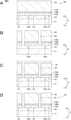
- FIGS. 9A to 9D and FIGS. 10A to 10D are diagrams for explaining the manufacturing method of the display device 10B according to the second embodiment.
- the step of forming the first laminated body in which the lower electrode 13A, the organic layer 13B, the first upper electrode 13D, and the protective layer 15 are laminated in this order on the substrate 11 on which the insulating layer 12 is formed is carried out as shown below. ..
- a drive circuit, a power supply circuit, and the like are formed on the first surface of the substrate 11 by using a thin film forming technique, a photolithography technique, and an etching technique.
- a CVD method an insulating layer 12 is formed on the first surface of the substrate 11 so as to cover the drive circuit and the power supply circuit, and then a plurality of contact plugs 12A are formed on the insulating layer 12.
- a laminated film (lower electrode) of a metal layer and a metal oxide layer is formed on the first surface of the substrate 11 by a sputtering method.
- the hole injection layer, the hole transport layer, the light emitting layer, and the electron transport layer are laminated on the first surface of the first surface of the lower electrode 13A in this order to form an organic layer.
- the first upper electrode 13D is formed on the first surface of the organic layer 13B by a vapor deposition method or a sputtering method.
- the protective layer 15 is formed on the first surface of the first upper electrode 13D by a CVD method or a vapor deposition method.
- the first laminated body 40 is formed.
- a step of forming a first groove from the protective layer 15 to a predetermined depth in the first laminated body 40 at a predetermined position according to the layout of the sub-pixels (first step). Grooving process) is performed.
- the first grooving step is a step of grooving the light emitting element 13 and the protective layer 15 along the layout of the sub-pixels by, for example, a photolithography technique and an etching technique.
- the protective layer 15, the first upper electrode 13D, the organic layer 13B, the lower electrode 13A, and the insulating layer 12 are collectively grooved to form the first groove 22.
- a step of forming the separation film 21 in the first groove 22 is carried out by, for example, a CVD (Chemical Vapor Deposition) method, a coating method, or the like.
- the material forming the separation film 21 is also laminated on the outside of the first groove 22, such as on the surface of the protective layer 15, so that the outer laminated portion of the first groove 22 is as shown in FIG. 9C. Is formed, but the outer laminated portion of the first groove 22 is removed by a CMP (chemical mechanical polishing) method, an etch back method, or the like.
- the second laminated body 41 is formed as shown in FIG. 9D.
- the CVD method for example, an inorganic insulating film such as SiO 2 , SiN, or SiON can be formed.
- an organic insulating film such as polyimide can be formed.
- a step (second groove processing step) of forming the second groove 23 from the protective layer 15 to the position of the first upper electrode 13D is carried out in a predetermined region around the separation film 21.
- the second grooving step is a step in which grooving is performed by, for example, a photolithography technique and an etching technique, similarly to the above-mentioned first groove.
- the depth of the second groove 23 is such that it reaches the first upper electrode 13D, and the first upper electrode 13D is exposed on the bottom surface of the second groove 23.
- Reference numeral 50 in FIG. 10A is a resist for forming the second groove 23.
- a step of forming the second upper electrode 13E in the second groove 23 is carried out.
- the material forming the second upper electrode is also laminated on the outside of the second groove, such as on the surface of the protective film, so that the outer laminated portion of the second groove 23 is laminated as shown in FIG. 10C.
- the outer laminated portion of the second groove is removed by a CMP method, an etchback method, or the like, as in the case of the outer laminated portion of the first groove.
- the third laminated body 42 is formed.
- the outer laminated portion of the second groove 23 is left unremoved in the case of the third modification described later in the second embodiment.
- the color filter 17 is formed on the first surface of the third laminated body 42 by, for example, photolithography.
- the color filter 17 is covered with the filled resin layer 18, and then the facing substrate 19 is placed on the filled resin layer 18.
- the display device 10B is sealed. From the above, the display device 10B is obtained.
- the lower electrode 13A, the organic layer 13B, and the first upper electrode 13D forming the light emitting element 13 by the separation film 21 are separated for each sub-pixel.
- the organic layer 13B is surrounded by the separation film 21 and separated for each sub-pixel, it is possible to suppress the leakage of light in the lateral direction to the adjacent sub-pixels.
- the separation film 21 extends in the vertical direction, an insulating film is formed so as to ride on the peripheral edge of the first electrode patterned and formed for each sub-pixel, and the separation film 21 is separated for each sub-pixel. Therefore, it becomes easier to secure a wider light emitting region of the light emitting element.
- the second upper electrode 13E has a higher reflectance than the first upper electrode 13D, so that the light generated by the light emitting element 13 is reflected by the second upper electrode 13E. This makes it possible to prevent the light generated by the light emitting element 13 from leaking to the adjacent sub-pixel side.
- the separation membrane 21 has a lower refractive index than the second upper electrode 13E, so that the light generated by the light emitting element 13 is the second upper electrode 13E and the separation membrane 21. It becomes easy to totally reflect at the interface of the above, and it becomes possible to suppress the light generated by the light emitting element 13 from leaking to the adjacent sub-pixel side (suppress the light leakage between the adjacent pixels).
- the light generated by the light emitting element 13 is suppressed from leaking to the adjacent sub-pixels, so that the color mixing can be suppressed and the viewing angle can be suppressed. Deterioration can be suppressed.
- the shape of the sub-pixels is formed in a rectangular shape as shown in FIGS. 4B and 5A, and a plurality of sub-pixels are arranged separately from each other in a matrix.
- the shape of the sub-pixels is not limited to this, and may be a hexagonal shape or a striped shape as shown in FIGS. 5B and 5C.
- the arrangement of the sub-pixels is not limited to the matrix shape, and may be a honeycomb shape as shown in FIG. 5B. Even in such a case, unintended light emission due to current leakage is suppressed, as described in the above-mentioned action and effect. In addition, it becomes possible to suppress light leakage to adjacent sub-pixels.
- Modification 2 Regarding the display device 10B according to the second embodiment, in the above description, the position of the extended end portion of the second upper electrode 13E and the surface of the protective layer 15 in a state where the second upper electrode 13E is formed on the surface of the separation film 21.
- the case where the positions are aligned is taken as an example.
- the display device 10B according to the second embodiment is not limited to this example, and the extending end portion of the second upper electrode 13E is further above (as shown in FIG. 6A) beyond the position of the surface of the protective layer 15. It may be located in the + Z direction) and enter the color filter 17, or may not reach the position of the surface of the protective layer 15 as shown in FIG. 6B.
- the second upper electrode 13E is formed along the surface of the separation film 21 so as to cover the surface of the separation film 21.
- the display device 10B according to the second embodiment is not limited to this example.
- the second upper electrode 13E is not only formed along the surface of the separation membrane 21 up to the extending end of the separation membrane 21, but also protected from the extending end of the separation membrane 21. It may extend along the surface of the layer 15.
- a portion extending along the surface of the protective layer 15 is referred to as a extending electrode portion 24.
- the extending electrode portion 24 preferably covers the entire surface of the protective layer 15.
- the second upper electrode 13E is a transparent electrode or a translucent electrode from the viewpoint of allowing the light generated from the light emitting element 13 to pass through the extending electrode portion 24 and be efficiently taken out to the outside. It is preferable that it is formed.
- the second upper electrode 13E When the second upper electrode 13E is formed of a translucent electrode, the second upper electrode 13E has an extended electrode portion, and the separation distance between the light emitting surface of the organic layer 13B and the extended electrode portion 24 By adjusting the above, it is possible to improve the light extraction effect accompanying the light resonance effect, and it is possible to obtain a display device 10B having excellent brightness.
- the second upper electrode 13E was formed so as to cover the entire surface of the portion of the separation membrane 21 extending upward from the first upper electrode 13D, but the display device 10B according to the second embodiment is this.
- the present invention is not limited to the example, and as shown in FIGS. 8A and 8B, the separation membrane 21 may be formed so as to cover a part of the portion extending upward from the first upper electrode.
- the portion of the separation membrane 21 extending upward from the first upper electrode 13D corresponding to the apex portion of the adjacent sub-pixel. It may be formed to cover.
- the portion of the separation membrane 21 in which the second upper electrode 13E extends upward from the first upper electrode 13D corresponds to the side portion of the adjacent sub-pixel. It may be formed to cover.
- the side wall protective film may be interposed between the side end surface of the organic layer 13B and the separation film 21 (third embodiment).
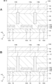
- FIG. 11 is a cross-sectional view showing a configuration example of an organic EL display device (display device 10C) according to an example of the third embodiment.
- the display device 10C has a side wall protective film in addition to each configuration of the display device 10B according to the second embodiment. As shown in the example of FIG. 11, the display device 10C includes a substrate 11, an insulating layer 12, a plurality of light emitting elements 13, a protective layer 15, a side wall protective film 25, and a separation film 21 as an inter-element separation wall. A color filter 17, a filling resin layer 18, and a facing substrate 19 are provided.
- the side wall protective film 25 is interposed between the side end surface of the organic layer 13B and the separation film 21. As shown in FIG. 11, it is preferable that the side wall protective film 25 covers the entire side end surface of the organic layer 13B while being in contact with the side end surface of the organic layer 13B.
- the side wall protective film 25 is an insulating film, and is a processed by-product film containing a by-product (depot) generated by etching processing.
- the side wall protective film 25 assists in forming the separation film 21 while restricting the exposure of the organic layer 13B to the external environment.
- the etching process referred to here refers to the process by the etching method in the first groove processing step shown in the description of the manufacturing method of the display device 10C according to the third embodiment described later.
- the etching process either a dry etching method or a wet etching method can be carried out, but from the viewpoint of more reliably realizing the depot, the etching process is preferably a dry etching method.
- the side wall protective film 25 shown in FIG. 11 is formed so that its thickness is uniform, but this is not limited to the case where the thickness of the side wall protective film 25 is uniform.
- the side wall protective film 25 may be formed so that the thickness gradually decreases as the distance from the vicinity of the auxiliary layer 26 described later increases.
- the auxiliary layer 26 is interposed between the lower electrode 13A and the substrate 11 or between the first upper electrode 13D and the protective layer 15. be.
- the auxiliary layer 26 is formed between the lower electrode 13A and the substrate 11 under the lower electrode 13A.
- the contact plug 12A is also formed in the auxiliary layer 26, and the electrical connection with the drive circuit on the substrate 11 side is secured.
- the auxiliary layer 26 is a depot generation film made of a material that easily causes depot during etching.
- a material for the auxiliary layer 26, which easily forms a by-product (depot) during etching for example, a difficult-to-etch material having a lower volatility of a metal halogen compound and a stronger metal-oxygen bond is used. It is preferably used.
- the material of the auxiliary layer 26 it is preferable to use a transition metal oxide such as Al2O3 . However, this does not mean that the material of the auxiliary layer 26 is limited to the transition metal oxide.
- the material of the auxiliary layer 26 may be any material that can form an insulating film on the side end surface of the organic layer 13B.
- the side wall protective film 25 is formed so as to extend from the auxiliary layer 26 along the side end surface 130 of the light emitting element 13 with the auxiliary layer 26 as the base end.
- the side wall protective film 25 contains at least one element forming the auxiliary layer 26.
- the film composition of the side wall protective film 25 is different from the film composition of the separation film 21.
- the auxiliary layer 26, the lower electrode 13A, the organic layer 13B, the first upper electrode 13D, and the protective layer 15 are laminated in this order on the substrate 11 on which the insulating layer 12 is formed, and the first laminated body 43 is formed.
- a resist 51 is provided in the first laminated body 43, and a first groove 27 is formed in the protective layer 15 at a predetermined position as shown in FIG. 12C.
- each layer forming the light emitting element 13 is etched (groove processing step).
- the first groove 27 is further formed downward, and the auxiliary layer 26 is also etched together with the lower electrode 13A, the organic layer 13B, and the first upper electrode 13D forming the light emitting element 13.
- the auxiliary layer 26 is also etched together with the lower electrode 13A, the organic layer 13B, and the first upper electrode 13D forming the light emitting element 13.
- a depot is generated and adheres to the side end faces of the lower electrode 13A, the organic layer 13B, and the first upper electrode 13D to form the side wall protective film 25 (FIG. 12D). In this way, a state in which the side wall protective film 25 is formed along the inner wall of the first groove 27 is formed.
- the same step as the manufacturing method of the display device according to the second embodiment is carried out. That is, a step of forming the separation film 21 in the first groove 27 and a step of forming a second groove 23 from the protective layer 15 to the position of the first upper electrode 13D in a predetermined region around the separation film 21.
- the step of forming the second upper electrode 13E in the second groove 23 is carried out. After the second upper electrode 13E is formed, the color filter 17, the filled resin layer 18, and the facing substrate 19 are laminated. As a result, the display device 10C according to the third embodiment is obtained.
- the side wall protective film is formed so as to cover the side end faces of the organic layer.
- the side wall protective film is a depot generation film formed at the time of etching processing in the step before forming the separation film (first groove processing step). Therefore, even when the separation membrane is formed after the first grooving step, the side end faces of the organic layer are suppressed from being exposed to an external environment (under a low vacuum environment), and the organic layer is prevented from being exposed. The characteristics of can be improved.
- FIGS. 12A to 12D a display device is shown when the auxiliary layer 26 does not remain inside the first groove 27 during the grooving process. That is, in the display device 10C shown in FIG. 11 obtained in this case, the side wall protective film 25 is not provided on the lower end surface of the separation film 21.
- the display device according to the third embodiment is not limited to this, and as shown in FIG. 14A, the side wall protective film 25 may be provided on the lower end surface of the separation film 21. This can be realized by leaving the auxiliary layer 26 in the first groove 27 during the first groove processing step.
- auxiliary layer 26 is located in a predetermined region between the sub-pixels. It may be formed in a limited manner.
- the auxiliary layer 26 is formed at a position corresponding to the side end surface 130 of the light emitting element 13 when the thickness direction of the light emitting element 13 is the line-of-sight direction, and at a position below the lower electrode 13A.
- the side wall protective film 25 extends upward from the auxiliary layer 26.
- the auxiliary layer 26 may be interposed between the first upper electrode 13D and the protective layer 15.
- Such a display device 10C can be manufactured, for example, as follows.
- the lower electrode 13A, the organic layer 13B, and the first upper electrode 13D are formed on the surface of the substrate 11 in the same manner as in the manufacturing method of the display device according to the second embodiment.
- the auxiliary layer 26 is formed on the first upper electrode 13D (FIG. 15A).
- a resist 52 is provided on the auxiliary layer 26 (FIG. 15B), and a first groove 27 is formed in the auxiliary layer 26 at a predetermined position corresponding to a pixel layout such as a sub pixel by using a photolithography technique and an etching technique. do.
- a depot is attached to the inner wall portion of the first groove 27 (FIG. 15C).
- a groove processing step is carried out by a photolithography technique, an etching technique, or the like.
- the lower electrode 13A, the organic layer 13B, and the first upper electrode 13D forming the light emitting element 13 are etched, and the first groove 27 is further formed downward.
- the depot derived from the auxiliary layer 26 also adheres to the side end surfaces of the lower electrode 13A, the organic layer 13B, and the first upper electrode 13D, and the side wall protective film 25 is formed. It is formed (Fig. 15D). In this way, a state in which the side wall protective film 25 is formed in the first groove 27 is formed.
- the separation film 21 is formed inside the first groove 27 by a method such as a CVD method or a coating method.
- a method such as a CVD method or a coating method.
- the material laminated on the outside of the first groove 27 is removed by the CMP method or the etchback method.
- a protective layer 15 is formed on the surface side of the auxiliary layer 26.
- a step of forming a groove in the protective layer 15 is performed at a position corresponding to the first groove 27 with respect to the protective layer 15.
- the separation film 21 is formed inside the groove formed in the protective layer 15 by a method such as a CVD method or a coating method. As a result, the separation film 21 is formed from the surface position of the protective layer 15 to the position of the lower electrode 13A along the thickness direction of the light emitting element 13. From this point onward, a display device can be obtained in the same manner as in the method for manufacturing a display device according to the second embodiment described above.
- a step of forming the second groove 23 from the protective layer 15 to the position of the first upper electrode 13D in a predetermined region around the separation membrane 21, and a step of forming the second upper electrode 13E in the second groove 23. Is carried out. After the second upper electrode 13E is formed, the color filter 17, the filled resin layer 18, and the facing substrate 19 are laminated. As a result, the display device 10C is obtained.
- the side wall protective film 25 shown in FIG. 14B is formed so that its thickness is uniform, but this is not limited to the case where the thickness of the side wall protective film 25 is uniform.
- the side wall protective film 25 may be formed so that the thickness gradually decreases as the distance from the vicinity of the auxiliary layer 26 described later increases.
- the display device according to the fourth embodiment of the present disclosure will be described below by taking the case where the display device is an organic EL display device as in the first embodiment as an example.
- FIGS. 17A and 17B are cross-sectional views showing a configuration example of an organic EL display device (display device 10D) according to an example of the fourth embodiment.
- the display device 10D is a top emission type display device.
- the display device 10D includes a substrate 11, an insulating layer 12, a plurality of light emitting elements 13, a protective layer 15, a light absorbing layer 28, and a color filter 17.
- the description of the insulating layer corresponding to the insulating layer 14 in the first embodiment is omitted. This also applies to FIGS.
- the insulating layer corresponding to the insulating layer 14 is the same as that of the insulating layer 14 in the first embodiment. It may be omitted.
- the substrate 11, the insulating layer 12, the protective layer 15 as the upper surface protective layer, and the color filter 17 are the same as those in the first embodiment.
- a plurality of color filters 17 are provided according to the type of sub-pixels.
- the display device 10D includes a red filter 17R, a green filter 17G, and a blue filter 17B as the color filter 17. The case will be described.
- the red filter 17R, the green filter 17G, and the blue filter 17B are provided facing the light emitting element 13 for the red sub-pixel, the light emitting element 13 for the green sub pixel, and the light emitting element 13 for the blue sub pixel, respectively, and display.
- the gaps or boundaries of the adjacent color filters 17 are located in the gaps of the adjacent light emitting elements 13.
- the light absorption layer 28 is formed at a position of a gap or a boundary between adjacent color filters 17 in a plan view of the display device 10D (in a plan view of the light emitting element 13).
- FIG. 17B is a diagram illustrating the positional relationship between the color filter 17 and the light absorption layer 28.
- the light absorption layer 28 is formed at a position between the color filter 17 and the lower electrode 13A in the thickness direction of the light emitting element 13.
- the light absorption layer 28 has a shape extending from the color filter 17 toward the substrate 11 (downward), and has a width W (width W) in a direction along the in-plane direction (XY plane direction) of the color filter 17. ),
- the length H in the direction along the depth direction of the color filter 17 is formed to be longer (H> W).
- the lower end of the light absorption layer 28 is located above the light emitting element 13. In this case, it is possible to prevent the incident light L of the external light incident obliquely from propagating across the sub-pixels.
- a black color filter, a complementary color filter, a non-adjacent color filter, an absorption film, or the like can be used.
- a black color filter a color filter using carbon, titanium black or the like as a coloring material can be exemplified.
- the complementary color filter a color filter using a complementary color material for the color of the color filter which is the base end of the light absorption layer 28 can be exemplified.
- the non-adjacent color filter can exemplify a color filter corresponding to a color type other than that color type when the color types of the adjacent color filters serving as the base end of the light absorption layer 28 are different.
- the color filter 17 includes a red filter 17R, a green filter 17G, and a blue filter 17B
- the light absorption layer 28 is located at the boundary between the green filter 17G and the red filter 17R.
- an organic material film, an inorganic material film, or the like can be exemplified.
- a resin film containing a black pigment for example, carbon black
- a metal oxide film, a single metal film, or the like is preferable, and a metal oxide film is particularly preferable from the viewpoint of excellent light absorption.
- [4-2 Manufacturing method of display device] The method for manufacturing the display device according to the fourth embodiment can be carried out, for example, as described below. A case where the display devices shown in FIGS. 17A and 17B are manufactured will be described as an example.
- the insulating layer 12, the lower electrode 13A, the organic layer 13B, and the upper electrode 13C are placed on the first surface of the substrate 11 on which the insulating layer 12 is formed.
- the protective layer 15 is laminated to form the first laminated body 44 (FIG. 23A).
- the insulating layer is also formed.
- the first laminated body 44 is grooved along the layout of the sub-pixels by, for example, a photolithography technique and an etching technique to form a groove 29 having a predetermined depth (FIG. 23B). ..
- the groove 29 is formed at a depth within the protective layer 15 to a predetermined position.
- a step of forming the light absorption layer 28 in the groove 29 is carried out by a method such as a CVD method or a coating method.
- the color filter 17 is formed on the surface side of the protective layer 15 by, for example, photolithography (FIG. 24A). Therefore, the color filter 17 is an on-chip type.
- a lens 30 may be formed on the 17th surface of the color filter (FIG. 24B). The lens 30 can be formed by applying an on-chip microlens (OCL) forming method using a melting method, an etchback method, or the like. As a result, the display device 10D shown in FIGS. 17A and 17B can be obtained.
- OCL on-chip microlens
- external light may be incident at an angle, reflected by the lower electrode to form reflected light, and the reflected light may be output to the outside.
- the incident light or reflected light of the obliquely incident external light propagates across the sub-pixels, and the sub-pixels that pass at the time of incident and the sub-pixels that pass after being reflected by the electrode layer are different, the incident light or The sub-pixels through which the reflected light passes may cause color mixing or mixing of the light, resulting in a decrease in the contrast of the display device.
- the display device 10D according to the fourth embodiment since the light absorption layer 28 extends from the color filter 17 toward the protective layer 15, the light is obliquely incident.
- the incident light L of the external light is absorbed by the light absorption layer 28, and it becomes possible to suppress the leakage of the light to the adjacent sub-pixels. Therefore, it is less likely that the incident light or the reflected light of the external light incident obliquely propagates across the sub-pixels, and a display device having excellent contrast can be obtained.
- the light U from the light emitting element is also suppressed from leaking to the adjacent sub-pixels as in the incident light L of the external light incidently incidently. Therefore, it is possible to suppress the color mixing and mixing of light between the sub-pixels.
- the vertical length of the light absorption layer 28 is not limited to the example of FIG. 17A. As shown in FIG. 18B, the light absorption layer 28 may extend from the position of the boundary of the adjacent color filters 17 to the space between the adjacent light emitting elements 13. Further, in that case, the tip of the light absorption layer 28 may penetrate to the insulating layer 12. In the example of FIG. 18B, the light absorption layer 28 separates the adjacent light emitting elements 13, so that the light absorption layer 28 can function as an inter-element separation wall.
- the light absorption layer 28 is not limited to the example of FIG. 17A, and may be formed so that the upper end of the light absorption layer 28 is at a position inside the color filter 17, for example, as shown in FIG. 18A. .. In this case, since the light absorption layer 28 spreads to the inside of the color filter 17, the light from the light emitting element 13 is suppressed from leaking to the adjacent sub-pixels at the position of the color filter 17, and the color of the light is mixed. ⁇ Mixing can be suppressed.
- the adhesion layer 31 may be formed on the surface of the light absorption layer 28. Further, as shown in FIG. 20, the adhesion layer 31 may be formed between the protective layer 15 and the color filter 17. Further, as shown in FIG. 19A, the adhesion layer 31 may be formed between the protective layer 15 and the color filter 17 and on the surface of the light absorption layer 28.
- the adhesion layer 31 can be exemplified by an organic resin or the like.
- the organic resin include acrylic resins and the like. Since the adhesion layer 31 is formed in the display device according to the fourth embodiment, the incident light and the reflected light of the obliquely incident external light can be absorbed by the adhesion layer 31 and propagated across the sub-pixels. The amount of light emitted can be reduced.
- Modification example 4 There may be at least one set of light absorbing layers 28 having different widths W for the widths W of the light absorbing layers 28 formed at different positions when the thickness direction of the color filter 17 is the line-of-sight direction.
- the width W of the light absorption layer 28 may be different for the combination of the light absorption layers 28 adjacent to each other as shown in FIG. 21A.
- Modification 5 There may be at least one set of light absorbing layers 28 having different lengths for the lengths H of the light absorbing layers 28 formed at different positions when the thickness direction of the color filter 17 is the line-of-sight direction.
- the lengths of the light absorption layers 28 may be different for the combination of the light absorption layers 28 adjacent to each other as shown in FIG. 21B.
- the light absorption layer 28 covers the region between the adjacent color filters 17 or the entire boundary of the adjacent color filters 17.
- the display device according to the fourth embodiment is not limited to this, and as shown in FIGS. 22A, 22B, and 22C, is a region between adjacent color filters 17 or a part of a boundary between adjacent color filters 17.
- the light absorption layer 28 may be arranged.
- 22A, 22B, and 22C are diagrams for explaining the positional relationship between the color filter 17 and the light absorption layer 28. FIG.
- FIG. 22A shows an example in which the light absorption layer is arranged between the color filters 17 adjacent to each other in the X direction (between the blue filter 17B and the green filter 17G, and between the red filter 17R and the blue filter 17B).
- FIG. 22B shows an example in which the light absorption layer is arranged between the color filters 17 adjacent to each other in the Y direction (between the red filter 17R and the blue filter 17B, and between the blue filter 17B and the green filter 17G).
- FIG. 22C shows an example in which the light absorption layer 28 is arranged with respect to a half region of the region where the light absorption layer 28 is arranged in FIG. 22A.
- the display devices 10A, 10B, 10C, and 10D according to each of the above-described embodiments may be provided in various electronic devices.
- high resolution is required such as an electronic viewfinder or a head-mounted display of a video camera or a single-lens reflex camera, and it is preferable to prepare for a magnified use near the eyes.
- FIG. 25A is a front view showing an example of the appearance of the digital still camera 310.
- FIG. 25B is a rear view showing an example of the appearance of the digital still camera 310.
- This digital still camera 310 is of an interchangeable lens type single-lens reflex type, has an interchangeable shooting lens unit (interchangeable lens) 312 in the center of the front of the camera body (camera body) 311 and is on the left side of the front. It has a grip portion 313 for the photographer to grip.
- interchangeable lens unit interchangeable lens
- a monitor 314 is provided at a position shifted to the left from the center of the back of the camera body 311.
- An electronic viewfinder (eyepiece window) 315 is provided on the upper part of the monitor 314. By looking into the electronic viewfinder 315, the photographer can visually recognize the optical image of the subject guided from the photographing lens unit 312 and determine the composition.
- the electronic viewfinder 315 any one of the display devices 10A, 10B, 10C, and 10D according to the first to fourth embodiments and modifications described above can be used.
- FIG. 26 is a perspective view showing an example of the appearance of the head-mounted display 320.
- the head-mounted display 320 has, for example, ear hooks 322 for being worn on the user's head on both sides of the eyeglass-shaped display unit 321.
- the display unit 321 any one of the display devices 10A, 10B, 10C, and 10D according to the first to fourth embodiments and modifications described above can be used.
- FIG. 27 is a perspective view showing an example of the appearance of the television device 330.
- the television device 330 has, for example, a video display screen unit 331 including a front panel 332 and a filter glass 333, and the video display screen unit 331 is the first to fourth embodiments and modifications described above. It is composed of any one of the display devices 10A, 10B, 10C, and 10D.
- the configurations, methods, processes, shapes, materials, numerical values, etc. given in the above-mentioned first to fourth embodiments and modifications thereof are merely examples, and different configurations, methods, and the like are required.
- the process, shape, material, numerical value, etc. may be used.
- the present disclosure may also adopt the following configuration.
- a plurality of light emitting elements in which a lower electrode, an organic layer, and an upper electrode are laminated in this order on a substrate.
- An upper surface protective layer laminated on the upper surface side of the light emitting element and covering the upper electrode,
- An inter-element separation wall arranged between the adjacent light emitting elements and covering the side end surface side of the light emitting element, Equipped with A display device in which the inter-element separation wall extends from the light emitting element toward the upper surface protective layer along the thickness direction of the light emitting element.
- a low refractive index portion having a lower refractive index value than the inter-element separation wall is formed in the inter-element separation wall.
- An insulating layer including a plurality of wirings is provided between the substrate and the plurality of light emitting elements.
- the plurality of the wirings are arranged adjacent to each other in the in-plane direction of the substrate.
- the lower end of the low refractive index portion is located between the adjacent wirings or below the adjacent wirings.
- the upper end of the low refractive index portion is located above the interface between the light emitting element and the upper surface protective layer.
- the separation barrier between elements is formed of a material having a step coverage value of less than 1.
- the separation wall between elements has a lower refractive index value than the upper surface protective layer.
- the cross-sectional shape of the low refractive index portion is polygonal.
- the low refractive index portion has a bottom surface portion and a side wall portion rising from the bottom surface portion.
- the taper angle formed by the bottom surface portion and the side wall portion is 90 ° or less.
- the upper electrode is a first upper electrode separated from each other facing the organic layer.
- a second upper electrode connecting the adjacent first upper electrodes is provided.
- the inter-element separation wall extends upward from the first upper electrode.
- the second upper electrode extends from the facing position between the first upper electrode and the inter-element separation wall to the extending end of the inter-element separation wall, and the inter-element separation wall extends. Extends along the surface of the upper surface protective layer from the extending end of the The display device according to (9) above.
- the lower end of the inter-element separation wall is located at the lower end of the lower electrode or below the lower electrode.
- the length of the inter-element separation wall along the thickness direction of the light emitting element is thicker than the sum of the thickness of the lower electrode, the thickness of the organic layer, and the thickness of the first upper electrode.
- the reflectance of the second upper electrode is larger than the reflectance of the first upper electrode.
- the refractive index of the inter-element separation wall is smaller than the refractive index of the second upper electrode.
- a side wall protective film is interposed between the side end surface of the organic layer and the separation wall between elements.
- the side wall protective film contains by-products produced by etching.
- An auxiliary layer is interposed between the lower electrode and the substrate or between the upper electrode and the upper surface protective layer.
- the side wall protective film extends from the auxiliary layer as a base end, and the side wall protective film extends.
- the side wall protective film contains at least one element forming the auxiliary layer.
- the display device according to (15) or (16) above. (18) A plurality of light emitting elements in which a lower electrode, an organic layer, and an upper electrode are laminated on a substrate in this order are provided. An upper surface protective layer covering the upper electrode is laminated on the upper surface side of the light emitting element. An inter-element separation wall is formed in at least one of the adjacent light emitting elements and the adjacent upper surface protective layer. A low refractive index portion is formed in the separation wall between elements. Display device.
- a plurality of light emitting elements in which a lower electrode, an organic layer, and a first upper electrode are laminated on a substrate in this order are provided in a state of being separated for each sub-pixel.
- An inter-element separation wall covering the side end surface side of the light emitting element is formed between the adjacent light emitting elements.
- the inter-element separation wall extends upward from the first upper electrode in the direction from the light emitting element toward the upper surface protective layer along the thickness direction of the light emitting element.
- a second upper electrode connecting the adjacent first upper electrodes is formed along the surface of the inter-element separation wall.
- Display device (20) The surface of the portion of the separation wall between elements extending upward from the first upper electrode is covered with the second upper electrode.
- a side wall protective film is interposed between the side end surface of the organic layer and the separation wall between elements.
- a plurality of light emitting elements in which a lower electrode, an organic layer, and an upper electrode are laminated on a substrate in this order are provided.
- a color filter is provided on the upper surface side of each of the light emitting elements.
- a light absorption layer is provided between the color filter and the lower electrode, The length of the light absorbing layer in the direction along the thickness direction of the color filter is longer than the width of the light absorbing layer in the direction along the in-plane direction of the color filter.
- the light absorption layer is a black color filter.
- the light absorption layer is a complementary color filter corresponding to the complementary color of the color filter located at the base end of the light absorption layer.
- the light absorption layer is a non-adjacent color filter corresponding to a color different from the color filter located at the base end of the light absorption layer.
- the light absorption layer is an inorganic material film.
- a part of the light absorption layer has entered the inside of the color filter.
- At least one of the light absorption layer and the color filter is provided with an adhesion layer formed of a resin material.
- the display device according to any one of (22) to (27) above.
- (29) When comparing the widths of the light absorption layers formed at different positions with the thickness direction of the color filter as the line-of-sight direction, at least one combination of the light absorption layers having different widths exists (22).
- the display device according to any one of (28).
- (30) When the lengths of the light absorption layers formed at different positions with the thickness direction of the color filter as the line-of-sight direction are compared, at least one combination of the light absorption layers having different lengths exists (the above). 22) The display device according to any one of (29).
- (31) An electronic device provided with the display device according to any one of (1) to (30) above.
- a step of forming a second upper electrode in the second groove How to manufacture a display device.
- the first groove is formed to a predetermined depth by etching at a predetermined position in the first laminated body, and the auxiliary layer is formed along the inner wall of the first groove by the etching process.
Landscapes
- Engineering & Computer Science (AREA)
- Microelectronics & Electronic Packaging (AREA)
- Manufacturing & Machinery (AREA)
- Physics & Mathematics (AREA)
- General Physics & Mathematics (AREA)
- Theoretical Computer Science (AREA)
- Electroluminescent Light Sources (AREA)
Priority Applications (3)
| Application Number | Priority Date | Filing Date | Title |
|---|---|---|---|
| US18/016,738 US20230284513A1 (en) | 2020-08-12 | 2021-08-06 | Display device, method of manufacturing display device, and electronic apparatus using display device |
| JP2022542837A JP7704496B2 (ja) | 2020-08-12 | 2021-08-06 | 表示装置、表示装置の製造方法、並びに、表示装置を用いた電子機器 |
| CN202180057676.2A CN116114005A (zh) | 2020-08-12 | 2021-08-06 | 显示设备、制造显示设备的方法及使用显示设备的电子装置 |
Applications Claiming Priority (2)
| Application Number | Priority Date | Filing Date | Title |
|---|---|---|---|
| JP2020-136364 | 2020-08-12 | ||
| JP2020136364 | 2020-08-12 |
Publications (1)
| Publication Number | Publication Date |
|---|---|
| WO2022034862A1 true WO2022034862A1 (ja) | 2022-02-17 |
Family
ID=80247807
Family Applications (1)
| Application Number | Title | Priority Date | Filing Date |
|---|---|---|---|
| PCT/JP2021/029374 Ceased WO2022034862A1 (ja) | 2020-08-12 | 2021-08-06 | 表示装置、表示装置の製造方法、並びに、表示装置を用いた電子機器 |
Country Status (4)
| Country | Link |
|---|---|
| US (1) | US20230284513A1 (https=) |
| JP (1) | JP7704496B2 (https=) |
| CN (1) | CN116114005A (https=) |
| WO (1) | WO2022034862A1 (https=) |
Cited By (5)
| Publication number | Priority date | Publication date | Assignee | Title |
|---|---|---|---|---|
| WO2022153138A1 (ja) * | 2021-01-14 | 2022-07-21 | 株式会社半導体エネルギー研究所 | 表示装置、表示装置の作製方法、及び電子機器 |
| WO2023219169A1 (ja) * | 2022-05-12 | 2023-11-16 | ソニーセミコンダクタソリューションズ株式会社 | 発光装置、電子機器、及び発光装置の製造方法 |
| WO2024117213A1 (ja) * | 2022-11-30 | 2024-06-06 | ソニーセミコンダクタソリューションズ株式会社 | 表示装置および電子機器 |
| WO2024117219A1 (ja) * | 2022-11-30 | 2024-06-06 | ソニーセミコンダクタソリューションズ株式会社 | 発光装置および電子機器 |
| WO2024117193A1 (ja) * | 2022-11-30 | 2024-06-06 | ソニーセミコンダクタソリューションズ株式会社 | 表示装置、表示装置の製造方法及び電子機器 |
Families Citing this family (1)
| Publication number | Priority date | Publication date | Assignee | Title |
|---|---|---|---|---|
| KR20250029316A (ko) * | 2023-08-22 | 2025-03-05 | 삼성디스플레이 주식회사 | 표시 장치 및 표시 장치의 제조 방법 |
Citations (5)
| Publication number | Priority date | Publication date | Assignee | Title |
|---|---|---|---|---|
| JP2006252839A (ja) * | 2005-03-09 | 2006-09-21 | Seiko Epson Corp | 発光装置、及びこれを備えた電子機器 |
| JP2013229292A (ja) * | 2012-03-28 | 2013-11-07 | Sony Corp | 表示装置及びその製造方法、並びに、電子機器 |
| WO2018034040A1 (ja) * | 2016-08-19 | 2018-02-22 | ソニーセミコンダクタソリューションズ株式会社 | 発光素子、表示素子、および発光素子の製造方法 |
| US20180122875A1 (en) * | 2016-10-31 | 2018-05-03 | Lg Display Co., Ltd. | Organic light-emitting display device and method of manufacturing the same |
| US20180190740A1 (en) * | 2016-12-30 | 2018-07-05 | Lg Display Co., Ltd. | Organic light emitting display device |
Family Cites Families (5)
| Publication number | Priority date | Publication date | Assignee | Title |
|---|---|---|---|---|
| US6841266B2 (en) * | 2002-03-08 | 2005-01-11 | Industrial Technology Research Institute | Photosensitive insulating film of organic light emitting diode (OLED) |
| US7492092B2 (en) * | 2002-12-17 | 2009-02-17 | Seiko Epson Corporation | Self-emitting element, display panel, display apparatus, and method of manufacturing self-emitting element |
| WO2009113239A1 (ja) * | 2008-03-13 | 2009-09-17 | パナソニック株式会社 | 有機elディスプレイパネル及びその製造方法 |
| JP5676949B2 (ja) * | 2010-07-21 | 2015-02-25 | キヤノン株式会社 | 有機el表示装置 |
| WO2015083823A1 (ja) * | 2013-12-06 | 2015-06-11 | シャープ株式会社 | 発光体基板、太陽電池、表示装置、照明装置、電子機器、有機el素子、及び発光体基板の製造方法 |
-
2021
- 2021-08-06 US US18/016,738 patent/US20230284513A1/en active Pending
- 2021-08-06 CN CN202180057676.2A patent/CN116114005A/zh active Pending
- 2021-08-06 JP JP2022542837A patent/JP7704496B2/ja active Active
- 2021-08-06 WO PCT/JP2021/029374 patent/WO2022034862A1/ja not_active Ceased
Patent Citations (5)
| Publication number | Priority date | Publication date | Assignee | Title |
|---|---|---|---|---|
| JP2006252839A (ja) * | 2005-03-09 | 2006-09-21 | Seiko Epson Corp | 発光装置、及びこれを備えた電子機器 |
| JP2013229292A (ja) * | 2012-03-28 | 2013-11-07 | Sony Corp | 表示装置及びその製造方法、並びに、電子機器 |
| WO2018034040A1 (ja) * | 2016-08-19 | 2018-02-22 | ソニーセミコンダクタソリューションズ株式会社 | 発光素子、表示素子、および発光素子の製造方法 |
| US20180122875A1 (en) * | 2016-10-31 | 2018-05-03 | Lg Display Co., Ltd. | Organic light-emitting display device and method of manufacturing the same |
| US20180190740A1 (en) * | 2016-12-30 | 2018-07-05 | Lg Display Co., Ltd. | Organic light emitting display device |
Cited By (5)
| Publication number | Priority date | Publication date | Assignee | Title |
|---|---|---|---|---|
| WO2022153138A1 (ja) * | 2021-01-14 | 2022-07-21 | 株式会社半導体エネルギー研究所 | 表示装置、表示装置の作製方法、及び電子機器 |
| WO2023219169A1 (ja) * | 2022-05-12 | 2023-11-16 | ソニーセミコンダクタソリューションズ株式会社 | 発光装置、電子機器、及び発光装置の製造方法 |
| WO2024117213A1 (ja) * | 2022-11-30 | 2024-06-06 | ソニーセミコンダクタソリューションズ株式会社 | 表示装置および電子機器 |
| WO2024117219A1 (ja) * | 2022-11-30 | 2024-06-06 | ソニーセミコンダクタソリューションズ株式会社 | 発光装置および電子機器 |
| WO2024117193A1 (ja) * | 2022-11-30 | 2024-06-06 | ソニーセミコンダクタソリューションズ株式会社 | 表示装置、表示装置の製造方法及び電子機器 |
Also Published As
| Publication number | Publication date |
|---|---|
| JP7704496B2 (ja) | 2025-07-08 |
| CN116114005A (zh) | 2023-05-12 |
| US20230284513A1 (en) | 2023-09-07 |
| JPWO2022034862A1 (https=) | 2022-02-17 |
Similar Documents
| Publication | Publication Date | Title |
|---|---|---|
| US12238962B2 (en) | Electroluminescent device having light transmitting region of non-through-hole structure | |
| JP7704496B2 (ja) | 表示装置、表示装置の製造方法、並びに、表示装置を用いた電子機器 | |
| KR102538983B1 (ko) | 유기 발광 표시 장치 | |
| JP7756111B2 (ja) | 表示装置及び電子機器 | |
| US20240196714A1 (en) | Display device and electronic apparatus | |
| KR102751324B1 (ko) | 발광 표시 장치 및 그 제조 방법 | |
| US20240373728A1 (en) | Light emitting device and electronic device | |
| KR20180002471A (ko) | 유기발광 표시장치, 그의 제조방법, 및 그를 포함한 헤드 장착형 디스플레이 | |
| TW201740557A (zh) | 光電裝置、電子機器 | |
| JP7691172B2 (ja) | 表示装置及び電子機器 | |
| US20240180002A1 (en) | Display device, electronic device, and method of manufacturing display device | |
| WO2022124401A1 (ja) | 表示装置および電子機器 | |
| JP7742400B2 (ja) | 発光装置、表示装置及び電子機器 | |
| WO2022138828A1 (ja) | 表示装置および電子機器 | |
| KR20230036076A (ko) | 표시 장치, 발광 장치 및 전자 기기 | |
| JP7713469B2 (ja) | 表示装置および電子機器 | |
| JP2026030981A (ja) | 表示装置 | |
| CN118383083A (zh) | 显示装置及其制造方法和电子设备 |
Legal Events
| Date | Code | Title | Description |
|---|---|---|---|
| 121 | Ep: the epo has been informed by wipo that ep was designated in this application |
Ref document number: 21855941 Country of ref document: EP Kind code of ref document: A1 |
|
| ENP | Entry into the national phase |
Ref document number: 2022542837 Country of ref document: JP Kind code of ref document: A |
|
| NENP | Non-entry into the national phase |
Ref country code: DE |
|
| 122 | Ep: pct application non-entry in european phase |
Ref document number: 21855941 Country of ref document: EP Kind code of ref document: A1 |