WO2022030168A1 - 診断装置 - Google Patents
診断装置 Download PDFInfo
- Publication number
- WO2022030168A1 WO2022030168A1 PCT/JP2021/025576 JP2021025576W WO2022030168A1 WO 2022030168 A1 WO2022030168 A1 WO 2022030168A1 JP 2021025576 W JP2021025576 W JP 2021025576W WO 2022030168 A1 WO2022030168 A1 WO 2022030168A1
- Authority
- WO
- WIPO (PCT)
- Prior art keywords
- discharge switch
- timing
- detection value
- discharge
- diagnostic
- Prior art date
- Legal status (The legal status is an assumption and is not a legal conclusion. Google has not performed a legal analysis and makes no representation as to the accuracy of the status listed.)
- Ceased
Links
Images


Classifications
-
- H—ELECTRICITY
- H01—ELECTRIC ELEMENTS
- H01M—PROCESSES OR MEANS, e.g. BATTERIES, FOR THE DIRECT CONVERSION OF CHEMICAL ENERGY INTO ELECTRICAL ENERGY
- H01M10/00—Secondary cells; Manufacture thereof
- H01M10/42—Methods or arrangements for servicing or maintenance of secondary cells or secondary half-cells
- H01M10/48—Accumulators combined with arrangements for measuring, testing or indicating the condition of cells, e.g. the level or density of the electrolyte
-
- H—ELECTRICITY
- H02—GENERATION; CONVERSION OR DISTRIBUTION OF ELECTRIC POWER
- H02J—CIRCUIT ARRANGEMENTS OR SYSTEMS FOR SUPPLYING OR DISTRIBUTING ELECTRIC POWER; SYSTEMS FOR STORING ELECTRIC ENERGY
- H02J7/00—Circuit arrangements for charging or depolarising batteries or for supplying loads from batteries
- H02J7/02—Circuit arrangements for charging or depolarising batteries or for supplying loads from batteries for charging batteries from AC mains by converters
-
- Y—GENERAL TAGGING OF NEW TECHNOLOGICAL DEVELOPMENTS; GENERAL TAGGING OF CROSS-SECTIONAL TECHNOLOGIES SPANNING OVER SEVERAL SECTIONS OF THE IPC; TECHNICAL SUBJECTS COVERED BY FORMER USPC CROSS-REFERENCE ART COLLECTIONS [XRACs] AND DIGESTS
- Y02—TECHNOLOGIES OR APPLICATIONS FOR MITIGATION OR ADAPTATION AGAINST CLIMATE CHANGE
- Y02E—REDUCTION OF GREENHOUSE GAS [GHG] EMISSIONS, RELATED TO ENERGY GENERATION, TRANSMISSION OR DISTRIBUTION
- Y02E60/00—Enabling technologies; Technologies with a potential or indirect contribution to GHG emissions mitigation
- Y02E60/10—Energy storage using batteries
Definitions
- the present disclosure relates to a diagnostic device that diagnoses a discharge switch that discharges each battery cell of an assembled battery.
- some diagnostic devices are provided with a discharge circuit, a detection circuit, a drive circuit, and a diagnostic unit.
- the discharge circuit is provided corresponding to each battery cell and has a discharge switch.
- the discharge circuit discharges the battery cell corresponding to itself when the discharge switch is turned on.
- the detection circuit detects the voltage of each battery cell.
- the drive circuit operates the discharge switch on or off.
- the diagnostic unit determines whether or not the discharge switch is abnormal based on the voltage detection value of the detection circuit when the discharge switch is turned off and the voltage detection value when the discharge switch is turned on. Perform switch diagnosis.
- Patent Document 1 is a document showing such a technique.
- the above detection circuit is not equipped with a low-pass filter circuit for removing noise above a predetermined frequency. Therefore, when such noise is generated, the voltage detection accuracy by the detection circuit may decrease.
- the following problems may occur. That is, when such a capacitor is installed, when the discharge switch is switched from the off operation to the on operation, it takes some time for the capacitor to be discharged. Further, when the discharge switch is switched from the on operation to the off operation again, it takes some time for the capacitor to be charged. As a result, the change in the voltage detection value of the detection circuit becomes slow. As a result, the amount of change in the voltage detection value is determined to be smaller than the actual amount of change, and there is a possibility that the switch diagnosis may erroneously determine that the discharge switch is normal but abnormal.
- This disclosure was made in view of the above circumstances, and its main purpose is to improve the diagnostic accuracy in switch diagnosis.
- the battery monitoring device of the present disclosure is applied to a power supply system including an assembled battery having a series connection of a plurality of battery cells.
- the battery monitoring device includes a discharge circuit, a low-pass filter circuit, a detection circuit, a drive circuit, and a diagnostic unit.
- the discharge circuit is provided corresponding to each of the battery cells and has a discharge switch, and when the discharge switch is turned on, the battery cell corresponding to itself is discharged.
- the low-pass filter circuit is provided corresponding to each battery cell and has a capacitor, and its own input side is connected to the discharge circuit.
- the detection circuit is connected to the output side of each of the low-pass filter circuits, and detects the voltage of each of the battery cells.
- the drive circuit operates the discharge switch on or off.
- the diagnostic unit determines whether or not the discharge switch is abnormal based on the change in the voltage detection value of the detection circuit before and after switching from one of the on operation and the off operation of the discharge switch to the other. Perform switch diagnosis. Specifically, the diagnostic unit performs the switch diagnosis based on the voltage detection value at the first timing prior to the switching and the voltage detection value at the second timing after a predetermined time has elapsed from the switching. conduct.
- the diagnostic device includes a low-pass filter circuit, the input side of the low-pass filter circuit is connected to a battery cell, and the output side is connected to a detection circuit. Therefore, noise from the battery cell to the detection circuit can be removed.
- the discharge switch is based on the voltage detection value at the first timing before switching from the off operation to the on operation and the voltage detection value of the detection circuit at the second timing after a predetermined time has elapsed from the switching. Determines if is abnormal. Therefore, between the first timing and the second timing, a waiting time for waiting for the voltage detection value to change is secured for the above-mentioned predetermined time. Therefore, it is possible to suppress erroneous determination in switch diagnosis based on the fact that the change in the voltage detection value is delayed by the capacitor.
- FIG. 1 is a circuit diagram showing the diagnostic device of the first embodiment and its surroundings.
- FIG. 2 is a circuit diagram showing a state in which each discharge switch is turned off.
- FIG. 3 is a circuit diagram showing a state in which the upper discharge switch is turned on.
- FIG. 4 is a graph showing the transition of each value accompanying the switch diagnosis.
- FIG. 5 is a graph showing the transition of each value accompanying the switch diagnosis in the second embodiment.
- FIG. 6 is a graph showing the transition of each value accompanying the switch diagnosis in the third embodiment.
- FIG. 7 is a graph showing the transition of each value accompanying the switch diagnosis in the fourth embodiment.
- FIG. 8 is a graph showing the transition of each value accompanying the switch diagnosis in the fifth embodiment.
- FIG. 9 is a circuit diagram showing the diagnostic device of the sixth embodiment and its surroundings.
- FIG. 10 is a circuit diagram showing the diagnostic device of the seventh embodiment and its surroundings.
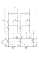
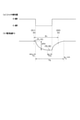
- FIG. 1 is a circuit diagram showing a power supply system 90 of the present embodiment.
- the power supply system 90 is installed in, for example, a hybrid vehicle or an electric vehicle.
- the power supply system 90 includes an assembled battery 20 and a battery monitoring device 80 for monitoring the assembled battery 20.
- the assembled battery 20 supplies power to various electric loads such as a traveling electric motor (not shown).
- the assembled battery 20 has a series connection body of a plurality of battery cells 22.
- the battery cell 22 is, for example, a lithium ion battery or the like.
- the assembled battery 20 has a plurality of detected terminals 20e.
- the detected terminals 20e other than the highest potential side and the lowest potential side are provided between the two battery cells 22 adjacent to each other in series, and are provided on the high potential side of the two battery cells 22. It is electrically connected to the negative electrode terminal of the battery cell 22 and the positive electrode terminal of the battery cell 22 on the low potential side.
- the detected terminal 20e on the highest potential side is electrically connected to the positive electrode terminal of the battery cell 22 on the highest potential side, and the detected terminal 20e on the lowest potential side is the battery on the lowest potential side. It is electrically connected to the negative electrode terminal of the cell 22.
- electrically connected is simply referred to as “connected”.
- the battery monitoring device 80 includes a discharge circuit 30, a low-pass filter circuit 40, a detection circuit 50, a drive circuit 60, and an ECU 70.
- the battery monitoring device 80 has a plurality of detection terminals 80e. Each detection terminal 80e is connected to the detected terminal 20e corresponding to itself via a harness 25.
- the plurality of harnesses 25 are modularized, and one end of each of the plurality of harnesses 25 is collectively connected to the corresponding terminal 20e to be detected, and the other ends of the plurality of harnesses 25 correspond to each other. It can be collectively connected to the detection terminals 80e.
- Each harness 25 is elongated and has a certain degree of electrical resistance value R1.
- the discharge circuit 30 is provided corresponding to each battery cell 22.
- Each discharge circuit 30 has a discharge switch 31 and a discharge resistance 32 in this order from the high potential side.
- the discharge switch 31 is a P-channel MOSFET (Metal Oxide Semiconductor Field Effect Transistor).
- the source of the discharge switch 31 is connected to the positive electrode terminal of the battery cell 22 via the harness 25 on the high potential side, and the drain of the discharge switch 31 is connected to the battery cell 22 via the discharge resistance 32 and the harness 25 on the low potential side. It is connected to the negative electrode terminal.
- the harness 25 on the low potential side for each discharge switch 31 is also used as the harness 25 on the high potential side for the discharge switch 31 on the lower potential side than the discharge switch 31.
- the drive circuit 60 is provided corresponding to each battery cell 22. Each drive circuit 60 is connected in parallel to the discharge switch 31 corresponding to itself, and operates the discharge switch 31 on or off. Specifically, the end portion 61 on the high potential side of the drive circuit 60 is connected to the terminal on the high potential side of the discharge switch 31 via the voltage dividing resistor 66 on the high potential side, and is connected to the terminal on the low potential side of the drive circuit 60. The end portion 62 is connected to the terminal on the low potential side of the discharge resistance 32 via the voltage dividing resistor 66 on the low potential side. The low potential side voltage dividing resistance 66 for each drive circuit 60 is also used as the high potential side voltage dividing resistance 66 for the drive circuit 60 on the lower potential side than the drive circuit 60.
- connection portion between the voltage dividing resistor 66 and the drive circuit 60 is connected to the gate of the discharge switch 31 via the gate resistor 67.
- the drive circuit 60 makes it impossible to energize the end portion 61 on the high potential side and the end portion 62 on the low potential side.
- the source potential and the gate potential of the discharge switch 31 become equal to the positive electrode potential of the battery cell 22 corresponding to the discharge switch 31, and the discharge switch 31 is turned off.
- the drive circuit 60 energizes the end portion 61 on the high potential side and the end portion 62 on the low potential side.
- the battery passes from the positive electrode terminal of the battery cell 22 through the harness 25 on the high potential side, the voltage dividing resistor 66 on the high potential side, the drive circuit 60, the voltage dividing resistor 66 on the low potential side, and the harness 25 on the low potential side.
- a closed circuit leading to the negative electrode terminal of the cell 22 is formed.
- the potential of the connection portion between the voltage dividing resistor 66 and the drive circuit 60 decreases, and the gate potential decreases.
- the gate potential becomes lower than the source potential by a threshold value or more, and the discharge switch 31 is turned on.
- the discharge switch 31 When the discharge switch 31 is turned on, it closes from the positive electrode terminal of the battery cell 22 to the negative electrode terminal of the battery cell 22 via the harness 25 on the high potential side, the discharge switch 31, the discharge resistance 32, and the harness 25 on the low potential side. A circuit is formed and the battery cell 22 is discharged.
- the low-pass filter circuit 40 is provided corresponding to each battery cell 22, and the input side 41 of the low-pass filter circuit 40 is connected to the discharge circuit 30. Specifically, the low-pass filter circuit 40 has a series connection body of the filter resistance 42 and the capacitor 44, and is connected in parallel to the discharge circuit 30. The low-pass filter circuit 40 removes noise above the frequency corresponding to the capacitance of the capacitor 44.
- the detection circuit 50 is connected to the output side 43 of the low-pass filter circuit 40, and detects the output voltage of the low-pass filter circuit 40 as the voltage detection value Vd. Specifically, the detection circuit 50 is connected in parallel to the series connection body of the capacitor 44 and the voltage dividing resistor 66 on the low potential side, and the voltage between the terminals of the series connection body is used as the voltage detection value Vd. Detect and transmit to ECU 70.
- the detection circuit 50 performs periodic detection Dd for detecting the voltage of each battery cell 22 in a predetermined detection cycle Dt.
- the detection cycle Dt is, for example, 20 ⁇ s or the like.
- the ECU 70 transmits an equalization command to the drive circuit 60.
- each drive circuit 60 executes a discharge for suppressing the variation under the control of the discharge switch 31.
- the discharge switch 31 for example, among the battery cells 22, the battery cells 22 other than the battery cell 22 having the lowest voltage are discharged until the voltage of the battery cell 22 having the lowest voltage is reached.
- the discharge is performed, for example, by transmitting an on-operation command to each drive circuit 60 for a corresponding time by the ECU 70.
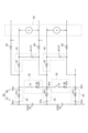
- FIG. 2 is a circuit diagram showing a state in which each discharge switch 31 is turned off.
- each discharge switch 31 which is a semiconductor switch is schematically indicated by a symbol of a normal mechanical switch for visibility of the on state / off state of each discharge switch 31. There is.
- the one on the high potential side is referred to as "upper battery cell 22A”, and the one on the low potential side is referred to as “lower battery cell 22B”.
- the discharge circuit 30 corresponding to the upper battery cell 22A is referred to as an "upper discharge circuit 30”
- the discharge circuit 30 corresponding to the lower battery cell 22B is referred to as a "lower discharge circuit 30”.
- the discharge switch 31 of the upper discharge circuit 30 is referred to as an "upper discharge switch 31”
- the discharge switch 31 of the lower discharge circuit 30 is referred to as a "lower discharge switch 31".
- the capacitor 44 corresponding to the upper battery cell 22B is referred to as the "upper capacitor 44”
- the capacitor 44 corresponding to the lower battery cell 22B is referred to as the “lower capacitor 44”.
- the voltage detection value Vd corresponding to the upper battery cell 22A is set to "upper voltage detection value Vd”
- the voltage detection value Vd corresponding to the lower battery cell 22B is set to "lower voltage detection value Vd”.
- each capacitor 44 is charged until the voltage between its terminals becomes the same as the voltage Vc between terminals of the battery cell 22 corresponding to itself.
- This state will be referred to as "off steady state” below.
- the voltage detection value Vd by the detection circuit 50 becomes equal to the terminal-to-terminal voltage Vc of the corresponding battery cell 22. Therefore, in the periodic detection Dd, the voltage detection value Vd can be adopted as the inter-terminal voltage Vc of the corresponding battery cell 22.
- the discharge switch 31 may have an abnormality such as an on-sticking abnormality or an off-sticking abnormality. Therefore, in the present embodiment, the ECU 70 performs switch diagnosis for diagnosing the presence or absence of abnormality in the discharge switch 31. Therefore, the ECU 70 also serves as a diagnostic unit for performing switch diagnosis, and the battery monitoring device 80 also serves as a diagnostic device including the diagnostic unit.
- the switch diagnosis is performed between two consecutive periodic detections Dd. In the switch diagnosis, a diagnostic operation is performed in which the discharge switch 31 to be diagnosed is switched from the off operation to the on operation and then switched to the off operation again. Next, the switch diagnosis will be described.
- FIG. 3 is a circuit diagram showing a state in which the upper discharge switch 31 is being operated for diagnosis. Specifically, the upper discharge switch 31 is turned on and the lower discharge switch 31 is turned on. It is a circuit diagram which shows the state which the 31 is turned off.
- the switch diagnosis is performed for each of the discharge switches 31 odd-numbered from the high potential side, and then for each of the discharge switches 31 even-numbered from the high potential side. Perform switch diagnosis. This is because when all the discharge switches 31 are turned on at the same time, the positive electrode terminal of the uppermost battery cell 22 is short-circuited to the negative electrode terminal of the lowermost battery cell 22. Therefore, for example, the switch diagnosis is performed on the upper discharge switch 31, and then the switch diagnosis is performed on the lower discharge switch 31.
- the state in which the discharge switch 31 is switched from the off state to the on state and the voltage detection value Vd is completely lowered is referred to as an "on steady state".
- the voltage detection value Vd in the on-steady state is as shown in the following formula 1 when the electric resistance in the discharge switch 31 and the electric resistance in the wiring other than the harness 25 are ignored.
- Vd Vc ⁇ R2 / (2R1 + R2) (Formula 1)
- Vc the voltage between the terminals of the battery cell 22
- R1 the electric resistance value of the harness 25
- R2 the electric resistance value of the discharge resistance 32.
- the voltage detection value Vd in the off steady state is the voltage Vc between the terminals of the battery cell 22 as described above. Therefore, the “voltage change amount ⁇ Vo”, which is the difference between the voltage detection value Vd in the off-steady state and the voltage detection value Vd in the on-steady state, is as shown in Equation 2 below.
- ⁇ Vo Vc ⁇ 2R1 / (2R1 + R2) (Formula 2) Therefore, when the discharge switch 31 is switched from the on operation to the off operation in the normal state, the voltage detection value Vd changes by the above voltage change amount ⁇ Vo. On the other hand, in a state where the discharge switch 31 has an on-stick failure or an off-stick failure, the amount of change in the voltage detection value Vd is smaller than the above-mentioned voltage change amount ⁇ Vo. Therefore, in the switch diagnosis, it is determined whether or not the discharge switch 31 is abnormal based on the difference.
- the upper discharge switch 31 When the upper discharge switch 31 is turned on, not only the upper voltage detection value Vd but also the lower voltage detection value Vd fluctuates. This is because, as described above, the harness 25 on the low potential side for the upper discharge switch 31 and the harness 25 on the high potential side for the lower discharge switch 31 are shared. Specifically, when the upper discharge switch 31 is switched from the off operation to the on operation, the potential of the connection portion between the harness 25 on the high potential side and the filter resistance 42 for the lower discharge switch 31 becomes the harness 25. It rises by the voltage between the terminals of. As a result, the lower capacitor 44 is charged, and the lower voltage detection value Vd rises.
- the switch diagnosis for the upper discharge switch 31 is performed within one detection cycle Dt, and the switch diagnosis for the lower discharge switch 31 is performed within the other detection cycle Dt. There is.
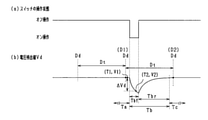
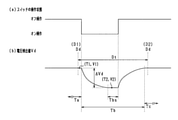
- FIG. 4 is a time chart showing the transition of each value in the switch diagnosis when the discharge switch 31 is normal. More specifically, FIG. 4A is a time chart showing the transition of the state of the discharge switch 31, and FIG. 4B is a graph showing the transition of the voltage detection value Vd at that time.
- the drive circuit 60 executes a diagnostic operation according to a command from the ECU 70.
- the diagnostic operation as shown in FIG. 4A, the drive circuit 60 switches the discharge switch 31 from an off operation to an on operation, and then, as shown in FIG. 4B, the voltage detection value Vd is set. Before it stabilizes, the discharge switch 31 is switched off again as shown in FIG. 4A.
- this diagnostic operation is performed between two consecutive periodic detections Dd, as shown in FIG. 4 (b).
- the front side of the two periodic detections Dd will be referred to as “front periodic detection D1”, and the rear side will be referred to as “rear periodic detection D2”.
- the voltage detection value Vd is stabilized by the periodic detection D2 on the rear side. Therefore, after the voltage detection value Vd becomes stable, the periodic detection D2 on the rear side is performed.
- the voltage detection value Vd here is stable when the voltage detection value Vd converges to the voltage between terminals Vc of the battery cell 22, and more specifically, for example, the current voltage detection value Vd.
- the difference between the voltage detection value Vd and the voltage detection value Vd in the off steady state is 1% or less of the voltage change amount ⁇ Vo.
- pre-variation period Ta The period from when the discharge switch 31 is switched from the off operation to the on operation by the diagnostic operation until the discharge switch 31 is switched to the off operation again and the voltage detection value Vd stabilizes is referred to as "variable period Tb". do. Then, the period after the stable timing is referred to as "post-change period Tc".
- the period before the discharge switch 31 in the variable period Tb is switched to the off operation again is defined as "the first half Tbf of the variable period”.
- the period after the discharge switch 31 in the variable period Tb is switched to the off operation again is referred to as "the latter half Tbr of the variable period”.
- the detection cycle Dt is smaller than 9.2 times the time constant (R ⁇ C).
- 4.6 times the time constant (R ⁇ C) is the difference between the current voltage detection value Vd and the voltage detection value Vd in the on steady state when switching from the off steady state to the on state. It is the time to become 1% of the amount of change ⁇ Vo. That is, 4.6 times this time constant (R ⁇ C) is the time required for the voltage to stabilize when the off steady state is switched to the on state.
- the voltage detection value Vd in the pre-variation period Ta is adopted as the first detection value V1.
- the first detection value V1 may be the voltage detection value Vd detected by the periodic detection D1 on the front side, or may be the voltage detection value Vd independently detected for switch diagnosis.
- FIG. 4B shows a case where the detection is unique.
- the drive circuit 60 switches the discharge switch 31 from the off operation to the on operation as shown in FIG. 4A.
- the voltage detection value Vd decreases.
- the voltage detection value Vd does not decrease at once, but decreases in a curved shape in a form in which the voltage decrease rate gradually decreases according to the following equation 4.
- Vd Vc- ⁇ Vo (1-EXP (-T / (R ⁇ C))) (Formula 4)
- Vc is the voltage Vc between the terminals of the battery cell 22
- ⁇ Vo is the voltage change amount ⁇ Vo
- T is the elapsed time T since the discharge switch 31 is switched on.
- R ⁇ C is a time constant.
- the voltage detection value Vd decreases according to the above formula 4. Then, the detection circuit 50 detects the voltage at the second timing T2 within the first half Tbf of the fluctuation period.
- the second timing T2 is a timing at which a predetermined time or more has elapsed since the discharge switch 31 was switched from the off operation to the on operation. Then, the ECU 70 adopts the voltage detection value Vd at the second timing T2 as the second detection value V2.
- the optimum timing can be obtained in advance by an experiment or a calculation based on the circuit characteristics, and the optimum timing can be set as the second timing T2.
- the second timing T2 may be stored in a memory of the ECU 70, a memory connected to the ECU 70, or the like.
- the discharge switch 31 is switched from the on operation to the off operation again.
- the voltage detection value Vd rises.
- the voltage detection value Vd does not increase at once, but increases in a curved shape in a form in which the voltage increase rate gradually decreases.
- the ECU 70 After acquiring the second detection value V2, the ECU 70 performs switch diagnosis based on the first detection value V1 and the second detection value V2. Specifically, if the detection value change amount ⁇ Vd, which is the difference between the first detection value V1 and the second detection value V2, is equal to or greater than a predetermined change threshold value, it is determined that the discharge switch 31 is normal, and the detection value change. If the amount ⁇ Vd is less than the change threshold value, the discharge switch 31 determines that it is abnormal. This change threshold is set smaller than the case where the voltage detection value Vd is sufficiently lowered in view of switching the discharge switch 31 from the on operation to the off operation again before the voltage detection value Vd is sufficiently lowered.
- the ECU 70 determines that the discharge switch 31 is abnormal in the switch diagnosis, the ECU 70 notifies the upper ECU that the discharge switch 31 is abnormal. As a result, a predetermined fail-safe process is executed.
- the battery monitoring device 80 includes a low-pass filter circuit 40, the input side 41 of the low-pass filter circuit 40 is connected to the battery cell 22, and the output side 43 is connected to the detection circuit 50. Therefore, noise from the battery cell 22 to the detection circuit 50 can be removed.
- the switch diagnosis in the switch diagnosis, the first detection value V1 at the first timing T1 before switching from the off operation to the on operation and the second timing T2 after a predetermined time has elapsed after switching to the on operation. Based on the second detection value V2 of the above, it is determined whether or not the discharge switch 31 is abnormal. Therefore, a waiting time for waiting for the voltage detection value Vd to change is secured between the first timing T1 and the second timing T2 for a predetermined time. Therefore, it is possible to suppress an erroneous determination in the switch diagnosis based on the fact that the change in the voltage detection value Vd is delayed by the capacitor 44.
- the drive circuit 60 switches the discharge switch 31 from the off operation to the on operation, and then switches the discharge switch 31 to the off operation again before the voltage detection value Vd stabilizes. Therefore, the voltage detection value Vd can be quickly returned to the original state as compared with the case where the voltage detection value Vd is stabilized and then switched to the off operation again, and the power consumption of the battery cell 22 and the inside of the battery monitoring device 80 can be obtained. It is possible to reduce heat generation and element deterioration in the device.
- the first timing T1 is the timing within the pre-variation period Ta
- the second timing T2 is the timing within the first half Tbf of the fluctuation period. Therefore, the first detection value V1 and the second detection value V2 are aligned at the second timing T2 of the first half of the fluctuation period Tbf, and the switch diagnosis can be performed quickly.
- the detection circuit 50 performs periodic detection Dd for detecting the voltage of each battery cell 22 in a predetermined detection cycle Dt. Therefore, it is preferable that the diagnostic operation is performed between two consecutive periodic detections Dd, and the voltage detection value Vd is stable by the rear periodic detection D2. In that respect, in the present embodiment, as described above, the voltage detection value Vd can be quickly returned to the original state, whereby the voltage detection value Vd can be stabilized by the periodic detection D2 on the rear side.
- the detection cycle Dt is 9.2 times the time constant (R ⁇ C), that is, the discharge switch 31 is turned on to stabilize the voltage detection value Vd, and then the discharge switch. It is shorter than the minimum time required for a series of operations to stabilize the voltage detection value Vd by turning off 31 again. Therefore, if the voltage detection value Vd is waiting to stabilize, the fluctuation period Tb does not fall within one detection cycle Dt.
- the discharge switch 31 is switched to the off operation again to quickly return the voltage detection value Vd to the original state. As a result, the fluctuation period Tb is kept within one detection cycle Dt. Therefore, when the detection cycle Dt of the battery monitoring device 80 is short as described above, the present embodiment can be preferably implemented.
- the diagnostic operation is executed on the upper discharge switch 31, and then the diagnostic operation is executed on the other lower discharge switch 31. Then, when the diagnostic operation is executed for the upper discharge switch 31, the charge amount of the lower capacitor 44 changes. Therefore, it is necessary to include the fluctuation of the lower voltage detection value Vd due to the diagnostic operation for the upper discharge switch 31 performed earlier until the diagnostic operation for the lower discharge switch 31 performed next.
- the voltage detection value Vd can be quickly returned to the original state, so that the lower voltage detection value by the diagnostic operation for the upper discharge switch 31 performed earlier is performed. The fluctuation of Vd can be easily contained in the next diagnostic operation for the lower discharge switch 31.
- the ECU 70 determines that the discharge switch 31 is abnormal on condition that the detection value change amount ⁇ Vd, which is the difference between the first detection value V1 and the second detection value V2, is equal to or less than the change threshold value. Therefore, it is possible to determine whether or not the discharge switch 31 is abnormal by a simple method.
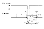
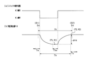
- FIG. 5 is a time chart showing the transition of each value in the switch diagnosis when the discharge switch 31 is normal. More specifically, FIG. 5A is a time chart showing the transition of the state of the discharge switch 31, and FIG. 5B is a graph showing the transition of the voltage detection value Vd at that time.
- the first timing T1 for detecting the first detection value V1 is not within the pre-variation period Ta but within the fluctuation period Tb.
- the second timing T2 for detecting the second detection value V2 is not within the fluctuation period Tb but within the post-variation period Tc.
- the voltage detection value Vd in the periodic detection D2 on the rear side may be diverted, or may be independently detected in the switch diagnosis.
- FIG. 5B shows a case where the detection is unique.
- the switch diagnosis is delayed by the amount that the timing at which the first detection value V1 and the second detection value V2 are aligned is later than that in the case of the first embodiment, but other than that, the switch diagnosis is delayed.
- the same effect as in the case of the first embodiment can be obtained.
- FIG. 6 is a time chart showing the transition of each value in the switch diagnosis when the discharge switch 31 is normal. More specifically, FIG. 6A is a time chart showing the transition of the state of the discharge switch 31, and FIG. 6B is a graph showing the transition of the voltage detection value Vd at that time.
- the detection cycle Dt is 9.2 times the time constant (R ⁇ C), that is, the discharge switch 31 is turned on to stabilize the voltage detection value Vd, and then the discharge switch 31 is turned off again. It is longer than the minimum time required for a series of operations to stabilize the voltage detection value Vd. Then, in the diagnostic operation, the discharge switch 31 is switched from the off operation to the on operation, and then the discharge switch 31 is turned off again after the voltage detection value Vd stabilizes, not before the voltage detection value Vd stabilizes. Switch to.
- stable period Tbs the period from when the discharge switch 31 is switched to the on operation and the voltage detection value Vd is stabilized by the diagnostic operation until the discharge switch 31 is switched to the off operation again.
- the voltage detection value Vd here is stable means that the voltage detection value Vd converges to the voltage detection value Vd in the on steady state, and more specifically, for example, the current voltage detection value Vd.
- the difference between the voltage detection value Vd and the voltage detection value Vd in the on-steady state is 1% or less of the voltage change amount ⁇ Vo.
- the first timing T1 for detecting the first detection value V1 is within the pre-variation period Ta as in the case of the first embodiment, but the second timing T2 for detecting the second detection value V2 is the stable period Tbs. Within. Specifically, it is as follows.
- the voltage detection value Vd at the first timing T1 within the pre-variation period Ta is adopted as the first detection value V1. do.
- the discharge switch 31 is switched from the off operation to the on operation.
- the voltage detection value Vd decreases.
- the voltage detection value Vd does not decrease at once, but decreases according to the above equation 4. Up to this point, the same as in the case of the first embodiment.
- the voltage detection value Vd is adopted as the second detection value V2. Then, as shown in FIG. 6A, the discharge switch 31 is switched from the on operation to the off operation again.
- the ECU 70 calculates the detection value change amount ⁇ Vd which is the difference between the first detection value V1 and the second detection value V2. It is determined whether or not the detected value change amount ⁇ Vd is larger than the predetermined change threshold value.
- the change threshold value here is larger than the change threshold value in the first embodiment. This is because the amount of change in the detected value ⁇ Vd in the normal state is larger than in the case of the first embodiment. Then, if the detected value change amount ⁇ Vd is larger than the change threshold value, it is determined that the discharge switch 31 is normal, and if the detected value change amount ⁇ Vd is smaller than the change threshold value, it is determined that the discharge switch 31 is abnormal.
- the switch diagnosis the discharge switch 31 is switched from the off operation to the on operation, and then, after the voltage detection value Vd stabilizes, the discharge switch 31 is switched to the off operation again.
- the second timing T2 for detecting the second detection value V2 is the timing within the stable period Tbs. Therefore, although it takes longer to diagnose the switch than in the first embodiment, the switch diagnosis can be performed based on the voltage detection value Vd at the time of stabilization, and the switch diagnosis can be performed based on the voltage detection value Vd before stabilization.
- the switch diagnosis can be performed more accurately than when it is performed. Therefore, this embodiment can be preferably implemented when the detection cycle Dt is relatively long.
- FIG. 7 is a time chart showing the transition of each value in the switch diagnosis when the discharge switch 31 is normal. More specifically, FIG. 7A is a time chart showing the transition of the state of the discharge switch 31, and FIG. 7B is a graph showing the transition of the voltage detection value Vd at that time.
- the first timing T1 for detecting the first detection value V1 is not within the pre-variation period Ta but within the stable period Tbs.
- the second timing T2 for detecting the second detection value V2 is not within the stable period Tbs but within the post-variation period Tc.
- the timing at which the first detection value V1 and the second detection value V2 are aligned is later than that in the case of the third embodiment, but other than that, it is the same as in the case of the third embodiment. The effect of is obtained.
- FIG. 8 is a time chart showing the transition of each value in the switch diagnosis when the discharge switch 31 is normal. More specifically, FIG. 8A is a time chart showing the transition of the state of the discharge switch 31, and FIG. 8B is a graph showing the transition of the voltage detection value Vd at that time.
- the detection cycle Dt is 9.2 times the time constant (R ⁇ C), that is, the discharge switch 31 is turned on to stabilize the voltage detection value Vd, and then the discharge switch 31 is turned off again. It is shorter than the minimum time required for a series of operations to stabilize the voltage detection value Vd. Therefore, as shown in FIG. 8B, the fluctuation period Tb in the switch diagnosis does not fall within one detection cycle Dt. Therefore, the periodic detection D2 on the rear side is performed before the voltage detection value Vd becomes stable. Therefore, it corresponds by correcting the voltage detection value Vd in the periodic detection D2 on the rear side. The correction may be performed, for example, based on a calculation or a map.
- the switch diagnosis can be performed even when the fluctuation period Tb does not fall within one detection cycle Dt. ..
- FIG. 9 is a circuit diagram showing the battery monitoring device 80 of the present embodiment and its surroundings.
- the battery monitoring device 80 includes a noise removing element 26 that is interposed between the detection terminal 80e and the discharge circuit 30 to remove noise.
- the noise reducing element 26 has, for example, a coil or the like. Then, when the discharge switch 31 is switched from the off operation to the on operation, the voltage detection value Vd is lowered due to the impedance of the noise reduction element 26.
- the switch diagnosis can be performed by effectively utilizing the impedance of the noise reduction element 26.
- This diagnosis is effective when, for example, the harness 25 is sufficiently thick and the electrical resistance of the harness 25 is small.
- FIG. 10 is a circuit diagram showing the battery monitoring device 80 of the present embodiment and its surroundings.
- the battery monitoring device 80 includes an overcurrent protection element 27 for preventing an overcurrent from flowing between the detection terminal 80e and the discharge circuit 30.
- the overcurrent protection element 27 is, for example, a fuse or the like. Then, when the discharge switch 31 is switched from the off operation to the on operation, the voltage detection value Vd is lowered due to the impedance of the overcurrent protection element 27.
- the switch diagnosis can be performed by effectively utilizing the impedance of the overcurrent protection element 27. This diagnosis is effective when, for example, the harness 25 is sufficiently thick and the electrical resistance of the harness 25 is small.
- the switch diagnosis is performed based on the detection value change amount ⁇ Vd, which is the difference between the first detection value V1 and the second detection value V2.
- the switch diagnosis may be performed based on the ratio of the first detection value V1 and the second detection value V2. Specifically, for example, when the second detection value V2 in the normal state is smaller than the first detection value V1 in the normal state, the ratio of the second detection value V2 to the first detection value V1 is larger than the threshold value. On the condition that the discharge switch 31 is abnormal, it may be determined.
- the diagnostic operation may be performed a plurality of times for each discharge switch 31, and the switch diagnosis may be performed based on the voltage detection value Vd in the plurality of diagnostic operations.
- the discharge switch 31 may be determined to be abnormal on the condition that the average value of the detected value change amount ⁇ Vd in the plurality of diagnostic operations is below the change threshold value. Further, for example, the discharge switch 31 may be determined to be abnormal on the condition that it is continuously determined that the detected value change amount ⁇ Vd is below the change threshold value in each of the plurality of diagnostic operations. According to these forms, the discharge switch 31 can be diagnosed more accurately.
- the discharge switch 31 is a MOSFET, but instead of this, an IGBT (Insulated Gate Bipolar Transistor), another bipolar transistor, or the like may be used.
- IGBT Insulated Gate Bipolar Transistor
- the second timing T2 is the timing within the first half Tbf of the fluctuation period, but instead of this, the timing may be within the second half Tbr of the fluctuation period.
Landscapes
- Engineering & Computer Science (AREA)
- Manufacturing & Machinery (AREA)
- Chemical & Material Sciences (AREA)
- Chemical Kinetics & Catalysis (AREA)
- Electrochemistry (AREA)
- General Chemical & Material Sciences (AREA)
- Power Engineering (AREA)
- Secondary Cells (AREA)
- Charge And Discharge Circuits For Batteries Or The Like (AREA)
Priority Applications (1)
| Application Number | Priority Date | Filing Date | Title |
|---|---|---|---|
| CN202180058000.5A CN116057753A (zh) | 2020-08-03 | 2021-07-07 | 诊断装置 |
Applications Claiming Priority (2)
| Application Number | Priority Date | Filing Date | Title |
|---|---|---|---|
| JP2020131693A JP2022028348A (ja) | 2020-08-03 | 2020-08-03 | 診断装置 |
| JP2020-131693 | 2020-08-03 |
Publications (1)
| Publication Number | Publication Date |
|---|---|
| WO2022030168A1 true WO2022030168A1 (ja) | 2022-02-10 |
Family
ID=80119761
Family Applications (1)
| Application Number | Title | Priority Date | Filing Date |
|---|---|---|---|
| PCT/JP2021/025576 Ceased WO2022030168A1 (ja) | 2020-08-03 | 2021-07-07 | 診断装置 |
Country Status (3)
| Country | Link |
|---|---|
| JP (1) | JP2022028348A (enExample) |
| CN (1) | CN116057753A (enExample) |
| WO (1) | WO2022030168A1 (enExample) |
Cited By (1)
| Publication number | Priority date | Publication date | Assignee | Title |
|---|---|---|---|---|
| WO2023207430A1 (zh) * | 2022-04-24 | 2023-11-02 | 宁德时代新能源科技股份有限公司 | 一种开关装置、电机控制装置及电池加热系统 |
Citations (3)
| Publication number | Priority date | Publication date | Assignee | Title |
|---|---|---|---|---|
| JP2004266992A (ja) * | 2003-02-10 | 2004-09-24 | Denso Corp | 組電池の放電装置 |
| JP2014196951A (ja) * | 2013-03-29 | 2014-10-16 | 株式会社ケーヒン | 電圧検出装置 |
| JP2019114464A (ja) * | 2017-12-25 | 2019-07-11 | 株式会社デンソー | 監視装置 |
-
2020
- 2020-08-03 JP JP2020131693A patent/JP2022028348A/ja active Pending
-
2021
- 2021-07-07 WO PCT/JP2021/025576 patent/WO2022030168A1/ja not_active Ceased
- 2021-07-07 CN CN202180058000.5A patent/CN116057753A/zh active Pending
Patent Citations (3)
| Publication number | Priority date | Publication date | Assignee | Title |
|---|---|---|---|---|
| JP2004266992A (ja) * | 2003-02-10 | 2004-09-24 | Denso Corp | 組電池の放電装置 |
| JP2014196951A (ja) * | 2013-03-29 | 2014-10-16 | 株式会社ケーヒン | 電圧検出装置 |
| JP2019114464A (ja) * | 2017-12-25 | 2019-07-11 | 株式会社デンソー | 監視装置 |
Cited By (1)
| Publication number | Priority date | Publication date | Assignee | Title |
|---|---|---|---|---|
| WO2023207430A1 (zh) * | 2022-04-24 | 2023-11-02 | 宁德时代新能源科技股份有限公司 | 一种开关装置、电机控制装置及电池加热系统 |
Also Published As
| Publication number | Publication date |
|---|---|
| JP2022028348A (ja) | 2022-02-16 |
| CN116057753A (zh) | 2023-05-02 |
Similar Documents
| Publication | Publication Date | Title |
|---|---|---|
| CN103718449B (zh) | 电力转换装置 | |
| US9562949B2 (en) | Battery monitoring device | |
| JP5597349B2 (ja) | 組電池の接続異常診断装置 | |
| WO2013190733A1 (ja) | リーク検出装置 | |
| US11329474B2 (en) | Switching controller with adaptive overheating protection | |
| CN106458041B (zh) | 车辆用接地检测装置 | |
| JP6494327B2 (ja) | 劣化検出装置および劣化検出方法 | |
| US20170244259A1 (en) | Voltage detecting device | |
| EP4130765B1 (en) | Ground fault detection device | |
| US11223195B2 (en) | Control device and method for power supply to EPS in vehicle | |
| JPWO2016143679A1 (ja) | 電池管理装置、電池監視回路、制御システム | |
| WO2018230187A1 (ja) | 電池監視装置 | |
| US10161980B2 (en) | Deterioration detecting apparatus and deterioration detecting method | |
| US8963524B2 (en) | Drive circuit for switching elements | |
| US9444446B2 (en) | Switching control circuit for target switching element | |
| JP6787705B2 (ja) | 異常検出装置、および組電池システム | |
| WO2022030168A1 (ja) | 診断装置 | |
| CN111033288B (zh) | 异常检测装置 | |
| JP6322123B2 (ja) | 電流制限回路 | |
| US20160380557A1 (en) | Assembly and method for discharging high-voltage circuit of power inverter | |
| CN119010544A (zh) | 主动放电电路和电力转换装置 | |
| JP5316343B2 (ja) | 電池監視装置 | |
| US20260011999A1 (en) | Vehicle cutoff device | |
| JP7799936B2 (ja) | 車載用電源装置 | |
| WO2024116752A1 (ja) | 車載用電源装置 |
Legal Events
| Date | Code | Title | Description |
|---|---|---|---|
| 121 | Ep: the epo has been informed by wipo that ep was designated in this application |
Ref document number: 21852345 Country of ref document: EP Kind code of ref document: A1 |
|
| NENP | Non-entry into the national phase |
Ref country code: DE |
|
| 122 | Ep: pct application non-entry in european phase |
Ref document number: 21852345 Country of ref document: EP Kind code of ref document: A1 |