WO2022030167A1 - 電力変換器の制御回路 - Google Patents
電力変換器の制御回路 Download PDFInfo
- Publication number
- WO2022030167A1 WO2022030167A1 PCT/JP2021/025575 JP2021025575W WO2022030167A1 WO 2022030167 A1 WO2022030167 A1 WO 2022030167A1 JP 2021025575 W JP2021025575 W JP 2021025575W WO 2022030167 A1 WO2022030167 A1 WO 2022030167A1
- Authority
- WO
- WIPO (PCT)
- Prior art keywords
- voltage
- unit
- abnormality
- control
- control circuit
- Prior art date
- Legal status (The legal status is an assumption and is not a legal conclusion. Google has not performed a legal analysis and makes no representation as to the accuracy of the status listed.)
- Ceased
Links
Images


Classifications
-
- H—ELECTRICITY
- H02—GENERATION; CONVERSION OR DISTRIBUTION OF ELECTRIC POWER
- H02M—APPARATUS FOR CONVERSION BETWEEN AC AND AC, BETWEEN AC AND DC, OR BETWEEN DC AND DC, AND FOR USE WITH MAINS OR SIMILAR POWER SUPPLY SYSTEMS; CONVERSION OF DC OR AC INPUT POWER INTO SURGE OUTPUT POWER; CONTROL OR REGULATION THEREOF
- H02M7/00—Conversion of AC power input into DC power output; Conversion of DC power input into AC power output
- H02M7/42—Conversion of DC power input into AC power output without possibility of reversal
- H02M7/44—Conversion of DC power input into AC power output without possibility of reversal by static converters
- H02M7/48—Conversion of DC power input into AC power output without possibility of reversal by static converters using discharge tubes with control electrode or semiconductor devices with control electrode
Definitions
- the present disclosure relates to a control circuit of a power converter having a switch of an upper and lower arm electrically connected to the winding of each phase of a rotary electric machine.
- Patent Document 1 discloses a circuit including a voltage detection unit and an abnormality determination unit.
- the voltage detection unit detects the output voltage of the power storage unit and outputs it to the abnormality determination unit.
- the abnormality determination unit determines that an overvoltage abnormality has occurred in the system.
- An abnormality that makes it impossible to determine an overvoltage abnormality may occur.
- the following problems occur.
- the control circuit implements short-circuit control to turn on the switch in one of the upper and lower arms and turn off the switch in the other arm in order to deal with the case where an overvoltage abnormality occurs in the system.
- short-circuit control will not be performed even though the short-circuit control should be performed.
- the present disclosure has been made in view of the above circumstances, and an object thereof is to provide a control circuit of a power converter capable of determining that an abnormality that cannot determine an overvoltage abnormality has occurred.
- the present disclosure comprises a power storage unit, a multi-phase rotary electric machine, and a power converter having a switch of an upper and lower arm electrically connected to the winding of each phase of the rotary electric machine and the power storage unit.
- a control circuit of the power converter applied to it is determined that an overvoltage abnormality has occurred in the system because the voltage detection unit that detects the output voltage of the power storage unit and the detection voltage of the voltage detection unit cross the threshold value.
- An abnormality determination unit and a processing unit that performs pseudo-abnormality processing so that the detection voltage of the voltage detection unit crosses the threshold when the detection voltage of the voltage detection unit does not exceed the threshold. Be prepared.
- a state in which an overvoltage abnormality is determined to have occurred in the system is simulated by the abnormality determination unit by performing the pseudo-abnormality processing.
- FIG. 1 is an overall configuration diagram of a control system according to the first embodiment.
- FIG. 2 is a diagram showing a control circuit and its peripheral configuration.
- FIG. 3 is a diagram showing an example of the configuration of the high voltage detection circuit.
- FIG. 4 is a diagram showing a control circuit in a comparative example.
- FIG. 5 is a time chart showing an example of control performed by the control circuit of the comparative example.
- FIG. 6 is a diagram showing a control circuit.
- FIG. 7 is a flowchart showing a procedure of processing performed by the microcomputer.
- FIG. 8 is a diagram showing a control circuit according to the second embodiment.
- FIG. 1 is an overall configuration diagram of a control system according to the first embodiment.
- FIG. 2 is a diagram showing a control circuit and its peripheral configuration.
- FIG. 3 is a diagram showing an example of the configuration of the high voltage detection circuit.
- FIG. 4 is a diagram showing a control circuit in a comparative example.
- FIG. 5 is
- FIG. 9 is a flowchart showing a procedure of processing performed by the microcomputer.
- FIG. 10 is a flowchart showing a procedure of processing performed by the microcomputer according to the third embodiment.
- FIG. 11 is a flowchart showing a procedure of processing performed by the microcomputer according to the fourth embodiment.
- control circuit according to the present disclosure is embodied
- the control circuit according to this embodiment is applied to a three-phase inverter as a power converter.
- the control system including the inverter is mounted on a vehicle such as an electric vehicle or a hybrid vehicle.
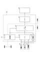
- the control system includes a rotary electric machine 10, an inverter 15, and a DCDC converter 25.
- the rotary electric machine 10 is an in-vehicle main engine, and its rotor is capable of transmitting power to drive wheels (not shown).
- a synchronous machine is used as the rotary electric machine 10, and more specifically, a permanent magnet synchronous machine is used.
- the input side of the DCDC converter 25 is connected to the high-voltage power supply 30 as a "DC power supply", boosts the output voltage of the input high-voltage power supply 30, and outputs it to the inverter 15.
- the DCDC converter 25 is controlled by the control circuit 50.
- the high voltage power supply 30 is a secondary battery, and its output voltage (rated voltage) is, for example, 100 V or more.
- the DCDC converter 25 corresponds to a "boost circuit".
- the inverter 15 includes a switching device unit 20.
- the switching device unit 20 includes a series connection body of the upper arm switch SWH and the lower arm switch SWL for three phases. In each phase, the first end of the winding 11 of the rotary electric machine 10 is connected to the connection points of the upper and lower arm switches SWH and SWL. The second end of each phase winding 11 is connected at a neutral point.
- the phase windings 11 are arranged so as to be offset by 120 ° from each other by the electric angle.
- a voltage-controlled semiconductor switching element is used as each switch SWH and SWL, and more specifically, an IGBT is used.
- the upper and lower arm diodes DH and DL which are freewheel diodes, are connected in antiparallel to the upper and lower arm switches SWH and SWL.
- the output side of the DCDC converter 25 is connected to the collector, which is the high potential side terminal of each upper arm switch SWH, via the high potential side electric path 22H.
- the output side of the DCDC converter 25 is connected to the emitter, which is the low potential side terminal of each lower arm switch SWL, via the low potential side electric path 22L.
- the high potential side electric path 22H is provided with a first cutoff switch 23a, and the low potential side electric path 22L is provided with a second cutoff switch 23b.
- Each switch 23a, 23b is, for example, a relay or a semiconductor switching element.
- the switches 23a and 23b may be driven by the control circuit 50 included in the inverter 15, or may be driven by a control device higher than the control circuit 50.
- the inverter 15 includes a smoothing capacitor 24 as a "storage unit".
- the smoothing capacitor 24 electrically connects the switching device section 20 side of the high potential side electric path 22H with respect to the first cutoff switch 23a and the switching device section 20 side of the low potential side electric path 22L with respect to the second cutoff switch 23b. Is connected.
- the control circuit 50 acquires the terminal voltage VH of the smoothing capacitor 24.
- the control system includes a phase current sensor 40 and an angle sensor 41.
- the phase current sensor 40 detects at least two phases of the U, V, and W phase currents flowing through the rotary electric machine 10.
- the angle sensor 41 outputs an angle signal according to the electric angle of the rotary electric machine 10.
- the angle sensor 41 is, for example, an MR sensor having a resolver, an encoder, or a magnetoresistive sensor, and is a resolver in this embodiment.
- control circuit 50 The configuration of the control circuit 50 will be described with reference to FIG.
- the control circuit 50 includes a microcomputer 51 provided in a low voltage region.
- the current signal of the phase current sensor 40 is input to the microcomputer 51.
- the microcomputer 51 calculates the phase current Ir based on the input current signal.
- the microcomputer 51 acquires the electric angle ⁇ e of the rotary electric machine 10.
- the control circuit 50 has an excitation circuit and a resolver digital converter (not shown).
- a sinusoidal excitation signal is supplied from the excitation circuit to the resolver stator constituting the angle sensor 41.
- the angular signal output from the resolver stator is input to the resolver digital converter.
- the resolver digital converter calculates the electric angle ⁇ e of the rotary electric machine 10 based on the angle signal and outputs it to the microcomputer 51.
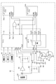
- the control circuit 50 includes a high voltage detection circuit 52 as a "voltage detection unit".
- the high voltage detection circuit 52 is provided in the low voltage region and the high voltage region across the boundary between the low voltage region and the high voltage region in the control circuit 50.
- the terminal voltage VH of the smoothing capacitor 24 is input to the high voltage region side of the high voltage detection circuit 52 via the high potential side connection point TH and the low potential side connection point TL.
- the high-voltage detection circuit 52 outputs a detection voltage VS (for example, 0 to 5V), which is a voltage obtained by stepping down the terminal voltage VH of the smoothing capacitor 24, to the microcomputer 51 on the low-voltage region side.
- a detection voltage VS for example, 0 to 5V
- FIG. 3 is an example of a circuit for stepping down the terminal voltage VH of the smoothing capacitor 24 in the high voltage detection circuit 52.
- the high voltage detection circuit 52 includes a differential amplifier circuit having an operational amplifier 70 and resistors 71 to 74, respectively.
- the high voltage detection circuit 52 has a conversion function for lowering the terminal voltage VH of the smoothing capacitor 24 to a voltage range (for example, 0 to 5 V) that can be input to the microcomputer 51. This is because, in the present embodiment, the high-voltage power supply 30 is provided in the high-voltage region, whereas the microcomputer 51 and the ASIC unit 63 are provided in the low-voltage region.
- the difference between the potential of the high potential side connection point TH and the potential of the low potential side connection point TL output from the DCDC converter 25 is divided by a plurality of high resistance bodies 71 and then input to the inverting input terminal of the operational amplifier 70. Will be done. Further, the difference between the potential of the low potential side connection point TL output from the DCDC converter 25 and the ground potential (ground potential) is divided by the plurality of high resistance bodies 72 and the low resistance body 73, and the operational amplifier 70 is divided. It is input to the non-inverting input terminal. The inverting input terminal and the output terminal of the operational amplifier 70 are connected by a resistor 74.
- the high voltage detection circuit 52 converts so that the higher the terminal voltage VH of the smoothing capacitor 24, the lower the detection voltage VS of the high voltage detection circuit 52.
- a command value is input to the microcomputer 51 from the host control device 42.
- the microcomputer 51 generates a switching command for turning on / off the switches SWH and SWL of the switching device unit 20 in order to control the control amount of the rotary electric machine 10 to the command value.
- the control amount is, for example, torque.
- the microcomputer 51 includes a switching command generator.
- the switching command generation unit calculates the d and q-axis command currents Id * and Iq * based on the torque command value.
- the switching command generator Based on the phase current Ir and the electric angle ⁇ e, the switching command generator converts the U, V, and W phase currents in the three-phase fixed coordinate system into the d-axis current Idr and the d-axis current Idr in the two-phase rotating coordinate system (dq coordinate system). Convert to q-axis current Iqr.
- the switching command generation unit calculates the d-axis current deviation ⁇ Id by subtracting the d-axis current Idr from the d-axis command current Id *. Further, the switching command generation unit calculates the q-axis current deviation ⁇ Iq by subtracting the q-axis current Iqr from the q-axis command current Iq *.
- the switching command generation unit calculates the d-axis command voltage Vd as an operation amount for feedback-controlling the d-axis current Idr to the d-axis command current Id * based on the d-axis current deviation ⁇ Id. Further, the switching command generation unit calculates the q-axis command voltage Vq as an operation amount for feedback-controlling the q-axis current Iqr to the q-axis command current Iq * based on the q-axis current deviation ⁇ Iq.
- the feedback control used in the switching command generation unit may be, for example, proportional integration control.
- the switching command generator sets the d, q-axis command voltages Vd, Vq in the dq coordinate system to the U, V, W phases in the three-phase fixed coordinate system based on the d, q-axis command voltages Vd, Vq and the electric angle ⁇ e. Converts to command voltage VU, VV, VW.
- the U, V, W phase command voltages VU, VV, and VW have waveforms whose phases are shifted by 120 ° depending on the electric angle.
- the switching command generation unit is based on the U, V, W phase command voltage VU, VV, VW and the detection voltage VS of the high voltage detection circuit 52, and the upper and lower arms in the U, V, W phase constituting the inverter 15. Generates switching commands for switches SWH and SWL.
- the switching command generator has, for example, a value obtained by dividing the U, V, W phase command voltage VU, VV, VW by 1/2 of the detection voltage VS of the high voltage detection circuit 52, and a carrier signal (for example, a triangular wave signal).
- a switching command is generated by PWM processing based on comparison.
- the control circuit 50 includes an interface unit 53.
- the switching command of the microcomputer 51 and the detection voltage VS of the high voltage detection circuit 52 are input to the interface unit 53.
- the interface unit 53 has a normal drive control that controls the control amount of the rotary electric machine 10 to a command value based on the detection voltage VS of the high voltage detection circuit 52, and an abnormal time that is carried out to deal with an overvoltage abnormality. Switch between control and.
- the abnormality control is a three-phase short-circuit control in which the upper arm switch SWH is turned off and the lower arm switch SWL is turned on.
- the shutdown control for forcibly turning off the upper / lower arm switches SWH and SWL is performed.
- the interface unit 53 outputs an on command or an off command to perform normal drive control or three-phase short-circuit control.
- the interface unit 53 is provided in the low pressure region. In the present embodiment, the interface unit 53 corresponds to the "abnormality control unit".
- the control circuit 50 includes a driver 54.
- the driver 54 turns on / off the upper and lower arm switches SWH and SWL of the switching device unit 20 based on the on / off command of the interface unit 53.
- the driver 54 corresponds to the "switch drive unit".
- the driver 54 is individually provided corresponding to each upper arm switch SWH and each lower arm switch SWL constituting the switching device unit 20. Therefore, a total of six drivers 54 are provided.
- each driver 54 supplies a charging current to the gates of the corresponding switches SWH and SWL.
- the gate voltage of each switch SWH, SWL becomes equal to or higher than the threshold voltage Vth, and each switch SWH, SWL is turned on.
- each driver 54 causes a discharge current to flow from the gate of each of the corresponding switches SWH and SWL to the emitter side.
- the gate voltage of each switch SWH, SWL becomes less than the threshold voltage Vth, and each switch SWH, SWL is turned off.
- the driver 54 is provided in the high voltage region.
- the control circuit 50 has a control determination unit 55 that determines whether or not drive control during normal operation is normally performed. When at least one of the detection voltage VS of the high voltage detection circuit 52, the phase current Ir, and the electric angle ⁇ e of the rotary electric machine 10 becomes an abnormal value, the control determination unit 55 does not normally execute the normal drive control. judge. Thereby, it can be determined that an abnormality has occurred in at least one of the configurations used for the normal drive control.
- the configurations used for normal drive control include, for example, a phase current sensor 40, an angle sensor 41, a high voltage detection circuit 52, a switching command generator of a microcomputer 51, an interface unit 53, a driver 54, and upper and lower arm switches SWH, SWL. And so on.
- the control circuit 50 includes a first connection path L1, a buffer circuit 60, and a first low-pass filter 61.
- the first connection path L1 connects the microcomputer 51 and the high voltage detection circuit 52.
- the buffer circuit 60 and the first low-pass filter 61 are provided in the first connection path L1.
- the first low-pass filter 61 is an analog circuit composed of a resistor and a capacitor.
- the detection voltage VS of the high voltage detection circuit 52 is input to the buffer circuit 60, and the output voltage of the buffer circuit 60 is input to the first low-pass filter 61.
- the control detection voltage VSa output from the first low-pass filter 61 is input to the microcomputer 51.
- the switching command generation unit of the microcomputer 51 has a first upper arm signal Sg1H for turning on / off each upper arm switch SWH and each lower arm switch SWL based on the control detection voltage VSa, the phase current Ir, the electric angle ⁇ e, and the command value.
- the first lower arm signal Sg1L for turning on and off is generated.
- the first upper and lower arm signals Sg1H and Sg1L indicate an on command by logic H and an off command by logic L.
- the first upper arm signal Sg1H is input to the PWM command input unit of each upper arm driver 54a corresponding to each upper arm switch SWH.
- the control circuit 50 includes an OR circuit 68 corresponding to each phase, and the first lower arm signal Sg1L is input to each corresponding OR circuit 68.
- the control circuit 50 includes a second connection path L2, a second low-pass filter 62, and an ASIC unit 63.
- the second connection path L2 connects the intermediate point of the high voltage detection circuit 52 and the buffer circuit 60 of the first connection path L1 with the ASIC unit 63.
- the second low-pass filter 62 is provided in the second connection path L2.
- the second low-pass filter 62 is an analog circuit composed of a resistor and a capacitor.
- the detection voltage VS of the high voltage detection circuit 52 is input to the second low-pass filter 62, and the determination detection voltage VSb is output from the second low-pass filter 62.
- the determination detection voltage VSb is input to the ASIC unit 63.
- the ASIC unit 63 and the OR circuit 68 form an interface unit 53.
- the time constant ⁇ 2 of the second low-pass filter 62 is smaller than the time constant ⁇ 1 of the first low-pass filter 61. Therefore, the determination detection voltage VSb is set to respond faster to a change in the terminal voltage VH of the smoothing capacitor 24 as compared with the control detection voltage VSa.
- the control circuit 50 includes a constant voltage source 64, a first threshold resistor 65, a second threshold resistor 66, and a third connection path L3.
- the constant voltage source 64 is connected to the first end of the first threshold resistor 65.
- the second end of the first threshold resistor 65 is connected to the first end of the second threshold resistor 66.
- the second end of the second threshold resistor 66 is connected to the ground.
- the third connection path L3 connects the connection points of the second end of the first threshold resistor 65 and the first end of the second threshold resistor 66 with the ASIC unit 63.
- the determination threshold value Vp is determined based on the voltage value supplied from the constant voltage source 64 and the resistance values of the first and second threshold value resistors 65 and 66.
- the determination threshold value Vp is input to the ASIC unit 63.
- the ASIC unit 63 includes an abnormality determination unit 67.
- the determination detection voltage VSb and the determination threshold value Vp are input to the abnormality determination unit 67.
- the abnormality determination unit 67 determines that an overvoltage abnormality has occurred in the control system.
- the ASIC unit 63 performs shutdown control and then three-phase short-circuit control.
- the abnormality determination unit 67 determines an overvoltage abnormality of the control system based on the determination detection voltage VSb. This is because the overvoltage abnormality of the control system is determined at an early stage by transmitting the detection voltage VS of the high voltage detection circuit 52 via the second low-pass filter 62 having a time constant smaller than that of the first low-pass filter 61. ..
- the ASIC unit 63 sets the logic of the second upper arm signal Sg2H and the second lower arm signal Sg2L to L in order to perform shutdown control. ..
- the second upper and lower arm signals Sg2H and Sg2L indicate a shutdown control execution command by logic L, and a shutdown control release command by logic H.
- the second upper arm signal Sg2H is input to the shutdown command input unit of the upper arm driver 54a.
- the second lower arm signal Sg2L is input to the shutdown command input unit of the lower arm driver 54b.
- the ASIC unit 63 sets the logic of the second lower arm signal Sg2L to H and the logic of the third lower arm signal Sg3L to H in order to execute the three-phase short circuit control.
- the third lower arm signal Sg3L indicates an execution command of the three-phase short-circuit control by the logic H, and indicates a release command of the three-phase short-circuit control by the logic L.
- the third lower arm signal Sg3L is input to the OR circuit 68.
- the OR circuit 68 outputs an ON command of the logic H when at least one of the logic of the first lower arm signal Sg1L and the third lower arm signal Sg3L is H. On the other hand, when the logic of the first lower arm signal Sg1L and the third lower arm signal Sg3L is L, the OR circuit 68 outputs an off command of the logic L.
- the output signal of the OR circuit 68 is output to the PWM command input unit of the lower arm driver 54b.
- the OR circuit 68 is composed of, for example, a first and second diode and a resistor. Specifically, the anode of the first diode is connected to the output unit of the first lower arm signal Sg1L of the microcomputer 51, and the anode of the second diode is connected to the output unit of the third lower arm signal Sg3L of the ASIC unit 63. The cathodes of the first and second diodes are connected to the first end of the resistor. The second end of the resistor is connected to ground.
- FIG. 5 shows an example in the above-mentioned comparative example in which when an overvoltage abnormality occurs in the control system, shutdown control is performed and then three-phase short-circuit control is performed.
- (a) shows the transition of the detection detection voltage VSb for determination
- (b) shows the state of the first upper arm signal Sg1H
- (c) shows the state of the first lower arm signal Sg1L
- (d). ) Indicates the state of the second upper arm signal Sg2H
- (e) indicates the state of the second lower arm signal Sg2L
- (f) indicates the state of the third lower arm signal Sg3L
- (g) indicates the state of the upper arm switch.
- the transition of the gate voltage VgH of SWH is shown
- (h) shows the transition of the gate voltage VgL of the lower arm switch SWL.
- the determination detection voltage VSb becomes less than the determination threshold value Vp, and the abnormality determination unit 67 determines that an overvoltage abnormality has occurred in the control system.
- the first upper and lower arm signals Sg1H and Sg1L are switched from the signal state in the normal drive control to the logic L.
- the abnormality determination unit 67 It is determined by the abnormality determination unit 67 that the state in which the determination detection voltage VSb is less than the determination threshold value Vp continues for a period from the time t1 to the elapse of the filter time tf. Therefore, at the time t2 when the filter time tf has elapsed from the time t1, the second upper and lower arm signals Sg2H and Sg2L are switched from the signal state in the normal drive control to the logic L. As a result, the gate voltage VgH of the upper arm switch SWH begins to decrease. At time t3, when the gate voltage VgH of the upper arm switch SWH becomes less than the threshold voltage Vth, the upper arm switch SWH is turned off and shutdown control is performed.
- the logic of the second lower arm signal Sg2L and the third lower arm signal Sg3L is switched to H.
- the lower arm switch SWL outputs a shutdown control release command and a three-phase short-circuit control execution command. Therefore, the gate voltage VgL of the lower arm switch SWL starts to rise.
- the lower arm switch SWL is turned on and the three-phase short circuit control is performed. As a result, the increase in the terminal voltage VH of the smoothing capacitor 24 is suppressed, so that the decrease in the determination detection voltage VSb is suppressed.
- the control circuit 50 is configured to be able to determine that an abnormality that makes it impossible to determine an overvoltage abnormality has occurred.
- FIG. 6 shows the configuration of the control circuit 50 in this embodiment.
- the configurations shown in the comparative example of FIG. 4 above are designated by the same reference numerals for convenience.
- the configuration shown in FIG. 3 above is used as the high voltage detection circuit 52.
- the control circuit 50 includes a voltage change switch 80 and a fourth connection path L4.
- the voltage change switch 80 a resistor built-in transistor in which a base resistance and a base-emitter resistance are built in an NPN type bipolar transistor is used.
- the collector of the voltage change switch 80 is connected to the first intermediate point N1 between the second low-pass filter 62 and the ASIC unit 63 in the second connection path L2.
- the emitter of the voltage change switch 80 is connected to the ground.
- the base of the voltage change switch 80 is connected to the microcomputer 51.
- the first connection path L1, the buffer circuit 60, and the first low-pass filter 61 correspond to the "first transmission unit", and the second connection path L2, the fourth connection path L4, and the second low-pass filter 62.
- the voltage change switch 80 corresponds to the "second transmission unit”.
- the fourth connection path L4 connects the second intermediate point N2 between the second low-pass filter 62 and the first intermediate point N1 of the second connection path L2 and the microcomputer 51. As a result, the determination detection voltage VSb is input to the microcomputer 51.
- Each upper arm driver 54a outputs an upper arm monitor signal SgmH that transmits the drive state of each upper arm switch SWH to the microcomputer 51.
- the signal SgmH for the upper arm monitor indicates that the upper arm switch SWH is turned on by the logic H, and indicates that the upper arm switch SWH is turned off by the logic L.
- the microcomputer 51 grasps the on / off of each upper arm switch SWH.
- Each lower arm driver 54b outputs a lower arm monitor signal SgmL that transmits the drive state of each lower arm switch SWL to the microcomputer 51.
- the lower arm monitor signal SgmL indicates that the lower arm switch SWL is turned on by the logic H and that the lower arm switch SWL is turned off by the logic L.
- the microcomputer 51 grasps the on / off of each lower arm switch SWL.
- the pseudo-abnormal processing is a process of setting the determination detection voltage VSb to be less than the determination threshold value Vp in a state where the determination detection voltage VSb is equal to or higher than the determination threshold value Vp.
- the microcomputer 51 sets the logic of the voltage change signal Sg4 to H when performing pseudo-abnormal processing.
- the voltage change signal Sg4 is a signal output to the base of the voltage change switch 80, and the logic H indicates an on command of the voltage change switch 80, and the logic L gives an off command of the voltage change switch 80. show.
- the second connection path L2 is connected to the ground, and the determination detection voltage VSb is set to 0V.
- the determination detection voltage VSb is set to be less than the determination threshold value Vp.
- the microcomputer 51 corresponds to the "processing unit".
- this process may be performed once per trip, or may be performed each time the mileage of the vehicle reaches a predetermined distance. Further, this process may be performed at the timing when the control circuit 50 is started or stopped.
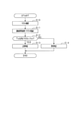
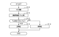
- step S10 the determination detection voltage VSb is acquired.
- step S11 a pseudo-abnormal processing is performed in which the logic of the voltage change signal Sg4 is set to H. As a result, the determination detection voltage VSb drops to 0V from the value acquired in step S10.
- step S12 it is determined whether or not the determination detection voltage VSb is less than the determination threshold value Vp within a predetermined time Tp after the logic of the voltage change signal Sg4 is switched to H.
- the predetermined time Tp is, for example, the detection detection voltage VSb for determination when the high voltage detection circuit 52, the second low-pass filter 62, the ASIC unit 63, the constant voltage source 64, and the first and second threshold resistors 65 and 66 are normal. It may be set to a sufficient time required for the voltage to drop to 0V.
- step S12 corresponds to the "voltage determination unit".
- step S12 If an affirmative decision is made in step S12, the logic of the second upper arm signal Sg2H is set to L, and the logic of the second and third lower arm signals Sg2L and Sg3L is set to H. As a result, the upper arm switch SWH is turned off and the lower arm switch SWL is turned on. When the upper arm switch SWH is turned off, the logic of the upper arm monitor signal SgmH is set to L, and when the lower arm switch SWL is turned on, the logic of the lower arm monitor signal SgmL is set to H. If an affirmative determination is made in step S12, the process proceeds to step S13, and it is determined that an abnormality that makes it impossible to determine an overvoltage abnormality has occurred. On the other hand, if a negative determination is made in step S12, the process proceeds to step S14, and it is determined that an abnormality that makes it impossible to determine an overvoltage abnormality has occurred.
- the determination detection voltage VSb was changed to 0V by performing the pseudo-abnormal processing. As a result, the determination detection voltage VSb is set to be less than the determination threshold value Vp, and the state in which the abnormality determination unit 67 determines that an overvoltage abnormality has occurred in the control system is simulated. At this time, if the determination detection voltage VSb is not less than the determination threshold value Vp, it can be determined that an abnormality that makes it impossible to determine an overvoltage abnormality has occurred.
- the determination detection voltage VSb determines the overvoltage abnormality of the control system. Therefore, even when the pseudo-abnormality processing is performed, the determination detection voltage VSb is used to determine whether or not an abnormality that makes it impossible to determine the overvoltage abnormality has occurred. As a result, the conditions can be met between the case where the overvoltage abnormality is determined and the case where the pseudo-abnormality processing is performed and the abnormality that makes it impossible to determine the overvoltage abnormality is determined. As a result, it is possible to suppress erroneous determination caused by the difference in the conditions for determining the abnormality that makes it impossible to determine the overvoltage abnormality.
- the determination detection voltage VSb is not less than the determination threshold value Vp within a predetermined time Tp after the pseudo-abnormality processing is performed, it is determined that an abnormality in which the overvoltage abnormality cannot be determined has occurred. It was configured. As a result, it is possible to accurately determine that an abnormality that makes it impossible to determine an overvoltage abnormality has occurred.
- the normal drive control When the normal drive control is executed, it is determined whether or not the normal drive control is normally executed. This makes it possible to determine that an abnormality has occurred in the configuration used for normal drive control. As a result, it is possible to suppress the occurrence of a situation in which the three-phase short-circuit control is not performed even though the three-phase short-circuit control should be performed due to an abnormality in the configuration used for the normal drive control.
- FIG. 8 shows the configuration of the control circuit 50 in this embodiment.
- the control circuit 50 includes a threshold power supply 81 which is a constant voltage power supply, a first threshold value switch 82, a second threshold value switch 83, and a fifth connection path L5.
- a threshold power supply 81 which is a constant voltage power supply
- a first threshold value switch 82 a resistor built-in transistor in which a base resistance and a base-emitter resistance are built in a PNP type bipolar transistor is used.
- the second threshold value switch 83 a resistor built-in transistor in which a base resistance and a base-emitter resistance are built in an NPN type bipolar transistor is used.
- the collector of the first threshold switch 82 is connected to the third intermediate point N3 provided in the third connection path L3, and the emitter of the first threshold switch 82 is connected to the threshold power supply 81.
- the collector of the second threshold switch 83 is connected to the base of the first threshold switch 82, and the emitter of the second threshold switch 83 is connected to the ground.
- the base of the second threshold switch 83 is connected to the microcomputer 51.
- the fifth connection path L5 connects the third intermediate point N3 of the third connection path L3 and the fourth intermediate point N4 between the ASIC unit 63 and the microcomputer 51.
- the determination threshold value Vp is input to the microcomputer 51 via the fifth connection path L5, and is input to the ASIC unit 63 via the third connection path L3.
- the determination threshold value Vp corresponds to the “threshold value”.
- the microcomputer 51 sets the logic of the threshold value change signal Sg5 to H when performing pseudo-abnormal processing.
- the threshold value change signal Sg5 is a signal output to the base of the second threshold value switch 83
- the logic H indicates an ON command of the second threshold value switch 83
- the logic L indicates the on command of the second threshold value switch 83.
- the second threshold switch 83 is turned on, the base of the first threshold switch 82 is connected to the ground.
- the first threshold switch 82 is turned on, and the voltage of the threshold power supply 81 is supplied.
- the voltage of the third connection path L3 rises, so that the determination threshold value Vp rises.
- the determination threshold value Vp rises to the upper limit voltage in the voltage range that can be input to the microcomputer 51.
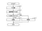
- step S11 the process of step S11 is performed, but in the process shown in FIG. 9, the process of step S15 is performed.
- step S15 the logic of the threshold value change signal Sg5 is set to H as a pseudo-abnormal processing.
- the determination threshold value Vp rises to the upper limit voltage in the voltage range that can be input to the microcomputer 51.
- the determination detection voltage VSb While the control system is starting up, the determination detection voltage VSb is set to an intermediate value in the voltage range that can be input to the microcomputer 51. Therefore, when the determination threshold value Vp rises to the upper limit voltage of the voltage range that can be input to the microcomputer 51, the determination detection voltage VSb is set to be less than the determination threshold value Vp. Therefore, also in this embodiment, when the pseudo-abnormality processing is performed, the state in which the abnormality determination unit 67 determines that an overvoltage abnormality has occurred in the control system is simulated. At this time, if the determination detection voltage VSb is not less than the determination threshold value Vp, it can be determined that an abnormality that makes it impossible to determine an overvoltage abnormality has occurred.
- the third embodiment will be described with reference to the drawings, focusing on the differences from the first embodiment.
- the pseudo-abnormal processing instead of the processing of reducing the detection detection voltage VSb for determination, a processing of increasing the terminal voltage VH of the smoothing capacitor 24 by controlling the output voltage of the DCDC converter 25 is performed.
- step S11 the process of step S11 is performed, but in the process shown in FIG. 10, the process of step S16 is performed.
- step S16 as a pseudo-abnormal processing, the target value of the output voltage of the DCDC converter 25 is increased so that the determination detection voltage VSb becomes less than the determination threshold value Vp. As a result, the terminal voltage VH of the smoothing capacitor 24 rises.
- a state in which the abnormality determination unit 67 determines that an overvoltage abnormality has occurred is simulated by performing pseudo-abnormal processing and setting the determination detection voltage VSb to be less than the determination threshold value Vp. Will be done. At this time, if the determination detection voltage VSb is not less than the determination threshold value Vp, it can be determined that an abnormality that makes it impossible to determine an overvoltage abnormality has occurred.
- the terminal voltage VH of the smoothing capacitor 24 was raised by boost control to raise the target value of the output voltage of the DCDC converter 25. Therefore, it is possible to check whether or not the configuration of the high voltage region (for example, the high voltage region side of the high voltage detection circuit 52) also operates normally by the pseudo-abnormal processing. As a result, even when an abnormality occurs in the configuration of the high voltage region, it can be determined that an abnormality that makes it impossible to determine an overvoltage abnormality has occurred.
- the fourth embodiment will be described with reference to the drawings, focusing on the differences from the first embodiment.
- the determination detection voltage VSb is less than the determination threshold value Vp by performing the pseudo-abnormal processing.
- the present embodiment it is determined whether or not the three-phase short circuit control is performed based on the driving states of the upper and lower arm switches SWH and SWL.
- step S17 it is determined whether or not the upper arm switch SWH is turned off based on the upper arm monitor signal SgmH. Further, it is determined whether or not the lower arm switch SWL is turned on based on the lower arm monitor signal SgmL.
- step S17 if an affirmative determination is made, the process proceeds to step S13, and if a negative determination is made, the process proceeds to step S14.
- step S17 corresponds to the "drive determination unit".
- the three-phase short-circuit control is not performed even though the pseudo-abnormal processing is performed and the state in which the overvoltage abnormality has occurred is simulated, an abnormality in which the overvoltage abnormality cannot be determined occurs. It can be determined that it has been done. As a result, it is possible to suppress the occurrence of a situation in which the three-phase short-circuit control is not implemented even though the three-phase short-circuit control should be implemented.
- the determination in step S12 is not limited to the microcomputer 51, but may be performed by the ASIC unit 63.
- the ASIC unit 63 includes a "voltage determination unit".
- the first connection path L1, the buffer circuit 60, and the first low-pass filter 61 may not be provided in the control circuit 50.
- the determination detection voltage VSb is input to the microcomputer 51 in the control circuit 50, and the microcomputer 51 may generate a switching command based on the determination detection voltage VSb.
- a processing that combines the processing described in the first to third embodiments may be performed.
- the determination detection voltage VSb may be set to be less than the determination threshold value Vp by increasing the determination threshold value Vp while reducing the determination detection voltage VSb.
- the high voltage detection circuit 52 is not limited to the one that converts so that the higher the terminal voltage VH of the smoothing capacitor 24 is, the lower the detection voltage VS is.
- the high-voltage detection circuit 52 may be converted so that the higher the terminal voltage VH of the smoothing capacitor 24 is, the higher the detection voltage VS is. In this case, if the determination detection voltage VSb is higher than the determination threshold value Vp, the abnormality determination unit 67 may determine that an abnormality has occurred in the control system.
- the determination detection voltage VSb and the determination threshold value Vp may be changed so that the determination detection voltage VSb is higher than the determination threshold value Vp.
- the determination detection voltage VSb may be increased to 5V.
- the determination threshold value Vp may be reduced to 0V.
- the microcomputer 51 may determine whether or not the determination detection voltage VSb is higher than the determination threshold value Vp within a predetermined time Tp after the pseudo-abnormal processing is performed.
- a control may be performed in which the upper arm switch SWH for three phases is turned on and the lower arm switch SWL for three phases is turned off.
- step S12 If it is determined that an overvoltage abnormality has occurred in the control system, only shutdown control may be implemented.
- the logic of the second upper and lower arm signals Sg2H and Sg2L is set to L in order to execute the shutdown control by the abnormality determination unit 67.
- the upper and lower arm switches SWH and SWL are turned off.
- the logic of the upper and lower arm monitor signals SgmH and SgmL is set to L.
- step S17 of the fourth embodiment it may be determined whether or not the upper arm switch SWH is turned off based on the upper arm monitor signal SgmH. Further, it may be determined whether or not the lower arm switch SWL is turned off based on the lower arm monitor signal SgmL.
- the switches SWH and SWL constituting the switching device unit 20 are not limited to IGBTs, and may be, for example, N-channel MOSFETs having a built-in body diode.
- the control amount of the rotary electric machine 10 is not limited to the torque, but may be, for example, the rotation speed of the rotor of the rotary electric machine 10.
- the rotary electric machine 10 is not limited to the permanent magnet synchronous machine, but may be, for example, a winding field type synchronous machine. Further, the rotary electric machine 10 is not limited to the synchronous machine, and may be, for example, an induction machine. Further, the rotary electric machine 10 is not limited to the one used as an in-vehicle main engine, but may be used for other purposes such as an electric power steering device and an electric motor constituting an electric compressor for air conditioning.
- the DCDC converter 25 does not have to be provided in the control system.
- the mobile body on which the control system is mounted is not limited to a vehicle, but may be, for example, an aircraft or a ship. Further, the mounting destination of the control system is not limited to the moving body.
- the controls and methods thereof described in the present disclosure are provided by a dedicated computer provided by configuring a processor and memory programmed to perform one or more functions embodied by a computer program. It may be realized. Alternatively, the controls and methods thereof described in the present disclosure may be implemented by a dedicated computer provided by configuring the processor with one or more dedicated hardware logic circuits. Alternatively, the control unit and method thereof described in the present disclosure may be a combination of a processor and memory programmed to perform one or more functions and a processor configured by one or more hardware logic circuits. It may be realized by one or more dedicated computers configured. Further, the computer program may be stored in a computer-readable non-transitional tangible recording medium as an instruction executed by the computer.
Landscapes
- Engineering & Computer Science (AREA)
- Power Engineering (AREA)
- Inverter Devices (AREA)
Applications Claiming Priority (2)
| Application Number | Priority Date | Filing Date | Title |
|---|---|---|---|
| JP2020-131692 | 2020-08-03 | ||
| JP2020131692A JP7276277B2 (ja) | 2020-08-03 | 2020-08-03 | 電力変換器の制御回路 |
Publications (1)
| Publication Number | Publication Date |
|---|---|
| WO2022030167A1 true WO2022030167A1 (ja) | 2022-02-10 |
Family
ID=80119752
Family Applications (1)
| Application Number | Title | Priority Date | Filing Date |
|---|---|---|---|
| PCT/JP2021/025575 Ceased WO2022030167A1 (ja) | 2020-08-03 | 2021-07-07 | 電力変換器の制御回路 |
Country Status (2)
| Country | Link |
|---|---|
| JP (1) | JP7276277B2 (enExample) |
| WO (1) | WO2022030167A1 (enExample) |
Citations (3)
| Publication number | Priority date | Publication date | Assignee | Title |
|---|---|---|---|---|
| JPH0546426A (ja) * | 1991-08-07 | 1993-02-26 | Toshiba Corp | 自己診断回路 |
| JP2019198139A (ja) * | 2018-05-07 | 2019-11-14 | 株式会社デンソー | 電力変換器の制御回路 |
| WO2020137907A1 (ja) * | 2018-12-26 | 2020-07-02 | 株式会社マキタ | 電動作業機 |
-
2020
- 2020-08-03 JP JP2020131692A patent/JP7276277B2/ja active Active
-
2021
- 2021-07-07 WO PCT/JP2021/025575 patent/WO2022030167A1/ja not_active Ceased
Patent Citations (3)
| Publication number | Priority date | Publication date | Assignee | Title |
|---|---|---|---|---|
| JPH0546426A (ja) * | 1991-08-07 | 1993-02-26 | Toshiba Corp | 自己診断回路 |
| JP2019198139A (ja) * | 2018-05-07 | 2019-11-14 | 株式会社デンソー | 電力変換器の制御回路 |
| WO2020137907A1 (ja) * | 2018-12-26 | 2020-07-02 | 株式会社マキタ | 電動作業機 |
Also Published As
| Publication number | Publication date |
|---|---|
| JP7276277B2 (ja) | 2023-05-18 |
| JP2022028347A (ja) | 2022-02-16 |
Similar Documents
| Publication | Publication Date | Title |
|---|---|---|
| US8264181B2 (en) | Controller for motor drive control system | |
| US9407181B2 (en) | Vehicle and method for controlling vehicle | |
| US9310440B2 (en) | Disconnection detecting device for rotating electrical machine, method for detecting disconnection of rotating electrical machine | |
| WO2009014245A1 (ja) | 半導体スイッチング素子の駆動制御装置 | |
| JP2015208143A (ja) | 電動機駆動装置 | |
| US10960919B2 (en) | Control device and electric power steering device using same | |
| WO2021161794A1 (ja) | 電力変換器の制御回路 | |
| JP6173516B1 (ja) | 電動機制御装置および電動機制御方法 | |
| US11368065B2 (en) | Controller of rotating electric machine | |
| JP6407382B1 (ja) | 電動機制御装置および電動機制御方法 | |
| JP2011019302A (ja) | モータ駆動システムの制御装置 | |
| CN110022116B (zh) | 电动机控制装置和电动机控制装置的控制方法 | |
| JP6983305B2 (ja) | 車両制御装置 | |
| JP6342043B1 (ja) | 電動機制御装置および電動機制御方法 | |
| WO2021161795A1 (ja) | 電力変換器の制御回路 | |
| JP4000866B2 (ja) | 駆動用電源装置及びフェール判定方法 | |
| WO2021161796A1 (ja) | 電力変換器の制御回路 | |
| JP7276277B2 (ja) | 電力変換器の制御回路 | |
| JP6203318B1 (ja) | 電動機制御装置および電動機制御方法 | |
| JP6708843B2 (ja) | 駆動装置 | |
| CN112953350B (zh) | 回转机械控制装置以及控制方法 | |
| CN117096832A (zh) | 功率转换装置 | |
| WO2022030190A1 (ja) | 電力変換器の制御回路 | |
| US20250105724A1 (en) | Power conversion device and drive device | |
| JP7631745B2 (ja) | インバータ制御装置、プログラム |
Legal Events
| Date | Code | Title | Description |
|---|---|---|---|
| 121 | Ep: the epo has been informed by wipo that ep was designated in this application |
Ref document number: 21854283 Country of ref document: EP Kind code of ref document: A1 |
|
| NENP | Non-entry into the national phase |
Ref country code: DE |
|
| 122 | Ep: pct application non-entry in european phase |
Ref document number: 21854283 Country of ref document: EP Kind code of ref document: A1 |