WO2022024560A1 - 回路基板及び電子機器 - Google Patents
回路基板及び電子機器 Download PDFInfo
- Publication number
- WO2022024560A1 WO2022024560A1 PCT/JP2021/022052 JP2021022052W WO2022024560A1 WO 2022024560 A1 WO2022024560 A1 WO 2022024560A1 JP 2021022052 W JP2021022052 W JP 2021022052W WO 2022024560 A1 WO2022024560 A1 WO 2022024560A1
- Authority
- WO
- WIPO (PCT)
- Prior art keywords
- conductor
- circuit board
- power supply
- signal
- end portion
- Prior art date
- Legal status (The legal status is an assumption and is not a legal conclusion. Google has not performed a legal analysis and makes no representation as to the accuracy of the status listed.)
- Ceased
Links
Images




Classifications
-
- H—ELECTRICITY
- H05—ELECTRIC TECHNIQUES NOT OTHERWISE PROVIDED FOR
- H05K—PRINTED CIRCUITS; CASINGS OR CONSTRUCTIONAL DETAILS OF ELECTRIC APPARATUS; MANUFACTURE OF ASSEMBLAGES OF ELECTRICAL COMPONENTS
- H05K1/00—Printed circuits
- H05K1/02—Details
- H05K1/0213—Electrical arrangements not otherwise provided for
- H05K1/0237—High frequency adaptations
-
- H—ELECTRICITY
- H01—ELECTRIC ELEMENTS
- H01P—WAVEGUIDES; RESONATORS, LINES, OR OTHER DEVICES OF THE WAVEGUIDE TYPE
- H01P3/00—Waveguides; Transmission lines of the waveguide type
- H01P3/02—Waveguides; Transmission lines of the waveguide type with two longitudinal conductors
- H01P3/08—Microstrips; Strip lines
- H01P3/085—Triplate lines
-
- H—ELECTRICITY
- H01—ELECTRIC ELEMENTS
- H01P—WAVEGUIDES; RESONATORS, LINES, OR OTHER DEVICES OF THE WAVEGUIDE TYPE
- H01P3/00—Waveguides; Transmission lines of the waveguide type
- H01P3/02—Waveguides; Transmission lines of the waveguide type with two longitudinal conductors
- H01P3/06—Coaxial lines
-
- H—ELECTRICITY
- H01—ELECTRIC ELEMENTS
- H01P—WAVEGUIDES; RESONATORS, LINES, OR OTHER DEVICES OF THE WAVEGUIDE TYPE
- H01P3/00—Waveguides; Transmission lines of the waveguide type
- H01P3/02—Waveguides; Transmission lines of the waveguide type with two longitudinal conductors
- H01P3/08—Microstrips; Strip lines
-
- H—ELECTRICITY
- H05—ELECTRIC TECHNIQUES NOT OTHERWISE PROVIDED FOR
- H05K—PRINTED CIRCUITS; CASINGS OR CONSTRUCTIONAL DETAILS OF ELECTRIC APPARATUS; MANUFACTURE OF ASSEMBLAGES OF ELECTRICAL COMPONENTS
- H05K1/00—Printed circuits
- H05K1/02—Details
- H05K1/0213—Electrical arrangements not otherwise provided for
- H05K1/0216—Reduction of cross-talk, noise or electromagnetic interference
- H05K1/0218—Reduction of cross-talk, noise or electromagnetic interference by printed shielding conductors, ground planes or power plane
- H05K1/0219—Printed shielding conductors for shielding around or between signal conductors, e.g. coplanar or coaxial printed shielding conductors
-
- H—ELECTRICITY
- H05—ELECTRIC TECHNIQUES NOT OTHERWISE PROVIDED FOR
- H05K—PRINTED CIRCUITS; CASINGS OR CONSTRUCTIONAL DETAILS OF ELECTRIC APPARATUS; MANUFACTURE OF ASSEMBLAGES OF ELECTRICAL COMPONENTS
- H05K1/00—Printed circuits
- H05K1/02—Details
- H05K1/03—Use of materials for the substrate
- H05K1/05—Insulated conductive substrates, e.g. insulated metal substrate
-
- H—ELECTRICITY
- H01—ELECTRIC ELEMENTS
- H01Q—ANTENNAS, i.e. RADIO AERIALS
- H01Q9/00—Electrically-short antennas having dimensions not more than twice the operating wavelength and consisting of conductive active radiating elements
- H01Q9/04—Resonant antennas
- H01Q9/0407—Substantially flat resonant element parallel to ground plane, e.g. patch antenna
-
- H—ELECTRICITY
- H05—ELECTRIC TECHNIQUES NOT OTHERWISE PROVIDED FOR
- H05K—PRINTED CIRCUITS; CASINGS OR CONSTRUCTIONAL DETAILS OF ELECTRIC APPARATUS; MANUFACTURE OF ASSEMBLAGES OF ELECTRICAL COMPONENTS
- H05K1/00—Printed circuits
- H05K1/02—Details
- H05K1/0213—Electrical arrangements not otherwise provided for
- H05K1/0216—Reduction of cross-talk, noise or electromagnetic interference
- H05K1/023—Reduction of cross-talk, noise or electromagnetic interference using auxiliary mounted passive components or auxiliary substances
- H05K1/0231—Capacitors or dielectric substances
-
- H—ELECTRICITY
- H05—ELECTRIC TECHNIQUES NOT OTHERWISE PROVIDED FOR
- H05K—PRINTED CIRCUITS; CASINGS OR CONSTRUCTIONAL DETAILS OF ELECTRIC APPARATUS; MANUFACTURE OF ASSEMBLAGES OF ELECTRICAL COMPONENTS
- H05K1/00—Printed circuits
- H05K1/02—Details
- H05K1/14—Structural association of two or more printed circuits
- H05K1/147—Structural association of two or more printed circuits at least one of the printed circuits being bent or folded, e.g. by using a flexible printed circuit
-
- H—ELECTRICITY
- H05—ELECTRIC TECHNIQUES NOT OTHERWISE PROVIDED FOR
- H05K—PRINTED CIRCUITS; CASINGS OR CONSTRUCTIONAL DETAILS OF ELECTRIC APPARATUS; MANUFACTURE OF ASSEMBLAGES OF ELECTRICAL COMPONENTS
- H05K2201/00—Indexing scheme relating to printed circuits covered by H05K1/00
- H05K2201/09—Shape and layout
- H05K2201/09209—Shape and layout details of conductors
-
- H—ELECTRICITY
- H05—ELECTRIC TECHNIQUES NOT OTHERWISE PROVIDED FOR
- H05K—PRINTED CIRCUITS; CASINGS OR CONSTRUCTIONAL DETAILS OF ELECTRIC APPARATUS; MANUFACTURE OF ASSEMBLAGES OF ELECTRICAL COMPONENTS
- H05K2201/00—Indexing scheme relating to printed circuits covered by H05K1/00
- H05K2201/09—Shape and layout
- H05K2201/09209—Shape and layout details of conductors
- H05K2201/0929—Conductive planes
- H05K2201/09336—Signal conductors in same plane as power plane
-
- H—ELECTRICITY
- H05—ELECTRIC TECHNIQUES NOT OTHERWISE PROVIDED FOR
- H05K—PRINTED CIRCUITS; CASINGS OR CONSTRUCTIONAL DETAILS OF ELECTRIC APPARATUS; MANUFACTURE OF ASSEMBLAGES OF ELECTRICAL COMPONENTS
- H05K2201/00—Indexing scheme relating to printed circuits covered by H05K1/00
- H05K2201/09—Shape and layout
- H05K2201/09209—Shape and layout details of conductors
- H05K2201/095—Conductive through-holes or vias
- H05K2201/09618—Via fence, i.e. one-dimensional array of vias
-
- H—ELECTRICITY
- H05—ELECTRIC TECHNIQUES NOT OTHERWISE PROVIDED FOR
- H05K—PRINTED CIRCUITS; CASINGS OR CONSTRUCTIONAL DETAILS OF ELECTRIC APPARATUS; MANUFACTURE OF ASSEMBLAGES OF ELECTRICAL COMPONENTS
- H05K2201/00—Indexing scheme relating to printed circuits covered by H05K1/00
- H05K2201/10—Details of components or other objects attached to or integrated in a printed circuit board
- H05K2201/10007—Types of components
- H05K2201/10015—Non-printed capacitor
Definitions
- the present invention relates to a circuit board and an electronic device including a signal conductor and a power supply conductor.
- the power transmission line described in Patent Document 1 As an invention relating to a conventional circuit board, for example, the power transmission line described in Patent Document 1 is known. As described in FIG. 13 of Patent Document 1, this power transmission line includes a signal conductor pattern, a power transmission conductor pattern, a first reference conductor, and a second reference conductor. The first reference conductor is placed on top of the signal conductor pattern. The second reference conductor is located below the signal conductor pattern. As a result, the signal conductor pattern, the first reference conductor and the second reference conductor have a stripline structure. The power transmission conductor pattern is arranged to the right of the signal conductor pattern. The power transfer conductor pattern is connected to the first reference conductor. As a result, the first reference conductor functions as a power supply line. As a result, in the power transmission line described in Patent Document 1, the insertion loss of the power supply line can be reduced.
- the power supply potential is connected to the first reference conductor. Therefore, noise may be mixed in the first reference conductor. In this case, noise may affect the high frequency signal transmitted through the signal conductor pattern.
- an object of the present invention is to provide a circuit board and an electronic device capable of suppressing the influence of noise on a high frequency signal transmitted to a signal conductor.
- the circuit board according to one embodiment of the present invention is With the board body A signal conductor provided on the main body of the substrate and to which a high frequency signal is transmitted, A power conductor provided on the substrate body and connected to the power potential, and a power conductor along at least a part of the signal conductor. A first reference conductor provided on the substrate body and insulated from the signal conductor and the power supply conductor. It is equipped with.
- the first member to the third member means a member or the like included in the signal transmission line. Unless otherwise specified, each part of the first member is defined as follows in the present specification.
- the front portion of the first member means the front half of the first member.
- the rear part of the first member means the rear half of the first member.
- the left portion of the first member means the left half of the first member.
- the right portion of the first member means the right half of the first member.
- the upper part of the first member means the upper half of the first member.
- the lower part of the first member means the lower half of the first member.
- the front end of the first member means the front end of the first member.
- the rear end of the first member means the rear end of the first member.
- the left end of the first member means the left end of the first member.
- the right end of the first member means the right end of the first member.
- the upper end of the first member means the upper end of the first member.
- the lower end of the first member means the lower end of the first member.
- the front end portion of the first member means the front end of the first member and its vicinity.
- the rear end portion of the first member means the rear end of the first member and its vicinity.
- the left end portion of the first member means the left end portion of the first member and its vicinity.
- the right end portion of the first member means the right end portion of the first member and its vicinity.
- the upper end portion of the first member means the upper end portion of the first member and its vicinity.
- the lower end portion of the first member means the lower end portion of the first member and its vicinity.
- circuit board according to the present invention it is possible to suppress the influence of noise on the high frequency signal transmitted to the signal conductor.
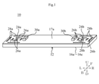
- FIG. 1 is an external perspective view of the circuit board 10.
- FIG. 2 is an exploded perspective view of the circuit board 10.
- FIG. 3 is an equivalent circuit diagram of the circuit board 10.
- FIG. 4 is an equivalent circuit diagram of the circuit board 10a.
- FIG. 5 is an equivalent circuit diagram of the circuit board 10b.
- FIG. 6 is a cross-sectional view of the circuit board 10c.
- FIG. 7 is an exploded perspective view of the circuit board 10d.
- FIG. 8 is a diagram showing the electronic device 1.
- FIG. 1 is an external perspective view of the circuit board 10.
- FIG. 2 is an exploded perspective view of the circuit board 10.
- FIG. 3 is an equivalent circuit diagram of the circuit board 10.
- the direction is defined as follows.
- the stacking direction of the board body 12 of the circuit board 10 is defined as the vertical direction of the circuit board.
- the longitudinal direction of the circuit board 10 is defined as the left-right direction of the circuit board.
- the lateral direction of the circuit board 10 is defined as the front-rear direction of the circuit board.
- the vertical direction of the circuit board, the front-rear direction of the circuit board, and the left-right direction of the circuit board are orthogonal to each other.
- the vertical direction of the circuit board, the front-rear direction of the circuit board, and the left-right direction of the circuit board do not have to coincide with the vertical direction, the left-right direction, and the front-back direction of the circuit board 10 in actual use.
- the circuit board 10 is used for connecting two circuits in an electronic device such as a mobile phone. As shown in FIGS. 1 and 2, the circuit board 10 includes a substrate main body 12, a signal conductor 18, a first power conductor 20a, a second power conductor 20b, a third power conductor 20c, a first reference conductor 22a, and a second reference. Conductor 22b, 1st signal electrode 24a, 2nd signal electrode 24b, 1st reference electrode 26a (see FIG. 1), 2nd reference electrode 26b (see FIG. 1), 1st power supply electrode 28a (see FIG. 1), 2nd Power supply electrode 28b (see FIG.
- first chip capacitor 30a first chip capacitor 30b, second chip capacitor 30b, reference electrodes 222a, 222b, power supply electrodes 224a, 224b, first interlayer connection conductor v1, second interlayer connection conductor v2, and a plurality of first layers. It includes a three-layer connection conductor v3 and a plurality of fourth interlayer connection conductors v4.
- reference numerals are given to typical interlayer connection conductors among the plurality of third interlayer connection conductors v3 and the plurality of fourth interlayer connection conductors v4.
- the substrate main body 12 has a plate shape. As shown in FIGS. 1 and 2, the substrate main body 12 has a rectangular shape having a long side extending in the front-rear direction of the circuit board when viewed in the vertical direction of the circuit board. The substrate body 12 has flexibility. Therefore, the substrate main body 12 can be used in a folded state in an electronic device.
- the substrate main body 12 has a structure in which a resist layer 17a and insulating resin layers 16a to 16c (a plurality of insulator layers) are laminated in the vertical direction of the circuit board.
- the resist layer 17a and the insulating resin layers 16a to 16c are laminated so as to be arranged in this order from top to bottom in the vertical direction of the circuit board.
- the insulating resin layers 16a to 16c are flexible dielectric sheets.
- the material of the insulating resin layers 16a to 16c is a thermoplastic resin such as polyimide or a liquid crystal polymer.
- the insulating resin layers 16a to 16c have the same rectangular shape as the substrate main body 12 when viewed in the vertical direction of the circuit board.
- the resist layer 17a will be described later.
- the signal conductor 18 is provided on the substrate main body 12. More specifically, the signal conductor 18 is provided on the upper main surface of the insulating resin layer 16b. As a result, the signal conductor 18 is provided in the substrate main body 12.
- the signal conductor 18 is a conductor layer having a linear shape extending in the left-right direction of the circuit board.
- the signal conductor 18 is arranged at the center of the upper main surface of the insulating resin layer 16b in the front-rear direction of the circuit board.
- the left end of the signal conductor 18 is located at the left end of the insulating resin layer 16b.
- the right end of the signal conductor 18 is located at the right end of the insulating resin layer 16c.
- a high frequency signal is transmitted to the signal conductor 18.
- the first power supply conductor 20a is provided on the substrate main body 12.
- the first power supply conductor 20a is arranged above the signal conductor 18 in the vertical direction of the circuit board so as to overlap the signal conductor 18 when viewed in the vertical direction of the circuit board.
- “the first power conductor 20a is arranged above the signal conductor 18 in the vertical direction of the circuit board” refers to the following state. At least a part of the first power supply conductor 20a is arranged in a region through which the signal conductor 18 is translated when moving in parallel on the circuit board.
- the first power supply conductor 20a may be contained in the region through which the signal conductor 18 is translated when the signal conductor 18 is translated in the upward direction of the circuit board, or is passed when the signal conductor 18 is translated in the upward direction of the circuit board. It may protrude from the area to be used. In the present embodiment, the first power supply conductor 20a protrudes from the region through which the signal conductor 18 passes when translated in the upward direction of the circuit board.
- the first power supply conductor 20a is provided on the upper main surface of the insulating resin layer 16a. As shown in FIG. 3, the first power supply conductor 20a is a conductor layer having a rectangular shape having a long side extending in the left-right direction of the circuit board when viewed in the vertical direction of the circuit board. The first power supply conductor 20a has a shape that substantially matches the substrate main body 12 when viewed in the vertical direction of the circuit board. However, the first power supply conductor 20a is slightly smaller than the substrate main body 12 when viewed in the vertical direction of the circuit board.
- the first power supply conductor 20a overlaps with the signal conductor 18 when viewed in the vertical direction of the circuit board.
- the first power supply conductor 20a is along at least a part of the section of the signal conductor 18. More specifically, the first power supply conductor 20a overlaps with at least a part of the signal conductor 18 when viewed in the vertical direction of the circuit board (the stacking direction of the substrate main body).
- the first power supply conductor 20a overlaps with a section excluding the left end portion and the right end portion of the signal conductor 18 when viewed in the vertical direction of the circuit board.
- the first power supply conductor 20a extends in the left-right direction of the circuit board along the signal conductor 18 in the section excluding the left end portion and the right end portion of the signal conductor 18. As a result, the first power supply conductor 20a is close to the section excluding the left end portion and the right end portion of the signal conductor 18.
- the third power conductor 20c is provided on the substrate main body 12.
- the third power supply conductor 20c is arranged below the signal conductor 18 in the vertical direction of the circuit board so as to overlap the signal conductor 18 when viewed in the vertical direction of the circuit board.
- the third power conductor 20c is provided on the upper main surface of the insulating resin layer 16c.
- the third power supply conductor 20c is a conductor layer having a rectangular shape having a long side extending in the left-right direction of the circuit board when viewed in the vertical direction of the circuit board.
- the third power supply conductor 20c has a shape that substantially matches the substrate main body 12 when viewed in the vertical direction of the circuit board. However, the third power supply conductor 20c is slightly smaller than the substrate main body 12 when viewed in the vertical direction of the circuit board.
- the third power supply conductor 20c overlaps with the signal conductor 18 when viewed in the vertical direction of the circuit board.
- the third power conductor 20c is along at least a part of the signal conductor 18. More specifically, the third power supply conductor 20c overlaps with at least a part of the signal conductor 18 when viewed in the vertical direction of the circuit board (the stacking direction of the substrate main body).
- the third power supply conductor 20c overlaps with the section excluding the left end portion and the right end portion of the signal conductor 18 when viewed in the vertical direction of the circuit board.
- the third power supply conductor 20c extends in the left-right direction of the circuit board along the signal conductor 18 in the section excluding the left end portion and the right end portion of the signal conductor 18. As a result, the third power supply conductor 20c is close to the section excluding the left end portion and the right end portion of the signal conductor 18.
- the second power conductor 20b is provided on the substrate main body 12.
- the second power supply conductor 20b is arranged at the same position as the signal conductor 18 in the vertical direction of the circuit board.
- the second power conductor 20b is provided on the upper main surface of the insulating resin layer 16b.
- the second power supply conductor 20b is a conductor layer having a rectangular shape having a long side extending in the front-rear direction of the circuit board when viewed in the vertical direction of the circuit board.
- the second power supply conductor 20b has a shape that substantially matches the substrate main body 12 when viewed in the vertical direction of the circuit board. However, the second power supply conductor 20b is slightly smaller than the substrate main body 12 when viewed in the vertical direction of the circuit board.
- the second power supply conductor 20b is along at least a part of the section of the signal conductor 18.
- the second power conductor 20b is along the entire signal conductor 18. More specifically, the second power conductor 20b is not provided around the signal conductor 18 so that the second power conductor 20b is insulated from the signal conductor 18. As a result, the signal conductor 18 is surrounded by the second power supply conductor 20b when viewed in the vertical direction of the circuit board. Therefore, the second power supply conductor 20b is along the entire signal conductor 18. As a result, the second power supply conductor 20b is in close proximity to the entire signal conductor 18.
- the first power supply conductor 20a, the second power supply conductor 20b, and the third power supply conductor 20c as described above are connected to the power supply potential.
- the power supply potential is, for example, 1.8 V, 3 V, or the like.
- the first reference conductor 22a is provided on the substrate main body 12.
- the first reference conductor 22a is provided at the left end portion of the upper main surface of the insulating resin layer 16a.
- the signal conductor 18 is provided on the upper main surface of the insulating resin layer 16b. Therefore, the first reference conductor 22a is insulated from the signal conductor 18.
- the first reference conductor 22a is a conductor layer having a rectangular shape when viewed in the vertical direction of the circuit board. However, the first reference conductor 22a has a protruding portion 122a that protrudes from the right side of the rectangle to the right side of the circuit board when viewed in the vertical direction of the circuit board.
- the first reference conductor 22a is insulated from the first power supply conductor 20a. Therefore, the first power supply conductor 20a is not provided around the first reference conductor 22a. As a result, the first reference conductor 22a is surrounded by the first power supply conductor 20a when viewed in the vertical direction of the circuit board. However, the first reference conductor 22a is not in contact with the first power supply conductor 20a.
- the second reference conductor 22b has a structure symmetrical to that of the first reference conductor 22a. Therefore, the description of the second reference conductor 22b will be omitted.
- the first reference conductor 22a and the second reference conductor 22b as described above are connected to the reference potential.
- the reference potential is, for example, the ground potential (ie, 0V).
- the first reference conductor 22a and the second reference conductor 22b are ground conductors.
- the first signal electrode 24a is used for connection with an external circuit.
- the first signal electrode 24a is provided at the left end portion of the upper main surface of the insulating resin layer 16a.
- the first signal electrode 24a overlaps with the left end portion of the signal conductor 18 when viewed in the vertical direction of the circuit board.
- the first signal electrode 24a has a rectangular shape when viewed in the vertical direction of the circuit board.
- the first reference conductor 22a is not provided around the first signal electrode 24a so that the first signal electrode 24a is insulated from the first reference conductor 22a.
- the first interlayer connection conductor v1 is provided at the left end portion of the insulating resin layer 16a.
- the first interlayer connection conductor v1 penetrates the insulating resin layer 16a in the vertical direction.
- the upper end of the first interlayer connection conductor v1 is connected to the first signal electrode 24a.
- the lower end of the first interlayer connection conductor v1 is connected to the left end portion of the signal conductor 18.
- the first interlayer connection conductor v1 connects the signal conductor 18 and the first signal electrode 24a. That is, the first signal electrode 24a is connected to the left end portion (first end portion) of the signal conductor 18.
- the first interlayer connection conductor v1 is, for example, a via hole conductor.
- the via hole conductor is formed by filling a through hole penetrating the insulating resin layer 16a in the vertical direction with a conductive paste and sintering the conductive paste.
- the high frequency signal is input / output to / from the signal conductor 18 via the first signal electrode 24a.
- the second signal electrode 24b and the second interlayer connection conductor v2 have a symmetrical structure with the first signal electrode 24a and the first interlayer connection conductor v1. Therefore, the description of the second signal electrode 24b and the second interlayer connection conductor v2 will be omitted.
- the resist layer 17a is a flexible and insulating protective layer.
- the resist layer 17a covers the entire surface of the upper main surface of the insulating resin layer 16a. As a result, the resist layer 17a protects the first power supply conductor 20a, the first reference conductor 22a, and the second reference conductor 22b.
- the resist layer 17a is provided with openings h1 to h10.
- the opening h1 overlaps with the first signal electrode 24a when viewed in the vertical direction of the circuit board.
- the first signal electrode 24a is exposed to the outside from the circuit board 10 through the opening h1.
- the opening h2 is provided in front of the opening h1 in the front-rear direction of the circuit board.
- the opening h3 is provided on the right side of the opening h1 in the left-right direction of the circuit board.
- the opening h4 is provided behind the opening h1 in the front-rear direction of the circuit board.
- the opening h5 is provided on the left side of the opening h1 in the left-right direction of the circuit board.
- the opening h6 is provided in front of the opening h2 in the front-rear direction of the circuit board.
- the opening h7 is provided behind the opening h4 in the front-rear direction of the circuit board.
- the opening h8 is provided on the left side of the opening h5 in the left-right direction of the circuit board.
- the opening h9 is provided on the right side of the opening h3 in the left-right direction of the circuit board.
- the protruding portion 122a of the first reference conductor 22a is exposed to the outside through the opening h9.
- the portion of the protruding portion 122a of the first reference conductor 22a exposed from the opening h9 is the reference electrode 222a.
- the reference electrode 222a is connected to the first reference conductor 22a.
- the opening h10 is provided on the right side of the opening h3 in the left-right direction of the circuit board.
- the opening h10 is provided in front of the opening h9 in the front-rear direction of the circuit board.
- the first power conductor 20a is exposed to the outside through the opening h10.
- the portion of the first power conductor 20a exposed from the opening h9 is the power electrode 224a.
- the power supply electrode 224a is connected to the first power supply conductor 20a.
- the openings h11 to h20, the second reference electrode 26b, the second power supply electrode 28b, the reference electrode 222b and the power supply electrode 224b are the openings h1 to h10, the first reference electrode 26a, the first power supply electrode 28a, the reference electrode 222a and the power supply. It has a structure symmetrical to the electrode 224a. Therefore, the description of the openings h11 to h20, the second reference electrode 26b, the second power supply electrode 28b, the reference electrode 222b, and the power supply electrode 224b will be omitted.
- the signal conductor 18, the first power conductor 20a, the second power conductor 20b, the third power conductor 20c, the first reference conductor 22a, the second reference conductor 22b, the first signal electrode 24a and the second signal electrode 24b as described above are For example, it is formed by etching the copper foil provided on the upper main surface or the lower main surface of the insulating resin layers 16a to 16c.
- the plurality of third interlayer connection conductors v3 are provided on the substrate main body 12 so as to be located in front of the signal conductor 18 in the front-rear direction of the circuit board.
- the plurality of third interlayer connection conductors v3 are arranged so as to be arranged in a line at equal intervals in the left-right direction of the circuit board.
- the plurality of third interlayer connection conductors v3 penetrate the insulating resin layers 16a and 16b in the vertical direction of the circuit board.
- the upper ends of the plurality of third interlayer connection conductors v3 are connected to the first power supply conductor 20a.
- the intermediate portion of the plurality of third interlayer connection conductors v3 is connected to the second power supply conductor 20b.
- the lower ends of the plurality of third interlayer connection conductors v3 are connected to the third power supply conductor 20c.
- the plurality of third interlayer connection conductors v3 connect the first power supply conductor 20a, the second power supply conductor 20b, and the third power supply conductor 20c.
- the plurality of fourth interlayer connection conductors v4 are provided on the substrate main body 12 so as to be located behind the signal conductor 18 in the front-rear direction of the circuit board.
- the plurality of fourth interlayer connection conductors v4 are arranged so as to be arranged in a line at equal intervals in the left-right direction of the circuit board.
- the plurality of fourth interlayer connection conductors v4 penetrate the insulating resin layers 16a and 16b in the vertical direction of the circuit board.
- the upper ends of the plurality of fourth interlayer connection conductors v4 are connected to the first power supply conductor 20a.
- the intermediate portion of the plurality of fourth interlayer connection conductors v4 is connected to the second power supply conductor 20b.
- the lower ends of the plurality of fourth interlayer connection conductors v4 are connected to the third power supply conductor 20c.
- the plurality of fourth interlayer connection conductors v4 connect the first power supply conductor 20a, the second power supply conductor 20b, and the third power supply conductor 20c.
- the plurality of third interlayer connecting conductors v3 and the plurality of fourth interlayer connecting conductors v4 are, for example, via hole conductors.
- the via hole conductor is formed by filling the through holes penetrating the insulating resin layers 16a and 16b in the vertical direction with the conductive paste and sintering the conductive paste.
- the first reference conductor 22a is connected to the first power supply conductor 20a via the first capacitance C1.
- the first chip capacitor 30a of FIGS. 1 and 2 has a first capacitance C1. More specifically, as shown in FIG. 2, the first chip capacitor 30a is mounted on the reference electrode 222a and the power supply electrode 224a by soldering. Therefore, the first capacitor electrode of the first chip capacitor 30a is connected to the first reference conductor 22a. The second capacitor electrode of the first chip capacitor 30a is connected to the first power supply conductor 20a.
- the signal conductor 18 has a left end portion (first end portion), a right end portion (second end portion), and a center point C.
- the center point C is located at the center of the left end portion (first end portion) and the right end portion (second end portion) in the path formed by the signal conductor 18.
- the reference electrode 222a and the power supply electrode 224a are arranged closer to the left end portion (first end portion) of the signal conductor 18 than the center point C of the signal conductor 18.
- the reference electrode 222a and the power supply electrode 224a are arranged in the vicinity of the left end portion of the signal conductor 18.
- the first chip capacitor 30a is mounted on the reference electrode 222a and the power supply electrode 224a. Therefore, the first reference conductor 22a is connected to the first power supply conductor 20a via the first capacitance C1 near the left end portion (first end portion) of the signal conductor 18 from the center point C of the signal conductor 18. .. In the present embodiment, the first reference conductor 22a is connected to the first power supply conductor 20a via the first capacitance C1 in the vicinity of the left end portion (first end portion) of the signal conductor 18.
- the second reference conductor 22b is connected to the first power supply conductor 20a via the second capacitance C2.
- the second chip capacitor 30b in FIGS. 1 and 2 has a second capacitance C2. More specifically, as shown in FIG. 2, the second chip capacitor 30b is mounted on the reference electrode 222b and the power supply electrode 224b by soldering. Therefore, the first capacitor electrode of the second chip capacitor 30b is connected to the second reference conductor 22b. The second capacitor electrode of the second chip capacitor 30b is connected to the first power supply conductor 20a.
- the reference electrode 222b and the power supply electrode 224b are arranged near the right end portion (second end portion) of the signal conductor 18 from the center point C of the signal conductor 18.
- the reference electrode 222b and the power supply electrode 224b are arranged near the right end portion of the signal conductor 18.
- the second chip capacitor 30b is mounted on the reference electrode 222b and the power supply electrode 224b. Therefore, the second reference conductor 22b is connected to the first power supply conductor 20a via the second capacitance C2 near the right end portion (first end portion) of the signal conductor 18 from the center point C of the signal conductor 18. .. In the present embodiment, the second reference conductor 22b is connected to the first power supply conductor 20a via the second capacitance C2 in the vicinity of the right end portion (second end portion) of the signal conductor 18.
- the circuit board 10 can function as a high frequency signal transmission line. More specifically, when the high frequency signal is transmitted through the signal conductor 18, the return current flows through the first power supply conductor 20a. This return current is preferably guided to a reference potential. Therefore, in the circuit board 10, the first reference conductor 22a is insulated from the signal conductor 18 and the first power supply conductor 20a. As a result, when the first reference conductor 22a is connected to the first power supply conductor 20a via the first capacitance C1, the return current is changed from the first power supply conductor 20a to the first capacitance C1, the first reference conductor 22a and the first. It flows to the ground potential via the reference electrode 26a. As a result, the circuit board 10 can function as a high-frequency signal transmission line.
- a strip line is composed of a signal conductor and two reference conductors.
- Such circuit boards may further include power conductors.
- it may be difficult to secure a space for providing a power supply conductor having a large area. As a result, the resistance value of the power supply conductor becomes large.
- the first power supply conductor 20a is along at least a part of the signal conductor 18.
- a high frequency signal transmission line through which a high frequency signal is transmitted is formed by utilizing the capacitance formed between the first power supply conductor 20a and the signal conductor 18. Therefore, in the circuit board 10, the area of the first reference conductor 22a and the second reference conductor 22b can be reduced, and the area of the first power supply conductor 20a can be increased. As a result, the increase in size of the circuit board 10 is suppressed. Further, since the area of the first power supply conductor 20a becomes large, the resistance value of the first power supply conductor 20a becomes low. Therefore, when the high frequency signal is transmitted through the signal conductor 18, the return current tends to flow through the first power supply conductor 20a. As a result, the insertion loss of the circuit board 10 can be reduced.
- the circuit board 10 it is possible to suppress the influence of noise on the high frequency signal transmitted to the signal conductor 18. More specifically, in the circuit board 10, the capacitance formed between the first power supply conductor 20a and the signal conductor 18 is used to form a high frequency signal transmission line through which a high frequency signal is transmitted. In this case, noise mixed in the circuit board 10 from the first power supply electrode 28a and the second power supply electrode 28b may affect the high frequency signal transmitted through the signal conductor 18.
- the first reference conductor 22a is insulated from the signal conductor 18 and the first power supply conductor 20a.
- the noise mixed in the circuit board 10 from the first power supply electrode 28a and the second power supply electrode 28b is the first. 1 Flows to the reference potential via the power conductor 20a, the first capacitance C1 and the first reference electrode 26a. As a result, it is possible to suppress the influence of noise on the high frequency signal transmitted through the signal conductor 18.
- the insertion loss of the circuit board 10 can be further reduced. More specifically, the first reference conductor 22a is connected to the first power supply conductor 20a via the first capacitance C1 near the left end portion (first end portion) of the signal conductor 18 from the center point C of the signal conductor 18. Has been done. As a result, the portion where the first reference conductor 22a and the first power supply conductor 20a are connected via the first capacitance C1 is separated from the center point C of the signal conductor 18. Therefore, the section where the signal conductor 18 is along the first power supply conductor 20a becomes long. In the high frequency signal transmission line, the section in which the first power supply conductor 20a having a low resistance value is used becomes long. As a result, according to the circuit board 10, the insertion loss of the circuit board 10 can be further reduced.
- the insertion loss of the circuit board 10 can be further reduced. More specifically, the second reference conductor 22b is connected to the first power supply conductor 20a via the second capacitance C2 near the right end portion (second end portion) of the signal conductor 18 from the center point C of the signal conductor 18. Has been done. As a result, the portion where the second reference conductor 22b and the first power supply conductor 20a are connected via the second capacitance C2 is separated from the center point C of the signal conductor 18. Therefore, the section in which the signal conductor 18 is along the first power supply conductor 20a becomes long. In the high frequency signal transmission line, the section in which the first power supply conductor 20a having a low resistance value is used becomes long. As a result, according to the circuit board 10, the insertion loss of the circuit board 10 can be further reduced.
- the circuit board 10 can be downsized. More specifically, the first chip capacitor 30a is the first capacitance C1. The first chip capacitor 30a can easily obtain a large capacitance value. Therefore, the circuit board 10 is made smaller than the circuit board in which the chip capacitor is not used to obtain the first capacitance C1.
- FIG. 4 is an equivalent circuit diagram of the circuit board 10a.
- the circuit board 10a is different from the circuit board 10 in that the first high-pass filter HPF1 and the second high-pass filter HPF2 are provided in place of the first capacitance C1 and the second capacitance C2. This point will be described below.
- the first reference conductor 22a is connected to the first power supply conductor 20a via the first high-pass filter HPF1.
- the first high-pass filter HPF1 includes a third capacitance C3 and an inductor L1.
- the third capacitance C3 is connected to the first power supply conductor 20a and the first reference conductor 22a, similarly to the first capacitance C1.
- the inductor L1 is connected to the first power supply conductor 20a and the first power supply electrode 28a.
- the pass band of the first high-pass filter HPF1 includes the frequency of the high frequency signal transmitted through the signal conductor 18.
- the return current has the same frequency as the high frequency signal transmitted through the signal conductor 18. Therefore, the return current can pass between the first power supply conductor 20a and the first reference conductor 22a. Further, the noise can pass between the first power supply conductor 20a and the first reference conductor 22a.
- the inductor L1 may be a chip inductor or wiring in the circuit board 10a.
- the second reference conductor 22b is connected to the first power supply conductor 20a via the second high-pass filter HPF2.
- the second high-pass filter HPF2 includes a fourth capacitance C4 and an inductor L2.
- the fourth capacitance C4 is connected to the first power supply conductor 20a and the second reference conductor 22b, similarly to the second capacitance C2.
- the inductor L2 is connected to the first power supply conductor 20a and the second power supply electrode 28b.
- the pass band of the second high-pass filter HPF2 includes the frequency of the high frequency signal transmitted through the signal conductor 18.
- the return current has the same frequency as the high frequency signal transmitted through the signal conductor 18. Therefore, the return current can pass between the first power supply conductor 20a and the second reference conductor 22b.
- the inductor L2 may be a chip inductor or wiring in the circuit board 10a. Since the other structures of the circuit board 10a are the same as those of the circuit board 10, the description thereof will be omitted.
- the inductor L1 is used in the circuit board 10a.
- a desired pass band can be obtained by the first high-pass filter HPF1 provided with the third capacitance C3 and the inductor L1.
- the desired pass band can be obtained by the second high-pass filter HPF2.
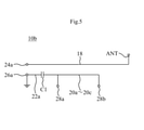
- FIG. 5 is an equivalent circuit diagram of the circuit board 10b.
- the circuit board 10b is different from the circuit board 10 in that it is provided with an antenna ANT instead of the second capacitance C2, the second reference conductor 22b, and the second reference electrode 26b. This point will be described below.
- the circuit board 10b further includes an antenna ANT.
- the right end of the signal conductor 18 is connected to an antenna ANT for transmitting and / or receiving a high frequency signal.
- the antenna ANT is formed, for example, by the conductor layer of the circuit board 10b. In this case, the antenna ANT is a part of the circuit board 10b. However, the antenna ANT does not have to be a part of the circuit board 10b. Therefore, the circuit board 10b is connected to the antenna ANT or an integrated circuit including the antenna ANT.
- the circuit board 10b When the signal conductor 18 is connected to the antenna ANT, the circuit board 10b does not need to transmit the reference potential connected to the first reference electrode 26a to the subsequent circuit board. Therefore, the circuit board 10b does not include the second capacitance C2, the second reference conductor 22b, and the second reference electrode 26b. Since the other structures of the circuit board 10b are the same as those of the circuit board 10, the description thereof will be omitted.
- FIG. 6 is a cross-sectional view of the circuit board 10c.
- FIG. 6 shows a cross section orthogonal to the left-right direction.
- the circuit board 10c further includes power supply conductors 20d to 20g, reference conductors 22c to 22e, and interlayer connection conductors v5 to v8, and the substrate body 12 further includes a resist layer 17b. Is different from. The differences between them will be described below.
- the power supply conductor 20d, the reference conductor 22c, the power supply conductor 20e, the reference conductor 22d, the power supply conductor 20f, the reference conductor 22e, and the power supply conductor 20g are arranged in this order from the back to the front in the front-rear direction of the circuit board.
- the power supply conductors 20d to 20g and the reference conductors 22c to 22e extend in the front-rear direction of the circuit board.
- Such reference conductors 22c to 22e are connected to the third power supply conductor 20c via the first capacitance C1 and are insulated from the signal conductor 18.
- the interlayer connection conductor v5 connects the third power supply conductor 20c and the power supply conductor 20d.
- the interlayer connection conductor v6 connects the third power supply conductor 20c and the power supply conductor 20e.
- the interlayer connection conductor v7 connects the third power supply conductor 20c and the power supply conductor 20f.
- the interlayer connection conductor v8 connects the third power supply conductor 20c and the power supply conductor 20g.
- the resist layer 17b is a flexible and insulating protective layer.
- the resist layer 17b covers the entire lower main surface of the insulating resin layer 16c. As a result, the resist layer 17b protects the power supply conductors 20d to 20g and the reference conductors 22c to 22e.
- the resist layer 17b is provided with an opening.
- the opening overlaps with the reference conductors 22c to 22e when viewed in the vertical direction of the circuit board.
- the reference conductors 22c to 22e are exposed to the outside from the circuit board 10c through the openings.
- the gold-plated layers 50c to 50e are provided on the reference conductors 22c to 22e.
- the circuit board 10c as described above is fixed to the metal housing 200 connected to the reference potential.
- the gold-plated layers 50c to 50e are connected to the metal housing 200. Therefore, the reference conductors 22c to 22e are connected to the reference potential.
- Each of the reference conductors 22c to 22e may be connected to the metal housing 200 at a plurality of places. That is, the circuit board 10 may have the structure of the cross section of FIG. 6 at a plurality of places. Since the other structures of the circuit board 10c are the same as those of the circuit board 10, the description thereof will be omitted.
- the circuit board 10c it is possible to suppress the influence of noise on the high frequency signal transmitted through the signal conductor 18. More specifically, the reference conductors 22c to 22e are capacitively coupled to the third power supply conductor 20c. Therefore, noise flows from the third power supply conductor 20c to the reference conductors 22c to 22e. Then, the noise flows to the metal housing 200 via the gold-plated layers 50c to 50e. As a result, according to the circuit board 10c, it is possible to suppress the influence of noise on the high frequency signal transmitted through the signal conductor 18. Further, by connecting each of the reference conductors 22c to 22e to the metal housing 200 at a plurality of places, it is possible to further suppress the influence of noise on the high frequency signal transmitted through the signal conductor 18. In the circuit board 10c, the gold-plated layers 50c to 50e and the metal housing 200 may be bonded by a conductive bonding material such as solder.
- FIG. 7 is an exploded perspective view of the circuit board 10d.
- the circuit board 10d is different from the circuit board 10 in that it does not include the first chip capacitor 30a and the second chip capacitor 30b.
- the first capacitance C1 is a capacitance formed between the first reference conductor 22a and the second power supply conductor 20b.
- the second capacitance C2 is a capacitance formed between the second reference conductor 22b and the second power supply conductor 20b. Since the other structures of the circuit board 10d are the same as those of the circuit board 10, the description thereof will be omitted.
- the circuit board 10d the first capacitance C1 and the second capacitance C2 are formed by the capacitance. Therefore, the circuit board 10d does not require a chip capacitor. Further, the mounting process of the chip capacitor becomes unnecessary at the time of manufacturing the circuit board 10d. As a result, the manufacturing cost of the circuit board 10d is reduced.
- FIG. 8 is a diagram showing the electronic device 1.
- the first chip capacitor 30a and the second chip capacitor 30b are omitted.
- the electronic device 1 is, for example, a portable wireless communication terminal such as a smartphone.
- the electronic device 1 includes a circuit board 10 and circuit boards 300 and 302.
- the left end portion of the circuit board 10 is connected to the circuit board 300. More specifically, the first signal electrode 24a, the first reference electrode 26a, and the first power supply electrode 28a are fixed to the electrodes of the circuit board 300 by soldering.
- the right end portion of the circuit board 10 is connected to the circuit board 302. More specifically, the second signal electrode 24b, the second reference electrode 26b, and the second power supply electrode 28b are fixed to the electrodes of the circuit board 302 by soldering. As a result, a high frequency signal is transmitted to the signal conductor 18.
- the first power supply conductor 20a, the second power supply conductor 20b, and the third power supply conductor 20c are connected to the power supply potential.
- the first reference conductor 22a and the second reference conductor 22b are connected to the reference potential.
- the vertical position of the circuit board 300 and the vertical position of the circuit board 302 are different. Therefore, the circuit board 10 is bent. Since the material of the insulating resin layers 16a to 16c is a thermoplastic resin, the circuit board 10 can be bent.
- the circuit board 10 may be connected to the circuit board 300 and the circuit board 302 via a connector. Further, the electronic device 1 may include any of the circuit boards 10a to 10d instead of the circuit board 10.
- the signal transmission line according to the present invention is not limited to the circuit boards 10, 10a to 10d, and can be changed within the scope of the gist thereof. Further, it is possible to combine the configurations of the circuit boards 10, 10a to 10d.
- the signal conductor 18 extends linearly in the left-right direction of the circuit board. However, the signal conductor 18 may be bent when viewed in the vertical direction of the circuit board.
- the circuit boards 10, 10a to 10d may be provided with any one of the first power supply conductor 20a, the second power supply conductor 20b, and the third power supply conductor 20c.
- the first reference conductor 22a is connected to any one of the first power supply conductor 20a, the second power supply conductor 20b, and the third power supply conductor 20c via the first capacitance C1 and is insulated from the signal conductor 18. You just have to.
- the first power supply conductor 20a and / or the third power supply conductor 20c may be along the entire signal conductor 18.
- the first reference conductor 22a is the first power conductor 20a and the first power conductor 20a near the center point C of the signal conductor 18 from the left end portion (first end portion) of the signal conductor 18. It may be connected via the capacitance C1.
- the second reference conductor 22b is located near the center point C of the signal conductor 18 from the right end (second end) of the signal conductor 18 with the first power conductor 20a. It may be connected via the second capacitance C2.
- the circuit boards 10, 10b to 10d may be provided with the first high-pass filter HPF1 instead of the first capacitance C1. Further, the circuit boards 10, 10c and 10d may include a second high-pass filter HPF2 instead of the second capacitance C2.
- the circuit board 10c does not have to include the first reference conductor 22a and the second reference conductor 22b.
- the insulating resin layer may be only one layer.
- the signal conductor 18 and the power supply conductor have a coplanar structure.
- the insulating resin layer may be 2.
- the signal conductor 18 and the power supply conductor have a microstrip line structure.
Landscapes
- Engineering & Computer Science (AREA)
- Microelectronics & Electronic Packaging (AREA)
- Physics & Mathematics (AREA)
- Electromagnetism (AREA)
- Structure Of Printed Boards (AREA)
- Production Of Multi-Layered Print Wiring Board (AREA)
Priority Applications (3)
| Application Number | Priority Date | Filing Date | Title |
|---|---|---|---|
| JP2022540049A JP7414147B2 (ja) | 2020-07-29 | 2021-06-10 | 回路基板及び電子機器 |
| CN202190000708.0U CN219393669U (zh) | 2020-07-29 | 2021-06-10 | 电路基板以及电子设备 |
| US18/098,811 US12342452B2 (en) | 2020-07-29 | 2023-01-19 | Circuit board and electronic device |
Applications Claiming Priority (2)
| Application Number | Priority Date | Filing Date | Title |
|---|---|---|---|
| JP2020128597 | 2020-07-29 | ||
| JP2020-128597 | 2020-07-29 |
Related Child Applications (1)
| Application Number | Title | Priority Date | Filing Date |
|---|---|---|---|
| US18/098,811 Continuation US12342452B2 (en) | 2020-07-29 | 2023-01-19 | Circuit board and electronic device |
Publications (1)
| Publication Number | Publication Date |
|---|---|
| WO2022024560A1 true WO2022024560A1 (ja) | 2022-02-03 |
Family
ID=80035355
Family Applications (1)
| Application Number | Title | Priority Date | Filing Date |
|---|---|---|---|
| PCT/JP2021/022052 Ceased WO2022024560A1 (ja) | 2020-07-29 | 2021-06-10 | 回路基板及び電子機器 |
Country Status (4)
| Country | Link |
|---|---|
| US (1) | US12342452B2 (https=) |
| JP (1) | JP7414147B2 (https=) |
| CN (1) | CN219393669U (https=) |
| WO (1) | WO2022024560A1 (https=) |
Cited By (1)
| Publication number | Priority date | Publication date | Assignee | Title |
|---|---|---|---|---|
| WO2026058656A1 (ja) * | 2024-09-11 | 2026-03-19 | ソニーセミコンダクタソリューションズ株式会社 | 多層基板及びアンテナモジュール |
Families Citing this family (1)
| Publication number | Priority date | Publication date | Assignee | Title |
|---|---|---|---|---|
| JP7508259B2 (ja) * | 2020-04-10 | 2024-07-01 | 日立Astemo株式会社 | 信号伝送装置および信号伝送回路 |
Citations (5)
| Publication number | Priority date | Publication date | Assignee | Title |
|---|---|---|---|---|
| JP2006120996A (ja) * | 2004-10-25 | 2006-05-11 | Murata Mfg Co Ltd | 回路モジュール |
| JP2006324444A (ja) * | 2005-05-18 | 2006-11-30 | Murata Mfg Co Ltd | 多層回路基板 |
| JP2007329282A (ja) * | 2006-06-07 | 2007-12-20 | Murata Mfg Co Ltd | 多層配線基板 |
| JP2009100440A (ja) * | 2007-09-25 | 2009-05-07 | Hitachi Metals Ltd | 高周波部品及び通信装置 |
| WO2015118791A1 (ja) * | 2014-02-04 | 2015-08-13 | 株式会社村田製作所 | 高周波信号伝送線路及び電子機器 |
Family Cites Families (14)
| Publication number | Priority date | Publication date | Assignee | Title |
|---|---|---|---|---|
| US6535083B1 (en) * | 2000-09-05 | 2003-03-18 | Northrop Grumman Corporation | Embedded ridge waveguide filters |
| JP4108717B2 (ja) * | 2006-07-03 | 2008-06-25 | 日本電気株式会社 | プリント回路基板 |
| WO2011018934A1 (ja) * | 2009-08-11 | 2011-02-17 | 株式会社村田製作所 | 信号線路 |
| KR101454720B1 (ko) * | 2010-12-03 | 2014-10-27 | 가부시키가이샤 무라타 세이사쿠쇼 | 고주파 신호선로 및 전자기기 |
| WO2012147803A1 (ja) | 2011-04-28 | 2012-11-01 | 日本電気株式会社 | ノイズ抑制構造を有する回路基板 |
| GB2512982B (en) * | 2012-02-03 | 2018-06-13 | Murata Manufacturing Co | High-frequency signal transmission line and electronic device |
| CN103733427B (zh) * | 2012-02-03 | 2015-08-26 | 株式会社村田制作所 | 高频信号传输线路及电子设备 |
| JP5842850B2 (ja) * | 2012-06-29 | 2016-01-13 | 株式会社村田製作所 | フラットケーブルおよび電子機器 |
| CN104704679B (zh) | 2012-09-28 | 2017-09-22 | 株式会社村田制作所 | 信号线路模块和通信终端装置 |
| WO2015182348A1 (ja) * | 2014-05-29 | 2015-12-03 | 株式会社村田製作所 | 高周波信号線路及びこれを備えた電子機器 |
| CN106537684B (zh) | 2015-04-09 | 2019-11-01 | 株式会社村田制作所 | 复合传输线路以及电子设备 |
| KR102562793B1 (ko) * | 2017-12-06 | 2023-08-03 | 삼성전자주식회사 | 회로 기판 및 이를 포함하는 전자 장치 |
| US11412611B2 (en) * | 2020-07-27 | 2022-08-09 | Samsung Display Co., Ltd. | Display apparatus |
| CN220570713U (zh) * | 2021-02-16 | 2024-03-08 | 株式会社村田制作所 | 电路基板以及带电子部件的电路基板 |
-
2021
- 2021-06-10 WO PCT/JP2021/022052 patent/WO2022024560A1/ja not_active Ceased
- 2021-06-10 JP JP2022540049A patent/JP7414147B2/ja active Active
- 2021-06-10 CN CN202190000708.0U patent/CN219393669U/zh active Active
-
2023
- 2023-01-19 US US18/098,811 patent/US12342452B2/en active Active
Patent Citations (5)
| Publication number | Priority date | Publication date | Assignee | Title |
|---|---|---|---|---|
| JP2006120996A (ja) * | 2004-10-25 | 2006-05-11 | Murata Mfg Co Ltd | 回路モジュール |
| JP2006324444A (ja) * | 2005-05-18 | 2006-11-30 | Murata Mfg Co Ltd | 多層回路基板 |
| JP2007329282A (ja) * | 2006-06-07 | 2007-12-20 | Murata Mfg Co Ltd | 多層配線基板 |
| JP2009100440A (ja) * | 2007-09-25 | 2009-05-07 | Hitachi Metals Ltd | 高周波部品及び通信装置 |
| WO2015118791A1 (ja) * | 2014-02-04 | 2015-08-13 | 株式会社村田製作所 | 高周波信号伝送線路及び電子機器 |
Cited By (1)
| Publication number | Priority date | Publication date | Assignee | Title |
|---|---|---|---|---|
| WO2026058656A1 (ja) * | 2024-09-11 | 2026-03-19 | ソニーセミコンダクタソリューションズ株式会社 | 多層基板及びアンテナモジュール |
Also Published As
| Publication number | Publication date |
|---|---|
| CN219393669U (zh) | 2023-07-21 |
| JP7414147B2 (ja) | 2024-01-16 |
| JPWO2022024560A1 (https=) | 2022-02-03 |
| US12342452B2 (en) | 2025-06-24 |
| US20230156910A1 (en) | 2023-05-18 |
Similar Documents
| Publication | Publication Date | Title |
|---|---|---|
| US10374304B2 (en) | Electronic apparatus and antenna device | |
| US7978031B2 (en) | High frequency module provided with power amplifier | |
| US9351404B2 (en) | Electronic device | |
| CN103430457B (zh) | 高频模块 | |
| US11640860B2 (en) | Circuit module and interposer | |
| JP4450079B2 (ja) | 高周波モジュール | |
| JP6363798B2 (ja) | 方向性結合器および通信モジュール | |
| JP6137360B2 (ja) | 高周波線路及び電子機器 | |
| US11612053B2 (en) | Circuit board and electronic device | |
| JP5790771B2 (ja) | 高周波モジュール | |
| US9099764B2 (en) | Electronic circuit and electronic device | |
| JP4655093B2 (ja) | 高周波モジュール | |
| JP4492708B2 (ja) | 高周波モジュール | |
| US12342452B2 (en) | Circuit board and electronic device | |
| US10153746B2 (en) | Wiring board with filter circuit and electronic device | |
| US12273994B2 (en) | Multilayer substrate module with filter function | |
| US11588217B2 (en) | High-frequency module | |
| WO2022176728A1 (ja) | 回路基板及び電子部品付き回路基板 | |
| JP4502019B2 (ja) | 高周波モジュール | |
| JP6137789B2 (ja) | フラットケーブル | |
| CN120388959A (zh) | 封装基板、电子器件、电路板及电子设备 | |
| CN118575408A (zh) | 高频模块和通信装置 | |
| JP2005005788A (ja) | インピーダンス整合回路および回路素子のインピーダンス整合方法 |
Legal Events
| Date | Code | Title | Description |
|---|---|---|---|
| 121 | Ep: the epo has been informed by wipo that ep was designated in this application |
Ref document number: 21850040 Country of ref document: EP Kind code of ref document: A1 |
|
| ENP | Entry into the national phase |
Ref document number: 2022540049 Country of ref document: JP Kind code of ref document: A |
|
| WWE | Wipo information: entry into national phase |
Ref document number: 202190000708.0 Country of ref document: CN |
|
| NENP | Non-entry into the national phase |
Ref country code: DE |
|
| 122 | Ep: pct application non-entry in european phase |
Ref document number: 21850040 Country of ref document: EP Kind code of ref document: A1 |