WO2022018961A1 - 半導体装置およびその製造方法 - Google Patents
半導体装置およびその製造方法 Download PDFInfo
- Publication number
- WO2022018961A1 WO2022018961A1 PCT/JP2021/020006 JP2021020006W WO2022018961A1 WO 2022018961 A1 WO2022018961 A1 WO 2022018961A1 JP 2021020006 W JP2021020006 W JP 2021020006W WO 2022018961 A1 WO2022018961 A1 WO 2022018961A1
- Authority
- WO
- WIPO (PCT)
- Prior art keywords
- substrate
- semiconductor device
- electrode pad
- procedure
- wiring
- Prior art date
- Legal status (The legal status is an assumption and is not a legal conclusion. Google has not performed a legal analysis and makes no representation as to the accuracy of the status listed.)
- Ceased
Links
Images







Classifications
-
- H—ELECTRICITY
- H10—SEMICONDUCTOR DEVICES; ELECTRIC SOLID-STATE DEVICES NOT OTHERWISE PROVIDED FOR
- H10W—GENERIC PACKAGES, INTERCONNECTIONS, CONNECTORS OR OTHER CONSTRUCTIONAL DETAILS OF DEVICES COVERED BY CLASS H10
- H10W72/00—Interconnections or connectors in packages
- H10W72/20—Bump connectors, e.g. solder bumps or copper pillars; Dummy bumps; Thermal bumps
-
- H—ELECTRICITY
- H10—SEMICONDUCTOR DEVICES; ELECTRIC SOLID-STATE DEVICES NOT OTHERWISE PROVIDED FOR
- H10P—GENERIC PROCESSES OR APPARATUS FOR THE MANUFACTURE OR TREATMENT OF DEVICES COVERED BY CLASS H10
- H10P14/00—Formation of materials, e.g. in the shape of layers or pillars
- H10P14/40—Formation of materials, e.g. in the shape of layers or pillars of conductive or resistive materials
-
- H—ELECTRICITY
- H10—SEMICONDUCTOR DEVICES; ELECTRIC SOLID-STATE DEVICES NOT OTHERWISE PROVIDED FOR
- H10W—GENERIC PACKAGES, INTERCONNECTIONS, CONNECTORS OR OTHER CONSTRUCTIONAL DETAILS OF DEVICES COVERED BY CLASS H10
- H10W20/00—Interconnections in chips, wafers or substrates
- H10W20/01—Manufacture or treatment
-
- H—ELECTRICITY
- H10—SEMICONDUCTOR DEVICES; ELECTRIC SOLID-STATE DEVICES NOT OTHERWISE PROVIDED FOR
- H10W—GENERIC PACKAGES, INTERCONNECTIONS, CONNECTORS OR OTHER CONSTRUCTIONAL DETAILS OF DEVICES COVERED BY CLASS H10
- H10W20/00—Interconnections in chips, wafers or substrates
- H10W20/40—Interconnections external to wafers or substrates, e.g. back-end-of-line [BEOL] metallisations or vias connecting to gate electrodes
-
- H—ELECTRICITY
- H10—SEMICONDUCTOR DEVICES; ELECTRIC SOLID-STATE DEVICES NOT OTHERWISE PROVIDED FOR
- H10W—GENERIC PACKAGES, INTERCONNECTIONS, CONNECTORS OR OTHER CONSTRUCTIONAL DETAILS OF DEVICES COVERED BY CLASS H10
- H10W72/00—Interconnections or connectors in packages
- H10W72/01—Manufacture or treatment
- H10W72/012—Manufacture or treatment of bump connectors, dummy bumps or thermal bumps
-
- H—ELECTRICITY
- H10—SEMICONDUCTOR DEVICES; ELECTRIC SOLID-STATE DEVICES NOT OTHERWISE PROVIDED FOR
- H10W—GENERIC PACKAGES, INTERCONNECTIONS, CONNECTORS OR OTHER CONSTRUCTIONAL DETAILS OF DEVICES COVERED BY CLASS H10
- H10W95/00—Packaging processes not covered by the other groups of this subclass
-
- H—ELECTRICITY
- H10—SEMICONDUCTOR DEVICES; ELECTRIC SOLID-STATE DEVICES NOT OTHERWISE PROVIDED FOR
- H10P—GENERIC PROCESSES OR APPARATUS FOR THE MANUFACTURE OR TREATMENT OF DEVICES COVERED BY CLASS H10
- H10P74/00—Testing or measuring during manufacture or treatment of wafers, substrates or devices
- H10P74/27—Structural arrangements therefor
- H10P74/273—Interconnections for measuring or testing, e.g. probe pads
-
- H—ELECTRICITY
- H10—SEMICONDUCTOR DEVICES; ELECTRIC SOLID-STATE DEVICES NOT OTHERWISE PROVIDED FOR
- H10W—GENERIC PACKAGES, INTERCONNECTIONS, CONNECTORS OR OTHER CONSTRUCTIONAL DETAILS OF DEVICES COVERED BY CLASS H10
- H10W72/00—Interconnections or connectors in packages
- H10W72/01—Manufacture or treatment
- H10W72/019—Manufacture or treatment of bond pads
- H10W72/01951—Changing the shapes of bond pads
- H10W72/01955—Changing the shapes of bond pads by using masks
-
- H—ELECTRICITY
- H10—SEMICONDUCTOR DEVICES; ELECTRIC SOLID-STATE DEVICES NOT OTHERWISE PROVIDED FOR
- H10W—GENERIC PACKAGES, INTERCONNECTIONS, CONNECTORS OR OTHER CONSTRUCTIONAL DETAILS OF DEVICES COVERED BY CLASS H10
- H10W72/00—Interconnections or connectors in packages
- H10W72/50—Bond wires
- H10W72/531—Shapes of wire connectors
- H10W72/536—Shapes of wire connectors the connected ends being ball-shaped
-
- H—ELECTRICITY
- H10—SEMICONDUCTOR DEVICES; ELECTRIC SOLID-STATE DEVICES NOT OTHERWISE PROVIDED FOR
- H10W—GENERIC PACKAGES, INTERCONNECTIONS, CONNECTORS OR OTHER CONSTRUCTIONAL DETAILS OF DEVICES COVERED BY CLASS H10
- H10W72/00—Interconnections or connectors in packages
- H10W72/90—Bond pads, in general
-
- H—ELECTRICITY
- H10—SEMICONDUCTOR DEVICES; ELECTRIC SOLID-STATE DEVICES NOT OTHERWISE PROVIDED FOR
- H10W—GENERIC PACKAGES, INTERCONNECTIONS, CONNECTORS OR OTHER CONSTRUCTIONAL DETAILS OF DEVICES COVERED BY CLASS H10
- H10W72/00—Interconnections or connectors in packages
- H10W72/90—Bond pads, in general
- H10W72/941—Dispositions of bond pads
- H10W72/944—Dispositions of multiple bond pads
- H10W72/9445—Top-view layouts, e.g. mirror arrays
Definitions
- This technology relates to semiconductor devices. More specifically, the present invention relates to a semiconductor device in which an electrode pad is formed at a position deep from the surface of a substrate, and a method for manufacturing the same.
- an electrode pad for connecting to an external wiring may be provided in a place dug deep from the surface of the semiconductor device.
- a semiconductor device has been proposed in which an electrode pad is exposed, a bonding wire is connected to the electrode pad, and the bonding wire is connected to an external wiring of a mounting substrate (see, for example, Patent Document 1).
- the height of the wire bond ball using the gold wire and the height of the bump must be increased. Further, when the ultrasonic wave is crimped, the ultrasonic wave is difficult to reach the joint surface (for example, the Au-Al interface), and the joint is liable to be defective. Further, even if the shear strength is measured in order to measure the strength of the joined wire bond, only a part of the upper part of the gold ball is scraped, and it is difficult to measure the appropriate strength.
- This technology was created in view of this situation, and aims to facilitate connection with external wiring when there is an electrode pad at a position deep from the surface of the semiconductor device.
- the present technology has been made to solve the above-mentioned problems, and the first side surface thereof is an electrode pad formed to a predetermined depth from the surface of the substrate, and the surface of the substrate from the electrode pad. It is a semiconductor device provided with a conductive portion formed in the regions up to the above and having a wiring and an electrically connectable state on the surface of the substrate. As a result, the conductive portion formed on the electrode pad has the effect of electrically connecting to the wiring on the surface of the substrate.
- the predetermined depth may be 1 micrometer or more. More specifically, it may have a depth of about 10 micrometers.
- the conductive portion may be provided with a wiring region for making an electrical connection with the wiring at a position directly above the electrode pad on the surface of the substrate.
- the wiring region may have a larger area than the electrode pad.
- the conductive portion may further include a probe region for bringing the probe into contact with the surface of the substrate at a position different from that directly above the electrode pad.
- the conductive portion may be provided with a wiring region for making an electrical connection with the wiring at a position different from directly above the electrode pad on the surface of the substrate.
- the wiring region may have a larger area than the electrode pad.
- the conductive portion may further include a probe region for bringing the probe into contact with a position directly above the electrode pad on the surface of the substrate.
- a plurality of sets of the electrode pads and the conductive portions may be arranged in series along the edges of the substrate. Further, a plurality of sets of the electrode pads and the conductive portions may be arranged in a staggered manner along the edges of the substrate.
- the substrate is a laminated substrate in which a plurality of substrates are laminated, the electrode pad is formed on a substrate other than the outermost substrate among the laminated substrates, and the conductive portion is the above. It may be embedded in the area up to the surface of the laminated substrate. For example, it may be applied to an image pickup device having a laminated structure.
- the second aspect of the present technology is a procedure for forming an electrode pad at a predetermined depth from the surface of the substrate, a procedure for applying the conductive paste in the region from the electrode pad to the surface of the substrate, and the coating.
- a semiconductor device comprising a procedure for curing the conductive paste, and repeating the procedure for applying the conductive paste and the procedure for curing until the conductive paste is electrically connectable to wiring on the surface of the substrate. It is a manufacturing method. As a result, the conductive portion formed by repeatedly applying and curing the conductive paste has the effect of electrically connecting to the wiring on the surface of the substrate.
- the procedure for applying the conductive paste may include a procedure for discharging the conductive paste from a position directly above the electrode pad.
- the procedure for applying the conductive paste includes a procedure for generating a mask having an opening at a position directly above the electrode pad and a procedure for applying the conductive paste from above the mask. May be provided.
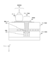
- FIG. 1 is a cross-sectional view showing a first structural example of a semiconductor device according to an embodiment of the present technology.
- the first structural example of the semiconductor device in this embodiment includes a laminated substrate in which a sensor substrate 110 is laminated on a logic substrate 120.
- the logic board 120 includes wiring 130 and an electrode pad 140 connected to the wiring 130. That is, the electrode pad 140 is formed at a depth that penetrates the sensor substrate 110 from the surface of the sensor substrate 110.
- the depth at which the electrode pad 140 is formed is assumed to be, for example, 1 micrometer or more, and more specifically, about 10 micrometer.
- a conductive portion 150 is formed in the region from the electrode pad 140 to the surface of the sensor substrate 110. As will be described later, the conductive portion 150 is formed by repeating a procedure of applying the conductive paste in the region from the electrode pad 140 to the surface of the sensor substrate 110 and a procedure of curing the applied conductive paste.
- the conductive portion 150 includes a wiring region 151 for making a wiring and an electrical connection at a position directly above the electrode pad 140 on the surface of the sensor substrate 110.
- the wiring region 151 has a state in which it can be electrically connected to the wire bonding ball 290. Further, this wiring region 151 has a larger area than the electrode pad 140.
- the ball 290 is a spherical member formed at the tip of the wiring when the wiring is wire-bonded, and is provided with, for example, gold (Au) as a material.
- the balls 290 are electrically connected in the wiring region of the conductive portion 150.
- the electrical connection position of the ball 290 at the time of wire bonding can be raised from the electrode pad 140 to the surface of the sensor substrate 110.
- FIG. 2 is a top view showing a first arrangement example of the conductive portion 150 of the first structural example of the semiconductor device according to the embodiment of the present technology.
- This first arrangement example is an example in which the conductive portions 150 are arranged in series along the chip edge (X direction) of the sensor substrate 110. Each of the electrode pads 140 is dug in the depth direction (Z direction), and the conductive portion 150 is exposed on the surface of the sensor substrate 110. A ball 290 is electrically connected on the conductive portion 150.
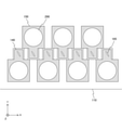
- FIG. 3 is a top view showing a second arrangement example of the conductive portion 150 of the first structural example of the semiconductor device according to the embodiment of the present technology.
- This second arrangement example is an example in which the conductive portion 150 is arranged in a staggered manner along the chip edge (X direction) of the sensor substrate 110. This makes it possible to improve the area efficiency when arranging the conductive portion 150 on the sensor substrate 110 and to reduce the size of the semiconductor device.
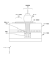
- FIG. 4 is a cross-sectional view showing a second structural example of the semiconductor device according to the embodiment of the present technology.
- the second structural example of the semiconductor device in this embodiment includes a laminated substrate in which the sensor substrate 110 is laminated on the logic substrate 120, as in the first structural example described above.
- the logic board 120 includes wiring 130 and an electrode pad 140 connected to the wiring 130. That is, the electrode pad 140 is formed at a depth that penetrates the sensor substrate 110 from the surface of the sensor substrate 110. Then, the conductive portion 150 is formed in the region from the electrode pad 140 to the surface of the sensor substrate 110.
- the conductive portion 150 includes a probe region 152 for contacting a probe such as a test device at a position directly above the electrode pad 140 on the surface of the sensor substrate 110. Further, the conductive portion 150 includes a wiring region 151 for making an electrical connection with the wiring at a position different from directly above the electrode pad 140 on the surface of the sensor substrate 110. Further, this wiring region 151 has a larger area than the electrode pad 140.
- the electrical connection position of the wire bonding is raised from the electrode pad 140 to the wiring region 151 on the surface of the sensor substrate 110, and the probe region for contacting the probe. 152 can be provided.
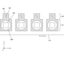
- FIG. 5 is a top view showing a first arrangement example of the conductive portion 150 of the second structural example of the semiconductor device according to the embodiment of the present technology.
- This first arrangement example is an example in which the conductive portions 150 are arranged in series along the chip edge (X direction) of the sensor substrate 110. Each of the electrode pads 140 is dug in the depth direction (Z direction), and the conductive portion 150 is exposed on the surface of the sensor substrate 110.
- the ball 290 is electrically connected to the wiring region 151 of the conductive portion 150. Further, the probe region 152 of the conductive portion 150 is provided with a region for contacting the probe.
- FIG. 6 is a top view showing a second arrangement example of the conductive portion 150 of the second structural example of the semiconductor device according to the embodiment of the present technology.
- This second arrangement example is an example in which the conductive portion 150 is arranged in a staggered manner along the chip edge (X direction) of the sensor substrate 110. This makes it possible to improve the area efficiency when arranging the conductive portion 150 on the sensor substrate 110 and to reduce the size of the semiconductor device.
- FIG. 7 is a cross-sectional view showing a third structural example of the semiconductor device according to the embodiment of the present technology.
- the third structural example of the semiconductor device in this embodiment includes a laminated substrate in which the sensor substrate 110 is laminated on the logic substrate 120, as in the first structural example described above.
- the logic board 120 includes wiring 130 and an electrode pad 140 connected to the wiring 130. That is, the electrode pad 140 is formed at a depth that penetrates the sensor substrate 110 from the surface of the sensor substrate 110. Then, the conductive portion 150 is formed in the region from the electrode pad 140 to the surface of the sensor substrate 110.
- the conductive portion 150 includes a wiring region 151 for making a wiring and an electrical connection at a position directly above the electrode pad 140 on the surface of the sensor substrate 110.
- This wiring region 151 has a larger area than the electrode pad 140.
- the conductive portion 150 includes a probe region 152 on the surface of the sensor substrate 110 at a position different from directly above the electrode pad 140 for contacting a probe such as a test device. That is, as compared with the second structural example described above, the positions of the wiring region 151 and the probe region 152 are interchanged.
- FIG. 8 is a top view showing a first arrangement example of the conductive portion 150 of the third structural example of the semiconductor device according to the embodiment of the present technology.
- This first arrangement example is an example in which the conductive portions 150 are arranged in series along the chip edge (X direction) of the sensor substrate 110. Each of the electrode pads 140 is dug in the depth direction (Z direction), and the conductive portion 150 is exposed on the surface of the sensor substrate 110.
- the ball 290 is electrically connected to the wiring region 151 of the conductive portion 150. Further, the probe region 152 of the conductive portion 150 is provided with a region for contacting the probe.
- FIG. 9 is a top view showing a second arrangement example of the conductive portion 150 of the third structural example of the semiconductor device according to the embodiment of the present technology.
- This second arrangement example is an example in which the conductive portion 150 is arranged in a staggered manner along the chip edge (X direction) of the sensor substrate 110. This makes it possible to improve the area efficiency when arranging the conductive portion 150 on the sensor substrate 110 and to reduce the size of the semiconductor device.
- the first to third structural examples of the semiconductor device in the above-described embodiment can be manufactured by the manufacturing method exemplified below.
- the first manufacturing method example is an example in which the conductive paste is applied by discharging the conductive paste from a position directly above the electrode pad.
- the second manufacturing method example is an example in which the conductive paste is applied from above a mask having an opening at a position directly above the electrode pad.
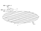
- FIG. 10 is a diagram showing an example of a mode in which the conductive paste 850 is applied to the wafer 810 in the first manufacturing method of the semiconductor device according to the embodiment of the present technology.
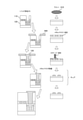
- FIG. 11 is a cross-sectional view showing an example of the application of the conductive paste 850 in the first manufacturing method of the semiconductor device according to the embodiment of the present technology.
- This first manufacturing method example is a method in which the conductive paste coating head 820 is scanned on the surface of the wafer 810, and the conductive paste 850 is discharged and applied only to the position corresponding to the electrode pad 140, and the layers are laminated.
- the conductive paste 850 is a paste-like member having conductivity, and is manufactured, for example, by mixing a resin with a metal powder such as silver (Ag) or copper (Cu).
- the conductive paste 850 may be, for example, a conductive nanopaste.
- a method of ejecting and applying such a conductive paste 850 for example, an inkjet method, a dispense method, an aerosol jet method, or the like is assumed.
- a method of curing the applied conductive paste 850 for example, a method of irradiating light or heat, a laser cure using a laser, or the like is assumed.
- FIG. 12 is a flow chart showing an example of a processing procedure of the first manufacturing method of the semiconductor device according to the embodiment of the present technology.
- the target wafer 810 is prepared (step S911), and the wafer 810 is set in the conductive paste coating device (step S912).
- the conductive paste 850 is applied by discharging (dispensing) the conductive paste 850 on the surface of the electrode pad 140 using the conductive paste coating head 820 of the conductive paste coating device (step S915). Then, the applied conductive paste 850 is cured by light or heat irradiation or laser curing (step S916).
- step S917 No.
- step S917 Yes
- the wafer 810 is taken out from the conductive paste coating device (step S918).
- FIG. 13 is a diagram showing an example of a mode in which the conductive paste 850 is applied to the wafer 810 in the second manufacturing method of the semiconductor device according to the embodiment of the present technology.
- This second manufacturing method example is a method in which a metal mask 880 having an opening at a position corresponding to an electrode pad 140 is attached to the surface of a wafer 810, a conductive paste 850 is applied using a squeegee 890, and the layers are laminated.
- the Squeegee 890 is a spatula-shaped tool. By pressing the squeegee 890 with the conductive paste 850 piled on the metal mask 880, the conductive paste 850 is applied through the opening of the metal mask 880.
- the method of curing the applied conductive paste 850 is the same as that of the first manufacturing method example described above, and for example, a method of irradiating light or heat, a laser cure using a laser, or the like is assumed.
- FIG. 14 is a flow chart showing an example of a processing procedure of the second manufacturing method of the semiconductor device according to the embodiment of the present technology.
- a target wafer 810 is prepared (step S921), a resist is applied to the wafer 810 (step S922), UV exposure is applied (step S923), and the wafer is developed (step S924) to obtain a metal mask 880. To generate.
- the conductive paste 850 is applied through the opening of the metal mask 880 (step S925). Then, the applied conductive paste 850 is cured by light or heat irradiation or laser curing (step S926).
- step S925 The coating procedure (step S925) and the curing procedure (step S926) of these conductive pastes 850 are repeated until the conductive paste 850 is laminated on the surface of the sensor substrate 110 (step S927: No).
- step S927: Yes the resist is peeled off (step S928).
- the electrical connection position of the ball 290 at the time of wire bonding is determined from the electrode pad 140. It can be pulled up to the surface of the sensor board 110.
- the circuit design for forming the semiconductor device is optimized, the wiring for pulling up the electrode, and the construction of the via formation process for that purpose. It is expected that the number of processes will increase and the value will be high.
- the size of the semiconductor device can be reduced by making the electrode itself smaller, applying a conductive paste discharged so as to fill the electrode, or laminating by the squeegee method and pulling out the electrode on the surface of the semiconductor device to form a new one. It is possible to simplify the manufacturing process and the manufacturing process.
- the electrode by being able to pull out the electrode on the surface of the semiconductor device, it is possible to bond the electrode with the optimum wire bond shape using wire bond technology represented by gold wire, and whether it is properly bonded. It is possible to measure on the surface of a semiconductor device.
- the present technology can have the following configurations.
- the predetermined depth is 1 micrometer or more.
- the conductive portion includes a wiring region for making an electrical connection with the wiring at a position directly above the electrode pad on the surface of the substrate.
- the wiring region has a larger area than the electrode pad.
- the conductive portion further includes a probe region for contacting the probe at a position on the surface of the substrate different from directly above the electrode pad.
- the conductive portion includes a wiring region for making an electrical connection with the wiring at a position different from directly above the electrode pad on the surface of the substrate. .. (7) The semiconductor device according to (6) above, wherein the conductive portion further includes a probe region for bringing the probe into contact with a position directly above the electrode pad on the surface of the substrate.
- the semiconductor device according to any one of (1) to (7) above, wherein a plurality of sets of the electrode pads and the conductive portions are arranged in a staggered pattern along the edge of the substrate.
- the substrate is a laminated substrate in which a plurality of substrates are laminated.
- the electrode pad is formed on a substrate other than the outermost substrate among the laminated substrates.
- the semiconductor device according to any one of (1) to (9) above, wherein the conductive portion is embedded in a region up to the surface of the laminated substrate.
- (11) A procedure for forming an electrode pad at a predetermined depth from the surface of the substrate, and The procedure for applying the conductive paste in the region from the electrode pad to the surface of the substrate, and The procedure for curing the applied conductive paste is provided.
- a method for manufacturing a semiconductor device which repeats a procedure of applying the conductive paste and a procedure of curing until the conductive paste is in a state of being electrically connectable to wiring on the surface of the substrate.
- the procedure for applying the conductive paste is as follows. A procedure for generating a mask having an opening directly above the electrode pad, and The method for manufacturing a semiconductor device according to (11) above, which comprises a procedure for applying the conductive paste from above the mask.
Landscapes
- Internal Circuitry In Semiconductor Integrated Circuit Devices (AREA)
- Engineering & Computer Science (AREA)
- Manufacturing & Machinery (AREA)
Abstract
半導体装置の表面から深い位置に電極パッドがある場合において、外部配線との接続を容易にする。 電極パッドは、基板の表面から所定の深さに形成される。導電部は、電極パッドから基板の表面までの領域に形成される。導電部は、基板の表面において、配線と電気的接続可能な状態を有する。導電部は、基板の表面における電極パッドの直上の位置、または、電極パッドの直上とは異なる位置に、配線と電気的接続を行うための配線領域を備える。導電部は、電極パッドから基板の表面までの領域において導電ペーストを塗布する手順と、塗布された導電ペーストを硬化させる手順とを繰り返すことにより形成され得る。
Description
本技術は、半導体装置に関する。詳しくは、基板の表面から深い位置に電極パッドが形成された半導体装置およびその製造方法に関する。
半導体装置においては、外部配線との接続を行う電極パッドを、半導体装置の表面から深い位置に掘り込まれた場所に設けることがある。例えば、電極パッドを露出させて、その電極パッドに対してボンディングワイヤを接続して、実装基板の外部配線と接続する半導体装置が提案されている(例えば、特許文献1参照。)。
上述の従来技術のように電極パッドが深い位置にある場合、金線を使用したワイヤーボンドボールの高さやバンプの高さを高くしなければならなくなる。また、超音波圧着する際に超音波が接合面(例えば、Au-Al界面)に届きにくく、接合不良になりやすい。また、接合したワイヤーボンドの強度測定をするためにシア強度測定をしても、金ボール上部の一部しか削げず、適切な強度測定が難しい。特に、撮像装置に適用した場合、シア強度測定をするために電極の開口を広げると、入射した光が電極に反射することによって画素特性に不具合を生じ、また、撮像装置の大きさが大きくなって装置の小型化が困難になるという問題がある。
本技術はこのような状況に鑑みて生み出されたものであり、半導体装置の表面から深い位置に電極パッドがある場合において、外部配線との接続を容易にすることを目的とする。
本技術は、上述の問題点を解消するためになされたものであり、その第1の側面は、基板の表面から所定の深さに形成された電極パッドと、上記電極パッドから上記基板の表面までの領域に形成されて上記基板の表面において配線と電気的接続可能な状態を有する導電部とを具備する半導体装置である。これにより、電極パッドの上に形成された導電部により、基板の表面において配線と電気的接続させるという作用をもたらす。
また、この第1の側面において、上記所定の深さは、1マイクロメートル以上の深さであってもよい。より具体的には、10マイクロメートル程度の深さであってもよい。
また、この第1の側面において、上記導電部は、上記基板の表面における上記電極パッドの直上の位置に上記配線と電気的接続を行うための配線領域を備えるようにしてもよい。この場合において、上記配線領域は、上記電極パッドよりも広い面積を有するようにしてもよい。また、上記導電部は、上記基板の表面における上記電極パッドの直上とは異なる位置にプローブを接触させるためのプローブ領域をさらに備えてもよい。
また、この第1の側面において、上記導電部は、上記基板の表面における上記電極パッドの直上とは異なる位置に上記配線と電気的接続を行うための配線領域を備えるようにしてもよい。この場合において、上記配線領域は、上記電極パッドよりも広い面積を有するようにしてもよい。また、上記導電部は、上記基板の表面における上記電極パッドの直上の位置にプローブを接触させるためのプローブ領域をさらに備えてもよい。
また、この第1の側面において、複数組の上記電極パッドおよび上記導電部を上記基板のエッジに沿って直列に配置してもよい。また、複数組の上記電極パッドおよび上記導電部を上記基板のエッジに沿って千鳥状に配置してもよい。
また、この第1の側面において、上記基板は複数の基板を積層した積層基板であり、上記電極パッドは、上記積層基板のうち最表面の基板以外の基板に形成され、上記導電部は、上記積層基板の表面までの領域に埋め込まれるようにしてもよい。例えば、積層構造の撮像装置に適用してもよい。
また、本技術の第2の側面は、基板の表面から所定の深さに電極パッドを形成する手順と、上記電極パッドから上記基板の表面までの領域において導電ペーストを塗布する手順と、上記塗布された導電ペーストを硬化させる手順とを具備し、上記導電ペーストが上記基板の表面において配線と電気的接続可能な状態となるまで、上記導電ペーストを塗布する手順および硬化させる手順を繰り返す半導体装置の製造方法である。これにより、導電ペーストの塗布と硬化を繰り返すことにより形成された導電部により、基板の表面において配線と電気的接続させるという作用をもたらす。
また、この第2の側面において、上記導電ペーストを塗布する手順は、上記電極パッドの直上の位置から上記導電ペーストを吐出する手順を備えるようにしてもよい。
また、この第2の側面において、上記導電ペーストを塗布する手順は、上記電極パッドの直上の位置に開口部を備えるマスクを生成する手順と、上記マスクの上から上記導電ペーストを塗布する手順とを備えるようにしてもよい。
以下、本技術を実施するための形態(以下、実施の形態と称する)について説明する。説明は以下の順序により行う。
1.半導体装置の構造
2.半導体装置の製造方法
1.半導体装置の構造
2.半導体装置の製造方法
<1.半導体装置の構造>
[第1の構造例]
図1は、本技術の実施の形態における半導体装置の第1の構造例を示す断面図である。
[第1の構造例]
図1は、本技術の実施の形態における半導体装置の第1の構造例を示す断面図である。
この実施の形態における半導体装置の第1の構造例は、ロジック基板120の上にセンサ基板110を積層した積層基板を備える。ロジック基板120は、配線130を備え、その配線130に接続する電極パッド140を備える。すなわち、センサ基板110の表面から、センサ基板110を貫通した深さに、電極パッド140が形成されている。
ここで、電極パッド140が形成される深さは、例えば1マイクロメートル以上で、より具体的には10マイクロメートル程度が想定される。
電極パッド140からセンサ基板110の表面までの領域には、導電部150が形成される。この導電部150は、後述するように、電極パッド140からセンサ基板110の表面までの領域において導電ペーストを塗布する手順と、塗布された導電ペーストを硬化させる手順とを繰り返すことにより形成される。
この第1の構造例では、導電部150は、センサ基板110の表面における電極パッド140の直上の位置に、配線と電気的接続を行うための配線領域151を備える。この配線領域151は、ワイヤボンディングのボール290と電気的接続可能な状態を有する。また、この配線領域151は、電極パッド140よりも広い面積を有する。
ボール290は、配線をワイヤボンディングする際に配線の先端に形成される球状の部材であり、例えば、金(Au)を材料として備える。ここでは、ボール290は、導電部150の配線領域において電気的に接続される。
この第1の構造例では、導電部150を設けることにより、ワイヤボンディングする際のボール290の電気的接続位置を、電極パッド140からセンサ基板110の表面まで引き上げることができる。
図2は、本技術の実施の形態における半導体装置の第1の構造例の導電部150の第1の配置例を示す上面図である。
この第1の配置例は、導電部150をセンサ基板110のチップエッジ(X方向)に沿って直列に配置した場合の例である。電極パッド140の各々は深さ方向(Z方向)に掘り込まれており、センサ基板110の表面に導電部150が露出している。導電部150の上にはボール290が電気的に接続されている。
図3は、本技術の実施の形態における半導体装置の第1の構造例の導電部150の第2の配置例を示す上面図である。
この第2の配置例は、導電部150をセンサ基板110のチップエッジ(X方向)に沿って千鳥状に配置した場合の例である。これにより、センサ基板110に導電部150を配置する際の面積効率を向上させ、半導体装置を小型化することが可能になる。
[第2の構造例]
図4は、本技術の実施の形態における半導体装置の第2の構造例を示す断面図である。
図4は、本技術の実施の形態における半導体装置の第2の構造例を示す断面図である。
この実施の形態における半導体装置の第2の構造例は、上述の第1の構造例と同様に、ロジック基板120の上にセンサ基板110を積層した積層基板を備える。ロジック基板120は、配線130を備え、その配線130に接続する電極パッド140を備える。すなわち、センサ基板110の表面から、センサ基板110を貫通した深さに、電極パッド140が形成されている。そして、電極パッド140からセンサ基板110の表面までの領域には、導電部150が形成される。
この第2の構造例では、導電部150は、センサ基板110の表面における電極パッド140の直上の位置に、試験装置等のプローブを接触させるためのプローブ領域152を備える。また、導電部150は、センサ基板110の表面における電極パッド140の直上とは異なる位置に、配線と電気的接続を行うための配線領域151を備える。また、この配線領域151は、電極パッド140よりも広い面積を有する。
この第2の構造例では、導電部150を設けることにより、ワイヤボンディングの電気的接続位置を、電極パッド140からセンサ基板110の表面の配線領域151まで引き上げるとともに、プローブを接触させるためのプローブ領域152を設けることができる。
図5は、本技術の実施の形態における半導体装置の第2の構造例の導電部150の第1の配置例を示す上面図である。
この第1の配置例は、導電部150をセンサ基板110のチップエッジ(X方向)に沿って直列に配置した場合の例である。電極パッド140の各々は深さ方向(Z方向)に掘り込まれており、センサ基板110の表面に導電部150が露出している。導電部150の配線領域151にはボール290が電気的に接続されている。また、導電部150のプローブ領域152にはプローブを接触させるための領域が用意されている。
図6は、本技術の実施の形態における半導体装置の第2の構造例の導電部150の第2の配置例を示す上面図である。
この第2の配置例は、導電部150をセンサ基板110のチップエッジ(X方向)に沿って千鳥状に配置した場合の例である。これにより、センサ基板110に導電部150を配置する際の面積効率を向上させ、半導体装置を小型化することが可能になる。
[第3の構造例]
図7は、本技術の実施の形態における半導体装置の第3の構造例を示す断面図である。
図7は、本技術の実施の形態における半導体装置の第3の構造例を示す断面図である。
この実施の形態における半導体装置の第3の構造例は、上述の第1の構造例と同様に、ロジック基板120の上にセンサ基板110を積層した積層基板を備える。ロジック基板120は、配線130を備え、その配線130に接続する電極パッド140を備える。すなわち、センサ基板110の表面から、センサ基板110を貫通した深さに、電極パッド140が形成されている。そして、電極パッド140からセンサ基板110の表面までの領域には、導電部150が形成される。
この第3の構造例では、導電部150は、センサ基板110の表面における電極パッド140の直上の位置に、配線と電気的接続を行うための配線領域151を備える。この配線領域151は、電極パッド140よりも広い面積を有する。また、導電部150は、センサ基板110の表面における電極パッド140の直上とは異なる位置に、試験装置等のプローブを接触させるためのプローブ領域152を備える。すなわち、上述の第2の構造例と比べて、配線領域151とプローブ領域152の位置が入れ替わった構造となっている。
図8は、本技術の実施の形態における半導体装置の第3の構造例の導電部150の第1の配置例を示す上面図である。
この第1の配置例は、導電部150をセンサ基板110のチップエッジ(X方向)に沿って直列に配置した場合の例である。電極パッド140の各々は深さ方向(Z方向)に掘り込まれており、センサ基板110の表面に導電部150が露出している。導電部150の配線領域151にはボール290が電気的に接続されている。また、導電部150のプローブ領域152にはプローブを接触させるための領域が用意されている。
図9は、本技術の実施の形態における半導体装置の第3の構造例の導電部150の第2の配置例を示す上面図である。
この第2の配置例は、導電部150をセンサ基板110のチップエッジ(X方向)に沿って千鳥状に配置した場合の例である。これにより、センサ基板110に導電部150を配置する際の面積効率を向上させ、半導体装置を小型化することが可能になる。
<2.半導体装置の製造方法>
上述の実施の形態における半導体装置の第1乃至第3の構造例は、以下に例示する製造方法により製造することができる。第1の製造方法例は、電極パッドの直上の位置から導電ペーストを吐出することにより導電ペーストを塗布する例である。第2の製造方法例は、電極パッドの直上の位置に開口部を備えるマスクの上から導電ペーストを塗布する例である。
上述の実施の形態における半導体装置の第1乃至第3の構造例は、以下に例示する製造方法により製造することができる。第1の製造方法例は、電極パッドの直上の位置から導電ペーストを吐出することにより導電ペーストを塗布する例である。第2の製造方法例は、電極パッドの直上の位置に開口部を備えるマスクの上から導電ペーストを塗布する例である。
[第1の製造方法例]
図10は、本技術の実施の形態の半導体装置の第1の製造方法におけるウエハ810に対する導電ペースト850の塗布の態様例を示す図である。図11は、本技術の実施の形態の半導体装置の第1の製造方法における導電ペースト850の塗布の態様例を示す断面図である。
図10は、本技術の実施の形態の半導体装置の第1の製造方法におけるウエハ810に対する導電ペースト850の塗布の態様例を示す図である。図11は、本技術の実施の形態の半導体装置の第1の製造方法における導電ペースト850の塗布の態様例を示す断面図である。
この第1の製造方法例は、導電ペースト塗布ヘッド820をウエハ810に表面で走査し、電極パッド140に相当する位置のみに導電ペースト850を吐出して塗布し、積層していく手法である。
導電ペースト850は、導電性を有するペースト状部材であり、例えば樹脂に銀(Ag)や銅(Cu)などの金属粉末を混ぜ合わせることにより製造される。導電ペースト850は、例えば導電ナノペーストであってもよい。
このような導電ペースト850を吐出して塗布する方式としては、例えば、インクジェット方式、ディスペンス方式、エアロゾルジェット方式などが想定される。
塗布された導電ペースト850を硬化させる手法としては、例えば、光または熱を照射する手法や、レーザを使用したレーザキュアなどが想定される。
図12は、本技術の実施の形態の半導体装置の第1の製造方法の処理手順例を示す流れ図である。
まず、対象となるウエハ810を準備して(ステップS911)、そのウエハ810を導電ペースト塗布装置にセッティングする(ステップS912)。
次に、導電ペースト塗布装置の導電ペースト塗布ヘッド820を用いて、電極パッド140の表面に導電ペースト850を吐出(ディスペンス)することにより塗布する(ステップS915)。そして、塗布した導電ペースト850を、光または熱照射や、レーザキュアにより硬化させる(ステップS916)。
これらの導電ペースト850の塗布手順(ステップS915)と、硬化手順(ステップS916)とを、センサ基板110の表面に導電ペースト850が積層されるようになるまで繰り返し行う(ステップS917:No)。
これら一連の処理が終了すると(ステップS917:Yes)、導電ペースト塗布装置からウエハ810を取り出す(ステップS918)。
[第2の製造方法例]
図13は、本技術の実施の形態の半導体装置の第2の製造方法におけるウエハ810に対する導電ペースト850の塗布の態様例を示す図である。
図13は、本技術の実施の形態の半導体装置の第2の製造方法におけるウエハ810に対する導電ペースト850の塗布の態様例を示す図である。
この第2の製造方法例は、電極パッド140に相当する位置を開口したメタルマスク880をウエハ810表面に張り付けて、スキージ890を用いて導電ペースト850を塗布し、積層していく手法である。
スキージ(Squeegee)890は、へら状の道具である。メタルマスク880の上に導電ペースト850を盛った状態でスキージ890を押し付けることにより、メタルマスク880の開口を介して導電ペースト850が塗布される。
塗布された導電ペースト850を硬化させる手法は、上述の第1の製造方法例と同様であり、例えば、光または熱を照射する手法や、レーザを使用したレーザキュアなどが想定される。
図14は、本技術の実施の形態の半導体装置の第2の製造方法の処理手順例を示す流れ図である。
まず、対象となるウエハ810を準備して(ステップS921)、そのウエハ810にレジストを塗布し(ステップS922)、UV露光して(ステップS923)、現像することにより(ステップS924)、メタルマスク880を生成する。
次に、スキージ890を用いて、メタルマスク880の開口を介して導電ペースト850を塗布する(ステップS925)。そして、塗布した導電ペースト850を、光または熱照射や、レーザキュアにより硬化させる(ステップS926)。
これらの導電ペースト850の塗布手順(ステップS925)と、硬化手順(ステップS926)とを、センサ基板110の表面に導電ペースト850が積層されるようになるまで繰り返し行う(ステップS927:No)。
これら一連の処理が終了すると(ステップS927:Yes)、レジストを剥離する(ステップS928)。
このように、本技術の実施の形態によれば、導電ペースト850の塗布と硬化を繰り返して導電部150を形成することにより、ワイヤボンディングの際のボール290の電気的接続位置を電極パッド140からセンサ基板110の表面まで引き上げることができる。
半導体装置の表面から深い位置にある電極を、半導体製造プロセスで表面に引き上げようとすると、半導体装置を形成する回路デザインの最適化、電極を引き上げるための配線、ビアの形成プロセスの構築、そのためのプロセス増加が発生し、高付加価値となることが予想される。これに対し、この実施の形態では、半導体製造プロセスを使用することなく、既存の組立工程の組合せで、安価に深い位置の電極を引き上げることが可能となる。また、電極自体を小さくし、電極を埋めるように吐出した導電性ペーストを塗布し、または、スキージ工法により積層し、半導体装置の表面に電極を引き出して新たに形成することにより、半導体装置の小型化や製造プロセスの簡略化を図ることができる。さらに、半導体装置の表面に電極を引き出せることで、金線に代表されるワイヤーボンド技術を使用して、最適なワイヤーボンド形状で電極との接合が可能となり、また、適切に接合されているかを半導体装置表面で測定することが可能となる。
なお、上述の実施の形態は本技術を具現化するための一例を示したものであり、実施の形態における事項と、特許請求の範囲における発明特定事項とはそれぞれ対応関係を有する。同様に、特許請求の範囲における発明特定事項と、これと同一名称を付した本技術の実施の形態における事項とはそれぞれ対応関係を有する。ただし、本技術は実施の形態に限定されるものではなく、その要旨を逸脱しない範囲において実施の形態に種々の変形を施すことにより具現化することができる。
なお、本明細書に記載された効果はあくまで例示であって、限定されるものではなく、また、他の効果があってもよい。
なお、本技術は以下のような構成もとることができる。
(1)基板の表面から所定の深さに形成された電極パッドと、
前記電極パッドから前記基板の表面までの領域に形成されて前記基板の表面において配線と電気的接続可能な状態を有する導電部と
を具備する半導体装置。
(2)前記所定の深さは、1マイクロメートル以上の深さである
前記(1)に記載の半導体装置。
(3)前記導電部は、前記基板の表面における前記電極パッドの直上の位置に前記配線と電気的接続を行うための配線領域を備える
前記(1)または(2)に記載の半導体装置。
(4)前記配線領域は、前記電極パッドよりも広い面積を有する
前記(3)に記載の半導体装置。
(5)前記導電部は、前記基板の表面における前記電極パッドの直上とは異なる位置にプローブを接触させるためのプローブ領域をさらに備える
前記(3)または(4)に記載の半導体装置。
(6)前記導電部は、前記基板の表面における前記電極パッドの直上とは異なる位置に前記配線と電気的接続を行うための配線領域を備える
前記(1)または(2)に記載の半導体装置。
(7)前記導電部は、前記基板の表面における前記電極パッドの直上の位置にプローブを接触させるためのプローブ領域をさらに備える
前記(6)に記載の半導体装置。
(8)複数組の前記電極パッドおよび前記導電部を前記基板のエッジに沿って直列に配置した前記(1)から(7)のいずれかに記載の半導体装置。
(9)複数組の前記電極パッドおよび前記導電部を前記基板のエッジに沿って千鳥状に配置した前記(1)から(7)のいずれかに記載の半導体装置。
(10)前記基板は複数の基板を積層した積層基板であり、
前記電極パッドは、前記積層基板のうち最表面の基板以外の基板に形成され、
前記導電部は、前記積層基板の表面までの領域に埋め込まれる
前記(1)から(9)のいずれかに記載の半導体装置。
(11)基板の表面から所定の深さに電極パッドを形成する手順と、
前記電極パッドから前記基板の表面までの領域において導電ペーストを塗布する手順と、
前記塗布された導電ペーストを硬化させる手順とを具備し、
前記導電ペーストが前記基板の表面において配線と電気的接続可能な状態となるまで、前記導電ペーストを塗布する手順および硬化させる手順を繰り返す
半導体装置の製造方法。
(12)前記導電ペーストを塗布する手順は、前記電極パッドの直上の位置から前記導電ペーストを吐出する手順を備える
前記(11)に記載の半導体装置の製造方法。
(13)前記導電ペーストを塗布する手順は、
前記電極パッドの直上の位置に開口部を備えるマスクを生成する手順と、
前記マスクの上から前記導電ペーストを塗布する手順と
を備える
前記(11)に記載の半導体装置の製造方法。
(1)基板の表面から所定の深さに形成された電極パッドと、
前記電極パッドから前記基板の表面までの領域に形成されて前記基板の表面において配線と電気的接続可能な状態を有する導電部と
を具備する半導体装置。
(2)前記所定の深さは、1マイクロメートル以上の深さである
前記(1)に記載の半導体装置。
(3)前記導電部は、前記基板の表面における前記電極パッドの直上の位置に前記配線と電気的接続を行うための配線領域を備える
前記(1)または(2)に記載の半導体装置。
(4)前記配線領域は、前記電極パッドよりも広い面積を有する
前記(3)に記載の半導体装置。
(5)前記導電部は、前記基板の表面における前記電極パッドの直上とは異なる位置にプローブを接触させるためのプローブ領域をさらに備える
前記(3)または(4)に記載の半導体装置。
(6)前記導電部は、前記基板の表面における前記電極パッドの直上とは異なる位置に前記配線と電気的接続を行うための配線領域を備える
前記(1)または(2)に記載の半導体装置。
(7)前記導電部は、前記基板の表面における前記電極パッドの直上の位置にプローブを接触させるためのプローブ領域をさらに備える
前記(6)に記載の半導体装置。
(8)複数組の前記電極パッドおよび前記導電部を前記基板のエッジに沿って直列に配置した前記(1)から(7)のいずれかに記載の半導体装置。
(9)複数組の前記電極パッドおよび前記導電部を前記基板のエッジに沿って千鳥状に配置した前記(1)から(7)のいずれかに記載の半導体装置。
(10)前記基板は複数の基板を積層した積層基板であり、
前記電極パッドは、前記積層基板のうち最表面の基板以外の基板に形成され、
前記導電部は、前記積層基板の表面までの領域に埋め込まれる
前記(1)から(9)のいずれかに記載の半導体装置。
(11)基板の表面から所定の深さに電極パッドを形成する手順と、
前記電極パッドから前記基板の表面までの領域において導電ペーストを塗布する手順と、
前記塗布された導電ペーストを硬化させる手順とを具備し、
前記導電ペーストが前記基板の表面において配線と電気的接続可能な状態となるまで、前記導電ペーストを塗布する手順および硬化させる手順を繰り返す
半導体装置の製造方法。
(12)前記導電ペーストを塗布する手順は、前記電極パッドの直上の位置から前記導電ペーストを吐出する手順を備える
前記(11)に記載の半導体装置の製造方法。
(13)前記導電ペーストを塗布する手順は、
前記電極パッドの直上の位置に開口部を備えるマスクを生成する手順と、
前記マスクの上から前記導電ペーストを塗布する手順と
を備える
前記(11)に記載の半導体装置の製造方法。
110 センサ基板
120 ロジック基板
130 配線
140 電極パッド
150 導電部
151 配線領域
152 プローブ領域
290 ボール
810 ウエハ
820 導電ペースト塗布ヘッド
850 導電ペースト
880 メタルマスク
890 スキージ
120 ロジック基板
130 配線
140 電極パッド
150 導電部
151 配線領域
152 プローブ領域
290 ボール
810 ウエハ
820 導電ペースト塗布ヘッド
850 導電ペースト
880 メタルマスク
890 スキージ
Claims (13)
- 基板の表面から所定の深さに形成された電極パッドと、
前記電極パッドから前記基板の表面までの領域に形成されて前記基板の表面において配線と電気的接続可能な状態を有する導電部と
を具備する半導体装置。 - 前記所定の深さは、1マイクロメートル以上の深さである
請求項1記載の半導体装置。 - 前記導電部は、前記基板の表面における前記電極パッドの直上の位置に前記配線と電気的接続を行うための配線領域を備える
請求項1記載の半導体装置。 - 前記配線領域は、前記電極パッドよりも広い面積を有する
請求項3記載の半導体装置。 - 前記導電部は、前記基板の表面における前記電極パッドの直上とは異なる位置にプローブを接触させるためのプローブ領域をさらに備える
請求項3記載の半導体装置。 - 前記導電部は、前記基板の表面における前記電極パッドの直上とは異なる位置に前記配線と電気的接続を行うための配線領域を備える
請求項1記載の半導体装置。 - 前記導電部は、前記基板の表面における前記電極パッドの直上の位置にプローブを接触させるためのプローブ領域をさらに備える
請求項6記載の半導体装置。 - 複数組の前記電極パッドおよび前記導電部を前記基板のエッジに沿って直列に配置した請求項1記載の半導体装置。
- 複数組の前記電極パッドおよび前記導電部を前記基板のエッジに沿って千鳥状に配置した請求項1記載の半導体装置。
- 前記基板は複数の基板を積層した積層基板であり、
前記電極パッドは、前記積層基板のうち最表面の基板以外の基板に形成され、
前記導電部は、前記積層基板の表面までの領域に埋め込まれる
請求項1記載の半導体装置。 - 基板の表面から所定の深さに電極パッドを形成する手順と、
前記電極パッドから前記基板の表面までの領域において導電ペーストを塗布する手順と、
前記塗布された導電ペーストを硬化させる手順とを具備し、
前記導電ペーストが前記基板の表面において配線と電気的接続可能な状態となるまで、前記導電ペーストを塗布する手順および硬化させる手順を繰り返す
半導体装置の製造方法。 - 前記導電ペーストを塗布する手順は、前記電極パッドの直上の位置から前記導電ペーストを吐出する手順を備える
請求項11記載の半導体装置の製造方法。 - 前記導電ペーストを塗布する手順は、
前記電極パッドの直上の位置に開口部を備えるマスクを生成する手順と、
前記マスクの上から前記導電ペーストを塗布する手順と
を備える
請求項11記載の半導体装置の製造方法。
Priority Applications (2)
| Application Number | Priority Date | Filing Date | Title |
|---|---|---|---|
| JP2022538610A JP7660125B2 (ja) | 2020-07-20 | 2021-05-26 | 半導体装置およびその製造方法 |
| US18/005,010 US20230253269A1 (en) | 2020-07-20 | 2021-05-26 | Semiconductor device and method for manufacturing the same |
Applications Claiming Priority (2)
| Application Number | Priority Date | Filing Date | Title |
|---|---|---|---|
| JP2020-123408 | 2020-07-20 | ||
| JP2020123408 | 2020-07-20 |
Publications (1)
| Publication Number | Publication Date |
|---|---|
| WO2022018961A1 true WO2022018961A1 (ja) | 2022-01-27 |
Family
ID=79728620
Family Applications (1)
| Application Number | Title | Priority Date | Filing Date |
|---|---|---|---|
| PCT/JP2021/020006 Ceased WO2022018961A1 (ja) | 2020-07-20 | 2021-05-26 | 半導体装置およびその製造方法 |
Country Status (3)
| Country | Link |
|---|---|
| US (1) | US20230253269A1 (ja) |
| JP (1) | JP7660125B2 (ja) |
| WO (1) | WO2022018961A1 (ja) |
Citations (3)
| Publication number | Priority date | Publication date | Assignee | Title |
|---|---|---|---|---|
| JP2001015516A (ja) * | 1999-06-30 | 2001-01-19 | Toshiba Corp | 半導体装置及びその製造方法 |
| JP2005527968A (ja) * | 2002-03-13 | 2005-09-15 | フリースケール セミコンダクター インコーポレイテッド | ボンドパッドを有する半導体装置およびそのための方法 |
| JP2010114390A (ja) * | 2008-11-10 | 2010-05-20 | Panasonic Corp | 半導体装置および半導体装置の製造方法 |
Family Cites Families (2)
| Publication number | Priority date | Publication date | Assignee | Title |
|---|---|---|---|---|
| JP5729100B2 (ja) * | 2011-04-11 | 2015-06-03 | ソニー株式会社 | 半導体装置の製造方法、半導体装置、電子機器 |
| JP6538960B2 (ja) * | 2016-02-23 | 2019-07-03 | ルネサスエレクトロニクス株式会社 | 半導体装置およびその製造方法 |
-
2021
- 2021-05-26 WO PCT/JP2021/020006 patent/WO2022018961A1/ja not_active Ceased
- 2021-05-26 JP JP2022538610A patent/JP7660125B2/ja active Active
- 2021-05-26 US US18/005,010 patent/US20230253269A1/en active Pending
Patent Citations (3)
| Publication number | Priority date | Publication date | Assignee | Title |
|---|---|---|---|---|
| JP2001015516A (ja) * | 1999-06-30 | 2001-01-19 | Toshiba Corp | 半導体装置及びその製造方法 |
| JP2005527968A (ja) * | 2002-03-13 | 2005-09-15 | フリースケール セミコンダクター インコーポレイテッド | ボンドパッドを有する半導体装置およびそのための方法 |
| JP2010114390A (ja) * | 2008-11-10 | 2010-05-20 | Panasonic Corp | 半導体装置および半導体装置の製造方法 |
Also Published As
| Publication number | Publication date |
|---|---|
| JPWO2022018961A1 (ja) | 2022-01-27 |
| JP7660125B2 (ja) | 2025-04-10 |
| US20230253269A1 (en) | 2023-08-10 |
Similar Documents
| Publication | Publication Date | Title |
|---|---|---|
| TWI588949B (zh) | 具有整合式承載表面的微電子封裝 | |
| US8659151B2 (en) | Semiconductor device and manufacturing method thereof | |
| US7745322B2 (en) | Wire bond interconnection | |
| EP2852974B1 (en) | Method of making a substrate-less stackable package with wire-bond interconnect | |
| US8816514B2 (en) | Microelectronic assembly with joined bond elements having lowered inductance | |
| CN105074914B (zh) | 具有接线键合过孔的微电子封装体及其制作方法以及用于微电子封装体的加强层 | |
| CN108269792A (zh) | 瀑布引线键合 | |
| TW201505145A (zh) | 半導體裝置及其製造方法 | |
| CN101281876A (zh) | 半导体器件的制造方法以及半导体器件 | |
| US6400034B1 (en) | Semiconductor device | |
| JP2006134912A (ja) | 半導体モジュールおよびその製造方法、ならびにフィルムインターポーザ | |
| KR20060101385A (ko) | 반도체 장치 및 그 제조 방법 | |
| TW471077B (en) | Bump forming method, bump forming bonding tool, semiconductor wafer, semiconductor chip, semiconductor device, manufacture thereof, circuit board and electronic machine | |
| CN108346640B (zh) | 半导体结构及其制作方法 | |
| JP7660125B2 (ja) | 半導体装置およびその製造方法 | |
| US20100269333A1 (en) | Method for Mounting Flip Chip and Substrate Used Therein | |
| JP2010161222A (ja) | 半導体パッケージの製造方法、半導体パッケージ及び半導体チップ | |
| CN1315168C (zh) | 晶圆级封装制作工艺及其晶片结构 | |
| KR100968008B1 (ko) | 반도체장치 및 그 제조방법 | |
| JP2003234427A (ja) | 配線基板、それを用いた半導体装置、それらの製造方法 | |
| CN119601477A (zh) | 热超声球形金丝键合的金凸点制备方法、倒装键合结构及芯片 | |
| JP4698387B2 (ja) | 半導体装置及びその製造方法 | |
| CN1442891A (zh) | 软式封装构造及其制作方法 | |
| JPH06338539A (ja) | 半導体素子の接続方法 | |
| CN115642139A (zh) | 半导体结构及其制作方法 |
Legal Events
| Date | Code | Title | Description |
|---|---|---|---|
| 121 | Ep: the epo has been informed by wipo that ep was designated in this application |
Ref document number: 21845456 Country of ref document: EP Kind code of ref document: A1 |
|
| ENP | Entry into the national phase |
Ref document number: 2022538610 Country of ref document: JP Kind code of ref document: A |
|
| NENP | Non-entry into the national phase |
Ref country code: DE |
|
| 122 | Ep: pct application non-entry in european phase |
Ref document number: 21845456 Country of ref document: EP Kind code of ref document: A1 |