WO2022018859A1 - ダイヤモンドの加工方法、ダイヤモンド基板の製造方法、および半導体装置の製造方法 - Google Patents
ダイヤモンドの加工方法、ダイヤモンド基板の製造方法、および半導体装置の製造方法 Download PDFInfo
- Publication number
- WO2022018859A1 WO2022018859A1 PCT/JP2020/028448 JP2020028448W WO2022018859A1 WO 2022018859 A1 WO2022018859 A1 WO 2022018859A1 JP 2020028448 W JP2020028448 W JP 2020028448W WO 2022018859 A1 WO2022018859 A1 WO 2022018859A1
- Authority
- WO
- WIPO (PCT)
- Prior art keywords
- diamond
- plasma
- processing method
- substrate
- gas
- Prior art date
- Legal status (The legal status is an assumption and is not a legal conclusion. Google has not performed a legal analysis and makes no representation as to the accuracy of the status listed.)
- Ceased
Links
Images





Classifications
-
- C—CHEMISTRY; METALLURGY
- C01—INORGANIC CHEMISTRY
- C01B—NON-METALLIC ELEMENTS; COMPOUNDS THEREOF; METALLOIDS OR COMPOUNDS THEREOF NOT COVERED BY SUBCLASS C01C
- C01B32/00—Carbon; Compounds thereof
- C01B32/25—Diamond
- C01B32/28—After-treatment, e.g. purification, irradiation, separation or recovery
-
- C—CHEMISTRY; METALLURGY
- C30—CRYSTAL GROWTH
- C30B—SINGLE-CRYSTAL GROWTH; UNIDIRECTIONAL SOLIDIFICATION OF EUTECTIC MATERIAL OR UNIDIRECTIONAL DEMIXING OF EUTECTOID MATERIAL; REFINING BY ZONE-MELTING OF MATERIAL; PRODUCTION OF A HOMOGENEOUS POLYCRYSTALLINE MATERIAL WITH DEFINED STRUCTURE; SINGLE CRYSTALS OR HOMOGENEOUS POLYCRYSTALLINE MATERIAL WITH DEFINED STRUCTURE; AFTER-TREATMENT OF SINGLE CRYSTALS OR A HOMOGENEOUS POLYCRYSTALLINE MATERIAL WITH DEFINED STRUCTURE; APPARATUS THEREFOR
- C30B29/00—Single crystals or homogeneous polycrystalline material with defined structure characterised by the material or by their shape
- C30B29/02—Elements
- C30B29/04—Diamond
-
- C—CHEMISTRY; METALLURGY
- C30—CRYSTAL GROWTH
- C30B—SINGLE-CRYSTAL GROWTH; UNIDIRECTIONAL SOLIDIFICATION OF EUTECTIC MATERIAL OR UNIDIRECTIONAL DEMIXING OF EUTECTOID MATERIAL; REFINING BY ZONE-MELTING OF MATERIAL; PRODUCTION OF A HOMOGENEOUS POLYCRYSTALLINE MATERIAL WITH DEFINED STRUCTURE; SINGLE CRYSTALS OR HOMOGENEOUS POLYCRYSTALLINE MATERIAL WITH DEFINED STRUCTURE; AFTER-TREATMENT OF SINGLE CRYSTALS OR A HOMOGENEOUS POLYCRYSTALLINE MATERIAL WITH DEFINED STRUCTURE; APPARATUS THEREFOR
- C30B33/00—After-treatment of single crystals or homogeneous polycrystalline material with defined structure
- C30B33/02—Heat treatment
-
- C—CHEMISTRY; METALLURGY
- C30—CRYSTAL GROWTH
- C30B—SINGLE-CRYSTAL GROWTH; UNIDIRECTIONAL SOLIDIFICATION OF EUTECTIC MATERIAL OR UNIDIRECTIONAL DEMIXING OF EUTECTOID MATERIAL; REFINING BY ZONE-MELTING OF MATERIAL; PRODUCTION OF A HOMOGENEOUS POLYCRYSTALLINE MATERIAL WITH DEFINED STRUCTURE; SINGLE CRYSTALS OR HOMOGENEOUS POLYCRYSTALLINE MATERIAL WITH DEFINED STRUCTURE; AFTER-TREATMENT OF SINGLE CRYSTALS OR A HOMOGENEOUS POLYCRYSTALLINE MATERIAL WITH DEFINED STRUCTURE; APPARATUS THEREFOR
- C30B33/00—After-treatment of single crystals or homogeneous polycrystalline material with defined structure
- C30B33/04—After-treatment of single crystals or homogeneous polycrystalline material with defined structure using electric or magnetic fields or particle radiation
-
- C—CHEMISTRY; METALLURGY
- C30—CRYSTAL GROWTH
- C30B—SINGLE-CRYSTAL GROWTH; UNIDIRECTIONAL SOLIDIFICATION OF EUTECTIC MATERIAL OR UNIDIRECTIONAL DEMIXING OF EUTECTOID MATERIAL; REFINING BY ZONE-MELTING OF MATERIAL; PRODUCTION OF A HOMOGENEOUS POLYCRYSTALLINE MATERIAL WITH DEFINED STRUCTURE; SINGLE CRYSTALS OR HOMOGENEOUS POLYCRYSTALLINE MATERIAL WITH DEFINED STRUCTURE; AFTER-TREATMENT OF SINGLE CRYSTALS OR A HOMOGENEOUS POLYCRYSTALLINE MATERIAL WITH DEFINED STRUCTURE; APPARATUS THEREFOR
- C30B33/00—After-treatment of single crystals or homogeneous polycrystalline material with defined structure
- C30B33/08—Etching
-
- C—CHEMISTRY; METALLURGY
- C30—CRYSTAL GROWTH
- C30B—SINGLE-CRYSTAL GROWTH; UNIDIRECTIONAL SOLIDIFICATION OF EUTECTIC MATERIAL OR UNIDIRECTIONAL DEMIXING OF EUTECTOID MATERIAL; REFINING BY ZONE-MELTING OF MATERIAL; PRODUCTION OF A HOMOGENEOUS POLYCRYSTALLINE MATERIAL WITH DEFINED STRUCTURE; SINGLE CRYSTALS OR HOMOGENEOUS POLYCRYSTALLINE MATERIAL WITH DEFINED STRUCTURE; AFTER-TREATMENT OF SINGLE CRYSTALS OR A HOMOGENEOUS POLYCRYSTALLINE MATERIAL WITH DEFINED STRUCTURE; APPARATUS THEREFOR
- C30B33/00—After-treatment of single crystals or homogeneous polycrystalline material with defined structure
- C30B33/08—Etching
- C30B33/12—Etching in gas atmosphere or plasma
-
- H—ELECTRICITY
- H10—SEMICONDUCTOR DEVICES; ELECTRIC SOLID-STATE DEVICES NOT OTHERWISE PROVIDED FOR
- H10P—GENERIC PROCESSES OR APPARATUS FOR THE MANUFACTURE OR TREATMENT OF DEVICES COVERED BY CLASS H10
- H10P50/00—Etching of wafers, substrates or parts of devices
- H10P50/20—Dry etching; Plasma etching; Reactive-ion etching
- H10P50/24—Dry etching; Plasma etching; Reactive-ion etching of semiconductor materials
- H10P50/242—Dry etching; Plasma etching; Reactive-ion etching of semiconductor materials of Group IV materials
Definitions
- This disclosure relates to a diamond processing method, a diamond substrate manufacturing method, and a semiconductor device manufacturing method.
- Diamond has excellent properties such as the highest thermal conductivity among materials, and various applications such as using a diamond substrate for heat dissipation of a semiconductor device are considered. Although diamond needs to be processed as needed for such applications, it is not easy to process because diamond has the highest hardness of any material.
- CMP chemical mechanical polishing
- the processing speed of the processing method of Patent Document 1 is not sufficient, and it is desirable that diamond can be processed at a higher processing speed.
- This disclosure is made in order to solve the above-mentioned problems, and describes a diamond processing method capable of processing diamond at a high processing speed in a method of processing diamond using plasma, and a diamond processing method. It is an object of the present invention to provide a method for manufacturing a diamond substrate used and a method for manufacturing a semiconductor device using the method for manufacturing the diamond substrate.
- One aspect of the present disclosure is a diamond processing method for processing the surface of diamond using plasma, wherein the surface of diamond is heated using plasma to graphitize the surface of diamond, and then graphite is used. It is a diamond processing method that sublimates.
- another aspect of the diamond processing method of the present disclosure is a diamond processing method of processing the surface of diamond using plasma, in which the surface of diamond is heated by using plasma and the temperature of the surface of diamond is heated. Is a diamond processing method with a temperature of 3700 K or higher.
- another aspect of the diamond processing method of the present disclosure is a diamond processing method for processing the surface of diamond using plasma, the gas temperature of plasma is 3700 K or higher, and diamond is processed using plasma.
- a diamond processing method that heats the surface of a diamond is a diamond processing method for processing the surface of diamond using plasma, the gas temperature of plasma is 3700 K or higher, and diamond is processed using plasma.
- the method for manufacturing a diamond substrate of the present disclosure is a method for manufacturing a diamond substrate, in which a diamond substrate having a surface exposed to diamond is prepared and the surface exposed to diamond is processed by the diamond processing method of the present disclosure. ..
- a diamond substrate manufactured by the method for manufacturing a diamond substrate of the present disclosure is prepared, a material having a surface with an exposed semiconductor layer is prepared, and the surface with an exposed semiconductor layer is used.
- a method for manufacturing a semiconductor device, which directly joins a surface on which diamond processed by a diamond processing method is exposed is exposed.
- One aspect of the present disclosure is a diamond processing method for processing the surface of diamond using plasma, wherein the surface of diamond is heated using plasma to graphitize the surface of diamond, and then graphite is used. It is a diamond processing method that sublimates. This provides a diamond processing method capable of processing diamond at a high processing speed in the method of processing diamond using plasma.
- another aspect of the diamond processing method of the present disclosure is a diamond processing method of processing the surface of diamond using plasma, in which the surface of diamond is heated by using plasma and the temperature of the surface of diamond is heated.
- a diamond processing method with a temperature of 3700 K or higher This provides a diamond processing method capable of processing diamond at a high processing speed in the method of processing diamond using plasma.
- another aspect of the diamond processing method of the present disclosure is a diamond processing method for processing the surface of diamond using plasma, the gas temperature of plasma is 3700 K or higher, and diamond is processed using plasma.
- a diamond processing method that heats the surface of a diamond This provides a diamond processing method capable of processing diamond at a high processing speed in the method of processing diamond using plasma.
- the method for manufacturing a diamond substrate of the present disclosure is a method for manufacturing a diamond substrate, in which a diamond substrate having a surface exposed to diamond is prepared and the surface exposed to diamond is processed by the diamond processing method of the present disclosure. .. This provides a method for manufacturing a diamond substrate using a diamond processing method capable of processing diamond at a high processing speed in a method for processing diamond using plasma.
- a diamond substrate manufactured by the method for manufacturing a diamond substrate of the present disclosure is prepared, a material having a surface with an exposed semiconductor layer is prepared, and the surface with an exposed semiconductor layer is used.
- a method for manufacturing a semiconductor device, which directly joins a surface on which diamond processed by a diamond processing method is exposed is exposed. This provides a method for manufacturing a semiconductor device using a method for manufacturing a diamond substrate using a diamond processing method capable of processing diamond at a high processing speed in a method for processing diamond using plasma.
- FIG. It is a schematic block diagram of the dry etching apparatus of Embodiment 1.
- FIG. It is a schematic diagram explaining the gas introduction through the small hole of the plasma electrode tip portion. It is a schematic diagram which shows the movable mechanism in the XYZ direction and the rotation direction of a substrate stage. It is a schematic diagram which shows the transport
- FIG. 1 is a schematic configuration diagram of a dry etching apparatus 100 which is an example of a dry etching apparatus used for carrying out the diamond processing method of the present embodiment.
- the dry etching apparatus 100 includes a plasma generator 101, a processing container 10, a stage 14, a gas supply unit 102, and an exhaust unit 103.
- FIG. 1 also shows a diamond substrate 4 which is an example of an object to be etched.
- the diamond substrate 4 has a surface 4a on which diamond is exposed, and the surface 4a is etched and processed by the dry etching apparatus 100 (see FIG. 2).
- the plasma generator 101 includes a high-frequency power supply 1, a waveguide 2 having a function of propagating the electric power input from the high-frequency power supply 1, and a plasma electrode 3. It is desirable that the high frequency power supply 1, the waveguide 2, and the plasma electrode 3 are directly connected in order to suppress the propagation loss of the input power as low as possible. However, for example, the high frequency power supply 1 and the waveguide 2 may be connected via a coaxial cable having a relatively low power loss.
- the high frequency power supply 1 use one that can oscillate at a frequency in the microwave band for generating plasma.
- microwave oscillation methods magnetron oscillation type and semiconductor oscillation type
- the magnetron oscillation type is generally used for high-frequency power supplies with a maximum input power of about 1 kW or more.
- the semiconductor oscillation type power supply is used when a magnetron oscillation type power supply is used in a low power region such as 100 W or less where it is difficult to stably supply electric power, or when an oscillation frequency having a narrow bandwidth is used.
- the high frequency power supply 1 may use either oscillation method.
- the waveguide 2 has a low loss of the microwave power input from the high-frequency power supply 1 to the plasma generated between the plasma electrode 3 and the diamond substrate 4 via the plasma electrode 3 inserted into the waveguide 2. It has a function to propagate with.
- the waveguide 2 includes a power measuring instrument 5, a three-stub tuner 6, a movable short-circuit device 7, a directional coupler 8, and a dummy load 9.
- the power measuring instrument 5 monitors the input power from the high frequency power supply 1 and the reflected power from the movable short circuit device 7.
- the three-stub tuner 6 controls the phase of the microwave.
- the waveguide 2 may include an E / H tuner instead of the three-stub tuner 6.
- the movable short circuit 7 is for reflecting microwaves to form a standing wave.
- the directional coupler 8 changes the propagation direction of the microwave propagating in the direction of the high frequency power supply 1 in order to prevent the microwave power reflected by the movable short circuit 7 from entering the high frequency power supply 1.
- the dummy load 9 absorbs the microwave whose propagation direction is changed by the directional coupler 8 and converts the energy into heat.
- One end of the plasma electrode 3 is inserted into the processing container 10 through the waveguide 2.
- the plasma electrode 3 is electrically connected to the high frequency power supply 1 by passing through the waveguide 2.
- the plasma electrode 3 has a pipe-shaped structure.
- the gas introduction port 16 is one is shown in FIG. 2, a plurality of gas introduction ports 16 may be formed on the end surface of the tip end portion of the plasma electrode 3.
- the gas supply unit 102 includes a gas cylinder 40 and a flow rate controller (MFC: Mass Flow Controller) 11, and supplies the gas stored in the gas cylinder 40 to the plasma electrode 3 by controlling the flow rate by the flow rate controller 11. do.
- the gas supplied from the gas supply unit 102 to the plasma electrode 3 passes through the inside of the plasma electrode 3 pipe-shaped structure and is introduced into the processing container 10 through the gas introduction port 16.
- the gas used for the etching process of the diamond substrate 4 in the dry etching apparatus 100 is, for example, an etching gas which is a gas that chemically reacts with diamond, that is, for example, hydrogen gas or oxygen gas.
- a gas containing a rare gas in addition to hydrogen gas or oxygen gas may be used.
- the exhaust unit 103 includes an exhaust valve 12 and a vacuum pump 13.
- the processing container 10 is connected to the vacuum pump 13 via an exhaust valve 12, and the residual gas in the processing container 10 can be exhausted to a low pressure.
- the pressure in the processing container 10 is measured by a pressure gauge (not shown). By adjusting the exhaust amount of the vacuum pump 13 with the exhaust valve 12, the pressure inside the processing container 10 can be controlled to the desired pressure.
- the stage 14 includes a sample holder 15.
- the stage 14 is installed in the processing container 10 and has a function of fixing the diamond substrate 4 by a vacuum chuck via the sample holder 15. Further, the stage 14 is provided with a heating mechanism, and the diamond substrate 4 fixed on the sample holder 15 can be heated to a target temperature.
- the stage 14 is provided with a movable mechanism.
- the stage 14 is moved in the XYZ direction, or in the XZ direction and the rotation direction by the movable mechanism.
- the movable mechanism is controlled by an external device.
- the Z-direction movement of the stage 14 is used to adjust the distance (gap) W (see FIG. 2) between the plasma electrode 3 and the diamond substrate 4.
- Plasma is generated locally corresponding to the area of the end face of the plasma electrode 3, but the plasma is scanned two-dimensionally on the surface 4a of the diamond substrate 4 by the movement in the XY direction or the movement in the X direction and the rotation direction.
- a large area diamond substrate 4 can be etched and processed.
- the stage 14, the processing container 10, and the diamond substrate 4 fixed on the sample holder 15 are connected to the ground potential.
- Diamond processing method The diamond processing method according to the present embodiment and the operation of the dry etching apparatus 100 used at that time will be described.
- the diamond substrate 4 to be flattened by the diamond processing method according to the present embodiment may be either a single crystal diamond substrate or a polycrystalline diamond substrate.
- the polycrystalline diamond substrate is produced by forming a polycrystalline diamond film by a CVD method on a base material wafer of a different material, for example, silicon (Si), silicon carbide (SiC), sapphire (Al 2 O 3), or the like. Therefore, it is more suitable as a substrate for the nitride semiconductor device described in, for example, the third embodiment from the viewpoint of being cheaper and easier to increase the area than a single crystal.
- the diamond substrate 4 is fixed on the sample holder 15 in the processing container 10 with a vacuum chuck, and the inside of the processing container 10 is exhausted to a low pressure by the vacuum pump 13.
- stage 14 is moved in the Z direction to adjust the gap W between the plasma electrode 3 and the diamond substrate 4.
- the gas used for the etching process is introduced into the processing container 10 from the gas introduction port 16 on the end face of the plasma electrode 3.
- the exhaust valve 12 is adjusted to set the processing pressure in the processing container 10 from quasi-atmospheric pressure to about atmospheric pressure, for example, 65 hPa or more and 2000 hPa or less.
- the diamond substrate 4 is heated by the heating mechanism of the stage 14, and finally, microwave power is applied from the high frequency power supply 1, and the three-stub tuner 6 (or E / H tuner) and the movable short-circuiter 7 are used. Impedance matching of microwaves is taken in the propagation path of the waveguide 2, plasma PL is generated, and etching processing is performed. Then, as shown in FIG. 3, the stage 14 is moved in the XY direction, or in the X direction and the rotational direction for scanning while plasma is being generated, and the plasma irradiation region, which is the region where the plasma PL is irradiated, is the diamond substrate 4. Flattening is performed by scanning the entire surface 4a.
- plasma generation conditions input power, gas pressure, so that the temperature of the surface 4a of the diamond substrate 4 in the irradiation region of the active species generated in the plasma PL becomes the temperature at which graphite sublimates. Adjust the gap distance, gas supply amount, rare gas type and addition amount, etc.). Graphite sublimates sufficiently fast at about 3700 K or higher, and at such temperatures, a reaction occurs on the surface of diamond where part of the diamond is carbonized to change to graphite and the graphite is sublimated. Since this sublimation reaction proceeds simultaneously with the chemical etching reaction between the active species and diamond, the effect of increasing the processing speed of diamond can be expected.
- the stage 14 In generating plasma, the stage 14 is moved and the gap W (see FIG. 2) is set to 3 mm or less. That is, the plasma electrode 3 is opposed to the surface of the diamond so that the distance from the surface 4a of the diamond substrate 4 is 3 mm or less, and power is supplied to the plasma electrode 3 to generate plasma PL.
- a narrow gap W is desirable for maintaining a stable plasma discharge in a high pressure atmosphere.
- the plasma PL since the plasma PL is concentrated in the narrow gap, the input power density of the microwave given per unit volume in the region where the plasma PL is generated becomes very high. This significantly increases the density of active species produced in the plasma PL.
- the input power density is about 10 4 W / cm 3 or more
- the active species generated in the plasma (atomic hydrogen) density has been found to be very high as about 10 17 cm -3 or more.
- active species of hydrogen or oxygen are generated in the plasma PL.
- the ionization, excitation, and dissociation reactions of the etched gas molecules due to inelastic collisions with the ions and radicals of the rare gas atoms are promoted, and the plasma PL contains The density of active species can be increased.
- Such an increase in the density of active species in the plasma PL significantly raises the gas temperature of the plasma PL.
- plasma in which the gas temperature and the electron temperature are substantially equal is called thermal equilibrium plasma or thermal plasma
- the plasma PL can be made into thermal equilibrium plasma by raising the gas temperature as described above.
- hydrogen molecules and oxygen molecules have dissociation energies close to each other, but both of them raise the gas temperature to about 4000 K at atmospheric pressure.
- the noble gas argon rises to about 10,000 K at atmospheric pressure with a few percent ionization.
- the surface temperature of the irradiated region becomes substantially equal to the gas temperature, and a part of diamond is carbonized and changed to graphite. Further, at such a temperature, carbonization and sublimation reaction of diamond will occur on the plasma-irradiated surface. Therefore, on the surface 4a of the diamond substrate 4 heated by the plasma PL, two reactions, a chemical reaction with the active species generated at high density and a sublimation reaction due to an increase in the surface temperature, occur at the same time. The effect of etching diamond at high speed can be obtained.
- the surface 4a of the diamond substrate 4 is heated by using plasma PL to heat the surface 4a of the diamond substrate 4.
- the surface temperature of the above is, for example, 3700 K or higher. This has a sufficient effect of graphitizing the surface 4a of the diamond substrate 4 and then sublimating it, for example, to increase the speed of flattening the rough uneven shape of several ⁇ m to several tens of ⁇ m as described above.
- the sublimation speed of graphite When the temperature of the surface 4a of the diamond substrate 4 rises, the sublimation speed of graphite also rises, and by setting the temperature higher than 3700K, for example, 3800K or higher, a higher sublimation speed can be realized. Further, when an active species having a high gas temperature is irradiated to diamond, the surface temperature of the irradiation region is almost equal to the gas temperature, so that the gas temperature of plasma PL is the target surface temperature of the diamond substrate 4. It may be the same. That is, in order to set the surface temperature of the diamond substrate 4 to 3700 K or higher or 3800 K or higher, the gas temperature of the plasma PL may be set to 3700 K or higher or 3800 K or higher, respectively.
- the gas temperature in the plasma can be theoretically estimated using the Saha ionization equation. For example, when the Ar ion density is about 10 16 cm -3 , the gas temperature is estimated to be about 10000 K.
- the diamond processing method since plasma is locally generated between the narrow gaps W, a high electric field is applied to the plasma irradiation region of the surface 4a of the diamond substrate 4.
- the distribution of this electric field strength is strongly influenced by the surface shape of the diamond substrate 4.
- the uneven convex portion of the surface 4a of the diamond substrate 4 is closer to the plasma electrode than the concave portion, so that the electric field is concentrated. That is, by irradiating the surface 4a of the diamond substrate 4 with plasma PL while applying an electric field to the surface 4a of the diamond substrate 4, the density of active species around the tip of the convex portion of the surface 4a of the diamond substrate 4 becomes high, and the plasma becomes plasma.
- the temperature of PL also rises.
- the convex portion of the surface 4a of the diamond substrate 4 is etched more preferentially than the concave portion, and a flat surface shape can be finally obtained.
- This effect also makes it possible to flatten the surface shape of polycrystalline diamond with disordered orientation between crystal grains.
- the surface shape of the polycrystalline Si substrate is flattened to 1 nm or less in average roughness Ra by applying plasma treatment.
- the mean free path of active species such as ions and radicals is very small as compared with the low pressure plasma, so that a physical effect such as a sputtering phenomenon can be obtained. Is rarely seen. Therefore, in the diamond processing method according to the present embodiment, the chemical reaction due to the active species generated at high density and the sublimation reaction due to the increase in surface temperature are dominant, and the effect of high processing speed is small damage. It is possible to obtain at.
- the surface 4a of the diamond substrate 4 using the plasma PL of the present embodiment is heated while supplying a new gas to the plasma PL.
- the gas supply from the gas inlet 16 of the plasma electrode 3 as shown in FIG. 2 plays an important role in performing the etching process.
- the residual gas in the processing container 10 is exhausted by the vacuum pump 13.
- the ultimate vacuum at this time is sufficient up to a pressure of about 0.1 Pa that can be exhausted by using a general dry pump or rotary pump corresponding to the volume of the processing container 10. This is because the plasma electrode 3 is arranged so that the end face provided with the gas introduction port 16 faces the diamond substrate 4, and the gas used for the etching process is the gas introduction port 16 on the end face of the plasma electrode 3 during plasma generation. It is introduced directly into the plasma PL through.
- the gas flow FL between the narrow gaps W generated by this gas introduction has an effect of suppressing impurities such as residual gas in the processing container 10 from being mixed into the plasma PL from the outside of the plasma PL. Therefore, in the plasma PL, there is almost no gas component and diamond component other than the gas component and the diamond component introduced from the gas introduction port 16, and the etching process is performed in an environment that can be regarded as pure.
- etching gas contains hydrogen or oxygen.
- hydrogen gas is contained in the gas that generates plasma PL
- the active species of hydrogen reacts with diamond to produce a volatile hydrocarbon compound such as methane.
- oxygen gas is contained, stable carbon monoxide and carbon dioxide are finally produced.
- these reaction products are rapidly transported out of the region of plasma PL by the gas flow FL.
- This transport function has the effect of preventing a decrease in processing speed and an increase in surface roughness due to the adhesion / deposition of carbon compounds on the surface of the diamond substrate 4 caused by the decomposition / activation of the etching reaction product in the plasma PL. There is. Further, since the adhesion / deposition phenomenon of the carbon compound also occurs on the surface of the plasma electrode 3 facing the diamond substrate 4, it is important to suppress these by the gas flow FL for stable maintenance of the plasma discharge. Has a role.
- a high input power is locally applied between the narrow gap W between the plasma electrode 3 and the diamond substrate 4 under a high pressure atmosphere of about quasi-atmospheric pressure to atmospheric pressure.
- plasma PL By generating plasma PL at a high density, active species of hydrogen, oxygen, or noble gas are generated at high density, and the gas temperature in the plasma PL rises remarkably.
- the surface temperature of the irradiated region of the active species is equal to or higher than the sublimation temperature of graphite, a part of diamond changes to graphite and sublimates.
- the surface 4a of the diamond substrate 4 can be etched at high speed by simultaneously proceeding with the two reaction processes of the chemical reaction with the active species produced at high density and the sublimation reaction. Further, when a high electric field strength is applied between the narrow gaps W, an electric field concentration occurs on the convex portion of the surface 4a of the diamond substrate 4, and the convex portion is preferentially etched by the above reaction. Thereby, the surface 4a of the diamond substrate 4 can be flattened to the surface roughness required for direct bonding with the nitride semiconductor layer described in the third embodiment.
- the diamond processing method of the present embodiment is used to process the surface 4a of the diamond substrate 4 on which the diamond is exposed. If the material has, the surface of the diamond can be processed in the same manner as described above to flatten the surface.
- the diamond processing method according to the present embodiment is a diamond processing method for processing the surface of diamond using plasma PL, in which the surface of diamond is heated by using plasma PL to graphitize the surface of diamond.
- This is a diamond processing method that sublimates the graphite from. This makes it possible to process the surface of diamond at a high processing speed.
- the diamond processing method according to the present embodiment is a diamond processing method for processing the surface of diamond using plasma PL, in which the surface of diamond is heated by using plasma PL and the temperature of the surface of diamond is 3700K. That is all. This makes it possible to process the surface of diamond at a high processing speed.
- the diamond processing method according to the present embodiment is a diamond processing method for processing the surface of diamond using plasma PL, in which the surface of diamond is heated by using plasma PL to raise the temperature of the surface of diamond. Desirably, it is 3800K or more. As a result, the surface of diamond can be processed at a higher processing speed.
- the diamond processing method according to the present embodiment is a diamond processing method for processing the surface of diamond using plasma PL, the gas temperature of plasma PL is 3700 K or higher, and the surface of diamond is processed using plasma PL. To heat. This makes it possible to process the surface of diamond at a high processing speed.
- the diamond processing method according to the present embodiment is a diamond processing method for processing the surface of diamond using plasma PL, and the gas temperature of plasma PL is more preferably 3800 K or higher, and plasma PL is used. Heat the surface of the diamond. As a result, the surface of diamond can be processed at a higher processing speed.
- the pressure of plasma PL is 65 hPa or more and 2000 hPa or less. This makes it easier to set the gas temperature of the plasma PL to 3700 K or higher, or the surface temperature of the diamond to 3700 K or higher, or to graphitize the surface of the diamond and then sublimate the graphite.
- Plasma PL is a gas plasma containing an etching gas. As a result, the surface of diamond can be processed at a higher processing speed by a chemical etching reaction with active species generated in plasma.
- Plasma PL is a gas plasma containing a rare gas. As a result, the density and temperature of the active species generated in the plasma PL are further increased, and the surface of diamond can be processed at a higher processing speed.
- the plasma electrode 3 is used, the plasma electrode 3 is opposed to the surface of the diamond, and power is supplied to the plasma electrode 3 to generate plasma PL.
- the power input density to the plasma PL becomes high, and it is possible to realize an increase in the active species density and an increase in the gas temperature.
- the unevenness of the diamond surface can be flattened more effectively.
- the plasma electrode 3 is used, the plasma electrode 3 is opposed to the surface of the diamond so that the distance from the surface of the diamond is 3 mm or less, and power is supplied to the plasma electrode 3.
- the power input density to the plasma PL becomes high, and it is possible to realize an increase in the active species density and an increase in the gas temperature.
- the unevenness of the diamond surface can be flattened more effectively.
- the surface of the diamond is heated by using the plasma PL while supplying a new gas to the plasma PL.
- a gas flow FL is generated, and the transport function of the gas flow FL can suppress a decrease in the processing speed due to the etching reaction product and an increase in the surface roughness. Also, the plasma discharge becomes more stable.
- the surface of diamond using plasma PL is heated by irradiating the surface of diamond with plasma PL while applying an electric field to the surface of diamond. This makes it possible to more effectively flatten the unevenness of the diamond surface.
- the diamond is installed on the stage 14 provided with the movable mechanism, and the stage 14 is moved by the movable mechanism to scan the plasma PL on the surface of the diamond.
- the surface of diamond having a large area can be flattened by using the locally generated plasma PL.
- a part of diamond is changed to graphite by carbonization.
- the graphitized portion sublimates as described above, but some may remain graphitized.
- etching can be performed at a temperature at which diamond does not graphitize, for example, at a temperature of 1200 ° C. or lower, and the portion remaining as graphite can be removed.
- the thermal conductivity of diamond is high, and the temperature at which diamond is graphitized or higher in the diamond processing method of the present embodiment is only in the vicinity of the surface irradiated with plasma PL, and the portion remaining as graphite is removed. It can also be performed in a short time when performing etching for the purpose.
- Embodiment 2 In the second embodiment, a method of measuring the gas temperature of the plasma generated by the dry etching apparatus 100 will be described.
- the configuration of the dry etching apparatus 100 is the same as that of the first embodiment.
- FIG. 5 shows a schematic configuration diagram of the plasma emission spectroscopic measurement system 104.
- the plasma emission spectroscopic measurement system 104 includes an optical fiber 18, a spectroscope 19, an optical lens 20, and a light-shielding plate 21. Further, the gas temperature can be measured by analyzing the emission spectrum measured by the spectroscope 19 with, for example, a personal computer 200.
- the plasma emission spectroscopic measurement system 104 and the personal computer 200 may be external elements of the dry etching apparatus 100, or may be included in the dry etching apparatus 100.
- a window for taking out the light emitted by the plasma is attached to the side surface of the processing container 10 of the dry etching apparatus 100.
- the window is distorted due to the pressure difference between the inside and the outside of the processing container 10 set to a low pressure by the exhaust unit 103. Since this distortion affects when the light emitted by the plasma passes through, an optical window (distortion-free window) 17 is used for the window.
- the optical window 17 is connected to the spectroscope 19 via an optical fiber 18, and the spectroscope 19 can acquire an emission spectrum of plasma.
- the tip of the optical fiber 18 attached to the optical window 17 includes an optical lens 20.
- the focal position of the optical lens 20 is near the surface of the diamond substrate 4, and the spectroscope 19 acquires the light emitted by the plasma generated in the vicinity directly above the diamond substrate 4. Further, the tip of the optical fiber 18 is covered with a light-shielding plate 21 in order to prevent stray light from being taken in from the outside.
- the emission spectrum of plasma is acquired by the spectroscope 19.
- the emission line in the second positive band from the nitrogen molecule radical is used, so that the spectroscope 19 can measure the measurement wavelength in the range of 300 nm to 400 nm, for example.
- the emission spectrum of the plasma of the gas mixed with nitrogen gas is acquired by the spectroscope 19 through the optical window 17 and the optical fiber 18.
- a fitting analysis was performed between the spectral structure in the second positive band of nitrogen measured in the wavelength range of 300 nm to 400 nm and the theoretical calculation result, and the rotation temperature of the nitrogen molecule radical was determined. do.
- the rotation temperature determined by the above fitting analysis can generally be regarded as a translational temperature, that is, substantially equal to the gas temperature. I know. Therefore, the surface temperature of diamond during plasma irradiation can be estimated by estimating the gas temperature from the plasma emission in the vicinity immediately above the diamond substrate 4.
- Other methods for evaluating the gas temperature include a method using Doppler spread in the emission spectrum of atomic hydrogen and a method using the structure of the emission spectrum in the Fulcher- ⁇ band of hydrogen molecules.
- a spectroscope 19 having a higher wavelength resolution than the above-mentioned gas temperature evaluation method using nitrogen gas is required. Therefore, in the diamond processing method of the first embodiment, a measurement method using nitrogen is used.
- Embodiment 3 In the third embodiment, a method for manufacturing a semiconductor device, which manufactures a semiconductor device using a diamond substrate whose surface has been processed by using the diamond processing method according to the first embodiment, will be described.
- a nitride semiconductor device using gallium nitride cannot fully exhibit the original performance expected from the physical characteristics of GaN due to an increase in the device temperature during high output operation, so establishment of heat dissipation technology is required. Has been done.
- As one of the methods for solving the problem of heat dissipation of the nitride semiconductor element it is expected that diamond having the highest thermal conductivity among the materials is used for the substrate of the semiconductor device.
- a technique for epitaxially growing a device-quality nitride semiconductor layer on a diamond substrate has not yet been sufficiently established. Therefore, as another method, a joining technique between the nitride semiconductor layer and the diamond substrate is being studied.
- the surface 4a of the diamond substrate 4 is processed and flattened by using the diamond processing method according to the first embodiment, and the diamond substrate 4 having a flat surface 4a is formed.
- the diamond substrate 4 manufactured by the method for manufacturing a diamond substrate according to the present embodiment is prepared, and the diamond processing method according to the first embodiment is used.
- the flattened surface 4a and the surface of the nitride semiconductor layer are directly bonded.
- the terms “upper” and “lower” described in the present embodiment are terms indicating the relative positional relationship of the components, and refer to the upper and lower positions in the arrangement during manufacturing and use of the semiconductor device. It does not limit.
- FIG. 6 is a schematic view of the cross-sectional structure of the semiconductor device 110 using the diamond substrate 4.
- the semiconductor device 110 includes a diamond substrate 4 and a nitride semiconductor element 111.
- the nitride semiconductor element 111 includes a nitride semiconductor layer 22 and each electrode of a source electrode 23, a drain electrode 24, and a gate electrode 25 provided on the surface of the nitride semiconductor layer 22.
- the nitride semiconductor layer 22 is provided on the surface of the diamond substrate 4.
- the method for manufacturing a semiconductor device according to the present embodiment which is a method for manufacturing a semiconductor device 110, is roughly divided into the following four steps, that is, a flattening step, a nitride semiconductor device forming step, and a dissimilar material substrate removing step. And a direct joining process.
- the flattening step is a step of flattening the surface of the diamond substrate 4 by the diamond processing method according to the first embodiment, and prepares the diamond substrate 4 manufactured by the diamond substrate manufacturing method according to the present embodiment. It can be regarded as a process.
- the nitride semiconductor element forming step is a step of forming the nitride semiconductor element 111 on a different material substrate 26 such as SiC.
- the dissimilar material substrate removing step is a step of removing the dissimilar material substrate 26 from below the nitride semiconductor element 111.
- the direct joining step is a step of directly joining the diamond substrate 4 and the nitride semiconductor element 111, which have been processed by the diamond processing method according to the first embodiment.
- a diamond substrate 4 having a surface 4a on which diamond is exposed is prepared, and the surface 4a is etched and processed by the diamond processing method according to the first embodiment to flatten the surface 4a. That is, in the method for manufacturing a diamond substrate according to the present embodiment, the diamond substrate 4 having the surface 4a on which the diamond is exposed is prepared, and the surface 4a is etched and processed by the diamond processing method according to the first embodiment. , Flatten.
- the roughness of the surface 4a (see FIG. 10) after the flattening step is 2 nm or less in average roughness Ra, and more preferably 1 nm or less in average roughness Ra. Since the diamond processing method according to the first embodiment has already been described in the first embodiment, the details will be omitted.
- FIG. 7 is a schematic view of the cross-sectional structure of the nitride semiconductor element 111 formed on the dissimilar material substrate 26.
- the dissimilar material substrate 26 is, for example, a single crystal substrate such as Si or SiC.
- the nitride semiconductor layer 22 is formed, for example, by an organic metal vapor phase growth method.
- trimethylgallium is used as a Ga raw material
- trimethylaluminum is used as an aluminum (Al) raw material
- trimethylindium or nitrogen (N) is used as an indium (In) raw material.
- Aluminum is used as the raw material.
- a molecular beam epitaxy method or the like is another method for forming the nitride semiconductor layer 22.
- the nitride semiconductor layer 22 includes a buffer layer 27 (for example, GaN or AlGaN), a channel layer 28 (for example, GaN), and a barrier layer 29 (for example, AlGaN) in order from the side closest to the dissimilar material substrate 26. InAlN).
- the nitride semiconductor element 111 includes a channel layer 28 which is a GaN semiconductor layer.
- the nitride semiconductor layer 22 may be, for example, an intrinsic semiconductor layer in which the buffer layer 27 and the channel layer 28 are not intentionally injected with impurities.
- the buffer layer 27 may include a layer formed at a low temperature in the early stage of growth in order to alleviate the strain generated by the lattice mismatch with the dissimilar material substrate 26. Further, in order to suppress leakage current through defects in the buffer layer 27, impurities such as iron and carbon may be added during growth to increase the resistance of the buffer layer 27.
- a two-dimensional electron gas (2DEG, two digital electron gas) is induced by the polarization effect.
- 2DEG two-dimensional electron gas
- this 2DEG is formed in a sheet shape near the heterojunction interface and exhibits high electron density (about 10 13 cm -2 ) and high electron mobility (about 2000 cm 2 / Vs), and is a nitride semiconductor. It is used as the main carrier of the device.
- a spacer layer (for example, AlN) may be inserted between the channel layer 28 and the barrier layer 29 to control the 2DEG density and suppress leakage current through the barrier layer 29.
- the source electrode 23, the drain electrode 24, and the gate electrode 25 are formed above the barrier layer 29 of the nitride semiconductor layer 22.
- the nitride semiconductor element 111 is formed on the dissimilar material substrate 26.
- Each electrode above the barrier layer 29 is generally formed of a metal material.
- the source electrode 23 and the drain electrode 24 include, for example, titanium, Al, and the like. It is desirable that the electrical contact resistance between both electrodes and the nitride semiconductor layer 22 is small. Therefore, impurities such as Si may be added to the lower portion of the barrier layer 29 below the electrode forming region to change to an N-type conductive type.
- the material of the gate electrode 25 for example, a metal material such as nickel or platinum, or polycrystalline Si showing an N-type or P-type conductive type by adding impurities to a high concentration is used.
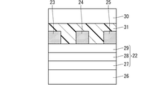
- Dissimilar material substrate removal process In the dissimilar material substrate removing step, first, the support substrate 30 is attached to the nitride semiconductor layer 22 or above the nitride semiconductor element 111 on the dissimilar material substrate 26, and then the dissimilar material substrate 26 is removed.
- the thickness of the nitride semiconductor layer 22, the source electrode 23, the drain electrode 24, and the gate electrode 25 is, for example, several ⁇ m to several tens of ⁇ m, respectively, as compared with the thickness of the dissimilar material substrate 26 (for example, 100 ⁇ m to 800 ⁇ m). Thin. Therefore, when the dissimilar material substrate 26 is removed from below the nitride semiconductor element 111, it is difficult to maintain the fine shape of the nitride semiconductor element 111 without deformation as it is. Therefore, when removing the dissimilar material substrate 26, it is necessary to attach the support substrate 30 to the nitride semiconductor element 111.
- FIG. 8 is a schematic cross-sectional view of a structure in which the support substrate 30 is attached to the nitride semiconductor element 111 on the dissimilar material substrate 26.
- the support substrate 30 has high flatness and chemical resistance, such as Si wafer and quartz glass.
- the support substrate 30 is attached to the nitride semiconductor element 111 using an organic adhesive 31 or the like. Since the nitride semiconductor element 111 and the support substrate 30 need to be finally separated, the adhesive 31 is preferably one that can be peeled off by, for example, solution treatment such as a stripping solution, heat treatment, or ultraviolet irradiation. Is.
- FIG. 9 shows a state in which the dissimilar material substrate 26 is removed from below the nitride semiconductor element 111 after the support substrate 30 is attached to the nitride semiconductor element 111 on the dissimilar material substrate 26 with an adhesive 31.
- the dissimilar material substrate 26 is removed by a polishing process using a mechanical polishing method or the like.
- a part of the buffer layer 27 may be removed by the polishing treatment.
- the surface 27a of the buffer layer 27, which appears after removing the dissimilar material substrate 26 from below the nitride semiconductor element 111 by polishing, is finally finished by the CMP method.
- the surface 4a of the diamond substrate 4 after the flattening step and the surface 27a of the buffer layer 27 after the dissimilar material substrate removing step both have high flatness. ing. Therefore, a high bonding area ratio can be obtained by direct bonding of both.
- a high bonding area ratio can be obtained by direct bonding of both.
- an intermolecular force such as van der Waals force. Or, physical joining occurs due to the anchor effect.
- the direct bonding step be performed in a clean environment such as in a vacuum in order to prevent organic substances floating in the atmosphere and impurities from the outside from being mixed into the bonding surface.
- the support substrate 30 is separated from the nitride semiconductor element 111 by a solution treatment such as a stripping solution, a heat treatment, or irradiation with ultraviolet rays as described above, so that the nitride semiconductor element 111 is directly mounted on the diamond substrate 4.
- the bonded semiconductor device 110 is obtained.
- the surface 4a of the diamond substrate 4 is processed and flattened by using the diamond processing method according to the first embodiment to have a flat surface 4a.
- the diamond substrate 4 is manufactured.
- ⁇ A-3. Effect> The effect described in is obtained.
- the diamond substrate 4 manufactured by the method for manufacturing a diamond substrate according to the present embodiment is prepared through a flattening step, and the surface on which the nitride semiconductor layer 22 is exposed is exposed.
- the nitride semiconductor element 111 which is a material having 27a, is prepared through the nitride semiconductor element forming step and the dissimilar material substrate removing step, and the surface 27a on which the nitride semiconductor layer 22 is exposed and the diamond processing method according to the first embodiment are prepared. Is directly joined to the surface 4a flattened using.
- the diamond substrate 4 functions as a heat diffusion layer for removing heat generated by the nitride semiconductor element 111 due to its high thermal conductivity.
- the heat generated by the nitride semiconductor element 111 is effectively transferred to the diamond substrate 4. be able to. As a result, it is possible to improve the problem that the degree of temperature rise is suppressed during the high output operation of the nitride semiconductor element 111 and the output power is lowered due to the temperature rise.
- the semiconductor device 110 has been further processed such that wires and lead wires are attached to the source electrodes 23, the drain electrodes 24, and the gate electrodes 25, and the semiconductor device 110 is sealed with a resin. It may be a thing.
- the nitride semiconductor element 111 is formed first, and then the surface 27a of the nitride semiconductor element 111 and the surface 4a of the diamond substrate 4 are directly bonded.
- the nitride semiconductor element 111 is formed on the dissimilar material substrate 26.
- the dissimilar material substrate 26 is removed in a state where a part, for example, the nitride semiconductor layer 22 is formed, and the surface 27a of the nitride semiconductor layer 22 and the surface 4a of the diamond substrate 4 are directly bonded, and then the nitride semiconductor layer 22 is formed.
- Each electrode of the source electrode 23, the drain electrode 24, and the gate electrode 25 may be provided on the surface of the above.
- the semiconductor device in which the surface of the diamond substrate 4 and the surface of the nitride semiconductor element 111 are directly bonded has been described, but the nitride semiconductor element 111 may be used with another semiconductor element, for example. It may be a semiconductor element such as silicon or silicon carbide.
- the surface 4a of the diamond substrate 4 is processed and flattened by using the diamond processing method according to the first embodiment to manufacture a diamond substrate 4 having a flat surface 4a. do.
- the diamond processing method according to the first embodiment ⁇ A-3. Effect> The effect described in is obtained.
- the diamond substrate 4 manufactured by the method for manufacturing a diamond substrate according to the present embodiment is prepared, and the surface 27a on which the nitride semiconductor layer 22 as a semiconductor layer is exposed is exposed.
- a nitride semiconductor element 111, which is a material to be possessed, is prepared, and the surface 27a on which the nitride semiconductor layer 22 is exposed is directly bonded to the surface 4a flattened by the diamond processing method according to the first embodiment. ..
- the semiconductor device 110 manufactured by the method for manufacturing the semiconductor device according to the present embodiment there is a problem that the degree of temperature rise is suppressed during the high output operation of the nitride semiconductor element 111, and the output power is lowered due to the temperature rise. Can be improved.
Landscapes
- Chemical & Material Sciences (AREA)
- Organic Chemistry (AREA)
- Engineering & Computer Science (AREA)
- Metallurgy (AREA)
- Crystallography & Structural Chemistry (AREA)
- Materials Engineering (AREA)
- Physics & Mathematics (AREA)
- Plasma & Fusion (AREA)
- Thermal Sciences (AREA)
- Life Sciences & Earth Sciences (AREA)
- General Life Sciences & Earth Sciences (AREA)
- Geology (AREA)
- Inorganic Chemistry (AREA)
- Crystals, And After-Treatments Of Crystals (AREA)
- Drying Of Semiconductors (AREA)
Abstract
プラズマを用いてダイヤモンドを加工する方法において高い加工速度でダイヤモンドを加工できるダイヤモンドの加工方法を提供する。そのために、本開示の一態様のダイヤモンドの加工方法は、プラズマを用いてダイヤモンドの表面を加工するダイヤモンドの加工方法であって、プラズマを用いてダイヤモンドの表面を加熱し、ダイヤモンドの表面をグラファイト化してからグラファイトを昇華させる、ダイヤモンドの加工方法、である。
Description
本開示は、ダイヤモンドの加工方法、ダイヤモンド基板の製造方法、および半導体装置の製造方法に関する。
ダイヤモンドは、材料中で最も高い熱伝導率等の優れた性質を持ち、例えばダイヤモンド基板を半導体装置の放熱のために用いる等の、様々な応用が考えられている。そのような応用のためにはダイヤモンドを必要に応じ加工する必要があるが、ダイヤモンドは材料中で最も高い硬度を有しているため、その加工処理は容易ではない。
従来から、単結晶及び多結晶ダイヤモンドの表面形状を加工するための種々の方法が検討されている。同じダイヤモンドなど硬質の粒子を研磨盤に用いて機械的に研磨する機械研磨法や、微粒子を含む研磨剤を用いる化学機械研磨(CMP:Chemical Mechanical Polishing)法などの他、プラズマを利用してエッチングを行う加工方法が知られている(例えば、特許文献1参照)。
しかしながら、特許文献1の加工方法の加工速度は十分ではなく、より高い加工速度でダイヤモンドを加工できることが望ましく、例えばより高い加工速度でダイヤモンド基板を加工してダイヤモンド基板を製造できることが、ダイヤモンド基板を半導体装置に用いる上で望ましい。
本開示は、上記のような課題を解決するためになされたものであり、プラズマを用いてダイヤモンドを加工する方法において高い加工速度でダイヤモンドを加工できるダイヤモンドの加工方法と、当該ダイヤモンドの加工方法を用いたダイヤモンド基板の製造方法と、当該ダイヤモンド基板の製造方法を用いた半導体装置の製造方法と、を提供することを目的とする。
本開示の一態様のダイヤモンドの加工方法は、プラズマを用いてダイヤモンドの表面を加工するダイヤモンドの加工方法であって、プラズマを用いてダイヤモンドの表面を加熱し、ダイヤモンドの表面をグラファイト化してからグラファイトを昇華させる、ダイヤモンドの加工方法、である。
また、本開示の別の一態様のダイヤモンドの加工方法は、プラズマを用いてダイヤモンドの表面を加工するダイヤモンドの加工方法であって、プラズマを用いてダイヤモンドの表面を加熱し、ダイヤモンドの表面の温度を3700K以上とする、ダイヤモンドの加工方法、である。
また、本開示のさらに別の一態様のダイヤモンドの加工方法は、プラズマを用いてダイヤモンドの表面を加工するダイヤモンドの加工方法であって、プラズマのガス温度は3700K以上であり、プラズマを用いてダイヤモンドの表面を加熱する、ダイヤモンドの加工方法、である。
また、本開示のダイヤモンド基板の製造方法は、ダイヤモンドが露出した表面を有するダイヤモンド基板を準備し、本開示のダイヤモンドの加工方法によりダイヤモンドが露出した表面を加工する、ダイヤモンド基板の製造方法、である。
また、本開示の半導体装置の製造方法は、本開示のダイヤモンド基板の製造方法により製造されたダイヤモンド基板を準備し、半導体層が露出した表面を有する材料を準備し、半導体層が露出した表面と、ダイヤモンドの加工方法により加工されたダイヤモンドが露出した表面と、を直接接合する、半導体装置の製造方法、である。
本開示の一態様のダイヤモンドの加工方法は、プラズマを用いてダイヤモンドの表面を加工するダイヤモンドの加工方法であって、プラズマを用いてダイヤモンドの表面を加熱し、ダイヤモンドの表面をグラファイト化してからグラファイトを昇華させる、ダイヤモンドの加工方法、である。これにより、プラズマを用いてダイヤモンドを加工する方法において高い加工速度でダイヤモンドを加工できるダイヤモンドの加工方法が提供される。
また、本開示の別の一態様のダイヤモンドの加工方法は、プラズマを用いてダイヤモンドの表面を加工するダイヤモンドの加工方法であって、プラズマを用いてダイヤモンドの表面を加熱し、ダイヤモンドの表面の温度を3700K以上とする、ダイヤモンドの加工方法、である。これにより、プラズマを用いてダイヤモンドを加工する方法において高い加工速度でダイヤモンドを加工できるダイヤモンドの加工方法が提供される。
また、本開示のさらに別の一態様のダイヤモンドの加工方法は、プラズマを用いてダイヤモンドの表面を加工するダイヤモンドの加工方法であって、プラズマのガス温度は3700K以上であり、プラズマを用いてダイヤモンドの表面を加熱する、ダイヤモンドの加工方法、である。これにより、プラズマを用いてダイヤモンドを加工する方法において高い加工速度でダイヤモンドを加工できるダイヤモンドの加工方法が提供される。
また、本開示のダイヤモンド基板の製造方法は、ダイヤモンドが露出した表面を有するダイヤモンド基板を準備し、本開示のダイヤモンドの加工方法によりダイヤモンドが露出した表面を加工する、ダイヤモンド基板の製造方法、である。これにより、プラズマを用いてダイヤモンドを加工する方法において高い加工速度でダイヤモンドを加工できるダイヤモンドの加工方法を用いたダイヤモンド基板の製造方法が提供される。
また、本開示の半導体装置の製造方法は、本開示のダイヤモンド基板の製造方法により製造されたダイヤモンド基板を準備し、半導体層が露出した表面を有する材料を準備し、半導体層が露出した表面と、ダイヤモンドの加工方法により加工されたダイヤモンドが露出した表面と、を直接接合する、半導体装置の製造方法、である。これにより、プラズマを用いてダイヤモンドを加工する方法において高い加工速度でダイヤモンドを加工できるダイヤモンドの加工方法を用いたダイヤモンド基板の製造方法、を用いた半導体装置の製造方法が提供される。
また、本願明細書に開示される技術に関連する目的と、特徴と、局面と、利点とは、以下に示される詳細な説明と添付図面とによって、さらに明白となる。
<A.実施の形態1>
<A-1.装置構成>
図1は、本実施の形態のダイヤモンドの加工方法を実施するために用いるドライエッチング装置の例であるドライエッチング装置100の概略構成図である。
<A-1.装置構成>
図1は、本実施の形態のダイヤモンドの加工方法を実施するために用いるドライエッチング装置の例であるドライエッチング装置100の概略構成図である。
図1に示されるように、ドライエッチング装置100は、プラズマ発生器101と、処理容器10と、ステージ14と、ガス供給部102と、排気部103と、を備える。
図1には、エッチングする対象物の例であるダイヤモンド基板4も示されている。ダイヤモンド基板4はダイヤモンドが露出した表面4aを有し、ドライエッチング装置100により表面4aがエッチングされ加工される(図2参照)。
プラズマ発生器101は、高周波電源1と、高周波電源1から投入された電力を伝播させる機能を備える導波管2と、プラズマ電極3と、を備える。高周波電源1と、導波管2と、プラズマ電極3と、は、投入された電力の伝播損失を出来る限り低く抑えるために、直接的に接続されていることが望ましい。但し、例えば、高周波電源1と導波管2との間を比較的電力損失の低い同軸ケーブルを介して接続してもよい。
高周波電源1には、プラズマを発生させるためのマイクロ波帯域の周波数で発振可能なものを用いる。マイクロ波の発振方式には、主にマグネトロン発振式と半導体発振式の二種類があり、最大投入電力が約1kW以上の高周波電源に対しては、マグネトロン発振式が一般的に用いられる。一方、半導体発振式の電源は、マグネトロン発振式で電力を安定的に供給することが難しい100W以下のような低電力領域や、狭帯域幅の発振周波数を利用する場合に用いられる。高周波電源1は、どちらの発振方式を用いるものであってもよい。
導波管2は、高周波電源1から投入されたマイクロ波の電力を、導波管2に差し込まれたプラズマ電極3を介し、プラズマ電極3とダイヤモンド基板4との間で発生するプラズマまで低損失で伝播させる機能を備えている。
導波管2は、電力計測器5と、スリースタブチューナー6と、可動短絡器7と、方向性結合器8と、ダミーロード9と、を備える。
電力計測器5は、高周波電源1からの投入電力及び可動短絡器7からの反射電力をモニターする。
スリースタブチューナー6はマイクロ波の位相を制御する。導波管2は、スリースタブチューナー6の代わりにE/Hチューナーを備えていてもよい。
可動短絡器7はマイクロ波を反射して定在波を形成するためのものである。
方向性結合器8は、可動短絡器7に反射されたマイクロ波の電力が高周波電源1に入ることを防ぐために、高周波電源1の方向へ伝搬するマイクロ波の伝播方向を変える。
ダミーロード9は、方向性結合器8に伝播方向を変えられたマイクロ波を吸収して、そのエネルギーを熱に変換する。
プラズマ電極3は、導波管2を通して、その一端側が処理容器10内に挿入されている。プラズマ電極3は、導波管2を通っていることで、高周波電源1と電気的に接続されている。図2に示すように、プラズマ電極3はパイプ状の構造となっている。プラズマ電極3の処理容器10内に挿入されている側の先端部の端面には、エッチングに用いるガスを処理容器10内に導入するガス導入口16である細穴が形成されている。図2ではガス導入口16が1つの場合が示されているが、プラズマ電極3の先端部の端面に複数のガス導入口16が形成されていてもよい。
ガス供給部102は、ガスボンベ40と、流量制御器(MFC:Mass Flow Controller)11とを備え、ガスボンベ40に保存されているガスを、流量制御器11により流量を制御してプラズマ電極3に供給する。ガス供給部102よりプラズマ電極3に供給されたガスは、プラズマ電極3パイプ状の構造の内部を通り、ガス導入口16を通じて処理容器10内に導入される。ドライエッチング装置100においてダイヤモンド基板4のエッチング処理に用いられるガスは、例えば、ダイヤモンドと化学的に反応するガスであるエッチングガス、つまり、例えば水素ガスもしくは酸素ガスである。または、水素ガスもしくは酸素ガスに加えさらに希ガスを含むガスが用いられてもよい。
排気部103は、排気バルブ12と真空ポンプ13とを備える。処理容器10は、排気バルブ12を介して真空ポンプ13と接続されており、処理容器10内の残留ガスを低圧まで排気することができる。処理容器10内の圧力は、図示されない圧力計で計測される。真空ポンプ13の排気量を排気バルブ12で調整することで処理容器10内を目的とする圧力に制御することができる。
ステージ14は、試料ホルダー15を備える。ステージ14は、処理容器10内に設置されており、試料ホルダー15を介してダイヤモンド基板4を真空チャックにより固定できる機能を備えている。また、ステージ14は、加熱機構を備えており、試料ホルダー15上に固定されたダイヤモンド基板4を目的とする温度に加熱することができる。
さらに、図3に示すように、ステージ14は、可動機構を備える。ステージ14は、可動機構により、XYZ方向へ、またはXZ方向および回転方向へ動かされる。可動機構は外部装置によって制御される。ステージ14のZ方向の動きは、プラズマ電極3とダイヤモンド基板4との間の距離(ギャップ)W(図2を参照)の調整に用いられる。プラズマはプラズマ電極3の端面の面積に対応して局所的に発生するが、XY方向の動きもしくはX方向および回転方向の動きにより、プラズマをダイヤモンド基板4の表面4aを二次元的に走査させて大面積のダイヤモンド基板4をエッチングし加工できる。
ステージ14、処理容器10と、試料ホルダー15上に固定されたダイヤモンド基板4と、は、グランド電位に接続されている。
<A-2.ダイヤモンドの加工方法>
本実施の形態に係るダイヤモンドの加工方法およびその際に用いられるドライエッチング装置100の動作について説明する。
本実施の形態に係るダイヤモンドの加工方法およびその際に用いられるドライエッチング装置100の動作について説明する。
本実施の形態に係るダイヤモンドの加工方法で平坦化加工を行う対象のダイヤモンド基板4は、単結晶ダイヤモンド基板または多結晶ダイヤモンド基板のいずれでもよい。多結晶ダイヤモンド基板は、異種材料の母材ウエハ、例えば、シリコン(Si)、炭化ケイ素(SiC)、サファイヤ(Al2O3)などの上にCVD法により多結晶ダイヤモンド膜を形成することで作製することができるため、単結晶に比べて、安価且つ大面積化が容易といった観点から、例えば実施の形態3で説明する窒化物半導体装置の基板としてより好適である。しかし、多結晶ダイヤモンド基板においては、結晶粒の成長に対応した膜厚の増加にともなって、表面に数μmから数十μmの荒れた凹凸形状が形成される。そのため、単結晶ダイヤモンド基板と比べ、多結晶ダイヤモンド基板の平坦化には、より高い加工速度と加工精度の両方が必要である。また、結晶粒間の配向性が不規則であり、各結晶面に対して加工速度が異なることから、平坦化がより難しい。
本実施の形態のダイヤモンドの加工方法を実行するにあたって、まず、ダイヤモンド基板4を処理容器10内の試料ホルダー15上に真空チャックで固定し、真空ポンプ13により処理容器10内を低圧まで排気する。
次に、ステージ14をZ方向に移動させ、プラズマ電極3とダイヤモンド基板4とのギャップWを調整する。
次に、プラズマ電極3端面のガス導入口16からエッチング処理に用いるガスを処理容器10内に導入する。このとき、排気バルブ12を調整して処理容器10内を準大気圧から大気圧程度の処理圧力、例えば65hPa以上2000hPa以下に設定する。
その後、ステージ14の加熱機構によってダイヤモンド基板4を加熱し、最後に、高周波電源1からマイクロ波電力を投入して、スリースタブチューナー6(もしくはE/Hチューナー)と可動短絡器7を用いて、導波管2の伝播経路でマイクロ波のインピーダンス整合を取り、プラズマPLを発生させてエッチング処理を行う。そして、図3に示すように、プラズマ発生中にステージ14をXY方向に、もしくはX方向および回転方向に動かして走査し、プラズマPLが照射されている領域であるプラズマ照射領域がダイヤモンド基板4の表面4a全体をスキャンすることによって平坦化加工が行われる。
ここで、上記のエッチング処理において、プラズマPL中に生成された活性種の照射領域におけるダイヤモンド基板4の表面4aの温度が、グラファイトが昇華する温度となるようプラズマ発生条件(投入電力、ガス圧、ギャップ距離、ガス供給量、希ガスのガス種及び添加量など)を調整する。グラファイトは約3700K以上で十分速く昇華し、このような温度では、ダイヤモンドの表面では、ダイヤモンドの一部が炭化によってグラファイトに変化し当該グラファイトが昇華する反応が起こる。この昇華反応は、活性種とダイヤモンドとの化学的なエッチング反応と併せて同時に進行するため、ダイヤモンドの加工速度を高める効果が期待できる。
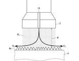
プラズマを発生させるにあっては、ステージ14を動かし、ギャップW(図2参照)を3mm以下に設定する。つまり、プラズマ電極3をダイヤモンド基板4の表面4aとの距離が3mm以下となるようにダイヤモンドの表面に対向させ、プラズマ電極3に電力を供給してプラズマPLを発生させる。このような狭ギャップWは、高圧雰囲気中で安定したプラズマ放電を維持するために望ましい。また、プラズマPLが狭ギャップ間に集中して発生するため、プラズマPLの発生している領域における単位体積当たりに与えられるマイクロ波の投入電力密度が非常に高くなる。これはプラズマPL中に生成される活性種の密度を著しく高める。実際に、パイプ状のプラズマ電極と単結晶Si基板との距離が0.3mmの狭ギャップ間で、65hPa~160hPa程度の準大気圧における水素ガス雰囲気中で発生させたプラズマにおいて、投入電力密度は約104W/cm3以上となり、プラズマ中に生成した活性種(原子状水素)密度は、約1017cm-3以上と非常に高密度であることが判明している。
このように、本実施の形態に係るダイヤモンドの加工方法においては、高圧雰囲気において狭ギャップW間で局所的に高い投入電力密度でプラズマPLを発生させるため、プラズマPL中に水素もしくは酸素の活性種を高密度に生成することが可能である。さらに、これらエッチングガス分子よりも質量の大きい希ガスを混合することで、希ガス原子のイオンやラジカルとの非弾性衝突によるエッチングガス分子の電離、励起、解離反応が促進され、プラズマPL中の活性種の密度をより高めることができる。
このようなプラズマPL中の活性種密度の増加は、プラズマPLのガス温度を著しく上昇させる。特に、ガス温度と電子温度がほぼ等しいようなプラズマを、熱平衡プラズマもしくは熱プラズマと呼ぶが、上記のようにガス温度を上げることで、プラズマPLを熱平衡プラズマとすることができる。例えば、水素分子と酸素分子は解離エネルギーが互いに近いが、どちらも大気圧で約4000Kまでガス温度が上昇する。さらに、希ガスのアルゴンでは、大気圧において数パーセントの電離で約10000Kまで上昇することが知られている。このような高温のガス温度を有する活性種がダイヤモンドに照射される場合、その照射領域の表面温度は、ガス温度とほぼ等しくなり、ダイヤモンドの一部が炭化してグラファイトに変化する。また、このような温度では、プラズマ照射表面では、ダイヤモンドの炭化と昇華反応が起こることになる。したがって、プラズマPLにより加熱されたダイヤモンド基板4の表面4aでは、高密度に生成された活性種との化学的な反応と、表面温度の上昇による昇華反応の、二つの反応が同時に起こることで、ダイヤモンドを高速でエッチング加工できる効果を得ることができる。
このようにダイヤモンド基板4の表面4aをグラファイト化してからグラファイトを昇華させるために、本実施の形態のダイヤモンドの加工方法では、プラズマPLを用いてダイヤモンド基板4の表面4aを加熱し、ダイヤモンド基板4の表面温度を例えば3700K以上とする。これにより、ダイヤモンド基板4の表面4aをグラファイト化してから昇華させ、例えば上記のように数μmから数十μmの荒れた凹凸形状を平坦化する速度を高めるのに十分な効果が得られる。ダイヤモンド基板4の表面4aの温度が上がるとグラファイトの昇華速度も上がり、温度を3700Kより高い例えば3800K以上とすることで、より高い昇華速度を実現できる。また、高温のガス温度を有する活性種がダイヤモンドに照射される場合、その照射領域の表面温度は、ガス温度とほぼ等しくなるため、プラズマPLのガス温度は目標とするダイヤモンド基板4の表面温度と同じであればよい。つまり、ダイヤモンド基板4の表面温度を3700K以上、または3800K以上とするためには、それぞれ、プラズマPLのガス温度を3700K以上、または3800K以上とすればよい。
ここで、プラズマ中のガス温度は、サハの電離式を用いて理論的に推定できることが知られている。例えば、Arイオン密度が約1016cm-3のとき、ガス温度は約10000Kと推定される。一方、プラズマ中に少量の窒素分子を混合し、その窒素分子ラジカルからの発光スペクトルを分析評価することで実験的にガス温度を見積もることも可能である。このとき、準大気圧から大気圧のような高圧条件の下では、窒素分子ラジカルの回転温度がガス温度とほぼ等しいとの仮定に基づいている。
また、本実施の形態に係るダイヤモンドの加工方法では、狭ギャップW間で局所的にプラズマを発生させるため、ダイヤモンド基板4の表面4aのプラズマ照射領域には高電界が印加される。この電界強度の分布は、ダイヤモンド基板4の表面形状に強く影響を受ける。例えば、ダイヤモンド基板4の表面4aの凹凸形状の凸部は、凹部に比べてプラズマ電極との距離が近いため電界が集中する。つまり、ダイヤモンド基板4の表面4aに電界を印加しつつプラズマPLをダイヤモンド基板4の表面4aに照射することで、ダイヤモンド基板4の表面4aの凸部の先端周辺の活性種密度は高くなり、プラズマPLの温度も上昇する。したがって、上記の反応により、ダイヤモンド基板4の表面4aの凸部は、凹部よりも優先的にエッチングが進行し、最終的に平坦な表面形状を得ることができる。また、この効果は、結晶粒間の配向性が無秩序な多結晶ダイヤモンドの表面形状の平坦化も可能にする。実際に、多結晶Si基板の表面形状は、プラズマ処理を施すことによって平均粗さRaで1nm以下まで平坦化することが判明している。
ここで、本実施の形態のダイヤモンドの加工方法で生成されるプラズマPLでは、低圧プラズマと比べてイオンやラジカルなど活性種の平均自由行程が非常に小さいため、スパッタリング現象のような物理的な効果はほとんど見られない。そのため、本実施の形態に係るダイヤモンドの加工方法では、高密度に生成された活性種による化学的な反応と表面温度の上昇による昇華反応とが支配的であり、高い加工速度の効果を小さいダメージで得ることが可能である。
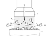
図2に示すように、本実施の形態のプラズマPLを用いたダイヤモンドの基板4の表面4aの加熱は、プラズマPLに新たなガスを供給しつつ行われる。プラズマPLを発生させる場合において、図2に示すようなプラズマ電極3のガス導入口16からのガス供給は、エッチング処理を行う上で重要な役割を担う。
一つは、プラズマPL中への不純物混入の防止効果である。プラズマPLの発生前、処理容器10内の残留ガスは、真空ポンプ13によって排気される。しかし、このときの到達真空度は、処理容器10の容積に対応した一般的なドライポンプやロータリーポンプを用いて排気可能な0.1Pa程度の圧力までで十分である。なぜなら、プラズマ電極3はガス導入口16の設けられている端面がダイヤモンド基板4に対向するように配置され、エッチング処理に用いられるガスは、プラズマ発生中に、プラズマ電極3端面のガス導入口16を通じて、プラズマPLへ直接導入される。このガス導入によって生じる狭ギャップW間のガス流れFLは、処理容器10内の残留ガスなどの不純物がプラズマPLの外部からプラズマPL中へと混入することを抑制する効果がある。したがって、プラズマPL中には、ガス導入口16から導入されたガス成分とダイヤモンド成分以外はほぼ存在しないことになり、純粋とみなせる環境下でエッチング処理が行われることになる。
プラズマ電極3のガス導入口16からのガス供給のもう一つの役割は、エッチング反応生成物の輸送である。先に述べたように、エッチングガスには、水素もしくは酸素が含まれる。プラズマPLを発生させるガス中に水素ガスが含まれる場合、水素の活性種とダイヤモンドが反応して、メタンのような揮発性の炭化水素化合物が生成される。また同様に酸素ガスが含まれる場合は、最終的に安定な一酸化炭素や二酸化炭素が生成される。しかし、図4に示すように、これらの反応生成物は、ガス流れFLによって速やかにプラズマPLの領域の外へ輸送される。この輸送機能には、エッチング反応生成物がプラズマPL中で分解・活性化することによって生じるダイヤモンド基板4表面への炭素化合物の付着・堆積による、加工速度の低下および表面粗さの増加を防ぐ効果がある。また、炭素化合物の付着・堆積現象は、ダイヤモンド基板4に対向するプラズマ電極3の表面においても同様に起こるため、これらをガス流れFLにより抑制することは、プラズマ放電の安定な維持に対して重要な役割を持つ。
以上をまとめると、本実施の形態のダイヤモンドの加工方法では、準大気圧から大気圧程度の高圧雰囲気のもと、プラズマ電極3とダイヤモンド基板4との狭ギャップW間で局所的に高い投入電力密度でプラズマPLを発生させることで、水素、酸素、もしくは希ガスの活性種が高密度に生成され、プラズマPL中のガス温度が著しく上昇する。このとき、活性種の照射領域の表面温度がグラファイトの昇華温度以上であるとき、ダイヤモンドの一部がグラファイトに変化して昇華する。したがって、高密度に生成された活性種との化学的な反応と昇華反応の二つの反応過程が同時に進行することによって、ダイヤモンド基板4の表面4aを高速でエッチング処理することができる。また、狭ギャップW間に高い電界強度が印加されることで、ダイヤモンド基板4の表面4aの凸部に対して電界集中が起こり、上記の反応によって、当該凸部が優先的にエッチングされる。これによって、ダイヤモンド基板4の表面4aを、実施の形態3で説明する窒化物半導体層との直接接合に必要な表面粗さに平坦化加工することができる。
上記の説明では本実施の形態のダイヤモンドの加工方法でダイヤモンド基板4のダイヤモンドが露出した表面4aを加工することを想定して説明したが、少なくとも一部にダイヤモンドを備え当該ダイヤモンドが露出した表面を持つ材料であれば、当該ダイヤモンドの当該表面を上記の説明同様に加工し当該表面を平坦化することができる。
<A-3.効果>
本実施の形態に係るダイヤモンドの加工方法は、プラズマPLを用いてダイヤモンドの表面を加工するダイヤモンドの加工方法であって、プラズマPLを用いてダイヤモンドの表面を加熱し、ダイヤモンドの表面をグラファイト化してから当該グラファイトを昇華させる、ダイヤモンドの加工方法である。これにより、高い加工速度でダイヤモンドの表面を加工できる。
本実施の形態に係るダイヤモンドの加工方法は、プラズマPLを用いてダイヤモンドの表面を加工するダイヤモンドの加工方法であって、プラズマPLを用いてダイヤモンドの表面を加熱し、ダイヤモンドの表面をグラファイト化してから当該グラファイトを昇華させる、ダイヤモンドの加工方法である。これにより、高い加工速度でダイヤモンドの表面を加工できる。
本実施の形態に係るダイヤモンドの加工方法は、プラズマPLを用いてダイヤモンドの表面を加工するダイヤモンドの加工方法であって、プラズマPLを用いてダイヤモンドの表面を加熱し、ダイヤモンドの表面の温度を3700K以上とする。これにより、高い加工速度でダイヤモンドの表面を加工できる。
本実施の形態に係るダイヤモンドの加工方法は、プラズマPLを用いてダイヤモンドの表面を加工するダイヤモンドの加工方法であって、プラズマPLを用いてダイヤモンドの表面を加熱し、ダイヤモンドの表面の温度をより望ましくは3800K以上とする。これにより、より高い加工速度でダイヤモンドの表面を加工できる。
本実施の形態に係るダイヤモンドの加工方法は、プラズマPLを用いてダイヤモンドの表面を加工するダイヤモンドの加工方法であって、プラズマPLのガス温度は3700K以上であり、プラズマPLを用いてダイヤモンドの表面を加熱する。これにより、高い加工速度でダイヤモンドの表面を加工できる。
本実施の形態に係るダイヤモンドの加工方法は、プラズマPLを用いてダイヤモンドの表面を加工するダイヤモンドの加工方法であって、プラズマPLのガス温度はより望ましくは3800K以上であり、プラズマPLを用いてダイヤモンドの表面を加熱する。これにより、より高い加工速度でダイヤモンドの表面を加工できる。
本実施の形態に係るダイヤモンドの加工方法において、プラズマPLの圧力は65hPa以上2000hPa以下である。これにより、プラズマPLのガス温度を3700K以上とし、またはダイヤモンドの表面の温度を3700K以上とし、またはダイヤモンドの表面をグラファイト化してから当該グラファイトを昇華させることがより容易になる。
プラズマPLは、エッチングガスを含むガスのプラズマである。これにより、プラズマ中に生成された活性種による化学的なエッチング反応により、より高い加工速度でダイヤモンドの表面を加工できる。
プラズマPLは、希ガスをさらに含むガスのプラズマである。これにより、プラズマPL中に生成される活性種の密度と温度がより上昇し、より高い加工速度でダイヤモンドの表面を加工できる。
本実施の形態に係るダイヤモンドの加工方法では、プラズマ電極3を用い、プラズマ電極3をダイヤモンドの表面に対向させ、プラズマ電極3に電力を供給してプラズマPLを発生させる。これにより、プラズマPLへの投入電力密度が高くなり、活性種密度の増加およびガス温度の上昇を実現できる。また、ダイヤモンドの表面の凹凸をより効果的に平坦化できる。
本実施の形態に係るダイヤモンドの加工方法では、プラズマ電極3を用い、プラズマ電極3をダイヤモンドの表面との距離が3mm以下となるようにダイヤモンドの表面に対向させ、プラズマ電極3に電力を供給してプラズマPLを発生させる。これにより、プラズマPLへの投入電力密度が高くなり、活性種密度の増加およびガス温度の上昇を実現できる。また、ダイヤモンドの表面の凹凸をより効果的に平坦化できる。
本実施の形態に係るダイヤモンドの加工方法では、プラズマPLを用いたダイヤモンドの表面の加熱は、プラズマPLに新たなガスを供給しつつ行われる。これにより、ガス流れFLが生じ、ガス流れFLによる輸送機能によって、エッチング反応生成物による加工速度の低下、および、表面粗さの増加を抑制できる。また、プラズマ放電がより安定になる。
本実施の形態に係るダイヤモンドの加工方法では、プラズマPLを用いたダイヤモンドの表面の加熱は、ダイヤモンドの表面に電界を印加しつつプラズマPLをダイヤモンドの表面に照射して行われる。これにより、ダイヤモンドの表面の凹凸をより効果的に平坦化できる。
本実施の形態に係るダイヤモンドの加工方法では、可動機構を備えるステージ14にダイヤモンドを設置し、当該可動機構によりステージ14を動かして、プラズマPLをダイヤモンドの表面上を走査させる。これにより、局所的に発生するプラズマPLを用いて、大面積のダイヤモンドの表面の平坦化加工をできる。
<A-4.その他>
上記の説明では本実施の形態のダイヤモンドの加工方法でダイヤモンド基板4の表面を平坦化することを想定して説明したが、本実施の形態のダイヤモンドの加工方法は、表面を平坦化するのではなく、例えば表面の平坦性を維持して表面形状を加工することに用いられてもよい。
上記の説明では本実施の形態のダイヤモンドの加工方法でダイヤモンド基板4の表面を平坦化することを想定して説明したが、本実施の形態のダイヤモンドの加工方法は、表面を平坦化するのではなく、例えば表面の平坦性を維持して表面形状を加工することに用いられてもよい。
本実施の形態のダイヤモンドの加工方法では、ダイヤモンドの一部が炭化によってグラファイトに変化する。グラファイト化した部分は上で説明したように昇華するが、一部がグラファイトのまま残る可能性がある。その場合、ダイヤモンドがグラファイト化しない温度、例えば1200℃以下の温度でエッチングを行い、グラファイトのまま残った部分を取り除くことができる。ダイヤモンドの熱伝導度は高く、本実施の形態のダイヤモンドの加工方法でダイヤモンドがグラファイト化する温度以上となるのはプラズマPLが照射された表面の近傍のみであり、グラファイトのまま残った部分を取り除くためのエッチングを行う場合も短時間で実行できる。
<B.実施の形態2>
実施の形態2では、上記のドライエッチング装置100で発生したプラズマのガス温度の測定方法について説明する。なお、ドライエッチング装置100の構成は、実施の形態1と同様である。
実施の形態2では、上記のドライエッチング装置100で発生したプラズマのガス温度の測定方法について説明する。なお、ドライエッチング装置100の構成は、実施の形態1と同様である。
<B-1.構成>
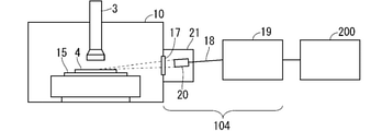
図5は、プラズマ発光分光測定系104の概略構成図を示している。プラズマ発光分光測定系104は、光ファイバー18と、分光器19と、光学レンズ20と、遮光板21と、を備える。また、分光器19によって測定された発光スペクトルを、例えばパーソナルコンピュータ200で分析することにより、ガス温度を測定できる。プラズマ発光分光測定系104およびパーソナルコンピュータ200は、ドライエッチング装置100の外部要素であってもよいし、ドライエッチング装置100が備えるものであってもよい。
図5は、プラズマ発光分光測定系104の概略構成図を示している。プラズマ発光分光測定系104は、光ファイバー18と、分光器19と、光学レンズ20と、遮光板21と、を備える。また、分光器19によって測定された発光スペクトルを、例えばパーソナルコンピュータ200で分析することにより、ガス温度を測定できる。プラズマ発光分光測定系104およびパーソナルコンピュータ200は、ドライエッチング装置100の外部要素であってもよいし、ドライエッチング装置100が備えるものであってもよい。
図1では省略されていたが、図5に示されるように、ドライエッチング装置100の処理容器10の側面には、プラズマの発した光を取り出すための窓が取り付けられている。
排気部103により低圧に設定された処理容器10の内部と外部との圧力差によって、窓には、歪を生じる。この歪は、プラズマの発した光が通過する際に影響を及ぼすことから、窓には光学窓(無歪窓)17を用いる。光学窓17は、光ファイバー18を介して分光器19と接続されており、分光器19はプラズマの発光スペクトルを取得できるようになっている。光学窓17に取り付けた光ファイバー18の先端部は、光学レンズ20を備えている。その光学レンズ20の焦点位置は、ダイヤモンド基板4の表面近傍であり、分光器19はダイヤモンド基板4の直上付近に発生するプラズマの発した光を取得する。また、光ファイバー18の先端部は、外部からの迷光が取り込まれることを防ぐために、遮光板21で覆われている。
プラズマの発光スペクトルは分光器19によって取得される。ガス温度の測定においては、例えば、窒素分子ラジカルからの第二正帯における発光輝線が利用されるため、分光器19は、例えば、測定波長が300nmから400nmの範囲を計測可能なものである。
<B-2.動作・作用>
プラズマのガス温度測定では、プラズマ中で生成した窒素分子ラジカルからの第二正帯における発光輝線を利用する。そのため、パイプ状のプラズマ電極3を通じて、処理容器10内に少量の窒素ガスを添加する。このとき、プラズマの発生条件は、エッチング条件と同じであり、窒素ガスの添加量は、エッチング時のプラズマ状態に影響を及ぼさない程度とする。
プラズマのガス温度測定では、プラズマ中で生成した窒素分子ラジカルからの第二正帯における発光輝線を利用する。そのため、パイプ状のプラズマ電極3を通じて、処理容器10内に少量の窒素ガスを添加する。このとき、プラズマの発生条件は、エッチング条件と同じであり、窒素ガスの添加量は、エッチング時のプラズマ状態に影響を及ぼさない程度とする。
次に、窒素ガスを混合したガスのプラズマの発光スペクトルを、光学窓17および光ファイバー18を通じて分光器19で取得する。得られた発光スペクトルに対して、300nmから400nmの波長範囲で計測した窒素の第二正帯におけるスペクトル構造と、理論計算結果との間でフィッティング解析を実行し、窒素分子ラジカルの回転温度を決定する。ここで、準大気圧や大気圧のような高圧条件、例えば65hPa以上2000hPa以下の圧力、において、上記のフィッティング解析により決定された回転温度は、一般に並進温度、すなわちガス温度とほぼ等しいと見なせることが分かっている。したがって、ダイヤモンド基板4の直上付近のプラズマ発光からガス温度を見積もることで、プラズマ照射中のダイヤモンドの表面温度を推定することができる。
ガス温度の評価方法には、他にも、原子状水素の発光スペクトルにおけるドップラー広がりを利用する方法や、水素分子のFulcher-α帯における発光スペクトルの構造を利用する方法もある。しかし、これらの方法を適用するには、上記の窒素ガスを利用したガス温度評価法と比べて、高い波長分解能を持つ分光器19が必要である。そのため、実施の形態1のダイヤモンドの加工方法では窒素を用いた測定方法を用いている。
<C.実施の形態3>
実施の形態3では、実施の形態1に係るダイヤモンドの加工方法を用いて表面を加工したダイヤモンド基板を用いて半導体装置を製造する、半導体装置の製造方法について説明する。
実施の形態3では、実施の形態1に係るダイヤモンドの加工方法を用いて表面を加工したダイヤモンド基板を用いて半導体装置を製造する、半導体装置の製造方法について説明する。
例えば窒化ガリウム(GaN)を用いた窒化物半導体素子は、高出力動作時の素子温度の上昇によって、GaNの物性から期待される本来の性能が十分に発揮できないことから、放熱技術の確立が求められている。このような窒化物半導体素子の放熱の課題を解決する方法の一つとして、材料中で最も高い熱伝導率を有するダイヤモンドを、半導体装置の基板に用いることが期待されている。しかし、ダイヤモンド基板上にデバイス品質の窒化物半導体層をエピタキシャル成長する技術は、まだ十分に確立されていない。そこで、他の方法として、窒化物半導体層とダイヤモンド基板との接合技術が検討されている。両者を直接接合するためには、接合面の形状を、不純物の混入なく、平均粗さRaで2nm以下まで平坦化することが望ましい。しかしながら、ダイヤモンドは材料中で最も高い硬度を有しているため、その加工処理は容易ではない。一方、異種材料もしくは同じ炭素材料から成る接着層(界面層)を挿入する接合方法も考えられるが、熱伝導率の観点から窒化物半導体層とダイヤモンド基板との直接接合がより理想的である。
そこで、本実施の形態に係るダイヤモンド基板の製造方法では、実施の形態1に係るダイヤモンドの加工方法を用いてダイヤモンド基板4の表面4aを加工して平坦化し、平坦な表面4aを持つダイヤモンド基板4を製造する。また、本実施の形態に係る半導体装置の製造方法では、本実施の形態に係るダイヤモンド基板の製造方法で製造されたダイヤモンド基板4を準備し、実施の形態1に係るダイヤモンドの加工方法を用いて平坦化された表面4aと、窒化物半導体層の表面と、を直接接合する。
なお、以下の説明において、本実施形態中に記載する「上方」、「下方」とは、構成要素の相対的位置関係を示す用語であり、半導体装置の製造時や使用時の配置における上下を制限するものではない。
<C-1.構成>
図6は、ダイヤモンド基板4を用いた半導体装置110の断面構造の模式図である。半導体装置110は、ダイヤモンド基板4と、窒化物半導体素子111と、を備える。
図6は、ダイヤモンド基板4を用いた半導体装置110の断面構造の模式図である。半導体装置110は、ダイヤモンド基板4と、窒化物半導体素子111と、を備える。
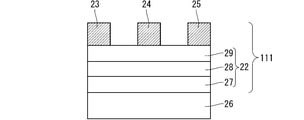
窒化物半導体素子111は、窒化物半導体層22と、窒化物半導体層22の表面上に設けられたソース電極23、ドレイン電極24、ゲート電極25の各電極と、を備える。窒化物半導体層22はダイヤモンド基板4の表面上に設けられている。
<C-2.製造方法>
半導体装置110を製造する方法である本実施の形態に係る半導体装置の製造方法は、大きく分けて次の4工程、すなわち、平坦化工程と、窒化物半導体素子形成工程と、異種材料基板除去工程と、直接接合工程と、を備える。
半導体装置110を製造する方法である本実施の形態に係る半導体装置の製造方法は、大きく分けて次の4工程、すなわち、平坦化工程と、窒化物半導体素子形成工程と、異種材料基板除去工程と、直接接合工程と、を備える。
平坦化工程は、実施の形態1に係るダイヤモンドの加工方法によりダイヤモンド基板4の表面を平坦化する工程であり、本実施の形態に係るダイヤモンド基板の製造方法で製造されたダイヤモンド基板4を準備する工程ともみなせる。
窒化物半導体素子形成工程は、SiCなどの異種材料基板26上に窒化物半導体素子111を形成する工程である。
異種材料基板除去工程は、窒化物半導体素子111の下方から異種材料基板26を除去する工程である。
直接接合工程は、実施の形態1に係るダイヤモンドの加工方法で加工された、もしくはダイヤモンド基板4と窒化物半導体素子111とを直接接合する工程である。
以下、上記の各工程について説明する。
<C-2-1.平坦化工程>
平坦化工程では、ダイヤモンドが露出した表面4aを有するダイヤモンド基板4を準備し、実施の形態1に係るダイヤモンドの加工方法により、表面4aをエッチングして加工し、平坦化する。つまり、本実施の形態に係るダイヤモンド基板の製造方法では、ダイヤモンドが露出した表面4aを有するダイヤモンド基板4を準備し、実施の形態1に係るダイヤモンドの加工方法により、表面4aをエッチングして加工し、平坦化する。
平坦化工程では、ダイヤモンドが露出した表面4aを有するダイヤモンド基板4を準備し、実施の形態1に係るダイヤモンドの加工方法により、表面4aをエッチングして加工し、平坦化する。つまり、本実施の形態に係るダイヤモンド基板の製造方法では、ダイヤモンドが露出した表面4aを有するダイヤモンド基板4を準備し、実施の形態1に係るダイヤモンドの加工方法により、表面4aをエッチングして加工し、平坦化する。
平坦化工程後の表面4a(図10参照)の粗さは、平均粗さRaで2nm以下に、より望ましくは平均粗さRaで1nm以下にする。実施の形態1に係るダイヤモンドの加工方法については、実施の形態1で説明済みであるため詳細は省略する。
<C-2-2.窒化物半導体素子形成工程>
図7は、異種材料基板26上に形成された窒化物半導体素子111の断面構造の模式図である。
図7は、異種材料基板26上に形成された窒化物半導体素子111の断面構造の模式図である。
異種材料基板26は、例えば、SiやSiCなどの単結晶基板である。
窒化物半導体層22の形成は、例えば有機金属気相成長法によって行われ、例えば、Ga原料にはトリメチルガリウム、アルミニウム(Al)原料はトリメチルアルミニウム、インジウム(In)原料はトリメチルインジウム、窒素(N)原料はアンモニアがそれぞれ用いられる。また、その他の窒化物半導体層22の形成方法には、分子線エピタキシー法などがある。
本実施の形態では、窒化物半導体層22は、異種材料基板26に近い側から順にバッファー層27(例えば、GaNまたはAlGaN)、チャネル層28(例えば、GaN)、バリア層29(例えば、AlGaNまたはInAlN)を備える。このように、窒化物半導体素子111はGaN半導体層であるチャネル層28を備える。窒化物半導体層22は、例えば、バッファー層27やチャネル層28が意図的な不純物の注入がされていない真性半導体層であるようなものでもよい。
バッファー層27は、異種材料基板26との間の格子不整合によって発生する歪を緩和するため、成長初期に低温形成した層を含んでもよい。また、バッファー層27中の欠陥を介した漏れ電流を抑制するため、成長中に鉄や炭素などの不純物を添加し、バッファー層27を高抵抗化してもよい。
チャネル層28とバリア層29とのヘテロ接合界面には、分極効果によって二次元電子ガス(2DEG、two dimensional electron gas)が誘起される。この2DEGは、ヘテロ接合界面近傍でシート状に形成され、高い電子密度(約1013cm-2)と高い電子移動度(約2000cm2/Vs)を示すことが知られており、窒化物半導体装置の主要なキャリアとして利用される。なお、チャネル層28とバリア層29との間にスペーサー層(例えば、AlNなど)を挿入し、2DEG密度の制御や、バリア層29を通じた漏れ電流の抑制などに利用してもよい。
異種材料基板26上に窒化物半導体層22が形成された後、窒化物半導体層22のバリア層29の上方に、ソース電極23と、ドレイン電極24と、ゲート電極25と、を形成する。これにより、図7に示されるように、異種材料基板26上に窒化物半導体素子111が形成された状態となる。
バリア層29の上方の各電極は、一般に金属材料によって形成される。ソース電極23とドレイン電極24には、例えば、チタンやAlなどが含まれる。この両電極と窒化物半導体層22との間の電気的な接触抵抗は、小さいことが望ましい。そのため、バリア層29のうち電極形成領域の下方の部分に、例えば、Siなどの不純物を添加し、N型の導電型に変えてもよい。ゲート電極25の材料には、例えば、ニッケルや白金などの金属材料、もしくは高濃度に不純物を添加してN型やP型の導電型を示す多結晶Siなどを用いる。
<C-2-3.異種材料基板除去工程>
異種材料基板除去工程では、まず、異種材料基板26上の窒化物半導体素子111の窒化物半導体層22や上方に、支持基板30を取り付け、その後、異種材料基板26を除去する。
異種材料基板除去工程では、まず、異種材料基板26上の窒化物半導体素子111の窒化物半導体層22や上方に、支持基板30を取り付け、その後、異種材料基板26を除去する。
窒化物半導体層22、およびソース電極23、ドレイン電極24、ゲート電極25の厚さは、それぞれ例えば数μmから数十μmであり、異種材料基板26の厚さ(例えば、100μm~800μm)と比べて薄い。そのため、窒化物半導体素子111の下方から異種材料基板26を除去したとき、そのままでは窒化物半導体素子111の微細な形状を変形なしに維持することが困難である。したがって、異種材料基板26を除去する際には、窒化物半導体素子111に支持基板30を取り付ける必要がある。
図8は、異種材料基板26上の窒化物半導体素子111に、支持基板30が取り付けられた構造の断面の模式図である。
支持基板30は、例えば、Siウエハや石英ガラスなど、平坦性が高く、耐薬品性があるものである。支持基板30は、有機系の接着剤31などを用いて窒化物半導体素子111に取り付けられる。窒化物半導体素子111と支持基板30とは最終的に分離される必要があるため、接着剤31は、例えば、剥離液などの溶液処理、加熱処理、または紫外線照射などで剥離可能なものが好適である。
図9は、異種材料基板26上の窒化物半導体素子111に、接着剤31により支持基板30を取り付けた後、窒化物半導体素子111の下方から異種材料基板26を除去した状態を示している。異種材料基板26は、機械研磨法などを用いた研磨加工によって除去される。このとき、研磨処理によってバッファー層27の一部が除去されても良い。研磨加工により窒化物半導体素子111の下方から異種材料基板26を除去して現れるバッファー層27の表面27aは、CMP法によって最終の仕上げ処理を行う。これによって、バッファー層27の表面27a(図10参照)にRaで2nm以下、より望ましくはRaで1nm以下の平坦な表面形状を形成することが可能である。
<C-2-4.直接接合工程>
直接接合工程では、図10に示されるように、平坦化工程で平坦化加工が施されたダイヤモンド基板4の表面4aと、窒化物半導体素子111の表面27aと、を直接接合する。
直接接合工程では、図10に示されるように、平坦化工程で平坦化加工が施されたダイヤモンド基板4の表面4aと、窒化物半導体素子111の表面27aと、を直接接合する。
平坦化工程と異種材料基板除去工程とで説明したように、平坦化工程後のダイヤモンド基板4の表面4aおよび異種材料基板除去工程後のバッファー層27の表面27aは、ともに高い平坦性を有している。そのため、両者の直接接合では、高い接合面積割合が得られる。その接合界面では、例えば、炭素、Ga、Nとの間の直接的な結合、もしくは、これら元素と酸素や水素を介した結合などの化学結合に加えて、ファンデルワールス力などの分子間力や、アンカー効果による物理的な接合などが生じる。直接接合工程は、大気中に浮遊する有機物や外部からの不純物などが接合面に混入することを防ぐために、真空中などのクリーンな環境下で行うことが望ましい。接合後は、上記のような剥離液などの溶液処理、加熱処理、または紫外線照射などにより支持基板30を窒化物半導体素子111から分離することで、ダイヤモンド基板4上に窒化物半導体素子111が直接接合された半導体装置110が得られる。
以上をまとめると、本実施の形態に係るダイヤモンド基板の製造方法では、実施の形態1に係るダイヤモンドの加工方法を用いてダイヤモンド基板4の表面4aを加工して平坦化し、平坦な表面4aを持つダイヤモンド基板4を製造する。実施の形態1に係るダイヤモンドの加工方法を用いることにより、ダイヤモンド基板4の製造時に、<A-3.効果>に記載の効果が得られる。
また、本実施の形態に係る半導体装置の製造方法では、本実施の形態に係るダイヤモンド基板の製造方法で製造されたダイヤモンド基板4を平坦化工程を通して準備し、窒化物半導体層22が露出した表面27aを有する材料である窒化物半導体素子111を窒化物半導体素子形成工程および異種材料基板除去工程を通して準備し、窒化物半導体層22が露出した表面27aと、実施の形態1に係るダイヤモンドの加工方法を用いて平坦化された表面4aと、を直接接合する。ダイヤモンド基板4は、高い熱伝導性により、窒化物半導体素子111で発生する熱を取り除くための熱拡散層として機能する。特に、本実施の形態では、ダイヤモンド基板4と窒化物半導体素子111のバッファー層27との間を直接接合しているため、窒化物半導体素子111で発生する熱を効果的にダイヤモンド基板4に伝えることができる。その結果、窒化物半導体素子111の高出力動作時に温度上昇度合いが抑制され、温度上昇により出力電力が低下する問題を改善することができる。
<C-3.その他>
半導体装置110は、図11に示される状態から、ソース電極23、ドレイン電極24、ゲート電極25の各電極にワイヤやリード線が取り付けられたり、樹脂により封止されたり等、さらに加工がされたものであってもよい。
半導体装置110は、図11に示される状態から、ソース電極23、ドレイン電極24、ゲート電極25の各電極にワイヤやリード線が取り付けられたり、樹脂により封止されたり等、さらに加工がされたものであってもよい。
実施の形態3では窒化物半導体素子111を先に形成してから窒化物半導体素子111の表面27aとダイヤモンド基板4の表面4aを直接接合したが、異種材料基板26上に窒化物半導体素子111の一部、例えば窒化物半導体層22までが形成された状態で異種材料基板26を取り除き、窒化物半導体層22の表面27aとダイヤモンド基板4の表面4aを直接接合し、その後、窒化物半導体層22の表面上にソース電極23、ドレイン電極24、ゲート電極25の各電極を設けるなどしてもよい。
また、実施の形態3ではこれまでダイヤモンド基板4の表面と、窒化物半導体素子111の表面と、が直接接合された半導体装置について説明してきたが、窒化物半導体素子111を他の半導体素子、例えばシリコンや炭化珪素等、の半導体素子としてもよい。
<C-4.効果>
本実施の形態に係るダイヤモンド基板の製造方法では、実施の形態1に係るダイヤモンドの加工方法を用いてダイヤモンド基板4の表面4aを加工して平坦化し、平坦な表面4aを持つダイヤモンド基板4を製造する。実施の形態1に係るダイヤモンドの加工方法を用いることにより、ダイヤモンド基板4の製造時に、<A-3.効果>に記載の効果が得られる。
本実施の形態に係るダイヤモンド基板の製造方法では、実施の形態1に係るダイヤモンドの加工方法を用いてダイヤモンド基板4の表面4aを加工して平坦化し、平坦な表面4aを持つダイヤモンド基板4を製造する。実施の形態1に係るダイヤモンドの加工方法を用いることにより、ダイヤモンド基板4の製造時に、<A-3.効果>に記載の効果が得られる。
本実施の形態に係る半導体装置の製造方法では、本実施の形態に係るダイヤモンド基板の製造方法で製造されたダイヤモンド基板4を準備し、半導体層である窒化物半導体層22が露出した表面27aを有する材料である窒化物半導体素子111を準備し、窒化物半導体層22が露出した表面27aと、実施の形態1に係るダイヤモンドの加工方法を用いて平坦化された表面4aと、を直接接合する。これにより、本実施の形態に係る半導体装置の製造方法で製造された半導体装置110では、窒化物半導体素子111の高出力動作時に温度上昇度合いが抑制され、温度上昇により出力電力が低下する問題を改善することができる。
なお、各実施の形態を自由に組み合わせたり、各実施の形態を適宜、変形、省略したりすることが可能である。
1 高周波電源、2 導波管、3 プラズマ電極、4 ダイヤモンド基板、4a 表面、5 電力計測器、6 スリースタブチューナー、7 可動短絡器、8 方向性結合器、9 ダミーロード、10 処理容器、11 流量制御器、12 排気バルブ、13 真空ポンプ、14 ステージ、15 試料ホルダー、16 ガス導入口、17 光学窓、18 光ファイバー、19 分光器、20 光学レンズ、21 遮光板、22 窒化物半導体層、23 ソース電極、24 ドレイン電極、25 ゲート電極、26 異種材料基板、27 バッファー層、27a 表面、28 チャネル層、29 バリア層、30 支持基板、31 接着剤、40 ガスボンベ、100 ドライエッチング装置、101 プラズマ発生器、102 ガス供給部、103 排気部、104 プラズマ発光分光測定系、110 半導体装置、111 窒化物半導体素子、200 パーソナルコンピュータ、PL プラズマ。
Claims (22)
- プラズマを用いてダイヤモンドの表面を加工するダイヤモンドの加工方法であって、
前記プラズマを用いて前記ダイヤモンドの前記表面を加熱し、前記ダイヤモンドの前記表面をグラファイト化してから前記グラファイトを昇華させる、
ダイヤモンドの加工方法。 - プラズマを用いてダイヤモンドの表面を加工するダイヤモンドの加工方法であって、
前記プラズマを用いて前記ダイヤモンドの前記表面を加熱し、前記ダイヤモンドの前記表面の温度を3700K以上とする、
ダイヤモンドの加工方法。 - 請求項2に記載のダイヤモンドの加工方法であって、
前記プラズマを用いて前記ダイヤモンドの前記表面を加熱し、前記ダイヤモンドの前記表面の前記温度を3800K以上とする、
ダイヤモンドの加工方法。 - プラズマを用いてダイヤモンドの表面を加工するダイヤモンドの加工方法であって、
前記プラズマのガス温度は3700K以上であり、
前記プラズマを用いて前記ダイヤモンドの前記表面を加熱する、
ダイヤモンドの加工方法。 - 請求項4に記載のダイヤモンドの加工方法であって、
前記プラズマの前記ガス温度は3800K以上である、
ダイヤモンドの加工方法。 - 請求項1から5のいずれかに記載のダイヤモンドの加工方法であって、
前記プラズマの圧力は65hPa以上2000hPa以下である、
ダイヤモンドの加工方法。 - 請求項1から6のいずれかに記載のダイヤモンドの加工方法であって、
前記プラズマは熱平衡プラズマである、
ダイヤモンドの加工方法。 - 請求項1から7のいずれかに記載のダイヤモンドの加工方法であって、
前記プラズマは、エッチングガスを含むガスのプラズマである、
ダイヤモンドの加工方法。 - 請求項8に記載のダイヤモンドの加工方法であって、
前記プラズマは、希ガスをさらに含むガスのプラズマである、
ダイヤモンドの加工方法。 - 請求項1から9のいずれかに記載のダイヤモンドの加工方法であって、
プラズマ電極を用い、前記プラズマ電極を前記ダイヤモンドの前記表面に対向させ、前記プラズマ電極を介して電力を供給して前記プラズマ電極と前記ダイヤモンドの間に前記プラズマを発生させる、
ダイヤモンドの加工方法。 - 請求項10に記載のダイヤモンドの加工方法であって、
前記プラズマ電極を用い、前記プラズマ電極を前記ダイヤモンドの前記表面との距離が3mm以下となるように前記ダイヤモンドの前記表面に対向させ、前記プラズマ電極を介して電力を供給して前記プラズマ電極と前記ダイヤモンドの間に前記プラズマを発生させる、
ダイヤモンドの加工方法。 - 請求項1から11のいずれかに記載のダイヤモンドの加工方法であって、
前記プラズマを用いた前記ダイヤモンドの前記表面の加熱は、前記プラズマに新たなガスを供給しつつ行われる、
ダイヤモンドの加工方法。 - 請求項1から12のいずれかに記載のダイヤモンドの加工方法であって、
前記プラズマを用いた前記ダイヤモンドの前記表面の加熱は、前記ダイヤモンドの前記表面に電界を印加しつつ前記プラズマを前記ダイヤモンドの前記表面に照射して行われる、
ダイヤモンドの加工方法。 - 請求項1から13のいずれかに記載のダイヤモンドの加工方法であって、
可動機構を備えるステージに前記ダイヤモンドを設置し、
前記可動機構により前記ステージを動かして、前記プラズマを前記ダイヤモンドの前記表面上を走査させる、
ダイヤモンドの加工方法。 - 請求項1から14のいずれかに記載のダイヤモンドの加工方法であって、
前記プラズマを用いて前記表面をエッチングする、
ダイヤモンドの加工方法。 - 請求項1から15のいずれかに記載のダイヤモンドの加工方法であって、
前記ダイヤモンドの加工方法により前記ダイヤモンドの前記表面を平坦化する、
ダイヤモンドの加工方法。 - 請求項1から16のいずれかに記載のダイヤモンドの加工方法であって、
前記ダイヤモンドの加工方法により、前記ダイヤモンドの前記表面の平均粗さRaを2.0nm以下とする
ダイヤモンドの加工方法。 - ダイヤモンドが露出した表面を有するダイヤモンド基板を準備し、
請求項1から17のいずれかのダイヤモンドの加工方法により前記ダイヤモンドが露出した前記表面を加工する、
ダイヤモンド基板の製造方法。 - 請求項18のダイヤモンド基板の製造方法により製造されたダイヤモンド基板を準備し、
半導体層が露出した表面を有する材料を準備し、
前記半導体層が露出した前記表面と、前記ダイヤモンドの加工方法により加工された前記ダイヤモンドが露出した前記表面と、を直接接合する、
半導体装置の製造方法。 - 請求項19に記載の半導体装置の製造方法であって、
前記半導体層は窒化物半導体層である、
半導体装置の製造方法。 - 請求項20に記載の半導体装置の製造方法であって、
前記材料は、窒化物半導体素子である、
半導体装置の製造方法。 - 請求項21に記載の半導体装置の製造方法であって、
前記窒化物半導体素子はGaN半導体層を備える、
半導体装置の製造方法。
Priority Applications (2)
| Application Number | Priority Date | Filing Date | Title |
|---|---|---|---|
| JP2020564780A JP6899977B1 (ja) | 2020-07-22 | 2020-07-22 | ダイヤモンドの加工方法、ダイヤモンド基板の製造方法、および半導体装置の製造方法 |
| PCT/JP2020/028448 WO2022018859A1 (ja) | 2020-07-22 | 2020-07-22 | ダイヤモンドの加工方法、ダイヤモンド基板の製造方法、および半導体装置の製造方法 |
Applications Claiming Priority (1)
| Application Number | Priority Date | Filing Date | Title |
|---|---|---|---|
| PCT/JP2020/028448 WO2022018859A1 (ja) | 2020-07-22 | 2020-07-22 | ダイヤモンドの加工方法、ダイヤモンド基板の製造方法、および半導体装置の製造方法 |
Publications (1)
| Publication Number | Publication Date |
|---|---|
| WO2022018859A1 true WO2022018859A1 (ja) | 2022-01-27 |
Family
ID=76650094
Family Applications (1)
| Application Number | Title | Priority Date | Filing Date |
|---|---|---|---|
| PCT/JP2020/028448 Ceased WO2022018859A1 (ja) | 2020-07-22 | 2020-07-22 | ダイヤモンドの加工方法、ダイヤモンド基板の製造方法、および半導体装置の製造方法 |
Country Status (2)
| Country | Link |
|---|---|
| JP (1) | JP6899977B1 (ja) |
| WO (1) | WO2022018859A1 (ja) |
Citations (4)
| Publication number | Priority date | Publication date | Assignee | Title |
|---|---|---|---|---|
| JP2004179014A (ja) * | 2002-11-28 | 2004-06-24 | Matsushita Electric Ind Co Ltd | プラズマ加工方法及び装置 |
| JP2007201029A (ja) * | 2006-01-25 | 2007-08-09 | National Institute Of Advanced Industrial & Technology | 炭素材料が被着した被処理物の清浄方法 |
| JP2008251893A (ja) * | 2007-03-30 | 2008-10-16 | Sharp Corp | Iii族窒化物半導体の加工方法、iii族窒化物半導体発光素子の製造方法、iii族窒化物半導体発光素子、iii族窒化物半導体レーザ素子の製造方法およびiii族窒化物半導体レーザ素子 |
| JP2019117880A (ja) * | 2017-12-27 | 2019-07-18 | 日亜化学工業株式会社 | 光源装置 |
Family Cites Families (1)
| Publication number | Priority date | Publication date | Assignee | Title |
|---|---|---|---|---|
| JP4599908B2 (ja) * | 2004-06-28 | 2010-12-15 | ブラザー工業株式会社 | Dlc被膜除去方法 |
-
2020
- 2020-07-22 JP JP2020564780A patent/JP6899977B1/ja active Active
- 2020-07-22 WO PCT/JP2020/028448 patent/WO2022018859A1/ja not_active Ceased
Patent Citations (4)
| Publication number | Priority date | Publication date | Assignee | Title |
|---|---|---|---|---|
| JP2004179014A (ja) * | 2002-11-28 | 2004-06-24 | Matsushita Electric Ind Co Ltd | プラズマ加工方法及び装置 |
| JP2007201029A (ja) * | 2006-01-25 | 2007-08-09 | National Institute Of Advanced Industrial & Technology | 炭素材料が被着した被処理物の清浄方法 |
| JP2008251893A (ja) * | 2007-03-30 | 2008-10-16 | Sharp Corp | Iii族窒化物半導体の加工方法、iii族窒化物半導体発光素子の製造方法、iii族窒化物半導体発光素子、iii族窒化物半導体レーザ素子の製造方法およびiii族窒化物半導体レーザ素子 |
| JP2019117880A (ja) * | 2017-12-27 | 2019-07-18 | 日亜化学工業株式会社 | 光源装置 |
Also Published As
| Publication number | Publication date |
|---|---|
| JP6899977B1 (ja) | 2021-07-07 |
| JPWO2022018859A1 (ja) | 2022-01-27 |
Similar Documents
| Publication | Publication Date | Title |
|---|---|---|
| CN102959140B (zh) | 外延膜形成方法、真空处理设备、半导体发光元件制造方法、半导体发光元件和照明装置 | |
| JP6078620B2 (ja) | ダイヤモンド上の窒化ガリウム型ウェーハ並びに製造設備及び製造方法 | |
| KR101564251B1 (ko) | 에피텍셜 막 형성방법, 스퍼터링 장치, 반도체 발광소자 제조방법, 반도체 발광소자, 및 조명장치 | |
| US10446468B2 (en) | Method of fabricating compound semiconductor device structures having polycrstalline CVD diamond | |
| CN101410549A (zh) | 微波等离子体cvd系统 | |
| US7628856B2 (en) | Method for producing substrate for single crystal diamond growth | |
| JP6947232B2 (ja) | 窒化ガリウム系膜ならびにその製造方法 | |
| KR101861709B1 (ko) | 플라즈마 식각 방법 | |
| CN116356280A (zh) | 一种微波等离子体化学气相沉积系统制备六方氮化硼薄膜的方法 | |
| US8715414B2 (en) | Process for producing Si(1-v-w-x)CwAlxNv base material, process for producing epitaxial wafer, Si(1-v-w-x)CwAlxNv base material, and epitaxial wafer | |
| JP6899977B1 (ja) | ダイヤモンドの加工方法、ダイヤモンド基板の製造方法、および半導体装置の製造方法 | |
| Guo et al. | Novel diamond and TaC composite coatings for efficient heat dissipation in GaN semiconductor devices | |
| KR100885690B1 (ko) | 다이아몬드막의 제조방법 및 다이아몬드막 | |
| Kato et al. | N-type doping on (001)-oriented diamond | |
| JP2019186474A (ja) | ボロン系膜の成膜方法および成膜装置 | |
| JP2019135739A (ja) | ボロン系膜の成膜方法および成膜装置 | |
| WO2017017858A1 (ja) | SiC基板の製造方法 | |
| JP5042134B2 (ja) | ダイヤモンド薄膜 | |
| JP2011021256A (ja) | ナノ結晶シリコン薄膜の成膜方法及びナノ結晶シリコン薄膜、並びに該薄膜を成膜する成膜装置 | |
| JPH0789793A (ja) | 高配向性ダイヤモンド薄膜の形成方法 | |
| JP2009070845A (ja) | 化合物半導体デバイスおよびその製造方法 | |
| JPH0649635B2 (ja) | ダイヤモンドの合成方法 | |
| Yasui et al. | Radio frequency power dependence of the characteristics of 3C-SiC on Si grown by triode plasma CVD using dimethylsilane | |
| JPH06321687A (ja) | 高配向性ダイヤモンド薄膜の形成方法 |
Legal Events
| Date | Code | Title | Description |
|---|---|---|---|
| ENP | Entry into the national phase |
Ref document number: 2020564780 Country of ref document: JP Kind code of ref document: A |
|
| 121 | Ep: the epo has been informed by wipo that ep was designated in this application |
Ref document number: 20945857 Country of ref document: EP Kind code of ref document: A1 |
|
| NENP | Non-entry into the national phase |
Ref country code: DE |
|
| 122 | Ep: pct application non-entry in european phase |
Ref document number: 20945857 Country of ref document: EP Kind code of ref document: A1 |