WO2022014392A1 - データ処理装置、データ処理システム、データ処理方法及びデータ処理プログラム - Google Patents
データ処理装置、データ処理システム、データ処理方法及びデータ処理プログラム Download PDFInfo
- Publication number
- WO2022014392A1 WO2022014392A1 PCT/JP2021/025335 JP2021025335W WO2022014392A1 WO 2022014392 A1 WO2022014392 A1 WO 2022014392A1 JP 2021025335 W JP2021025335 W JP 2021025335W WO 2022014392 A1 WO2022014392 A1 WO 2022014392A1
- Authority
- WO
- WIPO (PCT)
- Prior art keywords
- data
- processing
- wavelength
- data processing
- unit
- Prior art date
- Legal status (The legal status is an assumption and is not a legal conclusion. Google has not performed a legal analysis and makes no representation as to the accuracy of the status listed.)
- Ceased
Links
Images






Classifications
-
- G—PHYSICS
- G01—MEASURING; TESTING
- G01J—MEASUREMENT OF INTENSITY, VELOCITY, SPECTRAL CONTENT, POLARISATION, PHASE OR PULSE CHARACTERISTICS OF INFRARED, VISIBLE OR ULTRAVIOLET LIGHT; COLORIMETRY; RADIATION PYROMETRY
- G01J3/00—Spectrometry; Spectrophotometry; Monochromators; Measuring colours
- G01J3/28—Investigating the spectrum
- G01J3/443—Emission spectrometry
-
- H—ELECTRICITY
- H10—SEMICONDUCTOR DEVICES; ELECTRIC SOLID-STATE DEVICES NOT OTHERWISE PROVIDED FOR
- H10P—GENERIC PROCESSES OR APPARATUS FOR THE MANUFACTURE OR TREATMENT OF DEVICES COVERED BY CLASS H10
- H10P72/00—Handling or holding of wafers, substrates or devices during manufacture or treatment thereof
- H10P72/06—Apparatus for monitoring, sorting, marking, testing or measuring
- H10P72/0612—Production flow monitoring, e.g. for increasing throughput
-
- G—PHYSICS
- G01—MEASURING; TESTING
- G01N—INVESTIGATING OR ANALYSING MATERIALS BY DETERMINING THEIR CHEMICAL OR PHYSICAL PROPERTIES
- G01N21/00—Investigating or analysing materials by the use of optical means, i.e. using sub-millimetre waves, infrared, visible or ultraviolet light
- G01N21/84—Systems specially adapted for particular applications
- G01N21/88—Investigating the presence of flaws or contamination
- G01N21/95—Investigating the presence of flaws or contamination characterised by the material or shape of the object to be examined
- G01N21/9501—Semiconductor wafers
-
- G—PHYSICS
- G01—MEASURING; TESTING
- G01J—MEASUREMENT OF INTENSITY, VELOCITY, SPECTRAL CONTENT, POLARISATION, PHASE OR PULSE CHARACTERISTICS OF INFRARED, VISIBLE OR ULTRAVIOLET LIGHT; COLORIMETRY; RADIATION PYROMETRY
- G01J3/00—Spectrometry; Spectrophotometry; Monochromators; Measuring colours
- G01J3/28—Investigating the spectrum
-
- G—PHYSICS
- G06—COMPUTING OR CALCULATING; COUNTING
- G06N—COMPUTING ARRANGEMENTS BASED ON SPECIFIC COMPUTATIONAL MODELS
- G06N20/00—Machine learning
-
- G—PHYSICS
- G06—COMPUTING OR CALCULATING; COUNTING
- G06T—IMAGE DATA PROCESSING OR GENERATION, IN GENERAL
- G06T11/00—Two-dimensional [2D] image generation
- G06T11/10—Texturing; Colouring; Generation of textures or colours
-
- G—PHYSICS
- G06—COMPUTING OR CALCULATING; COUNTING
- G06T—IMAGE DATA PROCESSING OR GENERATION, IN GENERAL
- G06T7/00—Image analysis
- G06T7/0002—Inspection of images, e.g. flaw detection
- G06T7/0004—Industrial image inspection
-
- H—ELECTRICITY
- H10—SEMICONDUCTOR DEVICES; ELECTRIC SOLID-STATE DEVICES NOT OTHERWISE PROVIDED FOR
- H10P—GENERIC PROCESSES OR APPARATUS FOR THE MANUFACTURE OR TREATMENT OF DEVICES COVERED BY CLASS H10
- H10P72/00—Handling or holding of wafers, substrates or devices during manufacture or treatment thereof
- H10P72/06—Apparatus for monitoring, sorting, marking, testing or measuring
- H10P72/0604—Process monitoring, e.g. flow or thickness monitoring
-
- H—ELECTRICITY
- H10—SEMICONDUCTOR DEVICES; ELECTRIC SOLID-STATE DEVICES NOT OTHERWISE PROVIDED FOR
- H10P—GENERIC PROCESSES OR APPARATUS FOR THE MANUFACTURE OR TREATMENT OF DEVICES COVERED BY CLASS H10
- H10P72/00—Handling or holding of wafers, substrates or devices during manufacture or treatment thereof
- H10P72/06—Apparatus for monitoring, sorting, marking, testing or measuring
- H10P72/0614—Marking devices
-
- H—ELECTRICITY
- H10—SEMICONDUCTOR DEVICES; ELECTRIC SOLID-STATE DEVICES NOT OTHERWISE PROVIDED FOR
- H10P—GENERIC PROCESSES OR APPARATUS FOR THE MANUFACTURE OR TREATMENT OF DEVICES COVERED BY CLASS H10
- H10P95/00—Generic processes or apparatus for manufacture or treatments not covered by the other groups of this subclass
-
- G—PHYSICS
- G01—MEASURING; TESTING
- G01J—MEASUREMENT OF INTENSITY, VELOCITY, SPECTRAL CONTENT, POLARISATION, PHASE OR PULSE CHARACTERISTICS OF INFRARED, VISIBLE OR ULTRAVIOLET LIGHT; COLORIMETRY; RADIATION PYROMETRY
- G01J3/00—Spectrometry; Spectrophotometry; Monochromators; Measuring colours
- G01J3/28—Investigating the spectrum
- G01J2003/283—Investigating the spectrum computer-interfaced
- G01J2003/2833—Investigating the spectrum computer-interfaced and memorised spectra collection
-
- G—PHYSICS
- G06—COMPUTING OR CALCULATING; COUNTING
- G06T—IMAGE DATA PROCESSING OR GENERATION, IN GENERAL
- G06T2207/00—Indexing scheme for image analysis or image enhancement
- G06T2207/10—Image acquisition modality
- G06T2207/10024—Color image
-
- G—PHYSICS
- G06—COMPUTING OR CALCULATING; COUNTING
- G06T—IMAGE DATA PROCESSING OR GENERATION, IN GENERAL
- G06T2207/00—Indexing scheme for image analysis or image enhancement
- G06T2207/20—Special algorithmic details
- G06T2207/20081—Training; Learning
-
- G—PHYSICS
- G06—COMPUTING OR CALCULATING; COUNTING
- G06T—IMAGE DATA PROCESSING OR GENERATION, IN GENERAL
- G06T2207/00—Indexing scheme for image analysis or image enhancement
- G06T2207/30—Subject of image; Context of image processing
- G06T2207/30108—Industrial image inspection
- G06T2207/30148—Semiconductor; IC; Wafer
Definitions
- This disclosure relates to a data processing apparatus, a data processing system, a data processing method and a data processing program.
- the measurement data measured during the execution of the semiconductor manufacturing process for example, the measurement data measured by an emission spectroscopic analyzer, a mass analyzer, or the like (so-called multi-wavelength time-series data) generally has a high measurement resolution. , The amount of data is huge. Therefore, there is a management cost when managing the data. In addition, in the case of multi-wavelength time series data, it is difficult for the user to directly determine whether or not an abnormality has occurred.
- multi-wavelength time-series data is converted into an image and displayed, it is considered that the user can easily determine whether or not an abnormality has occurred. Furthermore, if the imaged data is compressed and managed, it is considered that the management cost can be suppressed.
- the present disclosure provides a data processing device, a data processing system, a data processing method, and a data processing program for compressing and imaging multi-wavelength time-series data while suppressing the loss of characteristic data.
- the data processing apparatus has, for example, the following configuration. That is, A pre-processing unit that generates normalized data by normalizing multi-wavelength time series data using predetermined reference data. An extraction unit that divides the normalized data into a plurality of regions for each predetermined time range and a predetermined wavelength range, and extracts outliers in each region as representative values. It has a generation unit that converts the representative value of each region into color data and generates image data.
- a data processing device for compressing and imaging multi-wavelength time-series data while suppressing the loss of characteristic data.
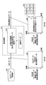
- FIG. 1 is a first diagram showing an example of a system configuration of a data processing system.
- FIG. 2 is a diagram showing an example of a semiconductor manufacturing process.
- FIG. 3 is a diagram showing an example of the hardware configuration of the data processing device.
- FIG. 4 is a diagram showing an example of OES data.
- FIG. 5 is a diagram showing a specific example of processing by the preprocessing unit.
- FIG. 6 is a diagram showing a specific example of processing by the compression unit.
- FIG. 7 is a diagram showing a specific example of image data.
- FIG. 8 is a flowchart showing the flow of the imaging process.
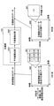
- FIG. 9A is a second diagram showing an example of the system configuration of the data processing system.
- FIG. 9A is a second diagram showing an example of the system configuration of the data processing system.
- FIG. 9B is a third diagram showing an example of a system configuration of a data processing system.
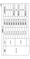
- FIG. 10 is a diagram showing an example of learning data.
- FIG. 11 is a diagram showing a specific example of the learning process by the learning unit.
- FIG. 12 is a diagram showing a specific example of inference processing by the inference unit.
- FIG. 13 is a flowchart showing the flow of abnormality detection processing.
- FIG. 14 is a fourth diagram showing an example of a system configuration of a data processing system.
- FIG. 1 is a first diagram showing an example of a system configuration of a data processing system.
- the data processing system 100 includes a semiconductor manufacturing process, an emission spectroscopic analyzer 140, and a data processing device 150.
- an object pre-processed wafer 110
- a result product processed wafer 130
- the pre-processed wafer 110 as used herein refers to a wafer (board) before being processed in the processing space 120
- the post-processed wafer 130 refers to a wafer (board) after being processed in the processing space 120. ..
- the emission spectroscopic analyzer 140 measures OES (Optical Emission Spectroscopy) data in the processing space 120 as the unprocessed wafer 110 is processed.
- OES Optical Emission Spectroscopy
- the OES data is "multi-wavelength time series data" including emission intensity data for each time, which is a number corresponding to the number of measurement wavelengths.
- the OES data measured by the emission spectroscopic analyzer 140 is stored in the OES data storage unit 155 of the data processing device 150.
- a data processing program is installed in the data processing device 150, and when the program is executed, the data processing device 150 serves as a preprocessing unit 151, a compression unit 152, an imaging unit 153, and a display control unit 154. Function.
- the pre-processing unit 151 reads OES data from the OES data storage unit 155 and performs pre-processing (for example, normalization processing) using predetermined reference data. Further, the pre-processing unit 151 notifies the compression unit 152 of the OES data after the pre-processing.
- pre-processing for example, normalization processing
- the compression unit 152 compresses the preprocessed OES data and notifies the imaging unit 153 of the compressed OES data. Specifically, the compression unit 152 divides the preprocessed OES data into a plurality of regions for each predetermined size (predetermined time range and predetermined wavelength range), and sets outliers included in each region in each region. By extracting as a representative value of, the OES data after preprocessing is compressed.
- the outliers refer to values that are statistically significantly different from other values in each region. In this way, by compressing the preprocessed OES data while leaving the outliers included in each region, it is possible to suppress the omission of the feature data (feature data indicating the occurrence of an abnormality) included in the OES data.
- the imaging unit 153 generates image data by converting the compressed OES data notified from the compression unit 152 into color data. Further, the imaging unit 153 stores the generated image data in the image data storage unit 156 and notifies the display control unit 154. As a result, the image data storage unit 156 stores the image data in which the amount of data is significantly reduced as compared with the OES data, and the management cost can be suppressed.
- the display control unit 154 controls to display the image data generated by the imaging unit 153 on a display device (not shown). As described above, since the image data generated by the imaging unit 153 is compressed, further processing is performed when displaying the image on the display device regardless of whether or not the number of pixels of the display device is limited. It can be displayed without doing it. That is, it is possible to avoid a situation in which, for example, image data is thinned out and feature data is lost when displaying on a display device.
- the user can visually determine whether or not an abnormality has occurred on the image data displayed on the display device. Can be done.
- FIG. 2 is a diagram showing an example of a semiconductor manufacturing process.
- the semiconductor manufacturing process 200 has a plurality of chambers which are an example of a processing space.
- the above-mentioned emission spectroscopic analyzer 140 is installed in each chamber, and OES data is measured in each chamber.
- OES data is measured in each chamber.
- the chamber 1 is the chamber A.
- the chamber A will be described as, for example, the chamber of the etching apparatus.
- FIG. 3 is a diagram showing an example of the hardware configuration of the data processing device.
- the data processing device 150 includes a CPU (Central Processing Unit) 301, a ROM (Read Only Memory) 302, and a RAM (Random Access Memory) 303. Further, the data processing device 150 has a GPU (Graphics Processing Unit) 304.
- a processor processing circuit, Processing Circuit, Processing Circuitry
- CPU 301 and GPU 304 and a memory such as ROM 302 and RAM 303 form a so-called computer.
- the data processing device 150 includes an auxiliary storage device 305, a display device 306, an operation device 307, an I / F (Interface) device 308, and a drive device 309.
- the hardware of the data processing device 150 is connected to each other via the bus 310.
- the CPU 301 is an arithmetic device that executes various programs (for example, a data processing program, etc.) installed in the auxiliary storage device 305.
- ROM 302 is a non-volatile memory and functions as a main storage device.
- the ROM 302 stores various programs, data, and the like necessary for the CPU 301 to execute various programs installed in the auxiliary storage device 305.
- the ROM 302 stores boot programs such as BIOS (Basic Input / Output System) and EFI (Extensible Firmware Interface).
- the RAM 303 is a volatile memory such as a DRAM (Dynamic Random Access Memory) or a SRAM (Static Random Access Memory), and functions as a main storage device.
- the RAM 303 provides a work area that is expanded when various programs installed in the auxiliary storage device 305 are executed by the CPU 301.
- the GPU 304 is an arithmetic device for image processing, and in the present embodiment, when the data processing program is executed by the CPU 301, the OES data is subjected to high-speed arithmetic by parallel processing.
- the GPU 304 is equipped with an internal memory (GPU memory), and temporarily holds information necessary for performing parallel processing on OES data.
- the auxiliary storage device 305 stores various programs, various data used when various programs are executed by the CPU 301, and the like.
- the OES data storage unit 155 and the image data storage unit 156 are realized in the auxiliary storage device 305.
- the display device 306 is, for example, a display device that displays image data generated by the imaging unit 153.
- the operation device 307 is an input device used by the user of the data processing device 150 to input various instructions to the data processing device 150.
- the I / F device 308 is a connection device for connecting to a network (not shown) and transmitting / receiving data to / from another device (for example, an emission spectroscopic analyzer).
- the drive device 309 is a device for setting the recording medium 320.
- the recording medium 320 referred to here includes a medium such as a CD-ROM, a flexible disk, a magneto-optical disk, or the like that optically, electrically, or magnetically records information. Further, the recording medium 320 may include a semiconductor memory or the like for electrically recording information such as a ROM or a flash memory.
- the various programs installed in the auxiliary storage device 305 are installed, for example, by setting the distributed recording medium 320 in the drive device 309 and reading the various programs recorded in the recording medium 320 by the drive device 309. Will be done.
- various programs installed in the auxiliary storage device 305 may be installed by being downloaded via a network (not shown).
- FIG. 4 is a diagram showing an example of OES data.
- the OES data 410 is for each time when each wavelength included in the wavelength range of visible light (200 [nm] to 800 [nm]) is measured in 0.5 [nm] increments. It is composed of a group of emission intensity data.
- the horizontal axis represents time and the vertical axis represents the emission intensity of each wavelength.
- the emission intensity data in the above is shown respectively.
- the time length of the OES data 410 is, for example, the processing time (for one wafer) in which the unprocessed wafer 110 is processed in the chamber A.
- the time length of the OES data 410 is, for example, the processing time of some of the processing steps when the unprocessed wafer 110 is processed in the chamber A under a plurality of processing steps. You may.
- the time length of the OES data 410 is, for example, when the unprocessed wafer 110 has a part of the processing steps executed by a plurality of recipes in the chamber A, the processing is executed by some of the recipes. It may be the time to be done.
- the OES data 420 shows how the emission intensity data of each point (each time, each wavelength) is arranged with the wavelength on the horizontal axis and the time on the vertical axis.
- 1201 points of emission intensity data are arranged in the horizontal axis direction.
- the sampling cycle of the emission intensity data is 0.1 seconds and the processing time (for one wafer) in which the unprocessed wafer 110 is processed in the chamber A is 300 seconds.
- 3000 points of emission intensity data are arranged in the vertical axis direction.
- the emission intensity data of each point of the OES data 420 is converted into color data and the generated image data is to be displayed on the display device 306, the number of pixels is 1201 pixels in the horizontal direction and 3000 pixels in the vertical direction. A display device is required.
- the OES data 420 will be thinned out and displayed, and in that case, the feature data indicating the occurrence of an abnormality may be missing. Therefore, in the data processing device 150 according to the present embodiment, as described above, the OES data is preprocessed and then compressed, and the compressed OES data is imaged to generate image data. This makes it possible to avoid a situation in which image data is thinned out and feature data is lost when displaying on the display device 306 regardless of whether or not the number of pixels of the display device 306 is restricted. can.
- FIG. 5 is a diagram showing a specific example of processing by the preprocessing unit. As shown in FIG. 5, the pretreatment unit 151 has a normalization processing unit 510.
- the normalization processing unit 510 reads out the OES data 420 stored in the OES data storage unit 155, and divides the emission intensity data of each point included in the OES data 420 using the reference data to emit light at each point. Normalize the intensity data.
- the average value of the emission intensity data of each wavelength of the OES data measured when the reference wafer (wafer determined to be a non-defective product) is processed is used.
- the difference from the wafer determined to be a non-defective product can be made apparent, it becomes easy to determine whether or not an abnormality has occurred when the image data is generated.
- the average value of the emission intensity data of the wavelength that is the reference of the measured OES data may be used as the reference data.
- the pre-processed OES data 500 is an example of pre-processed OES data in which the emission intensity data at each point is normalized by the normalization processing unit 510.
- the normalization data 501 of each point is the normalization data of each point included in the region of a predetermined size (3 points in the horizontal axis direction and 3 points in the vertical axis direction) in the preprocessed OES data 500. Shows.
- the value of the normalized data becomes a value close to "1.0" by dividing the emission intensity data of each point by the reference data.
- FIG. 6 is a diagram showing a specific example of processing by the compression unit. As shown in FIG. 6, the compression unit 152 has an average value calculation unit 610 and a representative value extraction unit 620.
- the average value calculation unit 610 divides the normalized data of each point included in the preprocessed OES data 500 into a plurality of regions for each predetermined size (for example, 3 points in the horizontal axis direction and 3 points in the vertical axis direction). In each area, the average value of the normalized data of each point is calculated.
- the representative value extraction unit 620 compares the difference between the average value calculated in each region and the value of the normalized data (for example, 9-point normalized data) included in each region, and the difference is the maximum.
- the value of the normalized data (that is, the outlier) is extracted as a representative value of each region.
- the points of the normalized data included in the preprocessed OES data 500 are in the horizontal axis direction. Is compressed to 1/3, and is compressed to 1/3 in the vertical direction.
- the pre-processed OES data 500 in which the data is arranged is -Compressed data of 400 points in the horizontal axis direction and 1000 points in the vertical axis direction, After compression, the data is compressed into OES data 600, and the management cost can be suppressed.
- FIG. 7 is a diagram showing a specific example of image data.
- the image data 600' shows a specific example of two-dimensional image data generated by converting the compressed data of each point of the compressed OES data 600 notified from the compression unit 152 into color data. ing.
- the horizontal axis represents wavelength and the vertical axis represents time.
- the difference in the color of each point indicates the difference in the value of the compressed data.
- the point having the maximum value of the compressed data is converted to red, and the point where the value of the compressed data is the average is converted to red. It is converted to green, and the point where the value of the compressed data is the smallest is converted to blue.
- the point where the compressed data value is between the maximum and the average is converted to the color between red and green in the color wheel, and the point where the compressed data value is between the average and the minimum is converted.
- the assignment of each color to each value of the compressed data is arbitrary, and each color may be assigned by another allocation method.
- image data 600' In the case of image data 600', the lack of feature data is suppressed. Therefore, the user can visually determine whether or not an abnormality has occurred on the image data 600'displayed on the display device 306.
- the imaging unit 153 when the predetermined area 701 of the image data 600'is designated, the image data of the predetermined area 701 can be enlarged and the enlarged image data 702 can be displayed. be.
- the user can view the image data 600'from a bird's-eye view, or can magnify and view a specific wavelength range and a specific time range.
- the compressed OES data 600 may be displayed as three-dimensional image data.
- the wavelength on the horizontal axis, the time on the axis in the depth direction, and the value of the compressed data on the axis in the height direction may be displayed three-dimensionally.
- the difference in the value of the compressed data may be expressed as the difference in color.
- the excited species (excited state molecules) corresponding to the wavelengths on the horizontal axis may also be displayed in the image data 600'. As a result, the user can infer the cause of the abnormality.
- FIG. 8 is a flowchart showing the flow of the imaging process.
- step S801 the data processing device 150 acquires OES data from the emission spectroscopic analyzer 140 and stores it in the OES data storage unit 155.
- step S802 the pre-processing unit 151 of the data processing device 150 reads OES data from the OES data storage unit 155 and divides the emission intensity data at each point by the reference data to perform pre-processing.
- step S803 the compression unit 152 of the data processing device 150 divides the normalized data of each point included in the preprocessed OES data into a plurality of regions for each predetermined size. Further, the compression unit 152 of the data processing device 150 extracts the value of the normalized data (outlier) having the maximum difference from the average value calculated for each region of the predetermined size as a representative value of each region of the predetermined size. By doing so, the preprocessed OES data is compressed.
- step S804 the imaging unit 153 of the data processing device 150 generates image data by converting the compressed data of each point of the compressed OES data into color data.
- step S805 the imaging unit 153 of the data processing device 150 displays the image data of the compressed OES data.
- the data processing device 150 is -Has a preprocessing unit that generates normalized data by dividing the emission intensity data at each point of the OES data using predetermined reference data and normalizing the data.
- the preprocessed OES data is divided into a plurality of regions for each predetermined time range and a predetermined number of wavelength ranges, and the value (outlier) of the normalized data that maximizes the difference from the average value of each region is set.
- -It has a generation unit that converts the representative value of each area into color data and generates image data.
- the OES data when the OES data is imaged, it is normalized and compressed by a method of extracting outliers for each region of a predetermined size, so that the OES data is compressed without losing the feature data contained in the OES data. can do.
- the first embodiment it is possible to provide a data processing device, a data processing system, a data processing method, and a data processing program for compressing and imaging OES data while suppressing the loss of feature data.
- the OES data is compressed and imaged while suppressing the omission of feature data so that the management cost of the OES data can be suppressed and the user can determine whether or not an abnormality has occurred.
- a configuration will be described in which the presence or absence of an abnormality or the like is automatically determined by using the imaged OES data.
- -A configuration that determines whether the corresponding wafer is a non-defective product that has been processed normally or contains an abnormality.
- -A configuration that determines whether the corresponding wafer is a non-defective product that has been processed normally or is not a non-defective product (at least whether it is a non-defective product that has been processed normally).
- the second embodiment describes a configuration for automatically determining whether the corresponding wafer is a non-defective product that has been normally processed or which of a plurality of patterns contains an abnormality. do.
- the second embodiment will be described focusing on the differences from the first embodiment.
- FIG. 9A is a second diagram showing an example of a system configuration of a data processing system.
- FIG. 9A shows a data processing system 900 in a “learning phase” in which the correspondence between the image data generated by imaging the OES data and the corresponding recipe and the processing result of the processed wafer is learned.
- An example of the system configuration of is shown.
- the difference from the data processing system 100 shown in FIG. 1 is that in the case of the data processing system 900, the data processing device 920 has a learning unit 921.
- the data processing apparatus 920 acquires the processing result information about the processed wafer 130.
- the processing result information includes Information indicating whether the processed wafer 130 is a non-defective product that has been normally processed or contains an abnormality. Information indicating whether the processed wafer 130 is a non-defective product that has been normally processed or a non-defective product (at least whether it is a non-defective product that has been normally processed). Information indicating whether the processed wafer 130 is a non-defective product that has been normally processed or contains an abnormality belonging to any of a plurality of patterns.
- the processed wafer 130 is a non-defective product that has been normally processed, or an abnormality belonging to any of a plurality of patterns is detected.
- a case where information indicating whether the information is included is used will be described.
- the above information that can be included in the processing result information may be generated based on, for example, information such as whether the processed wafer is a non-defective product or a defective product, which is an output when the processed wafer is inspected by an inspection device.
- the acquired processing result information is stored in the learning data storage unit 923 as learning data together with the corresponding recipe and the corresponding image data.
- the learning unit 921 of the data processing device 920 has an abnormality detection model that inputs image data and a recipe and outputs processing result information of the processed wafer.
- the data processing device 920 reads the learning data from the learning data storage unit 923 and performs learning processing on the abnormality detection model. Specifically, the data processing device 920 inputs the recipe and the image data to the abnormality detection model, and updates the model parameters of the abnormality detection model so that the output of the abnormality detection model approaches the corresponding processing result information. ..
- FIG. 9B is a third diagram showing an example of a system configuration of a data processing system. Specifically, FIG. 9B shows the data processing system 900'in the "inference phase" in which the processing result information of the processed wafer 130 is inferred from the image data generated by imaging the OES data and the corresponding recipe. It shows an example of the system configuration.
- the difference from the data processing system 100 shown in FIG. 1 is that in the case of the data processing system 900', the data processing device 920 has an inference unit 922.
- the inference unit 922 of the data processing device 920 has a learned abnormality detection model generated by performing learning processing by the learning unit 921.
- the inference unit 922 infers the processing result information of the corresponding processed wafer 130 by inputting the image data and the recipe into the trained abnormality detection model, and outputs the inference result.
- the inference result output from the inference unit 922 includes Information indicating whether the processed wafer 130 is a non-defective product that has been normally processed or contains an abnormality. Information indicating whether the processed wafer 130 is a non-defective product that has been normally processed or a non-defective product (at least whether it is a non-defective product that has been normally processed).
- Information indicating whether the processed wafer 130 is a non-defective product that has been normally processed or contains an abnormality belonging to any of a plurality of patterns is detected.
- a case of outputting information indicating whether or not the information is included will be described.
- the learning data 1000 includes "device”, “recipe”, “wafer”, “image data”, and "including good / abnormal" as information items.
- the name of the chamber in which the unprocessed wafer 110 is processed is stored in the "device”.
- the "recipe" stores a recipe identifier that identifies the recipe used when the unprocessed wafer 110 is processed in chamber A.
- the "wafer” stores a wafer identifier that identifies the unprocessed wafer processed in chamber A.
- the "image data” stores an image data identifier that identifies the image data generated by the imaging unit 153 imaging the OES data measured while the corresponding unprocessed wafer is being processed in the chamber A. Will be done.
- the image data used for the training data is preprocessed using the average value of the emission intensity data of each wavelength of the OES data measured when the wafer judged to be a non-defective product is processed as reference data. It is assumed that there is. Further, it is assumed that the image data used for the learning data is the image data of the processing time (for one wafer) in which the unprocessed wafer 110 is processed in the chamber A.
- the processing result information of the processed wafer 130 generated by processing the corresponding unprocessed wafer in the chamber A is stored. Specifically, information indicating whether the processed wafer 130 is a non-defective product that has been normally processed or contains an abnormality belonging to any of a plurality of patterns is stored.
- image data 1" to “image data 3” are generated by processing “wafer 1" to “wafer 3" in “chamber A” using “recipe 1", respectively. It shows how the processing result information (“good”) is output.
- image data 4 is generated by processing “wafer 4” using “recipe 1” in “chamber A”, and processing result information (“abnormality included (pattern)) is included. a) ”) is shown to be output.
- the patterns including abnormalities are classified according to the cause of the abnormality in the excited state, for example.
- the cause of the anomaly includes, for example, information such as which molecule is in the excited state or which part in the chamber is anomalous. That is, according to the trained abnormality detection model learned using the learning data 1000, the cause of the abnormality can be inferred by inferring the pattern of the anomaly.
- FIG. 11 is a diagram showing a specific example of the learning process by the learning unit.
- the learning unit 921 has an abnormality detection model 1101 and a comparison / change unit 1102.
- the image data specified by the data 1 ” is read out.
- the learning unit 921 executes the abnormality detection model 1101 by inputting the recipe and the image data read from the learning data 1000 into the abnormality detection model 1101, and outputs the probability distribution of the processing result information.
- the comparison / change unit 1102 updates the model parameters of the abnormality detection model 1101 based on the comparison result.
- the learning unit 921 of the abnormality detection model 1101 so that the output when the recipe and the image data are input approaches the processing result information stored in the "good / abnormal" of the learning data 1000.
- Model parameters can be updated.
- FIG. 12 is a diagram showing a specific example of inference processing by the inference unit.
- the inference unit 922 has a learned abnormality detection model 1201 (a learned abnormality detection model generated by performing learning processing on the abnormality detection model 1101) and an output unit 1202.
- the inference unit 922 acquires the recipe used when the unprocessed wafer 110 is processed in the chamber A and the image data generated from the OES data measured while the unprocessed wafer 110 is processed in the chamber A. Then, it is input to the trained abnormality detection model 1201.
- the trained abnormality detection model 1201 When the recipe and the image data are input by the inference unit 922, the trained abnormality detection model 1201 outputs the probability distribution of the processing result information.
- the output unit 1202 When the probability distribution of the processing result information is output from the learned abnormality detection model 1201, the output unit 1202 outputs the processing result information corresponding to the maximum probability distribution among the probability distributions equal to or higher than a predetermined threshold. For example, when the probability distribution of "good" is equal to or greater than a predetermined threshold value and is maximum, the output unit 1202 indicates that the processed wafer 130 is a good product that has been normally processed. Is output as an inference result.
- the output unit 1202 has an abnormality in which the processed wafer 130 belongs to the pattern a.
- Information indicating that the above is included and information indicating the cause of the abnormality are output as inference results.
- the output unit 1202 may be configured to output the optimum recipe in addition to the inference result.
- FIG. 13 is a flowchart showing the flow of abnormality detection processing.
- steps S801 to S804 are the same as the steps shown in steps S801 to S804 of FIG. 8, and therefore the description thereof will be omitted here.
- step S1301 the data processing device 920 determines whether the current phase is the learning phase or the inference phase. If it is determined in step S1301 that the learning phase is in effect (YES in step S1301), the process proceeds to step S1302.
- step S1302 the data processing device 920 acquires the processing result information and the corresponding recipe.
- step S1303 the data processing device 920 generates learning data by associating the acquired processing result information with the recipe and the image data, and stores the learning data in the learning data storage unit 923.
- step S1304 the learning unit 921 of the data processing device 920 performs learning processing on the abnormality detection model using the learning data, generates a learned abnormality detection model, and then ends the abnormality detection processing.
- step S1301 determines whether the inference phase is in effect (NO in step S1301), the process proceeds to step S1305.
- step S1305 the inference unit 922 of the data processing device 920 inputs the image data and the recipe into the trained abnormality detection model 1201 and outputs the probability distribution of the processing result information.
- step S1305 the inference unit 922 of the data processing device 920 transmits the inference result output from the output unit 1202 to the semiconductor manufacturing process based on the probability distribution of the processing result information output from the learned abnormality detection model 1201. do.
- the data processing device 920 is -Has an anomaly detection model that learns the correspondence between the image data and recipe generated by imaging the OES data and the processing result information of the processed wafer.
- the processing result information of the processed wafer is inferred.
- the server device collects the learning data generated for each data processing device and performs the learning process.
- FIG. 14 is a fourth diagram showing an example of a system configuration of a data processing system.
- the data processing system 1400 includes a plurality of semiconductor manufacturing processes, an emission spectroscopic analyzer 140, a data processing device 1401, a cooperation unit 1411, and a server device 1420 corresponding to the respective semiconductor manufacturing processes. Have.
- the emission spectroscopic analyzer 140 has already been described, so the description thereof is omitted here.
- the data processing device 1401 has a preprocessing unit 151, a compression unit 152, an imaging unit 153, and an inference unit 922. Since the preprocessing unit 151, the compression unit 152, the imaging unit 153, and the inference unit 922 of the data processing device 1401 have already been described with reference to FIGS. 9A and 9B, the description thereof is omitted here. ..
- the data processing device 1401 has an OES data storage unit 155 for storing the OES data measured by the emission spectroscopic analyzer 140, and an image data storage unit 156 for storing the image data generated by the imaging unit 153. Further, the data processing device 1401 has a learning data storage unit 923 that stores the image data, the processing result information, and the recipe in association with each other as learning data. Since the OES data storage unit 155, the image data storage unit 156, and the learning data storage unit 923 have already been described, the description thereof will be omitted here.
- the cooperation unit 1411 reads out the learning data (for example, the learning data 1) stored in the learning data storage unit 923 and transmits it to the server device 1420. Since the image data included in the learning data transmitted / received between the cooperation unit 1411 and the server device 1420 is compressed, the amount of communication should be reduced as compared with the case where the OES data itself is transmitted / received. Can be done.
- the learning data for example, the learning data 1
- the server device 1420 Since the image data included in the learning data transmitted / received between the cooperation unit 1411 and the server device 1420 is compressed, the amount of communication should be reduced as compared with the case where the OES data itself is transmitted / received. Can be done.
- the cooperation unit 1411 applies the learned abnormality detection model acquired from the server device 1420 in response to the transmission of the learning data to the server device 1420 to the inference unit 922.
- the inference unit 922 can infer using the learned abnormality detection model common to each semiconductor manufacturing process generated by the server device 1420.
- the server device 1420 When the learning data is transmitted from the cooperation unit 1411 corresponding to each semiconductor manufacturing process, the server device 1420 stores the learning data in the learning data storage unit 1422. Further, the server device 1420 has a learning unit 921.
- the learning unit 921 performs learning processing on the abnormality detection model possessed by the learning unit 921 using the learning data stored in the learning data storage unit 1422. As a result, the learning unit 921 can generate a common learned abnormality detection model applied to each semiconductor manufacturing process.
- the server device 1420 transmits the learned abnormality detection model generated by the learning unit 921 to each cooperation unit 1411 corresponding to each semiconductor manufacturing process.
- the learning unit 921 and the inference unit 922 are separated, and common learning is performed by collecting learning data acquired in each semiconductor manufacturing process. Generate a completed anomaly detection model.
- OES data has been described as multi-wavelength time series data measured with the processing of the unprocessed wafer 110 in the processing space of the semiconductor manufacturing process.
- the multi-wavelength time-series data measured with the processing of the unprocessed wafer 110 in the processing space of the semiconductor manufacturing process is not limited to OES data, and is measured by, for example, a mass spectrometer that analyzes the gas in the chamber. It may be the mass spectrometric data obtained. Alternatively, it may be reflected light data obtained by measuring the reflected light when the light is projected onto the wafer surface from an external light source of the chamber.
- the region of the predetermined size a region of 3 points in the horizontal axis direction and a region of 3 points in the vertical axis direction are exemplified, but the region of the predetermined size is not limited to this. Further, the shape of the region having a predetermined size is not limited to the square, and the points in the horizontal axis direction and the points in the vertical axis direction may be different.
- the compressed OES data compressed by the compression unit 152 is imaged by the imaging unit 153 and stored in the image data storage unit 156.
- the imaging unit 153 of the data processing device 150 has a function of imaging the original OES data and an image of the preprocessed OES data. It may have a function or the like. Further, the imaging unit 153 may have a function of performing image compression processing such as JPEG compression on the image data and then storing the image data in the image data storage unit 156.
- the recipe and the image data are input to the abnormality detection model, but only the image data may be input to the abnormality detection model.
- data other than the recipe and the image data may be input to the abnormality detection model.
- the server device 1420 collects the learning data generated by the data processing device 1401 corresponding to the plurality of semiconductor manufacturing processes.
- the training data may be transmitted to and received from each other via the server device 1420 (or directly) between the data processing devices.
- the cooperation unit 1411 adds the learning data (for example, learning data 2) received from the cooperation unit 1411 of another semiconductor manufacturing process to the learning data storage unit 923.
- the learning unit 921 receives learning data (for example, learning data 2) acquired from another semiconductor manufacturing process in addition to learning data (for example, learning data 1) acquired from the corresponding semiconductor manufacturing process. ) Can be used to perform learning processing of the abnormality detection model.
- the learning unit 921 can perform learning processing even for an event that has not occurred in the corresponding semiconductor manufacturing process.
- the trained anomaly detection model generated in this way can be applied to other semiconductor manufacturing processes by exchanging and transmitting between the data processing devices via the server device 1420 (or directly). May be good. That is, the trained anomaly detection model generated in one of the semiconductor manufacturing processes may be laterally deployed to another semiconductor manufacturing process via (or directly) the server device 1420.
- the server device 1420 has a learning unit 921, and the generated learned abnormality detection model is provided to the data processing device 1401.
- the server device 1420 may be provided with an inference unit to which the generated learned abnormality detection model is applied.
- the server device 1420 receives the image data and the recipe from the cooperation unit 1411 corresponding to any semiconductor manufacturing process, the server device 1420 transmits the inference result based on the received image data and the recipe to the corresponding cooperation unit 1411. .. That is, the trained abnormality detection model may be shared between the semiconductor manufacturing processes by arrangably arranging the generated learned abnormality detection model to the server device 1420.
- Data processing system 110 Pre-processing wafer 120: Processing space 130: Post-processing wafer 140: Emission spectroscopic analyzer 150: Data processing device 151: Pre-processing unit 152: Compression unit 153: Imaging unit 420: OES data 500: Pre-processed OES data 510: Normalization processing unit 600: Compressed OES data 610: Average value calculation unit 620: Representative value extraction unit 500': Image data 600': Image data 910: Inspection device 920: Data processing device 921: Learning unit 922: Inference unit 1000: Learning data 1101: Abnormality detection model 1201: Learned abnormality detection model 1400: Data processing system 1401: Data processing device 1411: Coordination unit 1420: Server device
Landscapes
- Engineering & Computer Science (AREA)
- Physics & Mathematics (AREA)
- General Physics & Mathematics (AREA)
- Theoretical Computer Science (AREA)
- Spectroscopy & Molecular Physics (AREA)
- Computer Vision & Pattern Recognition (AREA)
- Software Systems (AREA)
- Quality & Reliability (AREA)
- Medical Informatics (AREA)
- General Engineering & Computer Science (AREA)
- Mathematical Physics (AREA)
- Computing Systems (AREA)
- Evolutionary Computation (AREA)
- Data Mining & Analysis (AREA)
- Artificial Intelligence (AREA)
- Pathology (AREA)
- Immunology (AREA)
- General Health & Medical Sciences (AREA)
- Life Sciences & Earth Sciences (AREA)
- Health & Medical Sciences (AREA)
- Biochemistry (AREA)
- Chemical & Material Sciences (AREA)
- Analytical Chemistry (AREA)
- Testing Or Measuring Of Semiconductors Or The Like (AREA)
- Automation & Control Theory (AREA)
- Drying Of Semiconductors (AREA)
Priority Applications (4)
| Application Number | Priority Date | Filing Date | Title |
|---|---|---|---|
| JP2022536270A JP7427788B2 (ja) | 2020-07-16 | 2021-07-05 | データ処理装置、データ処理システム、データ処理方法及びデータ処理プログラム |
| CN202180048888.4A CN115803850A (zh) | 2020-07-16 | 2021-07-05 | 数据处理装置、数据处理系统、数据处理方法以及数据处理程序 |
| KR1020237003962A KR102870100B1 (ko) | 2020-07-16 | 2021-07-05 | 데이터 처리 장치, 데이터 처리 시스템, 데이터 처리 방법 및 데이터 처리 프로그램 |
| US18/085,591 US20230118026A1 (en) | 2020-07-16 | 2022-12-21 | Data processing apparatus, data processing system, data processing method, and data processing program |
Applications Claiming Priority (2)
| Application Number | Priority Date | Filing Date | Title |
|---|---|---|---|
| JP2020122172 | 2020-07-16 | ||
| JP2020-122172 | 2020-07-16 |
Related Child Applications (1)
| Application Number | Title | Priority Date | Filing Date |
|---|---|---|---|
| US18/085,591 Continuation US20230118026A1 (en) | 2020-07-16 | 2022-12-21 | Data processing apparatus, data processing system, data processing method, and data processing program |
Publications (1)
| Publication Number | Publication Date |
|---|---|
| WO2022014392A1 true WO2022014392A1 (ja) | 2022-01-20 |
Family
ID=79555305
Family Applications (1)
| Application Number | Title | Priority Date | Filing Date |
|---|---|---|---|
| PCT/JP2021/025335 Ceased WO2022014392A1 (ja) | 2020-07-16 | 2021-07-05 | データ処理装置、データ処理システム、データ処理方法及びデータ処理プログラム |
Country Status (6)
| Country | Link |
|---|---|
| US (1) | US20230118026A1 (https=) |
| JP (1) | JP7427788B2 (https=) |
| KR (1) | KR102870100B1 (https=) |
| CN (1) | CN115803850A (https=) |
| TW (1) | TW202204876A (https=) |
| WO (1) | WO2022014392A1 (https=) |
Cited By (1)
| Publication number | Priority date | Publication date | Assignee | Title |
|---|---|---|---|---|
| JP2023124159A (ja) * | 2022-02-25 | 2023-09-06 | 株式会社アンドパッド | 情報処理装置、情報処理方法、情報処理プログラム |
Citations (2)
| Publication number | Priority date | Publication date | Assignee | Title |
|---|---|---|---|---|
| JP2003509839A (ja) * | 1999-09-08 | 2003-03-11 | アドバンスト・マイクロ・ディバイシズ・インコーポレイテッド | 発光スペクトルの主成分分析を用いてエッチ終点を決定する方法 |
| JP2013161913A (ja) * | 2012-02-03 | 2013-08-19 | Tokyo Electron Ltd | プラズマ処理装置及びプラズマ処理方法 |
Family Cites Families (9)
| Publication number | Priority date | Publication date | Assignee | Title |
|---|---|---|---|---|
| US6564114B1 (en) * | 1999-09-08 | 2003-05-13 | Advanced Micro Devices, Inc. | Determining endpoint in etching processes using real-time principal components analysis of optical emission spectra |
| JP4574422B2 (ja) | 2001-11-29 | 2010-11-04 | 株式会社日立ハイテクノロジーズ | 発光分光処理装置 |
| JP5315025B2 (ja) | 2007-11-30 | 2013-10-16 | 株式会社日立ハイテクノロジーズ | スペクトル解析および表示 |
| JP5383265B2 (ja) * | 2009-03-17 | 2014-01-08 | 株式会社日立ハイテクノロジーズ | エッチング装置、分析装置、エッチング処理方法、およびエッチング処理プログラム |
| CN104736744B (zh) * | 2012-10-17 | 2017-06-06 | 东京毅力科创株式会社 | 使用多变量分析的等离子体蚀刻终点检测 |
| US10565701B2 (en) * | 2015-11-16 | 2020-02-18 | Applied Materials, Inc. | Color imaging for CMP monitoring |
| US10269545B2 (en) * | 2016-08-03 | 2019-04-23 | Lam Research Corporation | Methods for monitoring plasma processing systems for advanced process and tool control |
| JP6870346B2 (ja) * | 2017-01-30 | 2021-05-12 | 日本電気株式会社 | データ分析システム、データ分析方法およびプログラム |
| JP2020065013A (ja) | 2018-10-18 | 2020-04-23 | 東京エレクトロン株式会社 | 終点検出方法および終点検出装置 |
-
2021
- 2021-07-02 TW TW110124390A patent/TW202204876A/zh unknown
- 2021-07-05 CN CN202180048888.4A patent/CN115803850A/zh active Pending
- 2021-07-05 JP JP2022536270A patent/JP7427788B2/ja active Active
- 2021-07-05 WO PCT/JP2021/025335 patent/WO2022014392A1/ja not_active Ceased
- 2021-07-05 KR KR1020237003962A patent/KR102870100B1/ko active Active
-
2022
- 2022-12-21 US US18/085,591 patent/US20230118026A1/en active Pending
Patent Citations (2)
| Publication number | Priority date | Publication date | Assignee | Title |
|---|---|---|---|---|
| JP2003509839A (ja) * | 1999-09-08 | 2003-03-11 | アドバンスト・マイクロ・ディバイシズ・インコーポレイテッド | 発光スペクトルの主成分分析を用いてエッチ終点を決定する方法 |
| JP2013161913A (ja) * | 2012-02-03 | 2013-08-19 | Tokyo Electron Ltd | プラズマ処理装置及びプラズマ処理方法 |
Cited By (1)
| Publication number | Priority date | Publication date | Assignee | Title |
|---|---|---|---|---|
| JP2023124159A (ja) * | 2022-02-25 | 2023-09-06 | 株式会社アンドパッド | 情報処理装置、情報処理方法、情報処理プログラム |
Also Published As
| Publication number | Publication date |
|---|---|
| JPWO2022014392A1 (https=) | 2022-01-20 |
| US20230118026A1 (en) | 2023-04-20 |
| TW202204876A (zh) | 2022-02-01 |
| JP7427788B2 (ja) | 2024-02-05 |
| KR102870100B1 (ko) | 2025-10-14 |
| KR20230041009A (ko) | 2023-03-23 |
| CN115803850A (zh) | 2023-03-14 |
Similar Documents
| Publication | Publication Date | Title |
|---|---|---|
| JP7074460B2 (ja) | 画像検査装置および方法 | |
| TWI871390B (zh) | 異常偵測裝置、異常偵測方法及非暫態電腦可讀記錄媒體 | |
| US20260056009A1 (en) | Virtual metrology apparatus, virtual metrology method, and virtual metrology program | |
| US20240062362A1 (en) | Machine learning-based systems and methods for generating synthetic defect images for wafer inspection | |
| US7774153B1 (en) | Computer-implemented methods, carrier media, and systems for stabilizing output acquired by an inspection system | |
| US10192302B2 (en) | Combined patch and design-based defect detection | |
| CN115443474A (zh) | 学习装置、学习方法及推断装置 | |
| KR20190014275A (ko) | 무라 검출 장치 및 무라 검출 장치의 검출 방법 | |
| JP4532730B2 (ja) | 撮像装置及び撮像方法 | |
| WO2023237272A1 (en) | Method and system for reducing charging artifact in inspection image | |
| JP7427788B2 (ja) | データ処理装置、データ処理システム、データ処理方法及びデータ処理プログラム | |
| CN102486376A (zh) | 影像差异部位标注系统及方法 | |
| KR20130096228A (ko) | 웨이퍼 검사 또는 계측 구성을 위한 데이터 섭동 | |
| TW202219497A (zh) | 用於調諧經調變晶圓之敏感度及判定用於經調變晶圓之處理視窗之系統,方法以及非暫時性電腦可讀媒體 | |
| KR102719204B1 (ko) | 노이즈 특성에 기초한 서브케어 영역의 클러스터링 | |
| WO2020031422A1 (ja) | オブジェクト検出方法、オブジェクト検出装置及びコンピュータプログラム | |
| JP2012185030A (ja) | 色ムラ判別装置、色ムラ判別方法及び表示装置 | |
| TW202123057A (zh) | 推論裝置、推論方法及推論程式 | |
| EP3516683B1 (en) | Method for defocus detection | |
| US20220075358A1 (en) | Analysis device, plasma process control system, and recording medium | |
| US20250124566A1 (en) | Defect Inspection System and Defect Inspection Method | |
| US12450722B2 (en) | Information processing apparatus, information processing method, and recording medium | |
| KR102889089B1 (ko) | 플라즈마 진단 장치 | |
| JP2025123929A (ja) | 正常ベクトルセット作成装置、検査装置およびプログラム | |
| JP2004340978A (ja) | 色分類装置及び色分類方法並びに色むら検査装置 |
Legal Events
| Date | Code | Title | Description |
|---|---|---|---|
| 121 | Ep: the epo has been informed by wipo that ep was designated in this application |
Ref document number: 21841361 Country of ref document: EP Kind code of ref document: A1 |
|
| ENP | Entry into the national phase |
Ref document number: 2022536270 Country of ref document: JP Kind code of ref document: A |
|
| ENP | Entry into the national phase |
Ref document number: 20237003962 Country of ref document: KR Kind code of ref document: A |
|
| NENP | Non-entry into the national phase |
Ref country code: DE |
|
| 122 | Ep: pct application non-entry in european phase |
Ref document number: 21841361 Country of ref document: EP Kind code of ref document: A1 |