WO2022014248A1 - マスクブランク、転写用マスクの製造方法及び半導体デバイスの製造方法 - Google Patents
マスクブランク、転写用マスクの製造方法及び半導体デバイスの製造方法 Download PDFInfo
- Publication number
- WO2022014248A1 WO2022014248A1 PCT/JP2021/023031 JP2021023031W WO2022014248A1 WO 2022014248 A1 WO2022014248 A1 WO 2022014248A1 JP 2021023031 W JP2021023031 W JP 2021023031W WO 2022014248 A1 WO2022014248 A1 WO 2022014248A1
- Authority
- WO
- WIPO (PCT)
- Prior art keywords
- film
- hard mask
- pattern
- mask
- light
- Prior art date
- Legal status (The legal status is an assumption and is not a legal conclusion. Google has not performed a legal analysis and makes no representation as to the accuracy of the status listed.)
- Ceased
Links
Images


Classifications
-
- G—PHYSICS
- G03—PHOTOGRAPHY; CINEMATOGRAPHY; ANALOGOUS TECHNIQUES USING WAVES OTHER THAN OPTICAL WAVES; ELECTROGRAPHY; HOLOGRAPHY
- G03F—PHOTOMECHANICAL PRODUCTION OF TEXTURED OR PATTERNED SURFACES, e.g. FOR PRINTING, FOR PROCESSING OF SEMICONDUCTOR DEVICES; MATERIALS THEREFOR; ORIGINALS THEREFOR; APPARATUS SPECIALLY ADAPTED THEREFOR
- G03F1/00—Originals for photomechanical production of textured or patterned surfaces, e.g., masks, photo-masks, reticles; Mask blanks or pellicles therefor; Containers specially adapted therefor; Preparation thereof
- G03F1/26—Phase shift masks [PSM]; PSM blanks; Preparation thereof
- G03F1/32—Attenuating PSM [att-PSM], e.g. halftone PSM or PSM having semi-transparent phase shift portion; Preparation thereof
-
- C—CHEMISTRY; METALLURGY
- C23—COATING METALLIC MATERIAL; COATING MATERIAL WITH METALLIC MATERIAL; CHEMICAL SURFACE TREATMENT; DIFFUSION TREATMENT OF METALLIC MATERIAL; COATING BY VACUUM EVAPORATION, BY SPUTTERING, BY ION IMPLANTATION OR BY CHEMICAL VAPOUR DEPOSITION, IN GENERAL; INHIBITING CORROSION OF METALLIC MATERIAL OR INCRUSTATION IN GENERAL
- C23C—COATING METALLIC MATERIAL; COATING MATERIAL WITH METALLIC MATERIAL; SURFACE TREATMENT OF METALLIC MATERIAL BY DIFFUSION INTO THE SURFACE, BY CHEMICAL CONVERSION OR SUBSTITUTION; COATING BY VACUUM EVAPORATION, BY SPUTTERING, BY ION IMPLANTATION OR BY CHEMICAL VAPOUR DEPOSITION, IN GENERAL
- C23C14/00—Coating by vacuum evaporation, by sputtering or by ion implantation of the coating forming material
- C23C14/06—Coating by vacuum evaporation, by sputtering or by ion implantation of the coating forming material characterised by the coating material
-
- G—PHYSICS
- G03—PHOTOGRAPHY; CINEMATOGRAPHY; ANALOGOUS TECHNIQUES USING WAVES OTHER THAN OPTICAL WAVES; ELECTROGRAPHY; HOLOGRAPHY
- G03F—PHOTOMECHANICAL PRODUCTION OF TEXTURED OR PATTERNED SURFACES, e.g. FOR PRINTING, FOR PROCESSING OF SEMICONDUCTOR DEVICES; MATERIALS THEREFOR; ORIGINALS THEREFOR; APPARATUS SPECIALLY ADAPTED THEREFOR
- G03F1/00—Originals for photomechanical production of textured or patterned surfaces, e.g., masks, photo-masks, reticles; Mask blanks or pellicles therefor; Containers specially adapted therefor; Preparation thereof
- G03F1/26—Phase shift masks [PSM]; PSM blanks; Preparation thereof
-
- G—PHYSICS
- G03—PHOTOGRAPHY; CINEMATOGRAPHY; ANALOGOUS TECHNIQUES USING WAVES OTHER THAN OPTICAL WAVES; ELECTROGRAPHY; HOLOGRAPHY
- G03F—PHOTOMECHANICAL PRODUCTION OF TEXTURED OR PATTERNED SURFACES, e.g. FOR PRINTING, FOR PROCESSING OF SEMICONDUCTOR DEVICES; MATERIALS THEREFOR; ORIGINALS THEREFOR; APPARATUS SPECIALLY ADAPTED THEREFOR
- G03F1/00—Originals for photomechanical production of textured or patterned surfaces, e.g., masks, photo-masks, reticles; Mask blanks or pellicles therefor; Containers specially adapted therefor; Preparation thereof
- G03F1/54—Absorbers, e.g. of opaque materials
-
- G—PHYSICS
- G03—PHOTOGRAPHY; CINEMATOGRAPHY; ANALOGOUS TECHNIQUES USING WAVES OTHER THAN OPTICAL WAVES; ELECTROGRAPHY; HOLOGRAPHY
- G03F—PHOTOMECHANICAL PRODUCTION OF TEXTURED OR PATTERNED SURFACES, e.g. FOR PRINTING, FOR PROCESSING OF SEMICONDUCTOR DEVICES; MATERIALS THEREFOR; ORIGINALS THEREFOR; APPARATUS SPECIALLY ADAPTED THEREFOR
- G03F1/00—Originals for photomechanical production of textured or patterned surfaces, e.g., masks, photo-masks, reticles; Mask blanks or pellicles therefor; Containers specially adapted therefor; Preparation thereof
- G03F1/54—Absorbers, e.g. of opaque materials
- G03F1/58—Absorbers, e.g. of opaque materials having two or more different absorber layers, e.g. stacked multilayer absorbers
-
- G—PHYSICS
- G03—PHOTOGRAPHY; CINEMATOGRAPHY; ANALOGOUS TECHNIQUES USING WAVES OTHER THAN OPTICAL WAVES; ELECTROGRAPHY; HOLOGRAPHY
- G03F—PHOTOMECHANICAL PRODUCTION OF TEXTURED OR PATTERNED SURFACES, e.g. FOR PRINTING, FOR PROCESSING OF SEMICONDUCTOR DEVICES; MATERIALS THEREFOR; ORIGINALS THEREFOR; APPARATUS SPECIALLY ADAPTED THEREFOR
- G03F1/00—Originals for photomechanical production of textured or patterned surfaces, e.g., masks, photo-masks, reticles; Mask blanks or pellicles therefor; Containers specially adapted therefor; Preparation thereof
- G03F1/68—Preparation processes not covered by groups G03F1/20 - G03F1/50
- G03F1/80—Etching
Definitions
- the present invention relates to a mask blank, a method for manufacturing a transfer mask, and a method for manufacturing a semiconductor device.
- a fine pattern is formed by using a photolithography method.
- a number of substrates called transfer masks are usually used to form this fine pattern.
- the wavelength of the exposure light source for manufacturing semiconductor devices has been shortened from KrF excimer laser (wavelength 248 nm) to ArF excimer laser (wavelength 193 nm).
- a halftone type phase shift mask is known in addition to a binary mask having a light shielding pattern made of a chrome-based material on a conventional translucent substrate.
- the mask pattern formed on the transparent substrate has a portion (light transmitting portion) that transmits light having an intensity that substantially contributes to exposure and an intensity that does not substantially contribute to exposure. It is composed of a part that transmits light (light semi-transmissive part), and the phase of the light that passes through this semi-transmissive part is shifted, and the phase of the light that has passed through the light semi-transmissive part passes through the light transmissive part.
- the light transmitted in the vicinity of the boundary between the light transmitting portion and the light semi-transmitting portion cancels each other out, and the contrast of the boundary portion is achieved. Is made to be able to hold well.
- a mask blank of a halftone type phase shift mask As a mask blank of a halftone type phase shift mask, a mask blank having a structure in which a halftone phase shift film constituting a light semitransmissive portion, a light shielding film, and an etching mask film (hard mask film) made of an inorganic material are laminated. Has been known for a long time. Further, also in a binary mask, a mask blank having a structure in which an etching mask film (hard mask film) is laminated on a light-shielding film has been known for a long time.
- Patent Document 1 discloses a mask blank in which a light-shielding film, a mask layer containing silicon, and a chromium nitride-based film are sequentially formed on a transparent substrate.
- Patent Document 2 describes a mask blank for drawing an electron beam that forms a resist pattern by drawing an electron beam, and has a light-shielding film on a transparent substrate and an inorganic system having resistance to etching of the light-shielding film.
- a manufacturing method for shielding at least the side surface of the substrate with a shielding plate Is disclosed.
- the minimum dimension (resolution) that can be transferred by a projection exposure device is proportional to the wavelength of the light used for exposure and inversely proportional to the numerical aperture (NA) of the lens of the projection optical system.
- NA numerical aperture
- the wavelength of the exposure light is shortened and the NA of the projection optical system is increased.
- auxiliary pattern is a pattern that is below the resolution limit of the projection optical system and is not transferred onto the wafer in the vicinity of the pattern transferred onto the wafer (hereinafter referred to as the main pattern) (hereinafter referred to as the auxiliary pattern).
- the auxiliary pattern is also called SRAF (Sub Resolution Assist Feature) (hereinafter, the auxiliary pattern is also referred to as SRAF in the present invention).
- the present invention has been made to solve the conventional problems, and an object of the present invention is to provide a mask blank capable of accurately producing a transfer mask having an auxiliary pattern having a minute size such as about 20 nm. ..
- the present invention also provides a method for manufacturing a transfer mask capable of accurately forming a fine pattern on a pattern-forming thin film by using this mask blank.
- An object of the present invention is to provide a method for manufacturing a semiconductor device using a transfer mask manufactured by such a method for manufacturing a transfer mask.
- a mask blank having a structure in which a thin film for pattern formation, a first hard mask film, and a second hard mask film are laminated in this order on the main surface of a substrate.
- the pattern-forming thin film contains a transition metal and
- the first hardmask film contains one or more elements selected from silicon and tantalum and oxygen.
- the second hard mask film contains a transition metal and contains The content of the transition metal in the second hard mask film is smaller than the content of the transition metal in the thin film for pattern formation.
- the region on the main surface where the first hard mask film is formed is smaller than the region where the pattern-forming thin film is formed.
- a mask blank characterized in that the second hard mask film and the pattern forming thin film are in contact with each other at least in part.
- the phase shift film has a function of transmitting exposure light with a transmittance of 1% or more, and the exposure light that has passed through the phase shift film has passed through the air for the same distance as the thickness of the phase shift film.
- the first hard mask film on which the transfer pattern is formed is used as a mask, and a step of forming a transfer pattern on the pattern-forming thin film by dry etching using an oxygen-containing chlorine-based gas is provided. How to make a mask.
- a method for manufacturing a transfer mask which comprises a step of forming a transfer pattern on the phase shift film by using a light-shielding film on which the transfer pattern is formed as a mask and dry etching using a fluorine-based gas.
- (Structure 16) A method for manufacturing a semiconductor device, which comprises a step of exposing and transferring a transfer pattern to a resist film on a semiconductor substrate by using the transfer mask manufactured by the method for manufacturing the transfer mask according to the configuration 14 or 15.
- the mask blank of the present invention it is possible to accurately produce a transfer mask having an auxiliary pattern having a minute size such as about 20 nm. Further, according to the present invention, by using this mask blank, it becomes possible to manufacture a transfer mask capable of accurately forming a fine pattern on a pattern forming thin film. Then, the present invention makes it possible to provide a method for manufacturing a semiconductor device using a transfer mask manufactured by such a method for manufacturing a transfer mask.
- the pattern-forming thin film is formed by dry etching using the resist pattern of the organic material as a mask. It is difficult to form an auxiliary pattern. This is because the amount of etching of the resist pattern in the film thickness direction is relatively large during dry etching, and it is necessary to thicken the resist film. Further, the etching amount (side etching amount) of the resist pattern in the side wall direction is also relatively large. Generally, in anticipation of the influence of this side etching, the line width is made larger than the line width actually formed, and the pattern is drawn and exposed on the resist film with an electron beam. If the amount of side etching is large, this adjustment becomes difficult.
- a hard mask film made of a silicon-based material between the pattern-forming thin film and the resist pattern In this case, first, dry etching using the resist pattern as a mask is performed on the hard mask film to form a hard mask pattern, and then dry etching using the hard mask film as a mask is performed on the pattern forming thin film. The process of forming a thin film pattern is performed.
- the hard mask film basically does not have the optical restrictions required for a thin film for pattern formation. Therefore, the thickness of the hard mask film can be made thinner than that of the thin film for pattern formation. Further, it is sufficient that the resist film is thick enough to function as a mask during dry etching when patterning the hard mask film.
- the thinner the hard mask film the thinner the resist film can be.
- the hard mask film is also etched, although it is not as remarkable as the pattern forming thin film.
- the verticality of the side wall of the pattern of the hard mask film formed by dry etching tends to decrease.
- the pattern edge portion of the hard mask pattern (the ridgeline portion between the upper surface and the side wall of the hard mask pattern) is particularly likely to be etched.
- the shape accuracy (LER (Line Edge Roughness), etc.) of the pattern formed on the pattern forming thin film tends to decrease.
- an auxiliary pattern having a line width of about 20 nm is formed on a thin film for pattern formation, the effect of a decrease in shape accuracy of this pattern is remarkable. Therefore, the hard mask film needs to have a certain thickness or more.
- a static elimination mechanism such as an earth pin is brought into contact with the thin film under the resist film to allow electrons charged in the resist film to escape to the outside.
- the hard mask film made of a silicon oxide-based material has poor conductivity, and it is difficult for electrons in the resist film to escape to the outside only by the hard mask film.
- the pattern-forming thin film of the transition metal material has relatively high conductivity, and electrons in the resist film can escape from the pattern-forming thin film to the outside via the hard mask film.
- the thickness of the hard mask film increases, it becomes difficult for electrons in the resist film to pass through the hard mask film and reach the pattern-forming thin film.
- a hard mask film (second hard) made of a transition metal material is further placed on a hard mask film (first hard mask film) made of a silicon oxide material or a tantalum oxide material.
- first hard mask film made of a silicon oxide material or a tantalum oxide material.
- the aspect ratio which is the ratio of the thickness to the line width of the resist pattern, is 1: 2 or less. This is to suppress the pattern collapse of the resist film, and in the case of a fine pattern having a line width of 20 nm, the necessity is further increased. That is, the film thickness of the resist pattern is required to be 40 nm or less.
- the etching rate of the second hard mask film In order to form a pattern on the second hard mask film by dry etching using a resist pattern having such a thin film thickness as a mask, it is necessary to increase the etching rate of the second hard mask film. Generally, the higher the content of the transition metal in the second hard mask film, the lower the etching rate tends to be. Further, the higher the content of a gaseous element such as oxygen or nitrogen at room temperature in the second hard mask film, the faster the etching rate tends to be. It was considered that the content of the transition metal in the second hard mask film could be reduced and the etching rate could be improved by adding these elements.
- the etching rate is improved by reducing the content of the transition metal in the second hard mask film, but the conductivity is lowered. That is, although such a second hard mask film is not as good as the first hard mask film, its conductivity is significantly lower than that of the pattern forming thin film, and the resist film is sufficiently charged with electrons during electron beam exposure drawing. It turned out to be difficult to escape.
- the mask blank of the present invention is a mask blank having a structure in which a pattern forming thin film, a first hard mask film, and a second hard mask film are laminated in this order on the main surface of the substrate, and is a pattern forming thin film.
- the first hardmask film contains one or more elements selected from silicon and tantalum and oxygen
- the second hardmask film contains a transition metal
- the second hardmask film contains a transition metal.
- the content of the transition metal in is less than the content of the transition metal in the pattern-forming thin film, and the region where the first hard mask film is formed on the main surface is larger than the region where the pattern-forming thin film is formed.
- the second hard mask film and the pattern-forming thin film are characterized in that they are in contact with each other at least in part.
- FIG. 1 is a cross-sectional view showing the configuration of a mask blank (binary mask blank) 10 according to the first embodiment of the present invention.
- a light-shielding film (thin film for pattern formation) 2 a first hard mask film 3, a second hard mask film 4, and a resist film 5 are laminated in this order on a substrate 1.
- the substrate 1 can be formed of, in addition to synthetic quartz glass, quartz glass, aluminosilicate glass, soda lime glass, low thermal expansion glass (SiO 2- TiO 2 glass, etc.) and the like.
- synthetic quartz glass is particularly preferable as a material for forming a mask blank substrate because it has high transmittance to ArF exposure light and has sufficient rigidity to prevent deformation.
- the first hard mask film 3 and the second hard mask film 4 are laminated on the light-shielding film 2.
- the first hard mask film 3, and the second hard mask film 4 any of a single-layer structure and a laminated structure of two or more layers can be applied.
- each layer of the single-layer structure or the laminated structure may have a structure having substantially the same composition in the thickness direction of the film or the layer, or may have a structure in which the composition is inclined in the thickness direction of the layer.
- the light-shielding film 2 is a pattern-forming thin film on which a transfer pattern is formed when a binary mask is manufactured from a mask blank.
- the binary mask is required to have high light-shielding performance in the pattern of the light-shielding film 2. It is required that the optical density (OD) with respect to the exposure light is 2.8 or more only with the light-shielding film 2, and it is more preferable to have an OD of 3.0 or more.
- the light-shielding film 2 is formed of a material capable of patterning a transfer pattern by dry etching with an etching gas containing a chlorine-based gas.
- the material having such a property include a material containing a transition metal.
- the transition metals contained in the light-shielding film 2 include molybdenum (Mo), tungsten (W), titanium (Ti), chromium (Cr), nickel (Ni), vanadium (V), zirconium (Zr), and ruthenium (Ru). , Rhodium (Rh), niobium (Nb), palladium (Pd) and the like, or an alloy of these metals.
- the material forming the light-shielding film 2 may contain one or more elements selected from oxygen, nitrogen, carbon, boron, and hydrogen as long as the optical concentration does not significantly decrease.
- the surface layer on the opposite side of the substrate 1 may contain a large amount of oxygen or nitrogen.
- the light-shielding film 2 preferably has a silicon content of 5 atomic% or less, more preferably 3 atomic% or less, and detects the maximum peak of the narrow spectrum of Si2p obtained by analysis by X-ray photoelectron spectroscopy. It is more preferable that the value is not less than the lower limit.
- the light-shielding film 2 is formed by a sputtering method as described later. Therefore, the light-shielding film 2 may contain noble gases such as argon (Ar), krypton (Kr), xenon (Xe), helium (He), and neon (Ne).
- noble gases such as argon (Ar), krypton (Kr), xenon (Xe), helium (He), and neon (Ne).
- the light-shielding film 2 is particularly preferably formed of a material containing chromium.
- the material containing chromium that forms the light-shielding film 2 is selected from chromium (O), nitrogen (N), carbon (C), boron (B), and fluorine (F) in addition to the chromium metal. Examples include materials containing one or more of the following elements.
- a chromium-based material is etched with a mixed gas of a chlorine-based gas and an oxygen gas, but a chromium metal does not have a very high etching rate with respect to this etching gas.
- the material for forming the light-shielding film 2 is one or more elements selected from oxygen, nitrogen, carbon, boron and fluorine in chromium.
- a material containing is preferable.
- the chromium-containing material forming the light-shielding film 2 may contain one or more elements of molybdenum, indium and tin. By containing one or more elements of molybdenum, indium and tin, the etching rate for a mixed gas of chlorine-based gas and oxygen gas can be made faster.
- the film thickness of the light-shielding film 2 is preferably 60 nm or less, and more preferably 50 nm or less in order to form an SRAF pattern having a line width of about 20 nm with high accuracy.
- the film thickness of the light-shielding film 2 is preferably 30 nm or more from the viewpoint of ensuring the optical density and the conductivity.
- the first hard mask film 3 is formed of a material containing oxygen and one or more elements selected from silicon and tantalum so as to have etching selectivity with respect to the etching gas used when etching the light shielding film 2. ing.
- the material containing silicon and oxygen it is preferable to apply SiO 2 , SiON, or the like.
- the total content of silicon and oxygen in the first hard mask film 3 is preferably 96 atomic% or more, and more preferably 98 atomic% or more.
- the first hard mask film 3 preferably has a total content of silicon, nitrogen and oxygen of 96 atomic% or more, and more preferably 98 atomic% or more.
- the first hard mask film 3 formed of a material containing silicon and oxygen contains a transition metal between the light-shielding film 2 and the second hard mask film 4 to the extent that sufficient etching selectivity can be obtained. You may.
- the material containing tantalum and oxygen include materials containing one or more elements selected from tantalum and oxygen, as well as nitrogen, boron and carbon. For example, TaO, TaON, TaBO, TaBON, TaCO, TaCON, TaBOCN and the like can be mentioned. In this case, the first hard mask film 3 preferably contains boron among these materials.
- the total content of oxygen and nitrogen in the first hard mask film 3 is preferably 50 atomic% or more, more preferably 55 atomic% or more, and further preferably 60 atomic% or more.
- the oxygen content of the first hard mask film 3 is more preferably 50 atomic% or more, more preferably 55 atomic% or more, and further preferably 60 atomic% or more.
- the first hard mask film 3 is preferably formed in a region smaller than the region in which the light-shielding film 2 is formed in a plan view (on the main surface of the substrate 1). With such a configuration, it becomes easy to bring the light-shielding film 2 and the second hard mask film 4 into contact with each other at least in a part.
- the first hard mask film 3 may be of a size necessary to cover the pattern transfer region. For example, it is preferable that the first hard mask film 3 is formed so as to cover a region including at least a rectangular region having a side of 132 mm with respect to the center of the substrate 1.
- the film thickness of the first hard mask film 3 is preferably 7 nm or more, preferably 12 nm, in order to function as a hard mask capable of forming an SRAF pattern of about 20 nm on the light-shielding film 2 which is a thin film for pattern formation with high accuracy. The above is more preferable.
- the first hard mask film is used.
- the film thickness of 3 is preferably 20 nm or less, and more preferably 15 nm or less.
- the film density of the first hard mask film 3 is preferably 1.5 g / cm 3 to 9.0 g / cm 3.
- the film density of the first hard mask film 3 is at least the above lower limit value, the resistance to the physical etching action when the light-shielding film 2 is dry-etched is improved.
- the film density thereof is preferably 1.5 g / cm 3 to 3.0 g / cm 3.
- the film density is preferably 7.5 g / cm 3 to 9.0 g / cm 3.
- the second hard mask film 4 is laminated on the first hard mask film 3.
- the second hard mask film 4 needs to have high etching selectivity with respect to the etching gas when patterning the first hard mask film 3.
- the second hard mask film 4 preferably contains a transition metal.
- the transition metals contained in the second hard mask film 4 include molybdenum (Mo), tantalum (Ta), tungsten (W), titanium (Ti), chromium (Cr), hafnium (Hf), nickel (Ni), and vanadium.
- the second hard mask film 4 is preferably made of a material that can be patterned by dry etching with an etching gas containing a chlorine-based gas. Further, it is preferable that the light-shielding film 2 and the second hard mask film 4 contain the same transition metal because it is easier to etch by dry etching with the same etching gas.
- the second hard mask film 4 contains at least one of oxygen and nitrogen in that the etching rate can be increased, and it is more preferable that the second hard mask film 4 contains oxygen.
- the total content of oxygen and nitrogen in the second hard mask film 4 is preferably higher than the total content of oxygen and nitrogen in the light-shielding film 2 in order to make the etching rate higher than that of the light-shielding film 2. ..
- the content of the transition metal in the second hard mask film 4 is preferably smaller than the content of the transition metal in the light-shielding film 2.
- the difference between the transition metal content of the light-shielding film 2 and the transition metal content of the second hard mask film 4 is preferably 10 atomic% or more, more preferably 15 atomic% or more. preferable.
- the content of the transition metal in the second hard mask film 4 is preferably 60 atomic% or less, and more preferably 55 atomic% or less.
- the total content of oxygen and nitrogen in the second hard mask film 4 is preferably 30 atomic% or more, preferably 32 atomic%. The above is preferable.
- the oxygen content of the second hard mask film 4 is preferably 20 atomic% or more.
- the second hard mask film 4 is particularly preferably formed of a material containing chromium.
- a material containing chromium that forms the second hard mask film 4 in addition to chromium metal, oxygen (O), nitrogen (N), carbon (C), boron (B) and fluorine (F) are added to chromium (Cr).
- oxygen (O) oxygen
- nitrogen (N) nitrogen
- carbon (C) carbon
- B boron
- F fluorine
- Examples of the material containing one or more elements selected from are etched with a mixed gas of a chlorine-based gas and an oxygen gas, but a chromium metal does not have a very high etching rate with respect to this etching gas.
- the material for forming the second hard mask film 4 is selected from oxygen, nitrogen, carbon, boron and fluorine for chromium.
- a material containing the above elements is preferable.
- the chromium-containing material forming the second hard mask film 4 may contain one or more elements of molybdenum, indium and tin. By containing one or more elements of molybdenum, indium and tin, the etching rate for a mixed gas of chlorine-based gas and oxygen gas can be made faster.
- the film thickness of the second hard mask film 4 is preferably 5 nm or less so that an SRAF pattern of about 20 nm can be formed with high accuracy by dry etching using a resist pattern having a film thickness of 40 nm or less as a mask. The following is more preferable.
- the film thickness of the second hard mask film 4 is preferably 2 nm or more. ..
- the region on the main surface of the substrate 1 on which the second hard mask film 4 is formed is larger than the region on which the first hard mask film 3 is formed.
- the region where the first hard mask film 3 is formed is smaller than the region where the light-shielding film 2 is formed, so that the second hard mask film 4 and the light-shielding film 2 are the first hard.
- the second hard mask film 4 and the light-shielding film 2 can be formed so as to be in contact with each other on the outside of the mask film 3, and the conductivity can be ensured in the outer peripheral side region.
- the second hard mask film 4 is formed up to a region beyond the outer peripheral edge of the region where the first hard mask film 3 is formed (that is, the first hard mask film 3 is entirely formed by the second hard mask film 4. Is covered.) Is preferable.
- the second hard mask film 4 is partially formed up to a region beyond the outer peripheral edge of the region where the first hard mask film 3 is formed so as to be in contact with the light-shielding film 2, and the other parts are the first hard. It may be formed in the same region as the region where the mask film 3 is formed.
- the film density of the second hard mask film 4 is preferably 3.5 g / cm 3 to 7.0 g / cm 3.
- the resist film 5 of the organic material is formed with a film thickness of 40 nm or less in contact with the surface of the second hard mask film 4.
- the cross-sectional aspect ratio of the resist pattern can be as low as 1: 2 or more, so that the resist film 5 is rinsed during development. It is possible to prevent the resist pattern from collapsing or detaching at times.
- the light-shielding film 2, the first hard mask film 3, and the second hard mask film 4 can be formed by forming a film by a reactive sputtering method, respectively.
- the sputtering method may be one using a direct current (DC) power supply (DC sputtering) or one using a high frequency (RF) power supply (RF sputtering). Further, it may be a magnetron sputtering method or a conventional method. DC sputtering is preferable because the mechanism is simple. Further, it is preferable to use the magnetron sputtering method because the film formation rate becomes faster and the productivity is improved.
- the film forming apparatus may be an in-line type or a single-wafer type.
- a mask shield is provided on the main surface of the substrate 1.
- the resist film 5 is formed by a spin coating method.
- the configuration of the mask blank 10 of the present embodiment has been described with reference to FIG. 1, but the configuration is not limited to this, and for example, the antistatic layer (CDL: Charge Dissipation) is formed on the surface layer of the resist film 5.
- a layer) may be formed, or a mask blank having a structure that does not have the resist film 5 may be formed.
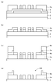
- a method for manufacturing a transfer mask (binary mask) using the mask blank 10 according to the first embodiment will be described with reference to FIG.
- the first pattern to be formed on the light-shielding film 2 is drawn with an electron beam on the resist film 5 having a film thickness of 40 nm or less formed by the spin coating method in the mask blank 10 shown in FIG. 1, and further developed.
- a resist film (resist pattern) 5a having the first pattern is formed (see FIG. 3A).
- This first pattern includes, in addition to the pattern (main pattern) transferred to the semiconductor device, an auxiliary pattern having a line width of about 20 nm.
- an earth pin (not shown) is in contact with the resist film 5 and the second. 2 A ground is secured between the hard mask film 4 and the light-shielding film 2. Therefore, it is possible to suppress charge-up when drawing an electron beam on the resist film 5, and it is possible to perform exposure drawing with high position accuracy.
- the resist pattern 5a as a mask, dry etching using a mixed gas of chlorine-based gas and oxygen-based gas is performed on the second hard mask film 4, and the second hard mask film (hard) having the first pattern is performed.
- the mask pattern) 4a (see FIG. 3B) is formed. After that, the resist pattern 5a is removed.
- the second hard mask pattern 4a as a mask, dry etching using a fluorine-based gas is performed on the first hard mask film 3, and the first hard mask film having the first pattern (first hard mask pattern) is performed. ) 3a (see FIG. 3B).
- another resist film is formed by a spin coating method.
- a laser drawing is performed on the resist film in the range where the first hard mask pattern 3a is formed, and a predetermined process such as a development process is further performed to obtain a resist film (resist) having the second pattern.
- Pattern) 6b (see FIG. 3 (c)) is formed (at this stage, the light-shielding film 2 remains as shown in FIG. 3 (b)).
- the method for manufacturing a semiconductor device of the first embodiment uses a binary mask 100 manufactured by using the binary mask (transfer mask) 100 of the first embodiment or the mask blank 10 of the first embodiment, and a semiconductor. It is characterized in that a transfer pattern is exposed and transferred to a resist film on a substrate. Therefore, when the binary mask 100 of the first embodiment is exposed and transferred to the resist film on the semiconductor device, a pattern can be formed on the resist film on the semiconductor device with an accuracy sufficiently satisfying the design specifications.
- the mask blank according to the second embodiment of the present invention includes a phase shift film between the substrate and the light shielding film, and is used for manufacturing a phase shift mask (transfer mask).
- FIG. 2 shows the configuration of the mask blank of the second embodiment.
- the mask blank 20 according to the second embodiment has a phase shift film 12, a light-shielding film (thin film for pattern formation) 13, a first hard mask film 14, and a second hard mask film 15 on the main surface of the substrate 11.
- a resist film 16 is provided. Since the substrate 11 and the resist film 16 are the same as those in the first embodiment, the description thereof will be omitted.
- the phase shift film 12 is made of a material that can be patterned by dry etching with a fluorine-based gas etching gas, and is specifically made of a material containing silicon.
- the phase shift film 12 has a function of transmitting exposure light with a transmittance of 1% or more (transmittance), and allows the exposure light transmitted through the phase shift film to pass through the air by the same distance as the thickness of the phase shift film. It is preferable to have a function of causing a phase difference of 150 degrees or more and 210 degrees or less with the passing exposure light. Further, the transmittance of the phase shift film 12 is more preferably 2% or more. The transmittance of the phase shift film 12 is preferably 30% or less, more preferably 20% or less.
- the phase shift film 12 is preferably made of a material containing nitrogen (N) in addition to silicon.
- the phase shift film 12 may further contain one or more elements selected from metalloid elements, non-metal elements, and metal elements, as long as patterning is possible by dry etching using a fluorine-based gas.
- the metalloid element may be any metalloid element in addition to silicon.
- the non-metal element may be any non-metal element in addition to nitrogen, and contains one or more elements selected from, for example, oxygen (O), carbon (C), fluorine (F) and hydrogen (H). Is preferable.
- Metal elements include molybdenum (Mo), tungsten (W), titanium (Ti), tantalum (Ta), zirconium (Zr), hafnium (Hf), niobium (Nb), vanadium (V), cobalt (Co), and chromium. Examples thereof include (Cr), nickel (Ni), ruthenium (Ru), tin (Sn), boron (B), and germanium (Ge).
- the film thickness of the phase shift film 12 is preferably 80 nm or less, and more preferably 70 nm or less.
- the film thickness of the phase shift film 12 is preferably 50 nm or more. This is because 50 nm or more is required to make the phase difference of the phase shift film 12 150 degrees or more while forming the phase shift film 12 from an amorphous material.
- the phase shift film 12 can be applied to either a single-layer structure or a laminated structure having two or more layers. Further, each layer of the single-layer structure or the laminated structure may have a structure having substantially the same composition in the thickness direction of the film or the layer, or may have a structure in which the composition is inclined in the thickness direction of the layer.
- the phase shift film 12 is formed in a region smaller than the region in which the light-shielding film 13 is formed in a plan view (on the main surface of the substrate 1).
- the region in which the phase shift film 12 is formed is required to have a size including at least a pattern transfer region.
- the phase shift film 12 is formed so as to cover a region including at least a rectangular region having a side of 132 mm with respect to the center of the main surface of the substrate 11.
- the refractive index n with respect to the exposure light (ArF exposure light) of the phase shift film is preferably 1.9 or more in order to satisfy the above-mentioned optical characteristics and various conditions related to the film thickness. It is more preferable that it is 0.0 or more. Further, the refractive index n of the phase shift film 12 is preferably 3.1 or less, and more preferably 2.7 or less.
- the extinction coefficient k of the phase shift film 12 with respect to the ArF exposure light is preferably 0.26 or more, and more preferably 0.29 or more. The extinction coefficient k of the phase shift film 12 is preferably 0.62 or less, and more preferably 0.54 or less.
- the refractive index n and the extinction coefficient k of the thin film including the phase shift film 12 are not determined only by the composition of the thin film.
- the film density and crystal state of the thin film are also factors that influence the refractive index n and the extinction coefficient k. Therefore, various conditions for forming a thin film by reactive sputtering are adjusted so that the thin film has a desired refractive index n and an extinction coefficient k.
- a mixed gas of a noble gas and a reactive gas oxygen gas, nitrogen gas, etc.
- the mask blank 20 includes a light-shielding film 13 on the phase shift film 12.
- the same light-shielding film 2 as described in the first embodiment is applicable.
- the film thickness of the light-shielding film 13 is preferably 50 nm or less, and more preferably 45 nm or less.
- the film thickness of the light-shielding film 13 is preferably 20 nm or more from the viewpoint of ensuring the optical density and the conductivity.
- the light-shielding film 13 forms a light-shielding band or the like with a laminated structure with the phase-shift film 12. For this reason, the light-shielding film 13 is required to secure an optical density (OD) larger than 2.0 in a laminated structure with the phase shift film 12, and is preferably an OD of 2.8 or more. It is more preferable to have an OD of 0 or more.
- OD optical density
- the first hard mask film 14 is formed on the light-shielding film 13.
- the first hard mask film 14 is formed of a material containing oxygen and one or more elements selected from silicon and tantalum so as to have etching selectivity with respect to the etching gas used when etching the light shielding film 13. ing.
- the specific material and film thickness are the same as those of the first hard mask film 3 in the first embodiment.
- the first hard mask film 14 is formed in a region smaller than the region in which the light-shielding film 13 is formed in a plan view (on the main surface of the substrate 1). With such a configuration, it becomes easy to bring the light-shielding film 13 and the second hard mask film 15 into contact with each other at least in a part.
- the first hard mask film 14 may have a size necessary to cover the pattern transfer region in which the phase shift film 12 is formed.
- the first hard mask film 14 is formed so as to cover a region including at least a rectangular region having a side of 132 mm with respect to the center of the main surface of the substrate 11.
- the second hard mask film 15 is laminated on the first hard mask film 14.
- the second hard mask film 15 needs to have high etching selectivity with respect to the etching gas when patterning the first hard mask film 14.
- the second hard mask film 15 preferably contains a transition metal.
- the specific material and film thickness are the same as those of the second hard mask film 4 in the first embodiment. Further, it is preferable that the region on the main surface of the substrate 11 on which the second hard mask film 15 is formed is larger than the region on which the first hard mask film 14 is formed.
- the region where the first hard mask film 14 is formed is smaller than the region where the light-shielding film 13 is formed, so that the second hard mask film 15 and the light-shielding film 13 are the first hard.
- the second hard mask film 15 and the light-shielding film 13 can be formed so as to be in contact with each other on the outside of the mask film 14, and the conductivity can be ensured in the outer peripheral side region.
- the second hard mask film 15 is formed up to a region beyond the outer peripheral edge of the region where the first hard mask film 14 is formed (that is, the first hard mask film 14 is entirely formed by the second hard mask film 15. Is covered.) Is preferable.
- the second hard mask film 15 is partially formed up to a region beyond the outer peripheral edge of the region where the first hard mask film 14 is formed so as to be in contact with the light-shielding film 13, and the other parts are the first hard. It may be formed in the same region as the region where the mask film 14 is formed.
- the phase shift film 12, the light-shielding film 13, the first hard mask film 14, and the second hard mask film 15 can be formed by forming a film by a reactive sputtering method, respectively, as in the first embodiment. Further, when the phase shift film 12, the light-shielding film 13, the first hard mask film 14, and the second hard mask film 15 are formed, the film formation region of each film is formed by adjusting the opening region of the mask shield. It is possible to adjust to a desired region. Further, the resist film 16 is formed by a spin coating method.
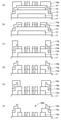
- a method for manufacturing a transfer mask (phase shift mask) using the mask blank 20 according to the second embodiment will be described with reference to FIG.
- a first pattern to be formed on the phase shift film 12 is drawn with an electron beam on the resist film 16 having a film thickness of 40 nm or less formed by the spin coating method in the mask blank 20 shown in FIG. 2, and further developed.
- a resist film (resist pattern) 16a having the first pattern is formed by performing a predetermined process such as (see FIG. 4A).
- This first pattern includes, in addition to the pattern (main pattern) transferred to the semiconductor device, an auxiliary pattern having a line width of about 20 nm.
- an earth pin (not shown) is in contact with the resist film 16 and the first. 2 A ground is secured between the hard mask film 15 and the light-shielding film 13. Therefore, it is possible to suppress charge-up when drawing an electron beam on the resist film 16, and it is possible to perform exposure drawing with high position accuracy (note that also when forming the resist patterns 17b and 18c described later). Similarly, charge-up can be suppressed and exposure drawing with high position accuracy can be performed).
- the resist pattern 16a as a mask, dry etching using a mixed gas of chlorine-based gas and oxygen-based gas is performed on the second hard mask film 15, and the second hard mask film (hard) having the first pattern is performed.
- the mask pattern) 15a (see FIG. 4B) is formed. After that, the resist pattern 16a is removed.
- the second hard mask pattern 15a As a mask, dry etching using a fluorine-based gas is performed on the first hard mask film 14, and the first hard mask film having the first pattern (first hard mask pattern) is performed. ) 14a (see FIG. 4B). Subsequently, another resist film is formed by a spin coating method. After that, a laser drawing is performed on the resist film in the range where the first hard mask pattern 14a is formed, and a predetermined process such as a development process is further performed to obtain a resist film (resist) having the second pattern. Pattern) 17b (see FIG. 4 (c)) is formed (at this stage, the light-shielding film 13 and the second hard mask pattern 15a remain as shown in FIG. 4 (b)).
- phase-shift pattern 12a having the first pattern (FIG. 4 (d). )reference).
- first hard mask pattern 14a is removed (see FIG. 4D).
- resist pattern 17b is removed, a cleaning step is performed, and another resist film is formed by a spin coating method.
- a third pattern to be formed on the light-shielding film 13 is drawn with an electron beam on the resist film, and a predetermined process such as a development process is performed to obtain a resist film (resist pattern) having the third pattern.
- a phase shift mask 200 manufactured by using the phase shift mask 200 according to the second embodiment or the mask blank 20 according to the first embodiment is used on a semiconductor substrate. It is characterized by exposing and transferring a transfer pattern to a resist film. Therefore, when the phase shift mask 200 of the second embodiment is exposed and transferred to the resist film on the semiconductor device, a pattern can be formed on the resist film on the semiconductor device with an accuracy sufficiently satisfying the design specifications.
- the mask blank of the present invention may be a reflective mask blank used when manufacturing a reflective mask for EUV lithography (Extreme Ultraviolet Lithography).
- EUV lithography Extreme Ultraviolet Lithography
- the absorber film is composed of the above-mentioned pattern-forming thin film.
- the multilayer reflective film, the protective film, the absorber film (the thin film for pattern formation), the first hard mask film, and the second hard mask film are laminated in this order on the substrate. It is preferable that the configurations of the absorber membrane, the first hard mask membrane, and the second hard mask membrane are the same as those shown in each of the above embodiments.
- the absorber membrane is preferably formed of the above-mentioned chromium-containing material.
- a material containing ruthenium may be used as the absorber membrane. Examples of the material containing ruthenium in this case include ruthenium metal alone and materials containing at least one of nitrogen and oxygen in ruthenium.
- the multilayer reflective film imparts a function of reflecting EUV light in a reflective mask.
- the multilayer reflective film is a multilayer film in which each layer containing elements having different refractive indexes as main components is periodically laminated.
- a multilayer reflective film a thin film of a light element or a compound thereof (high refractive index layer) which is a high refractive index material and a thin film of a heavy element or a compound thereof which is a low refractive index material (low refractive index layer).
- a multilayer film in which and are alternately laminated for about 40 to 60 cycles (pairs) is used.
- the high refractive index layer for example, a material containing silicon (Si) can be used.
- silicon in addition to elemental silicon, silicon contains at least one element selected from boron (B), carbon (C), zirconium (Zr), nitrogen (N) and oxygen (O). Silicon compounds can be used.
- the low refractive index layer for example, at least one metal simple substance selected from molybdenum (Mo), ruthenium (Ru), rhodium (Rh), and platinum (Pt), or an alloy thereof can be used.
- a Mo / Si periodic laminated film in which layers containing Mo and layers containing Si are alternately laminated for about 40 to 60 cycles is preferably used.
- the protective film may be, for example, a material containing silicon (Si), silicon (Si) and oxygen (O), a material containing silicon (Si) and nitrogen (N), silicon (Si), oxygen (O) and nitrogen (N). ) Can be used as a silicon-based material.
- the absorber film is formed of a material containing ruthenium
- the protective film is composed of chromium (Cr) or chromium (Cr), oxygen (O), nitrogen (N), and carbon (C).
- Cr chromium
- Cr chromium
- Cr chromium
- oxygen (O) nitrogen
- N nitrogen
- C carbon
- Examples of materials containing ruthenium include ruthenium alone, ru with titanium (Ti), niobium (Nb), molybdenum (Mo), zirconium (Zr), ittrium (Y), boron (B), and lanthanum (La). , Ru alloys containing at least one metal selected from cobalt (Co), ruthenium (Re), and rhodium (Rh), and materials containing nitrogen thereof.
- Example 1 Manufacturing of mask blank
- a substrate 11 made of synthetic quartz glass having a main surface dimension of about 152 mm ⁇ about 152 mm and a thickness of about 6.35 mm was prepared.
- the main surface of the substrate 11 is polished to a predetermined surface roughness (Rq of 0.2 nm or less), and then subjected to a predetermined cleaning treatment and a drying treatment.
- a phase shift film 12 made of molybdenum, silicon and nitrogen is formed on the substrate 11 with a thickness of 69 nm by reactive sputtering (DC sputtering) using a mixed gas of Ar), nitrogen (N 2) and helium (He) as the sputtering gas. Formed by gas.
- a masking plate was used during the sputtering to form the phase shift film 12.
- the masking plate used has a 146 mm square opening relative to the center of the substrate (ie, the design area is a 146 mm square area).
- the substrate 11 on which the phase shift film 12 was formed was heat-treated to reduce the film stress of the phase shift film 12 and to form an oxide layer on the surface layer.
- a heating treatment was performed in the atmosphere using a heating furnace (electric furnace) with a heating temperature of 450 ° C. and a heating time of 1 hour.
- the transmittance and phase difference of the heat-treated phase shift film 12 with respect to light having a wavelength of 193 nm were measured using a phase shift amount measuring device (MPM193 manufactured by Lasertec), the transmittance was 6.0% and the phase difference was high. It was 177.0 degrees (deg).
- the substrate 11 on which the phase shift film 12 is formed is installed in the single-wafer DC sputtering apparatus, and argon (Ar), carbon dioxide (CO 2 ) and helium (He) are used using a chromium (Cr) target.
- Reactive sputtering (DC sputtering) was performed in the mixed gas atmosphere of.
- a masking plate was also used during sputtering for forming the light-shielding film 13.
- the masking plate used here has a square opening with a side of 150 mm with respect to the center of the substrate (that is, the design area is a square area with a side of 150 mm).
- the size of one side of the main surface of the substrate 11 is 151.2 mm, and the margin with respect to the design area is considerably small.
- the substrate 11 on which the light-shielding film (CrOC film) 13 was formed was heat-treated. Specifically, a hot plate was used to perform heat treatment in the atmosphere at a heating temperature of 280 ° C. and a heating time of 5 minutes. After the heat treatment, a spectrophotometer (Cary4000 manufactured by Agilent Technologies) was used on the substrate 11 on which the phase shift film 12 and the light shielding film 13 were laminated, and the ArF excimer laser having a laminated structure of the phase shift film 12 and the light shielding film 13 was used. When the optical density at the wavelength of light (about 193 nm) was measured, it was confirmed that it was 3.0 or more.
- a substrate 11 on which a phase shift film 12 and a light-shielding film 13 are laminated is installed in a single-wafer DC sputtering apparatus, and an argon (Ar) gas and oxygen (O 2) are used using a silicon (Si) target.
- the gas was a sputtering gas
- the first hard mask film 14 was formed by DC sputtering.
- a masking plate was used during the sputtering to form the first hard mask film 14.
- the masking plate used has a 146 mm square opening relative to the center of the substrate (ie, the design area is a 146 mm square area).
- the design area is a 146 mm square area.
- the second hard mask film 15 (CrOCN film Cr: 54.7 atomic%, O: 22.2 atomic%, C: 11.9 atomic%, N: 11. 2 atomic%) was formed to a thickness of 3 nm.
- a substrate 11 on which a phase shift film 12, a light shielding film 13 and a first hard mask film 14 are laminated is installed in a single-wafer DC sputtering apparatus, and an argon (Cr) target is used to obtain argon (Cr).
- Reactive sputtering (DC sputtering) was performed in a mixed gas atmosphere of Ar), carbon dioxide (CO 2 ), nitrogen (N 2) and helium (He).
- a masking plate was used during the sputtering to form the second hard mask film 15.
- the masking plate used has a 148 mm square opening relative to the center of the substrate (ie, the design area is a 148 mm square area).
- a second hard mask film was formed on another substrate with a thickness of 3 nm, and the film density was measured and found to be 4.9 g / cm 3 . Moreover, when the sheet resistance value was measured, it was 200 k ⁇ . Then, after performing a predetermined cleaning treatment, a resist film 16 was formed with a film thickness of 40 nm by a spin coating method to produce the mask blank 20 of Example 1.
- SF 4 gas was used as the fluorine-based gas to create a phase shift pattern 12a (see FIG. 4 (b)).
- a multi-beam writer equipped with two electron guns is used, and a second hard mask film 15 and a light-shielding film outside the first hard mask film 14 are used.
- a ground pin (not shown) was in contact with the predetermined region in contact with 13.
- electron beams were drawn at desired positions on each resist film, and the desired resist patterns 16a, 17b, and 18c could be formed.
- the resist pattern 16a included a fine SRAF pattern having a line width of 20 nm in addition to the main pattern for transfer.
- the length of the pattern was measured by a length measuring SEM (CD-SEM: Critical Dimension-Scanning Electron Microscope) centering on the region where the SRAF pattern having a line width of 20 nm was formed. .. As a result, it was confirmed that the phase shift pattern was formed with good LER not only for the main pattern for transfer but also for the fine SRAF pattern having a line width of 20 nm.
- Comparative Example 1 Manufacturing of mask blank
- the mask blank of Comparative Example 1 was manufactured by the same procedure as that of Example 1 except for the hard mask film.
- HMDS Hexamethyldisilazane
- Comparative Example 2 Manufacturing of mask blank
- the mask blank of Comparative Example 2 was manufactured by the same procedure as in Example 1 except for the hard mask film.
- the hard mask film of Comparative Example 2 only the configuration of the second hard mask film 15 is changed from that of Example 1.
- a resist film having a diameter of 40 nm was formed on the hard mask film by a spin coating method.
- phase shift mask a halftone type phase shift mask was manufactured using the mask blank of Comparative Example 2.
- the process of manufacturing the phase shift mask is the same as that described in the first embodiment.
- the earth pin is brought into contact with the predetermined region where the second hard mask film of Comparative Example 2 and the light-shielding film are in contact with each other. I left it.
- the phase shift mask of Comparative Example 2 was manufactured in the same manner as in Example 1.
- the length of the pattern was measured by a length measuring SEM (CD-SEM: Critical Dimension-Scanning Electron Microscope) centering on the region where the SRAF pattern having a line width of 20 nm was formed.
- SEM Critical Dimension-Scanning Electron Microscope
- Substrate 2 Light-shielding film (thin film for pattern formation) 2b Light-shielding film with a second pattern (light-shielding pattern) 3 First hard mask film 3a First hard mask film having a first pattern (first hard mask pattern) 4 Second hard mask film 4a A second hard mask film having a first pattern (second hard mask pattern) 4b Second hard mask film having a second pattern (second hard mask pattern) 5 Resist film 5a A resist film having a first pattern (resist pattern) 6b Resist film having a second pattern (resist pattern) 10 Mask blank (binary mask blank) 11 Substrate 12 Phase shift film (thin film for pattern formation) 12a Phase shift film having a first pattern (phase shift pattern) 13 Light-shielding film (thin film for pattern formation) 13a Light-shielding film having the first pattern (light-shielding pattern) 13c Light-shielding film with a third pattern (light-shielding pattern) 14 1st hard mask film 14a 1s
Landscapes
- Physics & Mathematics (AREA)
- General Physics & Mathematics (AREA)
- Chemical & Material Sciences (AREA)
- Chemical Kinetics & Catalysis (AREA)
- Engineering & Computer Science (AREA)
- Materials Engineering (AREA)
- Mechanical Engineering (AREA)
- Metallurgy (AREA)
- Organic Chemistry (AREA)
- Preparing Plates And Mask In Photomechanical Process (AREA)
- Physical Vapour Deposition (AREA)
Abstract
Description
また、バイナリマスクにおいても、遮光膜上にエッチングマスク膜(ハードマスク膜)が積層された構造を有するマスクブランクが以前より知られている。
また、特許文献2には、電子線描画によりレジストパターンを形成する電子線描画用のマスクブランクであって、透明基板上に、遮光膜と、この遮光膜のエッチングに対して耐性を有する無機系材料からなるエッチングマスク膜がこの順に形成されたマスクブランクの製造方法であって、エッチングマスク膜を成膜する際に、基板の少なくとも側面には成膜されないように遮蔽板にて遮蔽する製造方法が開示されている。
そこで解像度を上げるために、プロセス定数k1(k1=解像線幅×投影光学系の開口数/露光光の波長)の値を小さくすることによって微細化を図る超解像技術が近年提案されている。このような超解像技術の一つとして、露光光学系の特性に応じてマスクパターンに補助パターンや線幅オフセットを与えてマスクパターンを最適化する方法がある。
補助パターンを用いる方法は、ウェハ上に転写されるパターン(以後、主パターンと称する。)の近傍に、投影光学系の解像限界以下であってウェハ上には転写されないパターン(以後、補助パターンと称する。)を配置し、主パターンの解像度と焦点深度を向上させる効果を有する転写用マスクを用いるリソグラフィ方法である。補助パターンはSRAF(Sub Resolution Assist Feature)とも呼ばれている(以後、本発明では補助パターンをSRAFとも称する。)。
しかし、従来のマスクブランクでは、20nm程度といった微小な寸法の補助パターンを有する転写用マスクを製作することが困難であることが判明した。
(構成1)
基板の主表面上に、パターン形成用薄膜、第1ハードマスク膜、第2ハードマスク膜がこの順に積層した構造を備えるマスクブランクであって、
前記パターン形成用薄膜は、遷移金属を含有し、
前記第1ハードマスク膜は、ケイ素およびタンタルから選ばれる1以上の元素と酸素とを含有し、
前記第2ハードマスク膜は、遷移金属を含有し、
前記第2ハードマスク膜の遷移金属の含有量は、前記パターン形成用薄膜の遷移金属の含有量よりも少なく、
前記主表面上における第1ハードマスク膜が形成されている領域は、前記パターン形成用薄膜が形成されている領域よりも小さく、
前記第2ハードマスク膜と前記パターン形成用薄膜は、少なくとも一部で接している
ことを特徴とするマスクブランク。
前記第2ハードマスク膜の酸素および窒素の合計含有量は、前記パターン形成用薄膜の酸素および窒素の合計含有量よりも多いことを特徴とする構成1記載のマスクブランク。
(構成3)
前記主表面上における第2ハードマスク膜が形成されている領域は、前記第1ハードマスク膜が形成されている領域よりも大きいことを特徴とする構成1または2に記載のマスクブランク。
前記パターン形成用薄膜の遷移金属の含有量と前記第2ハードマスク膜の遷移金属の含有量との間の差は、10原子%以上であることを特徴とする構成1から3のいずれかに記載のマスクブランク。
(構成5)
前記第2ハードマスク膜の酸素および窒素の合計含有量は、30原子%以上であることを特徴とする構成1から4のいずれかに記載のマスクブランク。
前記第2ハードマスク膜の膜厚は、5nm以下であることを特徴とする構成1から5のいずれかに記載のマスクブランク。
(構成7)
前記第1ハードマスク膜の酸素および窒素の合計含有量は、50原子%以上であることを特徴とする構成1から6のいずれかに記載のマスクブランク。
前記第1ハードマスク膜の酸素含有量は、50原子%以上であることを特徴とする構成1から7のいずれかに記載のマスクブランク。
(構成9)
前記第1ハードマスク膜の膜厚は、7nm以上であることを特徴とする構成1から8のいずれかに記載のマスクブランク。
前記パターン形成用薄膜の膜厚は、60nm以下であることを特徴とする構成1から9のいずれかに記載のマスクブランク。
前記パターン形成用薄膜は、遮光膜であり、前記基板と前記遮光膜の間に位相シフト膜を備えることを特徴とする構成1から10のいずれかに記載のマスクブランク。
前記位相シフト膜は、ケイ素を含有することを特徴とする構成11記載のマスクブランク。
前記位相シフト膜は、露光光を1%以上の透過率で透過させる機能と、前記位相シフト膜を透過した前記露光光に対して前記位相シフト膜の厚さと同じ距離だけ空気中を通過した前記露光光との間で150度以上210度以下の位相差を生じさせる機能とを有することを特徴とする構成11または12に記載のマスクブランク。
構成1から10のいずれかに記載のマスクブランクを用いる転写用マスクの製造方法であって、
前記第2ハードマスク膜上に形成された転写パターンを有するレジスト膜をマスクとし、酸素含有塩素系ガスを用いたドライエッチングにより、前記第2ハードマスク膜に転写パターンを形成する工程と、
前記転写パターンが形成された第2ハードマスク膜をマスクとし、フッ素系ガスを用いたドライエッチングにより、前記第1ハードマスク膜に転写パターンを形成する工程と、
前記転写パターンが形成された第1ハードマスク膜をマスクとし、酸素含有塩素系ガスを用いたドライエッチングにより、前記パターン形成用薄膜に転写パターンを形成する工程とを有することを特徴とする転写用マスクの製造方法。
構成11から13のいずれかに記載のマスクブランクを用いる転写用マスクの製造方法であって、
前記第2ハードマスク膜上に形成された転写パターンを有するレジスト膜をマスクとし、酸素含有塩素系ガスを用いたドライエッチングにより、前記第2ハードマスク膜に転写パターンを形成する工程と、
前記転写パターンが形成された第2ハードマスク膜をマスクとし、フッ素系ガスを用いたドライエッチングにより、前記第1ハードマスク膜に転写パターンを形成する工程と、
前記転写パターンが形成された第1ハードマスク膜をマスクとし、酸素含有塩素系ガスを用いたドライエッチングにより、前記遮光膜に転写パターンを形成する工程と、
前記転写パターンが形成された遮光膜をマスクとし、フッ素系ガスを用いたドライエッチングにより、前記位相シフト膜に転写パターンを形成する工程と
を有することを特徴とする転写用マスクの製造方法。
構成14または15に記載の転写用マスクの製造方法で製造された転写用マスクを用い、半導体基板上のレジスト膜に転写パターンを露光転写する工程を有することを特徴とする半導体デバイスの製造方法。
上述のような線幅20nm程度の補助パターンを遷移金属系材料からなるパターン形成用薄膜(遮光膜等)に形成する場合、有機系材料のレジストパターンをマスクとするドライエッチングでパターン形成用薄膜に補助パターンを形成することは困難である。ドライエッチング時、レジストパターンの膜厚方向へのエッチング量が比較的多く、レジスト膜を厚くする必要があるためである。また、レジストパターンの側壁方向のへのエッチング量(サイドエッチング量)も比較的大きい。一般に、このサイドエッチングの影響を見込んで線幅を実際に形成する線幅よりも大きくして、レジスト膜にパターンを電子線で描画露光する。サイドエッチング量が大きいと、この調整が困難になる。
すなわち、本発明のマスクブランクは、基板の主表面上に、パターン形成用薄膜、第1ハードマスク膜、第2ハードマスク膜がこの順に積層した構造を備えるマスクブランクであって、パターン形成用薄膜は、遷移金属を含有し、第1ハードマスク膜は、ケイ素およびタンタルから選ばれる1以上の元素と酸素とを含有し、第2ハードマスク膜は、遷移金属を含有し、第2ハードマスク膜の遷移金属の含有量は、パターン形成用薄膜の遷移金属の含有量よりも少なく、主表面上における第1ハードマスク膜が形成されている領域は、パターン形成用薄膜が形成されている領域よりも小さく、第2ハードマスク膜とパターン形成用薄膜は、少なくとも一部で接していることを特徴とするものである。
[マスクブランクとその製造]
以下、実施の形態について図面を参照しながら説明を行う。
図1は、本発明の第1の実施形態に係るマスクブランク(バイナリマスクブランク)10の構成を示す断面図である。図1に示す本発明のマスクブランク10は、基板1上に、遮光膜(パターン形成用薄膜)2、第1ハードマスク膜3、第2ハードマスク膜4、レジスト膜5がこの順に積層された構造を有する。
ケイ素と酸素を含有する材料としては、SiO2、SiONなどを適用することが好ましい。この場合、第1ハードマスク膜3は、ケイ素および酸素の合計含有量が96原子%以上であることが好ましく、98原子%以上であるとより好ましい。また、第1ハードマスク膜3は、ケイ素、窒素および酸素の合計含有量が96原子%以上であることが好ましく、98原子%以上であるとより好ましい。なお、ケイ素と酸素を含有する材料で形成される第1ハードマスク膜3は、遮光膜2および第2ハードマスク膜4との間で、十分なエッチング選択性が得られる範囲で遷移金属を含有してもよい。
また、タンタルと酸素を含有する材料としては、タンタルと酸素のほか、窒素、ホウ素および炭素から選ばれる一以上の元素を含有させた材料などが挙げられる。たとえば、TaO、TaON、TaBO、TaBON、TaCO、TaCON、TaBOCNなどが挙げられる。この場合、第1ハードマスク膜3は、これらの材料のうち、ホウ素を含有するものであることが好ましい。
また、第2ハードマスク膜4のエッチングレートを一定以上の大きさにするために、第2ハードマスク膜4の酸素および窒素の合計含有量は、30原子%以上であると好ましく、32原子%以上であることが好ましい。また、第2ハードマスク膜4の酸素含有量は、20原子%以上であることが好ましい。
また、第2ハードマスク膜4の膜密度は、3.5g/cm3~7.0g/cm3であると好ましい。
また、成膜装置内の回転ステージに基板1を配置し、遮光膜2、第1ハードマスク膜3、第2ハードマスク膜4を成膜する際に、基板1の主表面上にマスクシールドを設置し、そのマスクシールドの開口領域を調整することで、それぞれの膜の基板1の主表面上の成膜領域を所望の領域に調整することが可能となる。
また、レジスト膜5は、スピン塗布法によって形成される。
この第1の実施形態に係るマスクブランク10を用いた転写用マスク(バイナリマスク)の製造方法について、図3を用いて説明する。
図1に示されるマスクブランク10においてスピン塗布法によって形成された膜厚40nm以下のレジスト膜5に対して、遮光膜2に形成すべき第1のパターンを電子線で描画し、さらに現像処理等の所定の処理を行うことによって、第1のパターンを有するレジスト膜(レジストパターン)5aを形成する(図3(a)参照)。この第1のパターンには、半導体デバイスに転写されるパターン(主パターン)の他に、線幅20nm程度の補助パターンも含まれている。
続いて、レジストパターン5aをマスクとして、塩素系ガスと酸素系ガスの混合ガスを用いたドライエッチングを第2ハードマスク膜4に対して行い、第1のパターンを有する第2ハードマスク膜(ハードマスクパターン)4a(図3(b)参照)を形成する。その後、レジストパターン5aを除去する。
第1の実施形態の半導体デバイスの製造方法は、第1の実施形態のバイナリマスク(転写用マスク)100または第1の実施形態のマスクブランク10を用いて製造されたバイナリマスク100を用い、半導体基板上のレジスト膜に転写用パターンを露光転写することを特徴としている。このため、第1の実施形態のバイナリマスク100を用いて半導体デバイス上のレジスト膜に露光転写すると、半導体デバイス上のレジスト膜に設計仕様を十分に満たす精度でパターンを形成することができる。
[マスクブランクとその製造]
本発明の第2の実施形態に係るマスクブランクは、基板と遮光膜との間に位相シフト膜を備えるものであり、位相シフトマスク(転写用マスク)を製造するために用いられるものである。図2に、この第2の実施形態のマスクブランクの構成を示す。この第2の実施形態に係るマスクブランク20は、基板11の主表面上に、位相シフト膜12、遮光膜(パターン形成用薄膜)13、第1ハードマスク膜14、第2ハードマスク膜15、レジスト膜16を備えている。基板11、レジスト膜16は第1の実施形態と同様であるので、説明を省略する。
この場合の遮光膜13においても、上記の第1の実施形態で説明した遮光膜2と同様のものが適用可能である。ただし、後述の通り、位相シフト膜12の上に設ける遮光膜13の場合、バイナリマスク用の遮光膜2ほどのODは求められない。このため、遮光膜13の膜厚は、50nm以下であることが好ましく、45nm以下であることがより好ましい。一方、遮光膜13の膜厚は、光学濃度の確保と導電性の確保の観点から、20nm以上であることが好ましい。
また、基板11の主表面上における第2ハードマスク膜15が形成されている領域は、第1ハードマスク膜14が形成されている領域よりも大きいことが好ましい。これにより、上述の通り、第1ハードマスク膜14が形成されている領域は、遮光膜13が形成されている領域よりも小さいので、第2ハードマスク膜15と遮光膜13とが第1ハードマスク膜14の外側において接するように、第2ハードマスク膜15と遮光膜13を成膜することができ、この外周側領域において導電性を確保することが可能となる。
また、位相シフト膜12、遮光膜13、第1ハードマスク膜14、第2ハードマスク膜15を成膜する際に、マスクシールドの開口領域を調整することで、それぞれの膜の成膜領域を所望の領域に調整することが可能となる。
また、レジスト膜16は、スピン塗布法によって形成される。
この第2の実施形態に係るマスクブランク20を用いた転写用マスク(位相シフトマスク)の製造方法について、図4を用いて説明する。
図2に示されるマスクブランク20においてスピン塗布法によって形成された膜厚40nm以下のレジスト膜16に対して、位相シフト膜12に形成すべき第1のパターンを電子線で描画し、さらに現像処理等の所定の処理を行うことによって第1のパターンを有するレジスト膜(レジストパターン)16aを形成する(図4(a)参照)。この第1のパターンには、半導体デバイスに転写されるパターン(主パターン)の他に、線幅20nm程度の補助パターンも含まれている。
このとき、第1ハードマスク膜14よりも外側における、第2ハードマスク膜15と遮光膜13とが接触している所定の領域において、図示しないアースピンが接触しており、レジスト膜16と、第2ハードマスク膜15と、遮光膜13との間でアースが確保されている。このため、レジスト膜16に電子線を描画する際におけるチャージアップを抑制することができ、位置精度の高い露光描画を行うことができる(なお、後述するレジストパターン17b、18cを形成するときにも、同様にチャージアップを抑制することができ、位置精度の高い露光描画を行うことができる)。
続いて、レジストパターン16aをマスクとして、塩素系ガスと酸素系ガスの混合ガスを用いたドライエッチングを第2ハードマスク膜15に対して行い、第1のパターンを有する第2ハードマスク膜(ハードマスクパターン)15a(図4(b)参照)を形成する。その後、レジストパターン16aを除去する。
そして、レジストパターン17bを除去し、洗浄工程を行って、別のレジスト膜をスピン塗布法によって形成する。その後、このレジスト膜に対して、遮光膜13に形成すべき第3のパターンを電子線で描画し、さらに現像処理等の所定の処理を行うことによって第3のパターンを有するレジスト膜(レジストパターン)18c(図4(e)参照)を形成する。その後、レジストパターン18cをマスクとして、塩素系ガスと酸素ガスの混合ガスを用いたドライエッチングを遮光膜13に対して行い、第3のパターンを有する遮光膜(遮光パターン)13cを形成する。そして、レジストパターン18cを除去し、洗浄工程を行って、転写用マスク(位相シフトマスク)200を製造することができる(図4(f)参照)。
第2の実施形態の半導体デバイスの製造方法は、第2の実施形態の位相シフトマスク200または第1の実施形態のマスクブランク20を用いて製造された位相シフトマスク200を用い、半導体基板上のレジスト膜に転写用パターンを露光転写することを特徴としている。このため、第2の実施形態の位相シフトマスク200を用いて半導体デバイス上のレジスト膜に露光転写すると、半導体デバイス上のレジスト膜に設計仕様を十分に満たす精度でパターンを形成することができる。
(実施例1)
[マスクブランクの製造]
図2を参照し、主表面の寸法が約152mm×約152mmで、厚さが約6.35mmの合成石英ガラスからなる基板11を準備した。この基板11は、主表面が所定の表面粗さ(Rqで0.2nm以下)に研磨され、その後、所定の洗浄処理及び乾燥処理が施されている。
別の基板上に第1ハードマスク膜14を12nmの厚さで成膜して、膜密度を測定したところ、1.8g/cm3であった。また、シート抵抗値を測定したところ、40kΩであった。
別の基板上に第2ハードマスク膜を3nmの厚さで成膜して、膜密度を測定したところ、4.9g/cm3であった。また、シート抵抗値を測定したところ、200kΩであった。
そして、所定の洗浄処理を施した後、レジスト膜16を40nmの膜厚でスピン塗布法により形成し、実施例1のマスクブランク20を製造した。
次に、この実施例1のマスクブランク20を用い、図4を用いて上述した手順で実施例1のハーフトーン型の位相シフトマスク200を製造した。
より具体的には、第2ハードマスク膜15のエッチングには、塩素ガス(Cl2)と酸素ガス(O2)の混合ガス(ガス流量比 Cl2:O2=15:1)を用いて、第2ハードマスクパターン15aを作成した(図4(b)参照)。
また、第1ハードマスク膜14のエッチングには、フッ素系ガスとしてCF4ガスを用いて、第1ハードマスクパターン14aを作成した(図4(b)参照)。
また、遮光膜13のエッチングには、塩素ガス(Cl2)と酸素ガス(O2)の混合ガス(ガス流量比 Cl2:O2=15:1)を用いて、遮光パターン13a、13cを作成した(図4(c)、図4(d)参照)。
また、位相シフト膜12のエッチングには、フッ素系ガスとしてSF4ガスを用いて、位相シフトパターン12aを作成した(図4(b)参照)。
また、これらの一連の工程において、電子線描画の際には、2本の電子銃を備えるマルチビームライターを用い、第1ハードマスク膜14よりも外側における、第2ハードマスク膜15と遮光膜13とが接触している所定の領域において、図示しないアースピンを接触させていた。これにより、それぞれのレジスト膜には所望の位置に電子線が描画され、所望のレジストパターン16a、17b、18cを形成することができた。このレジストパターン16aは、転写用の主パターンに加え、線幅20nmの微細なSRAFパターンを含むものであった。
[マスクブランクの製造]
この比較例1のマスクブランクは、ハードマスク膜以外については、実施例1と同様の手順で製造した。この比較例1のハードマスク膜は、実施例1の第2ハードマスク膜15を形成せずに、第1ハードマスク膜14と同じ材料(SiO2膜 Si:O=34原子%、66原子%)のものを12nmの膜厚で形成した。そして、このハードマスク膜の表面に対してHMDS(Hexamethyldisilazane)処理を行った後、40nmのレジスト膜をスピン塗布法により形成した。
次に、この比較例1のマスクブランクを用い、ハーフトーン型の位相シフトマスクの製造を試みた。
比較例1のマスクブランクに形成したレジスト膜に対し、実施例1と同様の手順で電子線での描画を行った。このとき、比較例1のハードマスク膜と遮光膜が接触している所定の領域においてアースピンを接触させておいた。しかしながら、レジストパターンを形成する過程において、チャージアップが発生してしまい、所望のパターンを描画することができなかった。
[マスクブランクの製造]
この比較例2のマスクブランクは、ハードマスク膜以外については、実施例1と同様の手順で製造した。この比較例2のハードマスク膜は、第2ハードマスク膜15の構成のみを実施例1のものから変更している。具体的には、遮光膜と同じ成膜条件で第2のハードマスク膜をクロム、酸素及び炭素からなる材料(CrOC膜 Cr:O:C=70.4原子%:15.4原子%:14.2原子%)のものを3nmの膜厚で形成した。そして、このハードマスク膜の上に40nmのレジスト膜をスピン塗布法により形成した。
次に、この比較例2のマスクブランクを用い、ハーフトーン型の位相シフトマスクの製造を行った。位相シフトマスクの製造のプロセスは、実施例1において説明したものと同様である。
比較例2のマスクブランクに形成したレジスト膜に対し、電子線での描画を行う際には、比較例2の第2ハードマスク膜と遮光膜が接触している所定の領域においてアースピンを接触させておいた。
このように、実施例1と同様にして、比較例2の位相シフトマスクを製造した。
比較例2の位相シフトマスクに対して、線幅20nmのSRAFパターンが形成されている領域を中心に測長SEM(CD-SEM:Critical Dimension-Scanning Electron Microscope)でパターンの測長を行った。その結果、転写用の主パターンおよび線幅20nmの微細なSRAFパターンともに、パターン自体が形成できていない箇所がいくつも見つかった。これは、40nmの膜厚のレジストパターンをマスクとするドライエッチングで第2ハードマスク膜をパターニングしたときに、第2ハードマスク膜のエッチングレートが遅く、第2ハードマスク膜にパターンが形成し終える前にレジストパターンが消失してしまったことに起因するものと推測される。
2 遮光膜(パターン形成用薄膜)
2b 第2のパターンを有する遮光膜(遮光パターン)
3 第1ハードマスク膜
3a 第1のパターンを有する第1ハードマスク膜(第1ハードマスクパターン)
4 第2ハードマスク膜
4a 第1のパターンを有する第2ハードマスク膜(第2ハードマスクパターン)
4b 第2のパターンを有する第2ハードマスク膜(第2ハードマスクパターン)
5 レジスト膜
5a 第1のパターンを有するレジスト膜(レジストパターン)
6b 第2のパターンを有するレジスト膜(レジストパターン)
10 マスクブランク(バイナリマスクブランク)
11 基板
12 位相シフト膜(パターン形成用薄膜)
12a 第1のパターンを有する位相シフト膜(位相シフトパターン)
13 遮光膜(パターン形成用薄膜)
13a 第1のパターンを有する遮光膜(遮光パターン)
13c 第3のパターンを有する遮光膜(遮光パターン)
14 第1ハードマスク膜
14a 第1のパターンを有する第1ハードマスク膜(第1ハードマスクパターン)
15 第2ハードマスク膜
15a 第1のパターンを有する第2ハードマスク膜(第2ハードマスクパターン)
15b 第2のパターンを有する第2ハードマスク膜(第2ハードマスクパターン)
16 レジスト膜
16a 第1のパターンを有するレジスト膜(レジストパターン)
17b 第2のパターンを有するレジスト膜(レジストパターン)
18c 第3のパターンを有するレジスト膜(レジストパターン)
20 マスクブランク(位相シフトマスクブランク)
100 転写用マスク(バイナリマスク)
200 転写用マスク(位相シフトマスク)
Claims (16)
- 基板の主表面上に、パターン形成用薄膜、第1ハードマスク膜、第2ハードマスク膜がこの順に積層した構造を備えるマスクブランクであって、
前記パターン形成用薄膜は、遷移金属を含有し、
前記第1ハードマスク膜は、ケイ素およびタンタルから選ばれる1以上の元素と酸素とを含有し、
前記第2ハードマスク膜は、遷移金属を含有し、
前記第2ハードマスク膜の遷移金属の含有量は、前記パターン形成用薄膜の遷移金属の含有量よりも少なく、
前記主表面上における第1ハードマスク膜が形成されている領域は、前記パターン形成用薄膜が形成されている領域よりも小さく、
前記第2ハードマスク膜と前記パターン形成用薄膜は、少なくとも一部で接している
ことを特徴とするマスクブランク。 - 前記第2ハードマスク膜の酸素および窒素の合計含有量は、前記パターン形成用薄膜の酸素および窒素の合計含有量よりも多いことを特徴とする請求項1記載のマスクブランク。
- 前記主表面上における第2ハードマスク膜が形成されている領域は、前記第1ハードマスク膜が形成されている領域よりも大きいことを特徴とする請求項1または2に記載のマスクブランク。
- 前記パターン形成用薄膜の遷移金属の含有量と前記第2ハードマスク膜の遷移金属の含有量との間の差は、10原子%以上であることを特徴とする請求項1から3のいずれかに記載のマスクブランク。
- 前記第2ハードマスク膜の酸素および窒素の合計含有量は、30原子%以上であることを特徴とする請求項1から4のいずれかに記載のマスクブランク。
- 前記第2ハードマスク膜の膜厚は、5nm以下であることを特徴とする請求項1から5のいずれかに記載のマスクブランク。
- 前記第1ハードマスク膜の酸素および窒素の合計含有量は、50原子%以上であることを特徴とする請求項1から6のいずれかに記載のマスクブランク。
- 前記第1ハードマスク膜の酸素含有量は、50原子%以上であることを特徴とする請求項1から7のいずれかに記載のマスクブランク。
- 前記第1ハードマスク膜の膜厚は、7nm以上であることを特徴とする請求項1から8のいずれかに記載のマスクブランク。
- 前記パターン形成用薄膜の膜厚は、60nm以下であることを特徴とする請求項1から9のいずれかに記載のマスクブランク。
- 前記パターン形成用薄膜は、遮光膜であり、前記基板と前記遮光膜の間に位相シフト膜を備えることを特徴とする請求項1から10のいずれかに記載のマスクブランク。
- 前記位相シフト膜は、ケイ素を含有することを特徴とする請求項11記載のマスクブランク。
- 前記位相シフト膜は、露光光を1%以上の透過率で透過させる機能と、前記位相シフト膜を透過した前記露光光に対して前記位相シフト膜の厚さと同じ距離だけ空気中を通過した前記露光光との間で150度以上210度以下の位相差を生じさせる機能とを有することを特徴とする請求項11または12に記載のマスクブランク。
- 請求項1から10のいずれかに記載のマスクブランクを用いる転写用マスクの製造方法であって、
前記第2ハードマスク膜上に形成された転写パターンを有するレジスト膜をマスクとし、酸素含有塩素系ガスを用いたドライエッチングにより、前記第2ハードマスク膜に転写パターンを形成する工程と、
前記転写パターンが形成された第2ハードマスク膜をマスクとし、フッ素系ガスを用いたドライエッチングにより、前記第1ハードマスク膜に転写パターンを形成する工程と、
前記転写パターンが形成された第1ハードマスク膜をマスクとし、酸素含有塩素系ガスを用いたドライエッチングにより、前記パターン形成用薄膜に転写パターンを形成する工程とを有することを特徴とする転写用マスクの製造方法。 - 請求項11から13のいずれかに記載のマスクブランクを用いる転写用マスクの製造方法であって、
前記第2ハードマスク膜上に形成された転写パターンを有するレジスト膜をマスクとし、酸素含有塩素系ガスを用いたドライエッチングにより、前記第2ハードマスク膜に転写パターンを形成する工程と、
前記転写パターンが形成された第2ハードマスク膜をマスクとし、フッ素系ガスを用いたドライエッチングにより、前記第1ハードマスク膜に転写パターンを形成する工程と、
前記転写パターンが形成された第1ハードマスク膜をマスクとし、酸素含有塩素系ガスを用いたドライエッチングにより、前記遮光膜に転写パターンを形成する工程と、
前記転写パターンが形成された遮光膜をマスクとし、フッ素系ガスを用いたドライエッチングにより、前記位相シフト膜に転写パターンを形成する工程と
を有することを特徴とする転写用マスクの製造方法。 - 請求項14または15に記載の転写用マスクの製造方法で製造された転写用マスクを用い、半導体基板上のレジスト膜に転写パターンを露光転写する工程を有することを特徴とする半導体デバイスの製造方法。
Priority Applications (3)
| Application Number | Priority Date | Filing Date | Title |
|---|---|---|---|
| US18/010,744 US12468217B2 (en) | 2020-07-15 | 2021-06-17 | Mask blank, method of manufacturing transfer mask, and method of manufacturing semiconductor device |
| CN202180049300.7A CN115917428B (zh) | 2020-07-15 | 2021-06-17 | 掩模坯料、转印用掩模的制造方法及半导体器件的制造方法 |
| KR1020237000626A KR102844825B1 (ko) | 2020-07-15 | 2021-06-17 | 마스크 블랭크, 전사용 마스크의 제조 방법 및 반도체 디바이스의 제조 방법 |
Applications Claiming Priority (2)
| Application Number | Priority Date | Filing Date | Title |
|---|---|---|---|
| JP2020121204A JP7370943B2 (ja) | 2020-07-15 | 2020-07-15 | マスクブランク、転写用マスクの製造方法及び半導体デバイスの製造方法 |
| JP2020-121204 | 2020-07-15 |
Publications (1)
| Publication Number | Publication Date |
|---|---|
| WO2022014248A1 true WO2022014248A1 (ja) | 2022-01-20 |
Family
ID=79555490
Family Applications (1)
| Application Number | Title | Priority Date | Filing Date |
|---|---|---|---|
| PCT/JP2021/023031 Ceased WO2022014248A1 (ja) | 2020-07-15 | 2021-06-17 | マスクブランク、転写用マスクの製造方法及び半導体デバイスの製造方法 |
Country Status (6)
| Country | Link |
|---|---|
| US (1) | US12468217B2 (ja) |
| JP (1) | JP7370943B2 (ja) |
| KR (1) | KR102844825B1 (ja) |
| CN (1) | CN115917428B (ja) |
| TW (1) | TW202217434A (ja) |
| WO (1) | WO2022014248A1 (ja) |
Cited By (1)
| Publication number | Priority date | Publication date | Assignee | Title |
|---|---|---|---|---|
| US20230097280A1 (en) * | 2020-03-19 | 2023-03-30 | Hoya Corporation | Mask blank, transfer mask, and method for manufacturing semiconductor device |
Families Citing this family (2)
| Publication number | Priority date | Publication date | Assignee | Title |
|---|---|---|---|---|
| KR102587396B1 (ko) * | 2022-08-18 | 2023-10-10 | 에스케이엔펄스 주식회사 | 블랭크 마스크 및 이를 이용한 포토마스크 |
| TWI861711B (zh) * | 2023-02-07 | 2024-11-11 | 日商凸版光掩模有限公司 | 空白光罩、光罩及光罩之製造方法 |
Citations (5)
| Publication number | Priority date | Publication date | Assignee | Title |
|---|---|---|---|---|
| JP2006303500A (ja) * | 2005-04-19 | 2006-11-02 | Samsung Electronics Co Ltd | 微細ピッチのハードマスクを用いた半導体素子の微細パターン形成方法 |
| JP2009069677A (ja) * | 2007-09-14 | 2009-04-02 | Hoya Corp | マスクブランク及びマスクの製造方法 |
| JP2018151451A (ja) * | 2017-03-10 | 2018-09-27 | 信越化学工業株式会社 | フォトマスクブランク |
| JP2018151453A (ja) * | 2017-03-10 | 2018-09-27 | 信越化学工業株式会社 | ハーフトーン位相シフト型フォトマスクブランク |
| JP2019503082A (ja) * | 2016-01-20 | 2019-01-31 | アプライド マテリアルズ インコーポレイテッドApplied Materials,Incorporated | 横方向ハードマスク凹部縮小のためのハイブリッドカーボンハードマスク |
Family Cites Families (8)
| Publication number | Priority date | Publication date | Assignee | Title |
|---|---|---|---|---|
| JP5393972B2 (ja) | 2007-11-05 | 2014-01-22 | Hoya株式会社 | マスクブランク及び転写用マスクの製造方法 |
| US9829786B2 (en) * | 2015-06-29 | 2017-11-28 | Taiwan Semiconductor Manufacturing Co., Ltd. | PSM blank for enhancing small size CD resolution |
| JP6573806B2 (ja) * | 2015-08-31 | 2019-09-11 | Hoya株式会社 | マスクブランク、位相シフトマスク、位相シフトマスクの製造方法および半導体デバイスの製造方法 |
| US9921467B2 (en) * | 2015-11-30 | 2018-03-20 | Taiwan Semiconductor Manufacturing Company Ltd. | Mask blank and mask and fabrication method thereof |
| JP2017227824A (ja) * | 2016-06-24 | 2017-12-28 | Hoya株式会社 | マスクブランク、転写用マスクの製造方法および半導体デバイスの製造方法 |
| SG10201911903XA (en) * | 2017-02-27 | 2020-02-27 | Hoya Corp | Mask blank, method for manufacturing transfer mask, and method for manufacturing semiconductor device |
| JP6400763B2 (ja) * | 2017-03-16 | 2018-10-03 | Hoya株式会社 | マスクブランク、転写用マスクおよび半導体デバイスの製造方法 |
| US11453590B2 (en) * | 2018-10-21 | 2022-09-27 | Board Of Regents, The University Of Texas System | Methods to pattern carbon nanotube sheets |
-
2020
- 2020-07-15 JP JP2020121204A patent/JP7370943B2/ja active Active
-
2021
- 2021-06-17 WO PCT/JP2021/023031 patent/WO2022014248A1/ja not_active Ceased
- 2021-06-17 US US18/010,744 patent/US12468217B2/en active Active
- 2021-06-17 CN CN202180049300.7A patent/CN115917428B/zh active Active
- 2021-06-17 KR KR1020237000626A patent/KR102844825B1/ko active Active
- 2021-07-06 TW TW110124785A patent/TW202217434A/zh unknown
Patent Citations (5)
| Publication number | Priority date | Publication date | Assignee | Title |
|---|---|---|---|---|
| JP2006303500A (ja) * | 2005-04-19 | 2006-11-02 | Samsung Electronics Co Ltd | 微細ピッチのハードマスクを用いた半導体素子の微細パターン形成方法 |
| JP2009069677A (ja) * | 2007-09-14 | 2009-04-02 | Hoya Corp | マスクブランク及びマスクの製造方法 |
| JP2019503082A (ja) * | 2016-01-20 | 2019-01-31 | アプライド マテリアルズ インコーポレイテッドApplied Materials,Incorporated | 横方向ハードマスク凹部縮小のためのハイブリッドカーボンハードマスク |
| JP2018151451A (ja) * | 2017-03-10 | 2018-09-27 | 信越化学工業株式会社 | フォトマスクブランク |
| JP2018151453A (ja) * | 2017-03-10 | 2018-09-27 | 信越化学工業株式会社 | ハーフトーン位相シフト型フォトマスクブランク |
Cited By (1)
| Publication number | Priority date | Publication date | Assignee | Title |
|---|---|---|---|---|
| US20230097280A1 (en) * | 2020-03-19 | 2023-03-30 | Hoya Corporation | Mask blank, transfer mask, and method for manufacturing semiconductor device |
Also Published As
| Publication number | Publication date |
|---|---|
| CN115917428B (zh) | 2026-04-17 |
| KR20230038459A (ko) | 2023-03-20 |
| US20230259015A1 (en) | 2023-08-17 |
| CN115917428A (zh) | 2023-04-04 |
| JP7370943B2 (ja) | 2023-10-30 |
| KR102844825B1 (ko) | 2025-08-11 |
| TW202217434A (zh) | 2022-05-01 |
| US12468217B2 (en) | 2025-11-11 |
| JP2022024295A (ja) | 2022-02-09 |
Similar Documents
| Publication | Publication Date | Title |
|---|---|---|
| JP6297734B2 (ja) | マスクブランク、位相シフトマスクおよび半導体デバイスの製造方法 | |
| JP6058757B1 (ja) | マスクブランク、位相シフトマスク、位相シフトマスクの製造方法および半導体デバイスの製造方法 | |
| JP6087401B2 (ja) | マスクブランク、位相シフトマスクおよび半導体デバイスの製造方法 | |
| KR102522452B1 (ko) | 마스크 블랭크, 전사용 마스크, 전사용 마스크의 제조방법 및 반도체 디바이스의 제조방법 | |
| JP6271780B2 (ja) | マスクブランク、位相シフトマスクおよび半導体デバイスの製造方法 | |
| JP2019133178A (ja) | マスクブランク、転写用マスクおよび半導体デバイスの製造方法 | |
| CN115244459B (zh) | 掩模坯料及转印用掩模的制造方法 | |
| CN115917428B (zh) | 掩模坯料、转印用掩模的制造方法及半导体器件的制造方法 | |
| TWI827878B (zh) | 光罩基底、相偏移光罩及半導體裝置之製造方法 | |
| WO2017047490A1 (ja) | マスクブランク、位相シフトマスクおよび半導体デバイスの製造方法 | |
| WO2019230313A1 (ja) | マスクブランク、位相シフトマスクおよび半導体デバイスの製造方法 | |
| WO2019230312A1 (ja) | マスクブランク、位相シフトマスクおよび半導体デバイスの製造方法 | |
| KR20230157956A (ko) | 마스크 블랭크, 위상 시프트 마스크 및 반도체 디바이스의 제조 방법 | |
| WO2021187189A1 (ja) | マスクブランク、転写用マスク、及び半導体デバイスの製造方法 | |
| JPWO2020166475A1 (ja) | マスクブランク、位相シフトマスク、位相シフトマスクの製造方法及び半導体デバイスの製造方法 | |
| JP6490786B2 (ja) | マスクブランク、位相シフトマスクおよび半導体デバイスの製造方法 | |
| JP7618677B2 (ja) | マスクブランク、位相シフトマスク、位相シフトマスクの製造方法及び半導体デバイスの製造方法 | |
| KR20220066884A (ko) | 마스크 블랭크, 위상 시프트 마스크 및 반도체 디바이스의 제조 방법 | |
| WO2022124192A1 (ja) | マスクブランク、位相シフトマスク及び半導体デバイスの製造方法 |
Legal Events
| Date | Code | Title | Description |
|---|---|---|---|
| 121 | Ep: the epo has been informed by wipo that ep was designated in this application |
Ref document number: 21843288 Country of ref document: EP Kind code of ref document: A1 |
|
| NENP | Non-entry into the national phase |
Ref country code: DE |
|
| 122 | Ep: pct application non-entry in european phase |
Ref document number: 21843288 Country of ref document: EP Kind code of ref document: A1 |
|
| WWG | Wipo information: grant in national office |
Ref document number: 18010744 Country of ref document: US |
|
| WWG | Wipo information: grant in national office |
Ref document number: 11202261272W Country of ref document: SG |
|
| WWP | Wipo information: published in national office |
Ref document number: 11202261272W Country of ref document: SG |