WO2022014152A1 - 半導体装置及び半導体装置の製造方法 - Google Patents
半導体装置及び半導体装置の製造方法 Download PDFInfo
- Publication number
- WO2022014152A1 WO2022014152A1 PCT/JP2021/019040 JP2021019040W WO2022014152A1 WO 2022014152 A1 WO2022014152 A1 WO 2022014152A1 JP 2021019040 W JP2021019040 W JP 2021019040W WO 2022014152 A1 WO2022014152 A1 WO 2022014152A1
- Authority
- WO
- WIPO (PCT)
- Prior art keywords
- semiconductor layer
- gate electrode
- semiconductor device
- semiconductor
- film
- Prior art date
- Legal status (The legal status is an assumption and is not a legal conclusion. Google has not performed a legal analysis and makes no representation as to the accuracy of the status listed.)
- Ceased
Links
Images













Classifications
-
- H—ELECTRICITY
- H10—SEMICONDUCTOR DEVICES; ELECTRIC SOLID-STATE DEVICES NOT OTHERWISE PROVIDED FOR
- H10D—INORGANIC ELECTRIC SEMICONDUCTOR DEVICES
- H10D30/00—Field-effect transistors [FET]
- H10D30/60—Insulated-gate field-effect transistors [IGFET]
- H10D30/67—Thin-film transistors [TFT]
- H10D30/674—Thin-film transistors [TFT] characterised by the active materials
- H10D30/6741—Group IV materials, e.g. germanium or silicon carbide
- H10D30/6743—Silicon
- H10D30/6744—Monocrystalline silicon
-
- H—ELECTRICITY
- H10—SEMICONDUCTOR DEVICES; ELECTRIC SOLID-STATE DEVICES NOT OTHERWISE PROVIDED FOR
- H10D—INORGANIC ELECTRIC SEMICONDUCTOR DEVICES
- H10D30/00—Field-effect transistors [FET]
- H10D30/60—Insulated-gate field-effect transistors [IGFET]
- H10D30/67—Thin-film transistors [TFT]
- H10D30/6729—Thin-film transistors [TFT] characterised by the electrodes
-
- H—ELECTRICITY
- H10—SEMICONDUCTOR DEVICES; ELECTRIC SOLID-STATE DEVICES NOT OTHERWISE PROVIDED FOR
- H10D—INORGANIC ELECTRIC SEMICONDUCTOR DEVICES
- H10D30/00—Field-effect transistors [FET]
- H10D30/01—Manufacture or treatment
- H10D30/021—Manufacture or treatment of FETs having insulated gates [IGFET]
-
- H—ELECTRICITY
- H10—SEMICONDUCTOR DEVICES; ELECTRIC SOLID-STATE DEVICES NOT OTHERWISE PROVIDED FOR
- H10D—INORGANIC ELECTRIC SEMICONDUCTOR DEVICES
- H10D30/00—Field-effect transistors [FET]
- H10D30/01—Manufacture or treatment
- H10D30/021—Manufacture or treatment of FETs having insulated gates [IGFET]
- H10D30/031—Manufacture or treatment of FETs having insulated gates [IGFET] of thin-film transistors [TFT]
-
- H—ELECTRICITY
- H10—SEMICONDUCTOR DEVICES; ELECTRIC SOLID-STATE DEVICES NOT OTHERWISE PROVIDED FOR
- H10D—INORGANIC ELECTRIC SEMICONDUCTOR DEVICES
- H10D30/00—Field-effect transistors [FET]
- H10D30/60—Insulated-gate field-effect transistors [IGFET]
-
- H—ELECTRICITY
- H10—SEMICONDUCTOR DEVICES; ELECTRIC SOLID-STATE DEVICES NOT OTHERWISE PROVIDED FOR
- H10D—INORGANIC ELECTRIC SEMICONDUCTOR DEVICES
- H10D30/00—Field-effect transistors [FET]
- H10D30/60—Insulated-gate field-effect transistors [IGFET]
- H10D30/67—Thin-film transistors [TFT]
- H10D30/6704—Thin-film transistors [TFT] having supplementary regions or layers in the thin films or in the insulated bulk substrates for controlling properties of the device
- H10D30/6713—Thin-film transistors [TFT] having supplementary regions or layers in the thin films or in the insulated bulk substrates for controlling properties of the device characterised by the properties of the source or drain regions, e.g. compositions or sectional shapes
-
- H—ELECTRICITY
- H10—SEMICONDUCTOR DEVICES; ELECTRIC SOLID-STATE DEVICES NOT OTHERWISE PROVIDED FOR
- H10D—INORGANIC ELECTRIC SEMICONDUCTOR DEVICES
- H10D30/00—Field-effect transistors [FET]
- H10D30/60—Insulated-gate field-effect transistors [IGFET]
- H10D30/67—Thin-film transistors [TFT]
- H10D30/6729—Thin-film transistors [TFT] characterised by the electrodes
- H10D30/673—Thin-film transistors [TFT] characterised by the electrodes characterised by the shapes, relative sizes or dispositions of the gate electrodes
-
- H—ELECTRICITY
- H10—SEMICONDUCTOR DEVICES; ELECTRIC SOLID-STATE DEVICES NOT OTHERWISE PROVIDED FOR
- H10D—INORGANIC ELECTRIC SEMICONDUCTOR DEVICES
- H10D30/00—Field-effect transistors [FET]
- H10D30/60—Insulated-gate field-effect transistors [IGFET]
- H10D30/67—Thin-film transistors [TFT]
- H10D30/674—Thin-film transistors [TFT] characterised by the active materials
- H10D30/6741—Group IV materials, e.g. germanium or silicon carbide
- H10D30/6743—Silicon
- H10D30/6745—Polycrystalline or microcrystalline silicon
-
- H—ELECTRICITY
- H10—SEMICONDUCTOR DEVICES; ELECTRIC SOLID-STATE DEVICES NOT OTHERWISE PROVIDED FOR
- H10D—INORGANIC ELECTRIC SEMICONDUCTOR DEVICES
- H10D30/00—Field-effect transistors [FET]
- H10D30/60—Insulated-gate field-effect transistors [IGFET]
- H10D30/67—Thin-film transistors [TFT]
- H10D30/6758—Thin-film transistors [TFT] characterised by the insulating substrates
-
- H—ELECTRICITY
- H10—SEMICONDUCTOR DEVICES; ELECTRIC SOLID-STATE DEVICES NOT OTHERWISE PROVIDED FOR
- H10D—INORGANIC ELECTRIC SEMICONDUCTOR DEVICES
- H10D84/00—Integrated devices formed in or on semiconductor substrates that comprise only semiconducting layers, e.g. on Si wafers or on GaAs-on-Si wafers
- H10D84/01—Manufacture or treatment
- H10D84/0123—Integrating together multiple components covered by H10D12/00 or H10D30/00, e.g. integrating multiple IGBTs
- H10D84/0126—Integrating together multiple components covered by H10D12/00 or H10D30/00, e.g. integrating multiple IGBTs the components including insulated gates, e.g. IGFETs
-
- H—ELECTRICITY
- H10—SEMICONDUCTOR DEVICES; ELECTRIC SOLID-STATE DEVICES NOT OTHERWISE PROVIDED FOR
- H10D—INORGANIC ELECTRIC SEMICONDUCTOR DEVICES
- H10D84/00—Integrated devices formed in or on semiconductor substrates that comprise only semiconducting layers, e.g. on Si wafers or on GaAs-on-Si wafers
- H10D84/01—Manufacture or treatment
- H10D84/02—Manufacture or treatment characterised by using material-based technologies
- H10D84/03—Manufacture or treatment characterised by using material-based technologies using Group IV technology, e.g. silicon technology or silicon-carbide [SiC] technology
- H10D84/038—Manufacture or treatment characterised by using material-based technologies using Group IV technology, e.g. silicon technology or silicon-carbide [SiC] technology using silicon technology, e.g. SiGe
-
- H—ELECTRICITY
- H10—SEMICONDUCTOR DEVICES; ELECTRIC SOLID-STATE DEVICES NOT OTHERWISE PROVIDED FOR
- H10D—INORGANIC ELECTRIC SEMICONDUCTOR DEVICES
- H10D30/00—Field-effect transistors [FET]
- H10D30/60—Insulated-gate field-effect transistors [IGFET]
- H10D30/67—Thin-film transistors [TFT]
- H10D30/674—Thin-film transistors [TFT] characterised by the active materials
- H10D30/675—Group III-V materials, Group II-VI materials, Group IV-VI materials, selenium or tellurium
Definitions
- the present disclosure (the present technology) relates to a semiconductor device and a method for manufacturing the semiconductor device.
- Communication devices used for wireless communication, etc. are provided with a high-frequency antenna switch that switches high-frequency communication signals.
- a high frequency antenna switch it is required to be a device having a small parasitic capacitance so that the device characteristics do not deteriorate even if the signal to be handled is a high frequency.
- a compound semiconductor such as GaAs (gallium arsenide) having good high frequency characteristics has been used.
- GaAs gallium arsenide
- a peripheral circuit device for operating the compound semiconductor device is manufactured on a different chip from the compound semiconductor device. Therefore, it is manufactured when it is incorporated into a module or the like. It is difficult to keep costs down.
- the SOI substrate refers to a substrate having an embedded insulating film (BOX layer) provided on a high resistance support substrate and a semiconductor layer (SOI layer) made of silicon on the embedded insulating film.
- BOX layer embedded insulating film
- SOI layer semiconductor layer
- the parasitic capacitance due to the depletion layer generated in the PN junction region can be reduced, so that the deterioration of high frequency characteristics is unlikely to occur, and the antenna switch has the same device characteristics as the above-mentioned compound semiconductor.
- peripheral circuit devices can be mixedly formed on the same substrate.
- the semiconductor device disclosed in Patent Document 1 below can be mentioned.
- the SOI layer may be locally thinned by treatments such as thermal oxidation, etching, and polishing performed in the manufacturing process of the semiconductor device.
- electric field concentration occurs during the operation of the field effect transistor (hereinafter referred to as FET), which contributes to lowering the reliability of the FET.
- FET field effect transistor
- various measures have been taken so far to prevent such a decrease in the reliability of the FET, but these measures increase the parasitic capacitance, decrease the high frequency characteristics of the FET, and significantly reduce the manufacturing cost. It sometimes increased.
- Patent Document 2 which increase the film thickness only at the end of the SOI layer and realize low parasitic capacitance, high reliability, and low cost, have been published.
- This disclosure has been made in view of such circumstances, and manufactures semiconductor devices and semiconductor devices that can prevent gate leak defects while reducing parasitic capacitance, ensuring high reliability, and suppressing an increase in manufacturing costs.
- the purpose is to provide a method.
- One aspect of the present disclosure is a substrate having an embedded insulating film, a substrate provided on the embedded insulating film and a semiconductor layer on which a semiconductor element is formed, and a substrate provided on the semiconductor layer, and the substrate is mounted from above.
- a gate electrode having a wiring extending from the central portion of the semiconductor layer to the end portion of the semiconductor layer, source contact vias and drain contact vias provided on the semiconductor layer, and an end of the semiconductor layer.
- a protrusion portion formed of the same material as the semiconductor layer and protruding outward from the side surface of the semiconductor layer is provided, and the end portion of the semiconductor layer is provided.
- a semiconductor device having a thick film region thicker than the film thickness immediately below the gate electrode of the semiconductor layer, and the source contact via and the drain contact via being provided in a region other than the thick film region. be.
- Another aspect of the present disclosure is a central portion of the semiconductor layer when a substrate having an embedded insulating film and a semiconductor layer provided on the embedded insulating film on which a semiconductor element is formed is viewed from above.
- a gate electrode having a wiring extending from the semiconductor layer to the end of the semiconductor layer is formed in the semiconductor layer, and the semiconductor is located in the vicinity of a region where the end of the semiconductor layer and the wiring of the gate electrode intersect.
- the protrusions protruding outward from the side surface of the layer are formed of the same material as the semiconductor layer, and the film thickness of the end portion of the semiconductor layer is made thicker than the film thickness immediately below the gate electrode of the semiconductor layer. It is a manufacturing method of a semiconductor device including the above.
- FIG. 3 is a cross-sectional view (No. 3) illustrating each step in the method for manufacturing a semiconductor device according to the first embodiment of the present disclosure.
- FIG. 6 is a cross-sectional view (No. 6) illustrating each step in the method for manufacturing a semiconductor device according to the first embodiment of the present disclosure. It is sectional drawing (a) and plan view (b) (the 7) explaining each process in the manufacturing method of the semiconductor device which concerns on 1st Embodiment of this disclosure. It is sectional drawing (8) explaining each process in the manufacturing method of the semiconductor device which concerns on 1st Embodiment of this disclosure.
- FIG. 10 is a cross-sectional view (No. 10) illustrating each step in the method for manufacturing a semiconductor device according to the first embodiment of the present disclosure. It is sectional drawing (11) explaining each process in the manufacturing method of the semiconductor device which concerns on 1st Embodiment of this disclosure. It is sectional drawing (12) explaining each process in the manufacturing method of the semiconductor device which concerns on 1st Embodiment of this disclosure. It is sectional drawing (13) explaining each process in the manufacturing method of the semiconductor device which concerns on 1st Embodiment of this disclosure.
- FIG. 16 is a cross-sectional view (No. 16) illustrating each step in the method for manufacturing a semiconductor device according to the first embodiment of the present disclosure. It is a top view of the semiconductor device which concerns on a comparative example. It is a top view of the semiconductor device which concerns on 1st modification of 1st Embodiment of this disclosure. It is a plan view (a), (b), (c), (d) of the semiconductor device which concerns on the 2nd modification of 1st Embodiment of this disclosure.
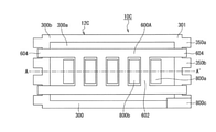
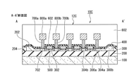
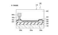
- FIG. 6 is a cross-sectional view taken along the line AA'of the semiconductor device shown in FIG. 26.
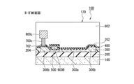
- FIG. 6 is a cross-sectional view taken along the line BB'of the semiconductor device shown in FIG. 26.
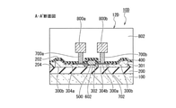
- FIG. 9 is a cross-sectional view taken along the line BB'of the semiconductor device shown in FIG. 29.
- the "first conductive type” means one of the p-type and the n-type
- the "second conductive type” means one of the p-type or the n-type different from the "first conductive type”.
- “+” and “-” attached to "n” and “p” are semiconductors having a relatively high or low impurity density, respectively, as compared with the semiconductor regions to which "+” and “-” are not added. It means that it is an area. However, even in the semiconductor regions with the same "n” and "n”, it does not mean that the impurity densities of the respective semiconductor regions are exactly the same.
- the definition of the vertical direction in the following description is merely a definition for convenience of explanation, and does not limit the technical idea of the present disclosure.
- the top and bottom are converted to left and right and read, and if the object is rotated by 180 ° and observed, the top and bottom are reversed and read.
- the effects described in the present specification are merely examples and are not limited, and other effects may be used.
- FIG. 1 is a plan view of the semiconductor device 10 according to the first embodiment of the present disclosure.
- the transistor 12 is an n-type MOS-FET, and an H-shaped gate electrode structure is described in its planar structure.
- the transistor 12 in the first embodiment is not limited to such an example, and may be a transistor having another configuration.
- an embedded insulating film 200 (see FIGS. 2 to 4) is provided on a silicon support substrate 100 which is a high resistance silicon having a resistivity of 500 ⁇ cm or more. Further, an impurity diffusion layer (semiconductor layer) 300 is provided on the embedded insulating film 200.
- the impurity diffusion layer 300 is provided with a transistor 12. Specifically, as shown in FIG. 1A, on the impurity diffusion layer 300, two gate electrode wiring portions 600 and a gate electrode portion 602 constituting the gate electrode, a source electrode 800a, and a drain electrode 800b And a body contact electrode 800c are provided.
- the two gate electrode wiring portions 600 and the gate electrode portion 602 provided on the impurity diffusion layer 300 are made of polysilicon and have an H-shaped shape that is tilted sideways when viewed from above the silicon support substrate 100.
- the gate electrode portion 602 is a rectangular electrode portion located in the center of FIG. 1A and extending along the vertical direction in the drawing.
- the two gate electrode wiring portions 600 are two strip-shaped wirings extending in the left-right direction in FIG. 1A so as to sandwich the rectangular gate electrode portion 602 in the central portion from the vertical direction in the drawing. It is a department. Further, the two gate electrode wiring portions 600 are connected to the gate electrode portion 602 at the center.
- the gate electrode wiring portion 600 extends on the impurity diffusion layer 300 from the central portion thereof along the left-right direction in the figure, and further.
- a gate electrode wiring lead-out portion 604 is formed along the left-right direction in the figure beyond the end portion 301 of the transistor 12.
- a source electrode 800a made of a metal film and a drain electrode 800b are provided so as to sandwich the gate electrode portion 602 located at the center of the impurity diffusion layer 300 from the left and right.
- the source electrode 800a and the drain electrode 800b function as wiring connected to the source region and the drain region of the transistor 12.
- the impurity diffusion layer 300 is made of a silicon layer into which a desired impurity is injected. Specifically, as shown in FIG. 1B, the source N + region 305a in which n-type impurities such as phosphorus and arsenic are diffused is located below and around the source electrode 800a and the drain electrode 800b of the impurity diffusion layer 300. And the drain N + region 305b is formed, and p-type impurities such as boron are diffused in other regions of the impurity diffusion layer 300.
- a body contact electrode 800c is provided in the lower right of the impurity diffusion layer 300.
- the body contact electrode 800c is used as wiring for fixing and controlling the potential of the impurity diffusion layer 300 in order to suppress the substrate floating effect.
- STI204 in which an insulating film such as a silicon oxide film is embedded is provided so as to surround the periphery of the impurity diffusion layer 300, and the transistor 12 provided in the impurity diffusion layer 300 is made of silicon. It is separated from other elements provided on the support substrate 100.
- the impurity diffusion layer 300 from the side surface of the impurity diffusion layer 300 made of the silicon layer 320 of the semiconductor substrate in the vicinity of the portion where the gate electrode wiring portion 600 and the end portion 301 of the transistor 12 of the impurity diffusion layer 300 intersect. Two protrusions 350a and 350b formed of a part of the impurity diffusion layer 300 protruding outward are formed.
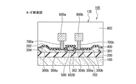
- FIG. 2 is a cross-sectional view taken along the line AA'and aa'of the semiconductor device 10 shown in FIG. 1 (a)
- FIG. 3 is a cross-sectional view taken along the line BB of the semiconductor device 10 shown in FIG. 1 (a).
- It is a cross-sectional view in ′
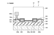
- FIG. 4 is a cross-sectional view in CC ′ of the semiconductor device 10 shown in FIG. 1 (a).
- the semiconductor device 10 is an embedded insulating film made of a silicon oxide film provided on a silicon support substrate 100 made of high-resistance silicon, as described above. It has a film 200. Further, the semiconductor device 10 has an impurity diffusion layer 300 made of a silicon layer provided on the embedded insulating film 200. That is, in the first embodiment, the above-mentioned SOI substrate is used as the substrate, and the impurity diffusion layer 300 corresponds to the above-mentioned SOI layer. In the first embodiment, the parasitic capacitance in the transistor 12 can be reduced by using the SOI substrate.
- the back surface of the silicon support substrate 100 may be ground to form a thin film after the semiconductor device 10 is manufactured, and the film thickness of the silicon support substrate 100 is not particularly limited.
- the embedded insulating film 200 has a film thickness of about 100 nm to 2000 nm, and preferably has a film thickness of about 400 nm in consideration of the high frequency characteristics of the transistor 12.
- the impurity diffusion layer 300 has a thin film portion 300a in the central portion and a thick film portion 300b having a thicker film thickness than the thin film portion 300a at the end portion 301 of the transistor 12. .. Further, the impurity diffusion layer 300 has a thick film portion 300b having the same film thickness as the end portion 301 of the transistor 12 on the protrusions 350a and 350b (only the protrusion 350b is shown in FIG. 2). The protrusions 350a and 350b protrude from the end 301 of the transistor 12 of the impurity diffusion layer 300 by, for example, 0.4 ⁇ m or more (indicated by ⁇ W in FIG. 2).
- the central portion of the thin film portion 300a located below the gate electrode portion 602 corresponds to the gate region 302 of the transistor 12 in which p-type impurities are diffused. Further, the region of the thin film portion 300a that sandwiches the gate region 302 from the left and right in the figure corresponds to the source region 304a and the drain region 304b in which n-type impurities are diffused.
- the source region 304a and the drain region 304b adjacent to the gate region 302 form the LDD layer 2000 having an impurity concentration lower than that in the source region 304a and the drain region 304b located away from the gate region 302. Is desirable. Details will be described with reference to FIG. 19 described later.
- the thick film portion 300b located at the end portion 301 of the impurity diffusion layer 300 is thicker than the thin film portion 300a located at the central portion of the impurity diffusion layer 300, and more specifically, the thin film portion 300a 2 It has a film thickness of 2 to 10 times. More specifically, in consideration of compatibility between the high frequency characteristics of the transistor 12 and reliability, the film thickness of the thick film portion 300b is preferably 140 nm to 200 nm, and the film thickness of the thin film portion 300a is 20 nm to 20 nm. It is preferably 70 nm.
- the thin film portion located in the central portion of the impurity diffusion layer 300 is designated as 300a
- the thick film portion located at the end portion 301 of the impurity diffusion layer 300 is designated as 300a. It is shown as 300b.
- the gate insulating film 500 is provided on the gate region 302 provided in the central portion of the impurity diffusion layer 300.
- the gate insulating film 500 is formed of a silicon oxide film, and the film thickness thereof can be arbitrarily selected.
- silicide films 702 are provided on the upper surface of the impurity diffusion layer 300 located on both sides of the gate region 302, separated from the gate region 302. Further, a source contact via 700a and a source electrode 800a, and a drain contact via 700b and a drain electrode 800b are provided on the silicide film 702, respectively. That is, the source contact via 700a and the drain contact via 700b are on the source region 304a and the drain region 304b formed in the thin film portion 300a of the impurity diffusion layer 300, and the gate electrode portion 602 is on the source region 304a and the drain region 304b. It is provided so as to be sandwiched between them.
- the silicide film 702 is a compound film of silicon and other elements, and the source contact via 700a, the drain contact via 700b, the source electrode 800a, and the drain electrode 800b are formed of a metal film or the like.
- the film thickness, size, and shape of the source region 304a, drain region 304b, silicide film 702, source contact via 700a, drain contact via 700b, source electrode 800a, and drain electrode 800b. Etc. are not particularly limited. Further, in the first embodiment, in order to maintain a high manufacturing yield of the semiconductor device 10, it is preferable to lay out the transistor 12 in consideration of manufacturing variations and the like.
- the source contact via 700a and the drain contact via 700b are provided on the thin film portion 300a of the impurity diffusion layer 300 in order to reduce the parasitic capacitance between the source and the drain.
- an STI (separation insulating film) 204 is provided around the impurity diffusion layer 300 in order to separate the transistor 12 from other elements.
- the STI 204 has a trench provided so as to surround the periphery of the impurity diffusion layer 300, and a silicon oxide film embedded in the trench.
- the width, depth, shape, etc. of the trench of STI204 are not particularly limited.
- a silicon oxide film 202 is provided so as to cover the gate electrode portion 602, the impurity diffusion layer 300, and the STI 204. Further, a further silicon nitride film 400 is provided so as to cover the silicon oxide film 202. In addition, a silicon oxide film 802 is provided on the silicon nitride film 400 between the source contact via 700a and the drain contact via 700b, and between the source electrode 800a and the drain electrode 800b. In the first embodiment, the material, film thickness, and the like of the silicon oxide film 202, the silicon nitride film 400, and the silicon oxide film 802 are not particularly limited.
- the semiconductor device 10 is provided on the silicon support substrate 100, the embedded insulating film 200 provided on the silicon support substrate 100, and the embedded insulating film 200. It has an impurity diffusion layer 300.
- the impurity diffusion layer 300 has a thin film portion 300a at the center and a thick film portion 300b at the end 301 of the transistor 12, as in the cross section of FIG. Have.
- the thick film portion 300b has a film thickness 2 to 10 times that of the thin film portion 300a, and more specifically, the film thickness of the thick film portion 300b is 140 nm to 200 nm.
- the film thickness of the thin film portion 300a is preferably 20 nm to 70 nm.
- a gate electrode wiring portion 600 is provided on the thin film portion 300a and the thick film portion 300b of the impurity diffusion layer 300 via the gate insulating film 500. As shown in FIG. 3, the gate electrode wiring portion 600 extends in the left-right direction in the figure on the impurity diffusion layer 300, and further extends beyond the end portion 301 of the transistor 12 in the left-right direction in the figure. The portion 604 is formed. That is, the gate electrode wiring portion 600 is provided so as to pass not only on the thin film portion 300a of the impurity diffusion layer 300 but also on the thick film portion 300b.
- the cross section is a cross section obtained when the body contact electrode 800c is cut across the body contact electrode 800c.
- the semiconductor device 10 is a silicon support substrate 100, an embedded insulating film 200 provided on the silicon support substrate 100, and impurities provided on the embedded insulating film. It has a diffusion layer 300 and the like.
- the impurity diffusion layer 300 has a thin film portion 300a at the center and a thick film portion 300b at the end 301 of the transistor 12, as in the cross section of FIG. Have.
- the thick film portion 300b has a film thickness 2 to 10 times that of the thin film portion 300a, and more specifically, the film thickness of the thick film portion 300b is 140 nm to 200 nm.
- the film thickness of the thin film portion 300a is preferably 20 nm to 70 nm.
- a gate electrode wiring portion 600 is provided on the thin film portion 300a of the impurity diffusion layer 300 via the gate insulating film 500.
- a body contact via 700c and a body contact electrode 800c are provided on the upper surface of the thick film portion 300b via the silicide film 702.
- the silicide film 702 is a compound film of silicon and other elements, and the body contact via 700c and the body contact electrode 800c are formed of a metal film or the like.
- the film thickness, size, shape and the like of the silicide film 702, the body contact via 700c and the body contact electrode 800c are not particularly limited.
- the source contact via 700a and the drain contact via 700b are provided on the thin film portion 300a of the impurity diffusion layer 300, thereby reducing the parasitic capacitance between the source and the drain. is doing.
- the body contact via 700c is provided on the thick film portion 300b of the impurity diffusion layer 300. Since the parasitic capacitance between the body (impurity diffusion layer 300) and the gate has a small effect on the high frequency characteristics of the transistor 12, the body contact via 700c is on the thick film portion 300b of the impurity diffusion layer 300. It may be provided in.
- an embedded insulating film 200 made of a silicon oxide film and having a film thickness of 100 nm to 2000 nm, preferably 400 nm is formed on a silicon support substrate 100. Further, an SOI substrate having a silicon layer 320 having a film thickness of 30 nm to 400 nm, preferably 175 nm, is used on the embedded insulating film 200.
- the upper surface of the silicon layer 320 is subjected to an oxidation treatment to form a silicon oxide film 900 having a film thickness of 10 nm to 100 nm, preferably 10 nm.
- the above-mentioned oxidation treatment method is not particularly limited, and various known oxidation treatment methods can be used.
- a silicon nitride film 902 having a film thickness of 10 nm to 300 nm, preferably 100 nm is formed on the silicon oxide film 900 by CVD (Chemical Vapor Deposition).
- the resist pattern 904 has a pattern having an opening at a position where the film thickness of the silicon layer 320 is reduced.
- the pattern is a region in which the film thickness gradually changes located between the thin film portion (corresponding to the above-mentioned thin film portion 300a) and the thick film portion (corresponding to the above-mentioned thick film portion 300b) of the silicon layer 320. It is preferable that the layout pattern is designed so that the length, that is, the distance between the thin film portion and the thick film portion is about 400 nm.
- the silicon nitride film 902 and the silicon oxide film 900 are dry-etched using the resist pattern 904 as a mask.
- the resist pattern 904 is removed after obtaining the opening 906 in which a part of the upper surface of the silicon layer 320 is exposed.
- the silicon oxide film 900 is subjected to the dry etching process, a part of the upper surface of the silicon layer 320 exposed from the opening 906 may be etched.
- a selective oxidation treatment (LOCal Oxidation of Silicon; LOCOS oxidation treatment) is performed on a part of the silicon layer 320 exposed from the opening 906.
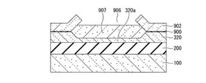
- the amount of oxidation in which the silicon layer 320 is oxidized by the oxidation treatment is controlled so that the film thickness of the silicon layer 320 located at the opening 906 becomes a desired film thickness. More specifically, when the film thickness of the central portion 320a of the silicon layer 320 (that is, the film thickness of the thin film portion 300a of the impurity diffusion layer 300) is finally set to 60 nm, in the step of FIG. It is preferable to control the film thickness of the silicon layer 320 located at the opening 906 to be about 80 nm.
- the silicon layer 320 is partially thinned. Subsequently, when the silicon nitride film 902 is removed with phosphoric acid and the silicon oxide film 900 is further removed with phosphoric acid or the like, the silicon thin film portion 908 in which the silicon layer 320 is partially thinned as shown in FIG. 10 is obtained. The silicon layer 320 having can be obtained.
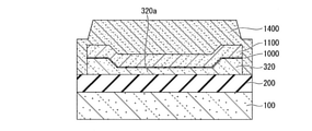
- the upper surface of the silicon layer 320 is oxidized to form a silicon oxide film 1000 having a film thickness of 10 nm to 100 nm, preferably 10 nm, on the silicon layer 320.
- a silicon nitride film 1100 having a film thickness of 10 nm to 400 nm, preferably 210 nm is formed by using CVD.
- a resist is applied to the entire surface of the silicon nitride film 1100 and exposed using photolithography to form a resist pattern 1300.
- the resist pattern 1300 has a pattern having an opening at a position forming an STI 204 for separating the transistor 12 from other elements.
- the resist pattern 1300 has resist patterns 350a', 350b having protrusions so that silicon near the region where the end 301 of the transistor 12 and the gate electrode wiring portion 600 intersect each other protrudes. 'Is included in the resist pattern 1300 for element separation, so that an increase in the number of photolithography steps is suppressed.
- the silicon nitride film 1100 and the silicon oxide film 1000 are dry-etched using the resist pattern 1300 as a mask. Further, after exposing the upper surface of the silicon layer 320 in a portion not covered by the resist pattern 1300, the resist pattern 1300 is removed.
- the method for removing the resist pattern 1300 is not particularly limited, and various known removal methods such as ashing can be used. Then, the structure shown in FIG. 12 can be obtained by etching the silicon layer 320 with the silicon nitride film 1100 as a mask by the dry etching process under the conditions different from the above.
- the entire upper part of the silicon support substrate 100 is embedded so that the inside of the trenches provided on both sides of the silicon layer 320 is embedded by the silicon oxide film 1400.
- a silicon oxide film 1400 is formed on the surface.
- the silicon oxide film 1400 may be formed so as to cover the upper surface of the silicon nitride film 1100, and the film thickness of the silicon oxide film 1400 is formed to be 50 nm to 1000 nm, preferably 400 nm.
- a resist film 1500 is formed by applying a resist to the entire surface of the silicon oxide film 1400 and exposing it using photolithography.
- the resist film 1500 has a pattern having an opening 1600 at a position corresponding to the removed silicon oxide film 1400 and the silicon nitride film 1100 located on the central portion 320a of the silicon layer 320. At this time, it is preferable that the opening 1600 extends above the central portion 320a of the silicon layer 320, and further extends to the thick film portion of the silicon layer 320 at the end portion 320b of the silicon layer 320. ..
- the silicon oxide film 1400 is removed by performing a dry etching process on the silicon oxide film 1400 using the resist film 1500 as a mask. By doing so, the structure shown in FIG. 14 can be obtained.
- CMP Chemical Mechanical Polishing
- the film thickness of the central portion 320a and the silicon layer 320 between the central portion 320a and the end portion 320b gradually changes above the region.
- the silicon oxide film 1400 remains on the surface. Therefore, in order to avoid such residual silicon oxide film 1400, it is preferable to carry out the above-mentioned dry etching process under overetching conditions to the extent that the silicon nitride film 1100 is also etched.
- the resist film 1500 is removed. Further, the upper surface of the silicon support substrate 100 is subjected to a flattening treatment using CMP to obtain the structure shown in FIG.
- the flattened silicon oxide film 1400 forms an STI 204 for element separation.
- the transistor forming region 1700 as shown in FIG. 17 can be obtained.
- impurities may be implanted into the transistor forming region 1700 by, for example, ion implantation. At this time, impurities may be injected into a desired portion of the transistor forming region 1700 by covering the upper surface of the transistor forming region 1700 with a patterned resist.
- a gate insulating film 500 made of a silicon oxide film is formed on the transistor forming regions 1700 and STI204. Further, as shown in FIG. 18, a polysilicon film is formed on the entire surface of the gate insulating film 500, and the polysilicon film is patterned into an arbitrary shape by etching or the like to form a gate electrode portion 602. To form. Subsequently, the impurity diffusion layer 300 is formed by implanting impurities into the transistor formation region 1700 by ion implantation using the gate electrode portion 602 as a mask.
- a desired impurity is implanted around the gate region 302 of the impurity diffusion layer 300 so that the impurity concentration is lower than that of the above-mentioned ion implantation, and the LDD (Lightly Doped Drain) layer 2000 is placed in the impurity diffusion layer 300.
- the LDD layer 2000 the above-mentioned ion implantation may be performed.
- the gate insulating film 500 is patterned by etching using the gate electrode portion 602 as a mask.
- the silicide film 702 may be formed on the upper surface of the exposed impurity diffusion layer 300 at a position separated from the gate electrode portions 602 on both sides of the gate electrode portion 602.
- the method for forming the above-mentioned silicide film 702 is not particularly limited, and various known forming methods can be used.
- the silicon oxide film 202, the silicon nitride film 400, and the silicon oxide film 802 are sequentially formed on the impurity diffusion layer 300, the STI 204, and the gate electrode portion 602.
- the source contact via 700a and the drain contact via 700b that penetrate the silicon nitride film 400 and the silicon oxide film 202 and reach the silicide film 702 are formed from the silicon oxide film 802.
- the source contact via 700a and the drain contact via 700b can be provided on the wide thin film portion 300a at a distance of a predetermined distance. Therefore, since it is possible to avoid patterning the source contact via 700a and the drain contact via 700b with high accuracy, it is possible to avoid a decrease in the manufacturing yield.
- the source contact via 700a and the drain contact via 700b can be provided apart from each other by a predetermined distance, the increase in the layout size of the transistor is suppressed and the manufacturing cost is increased, particularly in the transistor having a plurality of gates. Can be suppressed.
- the source electrode 800a is formed on the source contact via 700a
- the drain electrode 800b is formed on the drain contact via 700b.
- the method for forming the above-mentioned silicon oxide film 202, silicon nitride film 400, silicon oxide film 802, source contact via 700a, drain contact via 700b, source electrode 800a, and drain electrode 800b is not particularly limited.
- a forming method generally used in the method for manufacturing the semiconductor device 10 can be used.
- a further metal film may be formed on the source electrode 800a and the drain electrode 800b. In this way, the semiconductor device 10 according to the embodiment of the present disclosure shown in FIGS. 1 to 4 can be obtained.
- FIG. 21 shows a plane of the semiconductor device 10 as a comparative example.
- the same parts as those in FIG. 1 are designated by the same reference numerals, and detailed description thereof will be omitted.
- the impurity diffusion layer 300 of the gate electrode wiring extraction portion 604 is susceptible to physical damage (microcracks, etc.) in the CMP step at the time of STI formation, and the gate is easily subjected to the subsequent thermal oxidation step. There is a problem that a gate leak defect occurs due to deterioration of the film quality of the insulating film 500 and deterioration of the withstand voltage against an electric field.
- the silicon layer 320 of the semiconductor substrate is located in the vicinity of the portion where the gate electrode wiring portion 600 and the end portion 301 of the impurity diffusion layer 300 intersect.
- Two protrusions 350a and 350b are formed so as to project outward from the side surface of the impurity diffusion layer 300 made of the same material.
- the two protrusions 350a and 350b have a length of 0.4 ⁇ m or more in the direction parallel to the stretching direction of the gate electrode wiring portion 600 and 0.7 ⁇ m or more in the vertical direction. It should be noted that it is preferably 1 ⁇ m or more in the parallel direction and 1 ⁇ m or more in the vertical direction.
- the distances between the two protrusions 350a and 350b from the gate electrode wiring lead-out portion 604 are 14 nm or more and 200 nm or less.
- the impurity diffusion layer 300 is formed by the amount of the protrusions 350a and 350b.
- the region where the end portion 301 of the impurity diffusion layer 300 and the gate electrode wiring portion 600 intersect is protected from CMP damage, and gate leakage is prevented.
- the distance between the protrusions 350a and 350b and the gate electrode wiring lead-out portion 604 is set to 14 nm or more and 200 nm or less. It is possible to suppress the increase in manufacturing cost by preventing the increase of unnecessary gate parasitic capacitance and ensuring high reliability and high yield by suppressing dust generation because no material remains.
- FIG. 22 shows a plane of the semiconductor device 10A as a first modification of the first embodiment of the present disclosure.
- the same parts as those in FIG. 1A are designated by the same reference numerals, and detailed description thereof will be omitted.
- the transistor 12A forms a gate electrode portion 602 and a gate electrode wiring lead-out portion 604, which is a lead-out portion of the gate electrode wiring portion 600. Further, the transistor 12A is one that projects outward from the side surface of the impurity diffusion layer 300 made of the silicon layer 320 of the semiconductor substrate in the vicinity of the portion where the gate electrode wiring portion 600 and the end portion 301 of the transistor 12A intersect.
- the protrusion 350a is formed.
- the protrusions 350a are provided on the opposite side to the end of the gate electrode wiring extraction portions 604 facing each other, that is, on the outside. I try to form it. Even in such a first modification, the same effect as that of the first embodiment can be obtained.
- FIG. 23 shows a plane of the semiconductor device 10B as a second modification of the first embodiment of the present disclosure.
- the same parts as those in FIG. 1A are designated by the same reference numerals, and detailed description thereof will be omitted.
- the transistor 12B is arranged from the side surface of the impurity diffusion layer 300 made of the silicon layer 320 of the semiconductor substrate to the outside in the vicinity of the portion where the gate electrode wiring portion 600 and the end portion 301 of the transistor 12B intersect.
- Two protruding protrusions 351a and 351b are formed.
- the two protrusions 351a and 351b have a round shape when viewed from above the transistor 12B.
- the two protrusions 352a and 352b are triangular when viewed from above the transistor 12B.
- the two protrusions 353a and 353b are triangles having different orientations from those in FIG. 23 (b).
- the two protrusions 354a and 354b are polygonal when viewed from above the transistor 12B. Even in such a second modification, the same effect as that of the first embodiment can be obtained.
- FIG. 24 shows a plane of the semiconductor device 10C as the second embodiment of the present disclosure.
- FIG. 23 the same parts as those in FIG. 1A are designated by the same reference numerals, and detailed description thereof will be omitted.
- FIG. 25 is a cross-sectional view taken along the line AA ′ of the semiconductor device 10C shown in FIG. 24.
- the same parts as those in FIG. 2 are designated by the same reference numerals, and detailed description thereof will be omitted.
- the semiconductor device 10C and the transistor 12C have a plurality of ladder-shaped gate electrode portions 602 and two gate electrode wiring portions 600A when viewed from above the silicon support substrate 100.
- the plurality of gate electrode portions 602 are arranged along the left-right direction in FIG. 24.
- the two gate electrode wiring portions 600A sandwich the plurality of gate electrode portions 602 along the vertical direction in FIG. 24, and connect the plurality of gate electrode portions 602 to each other.
- a source electrode 800a and a drain electrode 800b are provided so as to sandwich each gate electrode portion 602 from the left-right direction in FIG. 24.
- the semiconductor device 10C and the transistor 12C project outward from the side surface of the impurity diffusion layer 300 made of the silicon layer 320 of the semiconductor substrate in the vicinity of the portion where the gate electrode wiring portion 600A and the end portion 301 of the transistor 12C intersect.
- the two protrusions 350a and 350b are formed.
- the gate electrode wiring portion 600A forms a gate electrode wiring extraction portion 604 beyond the end portion 301 of the transistor 12C.
- the impurity diffusion layer 300 is located at the thin film portion 300a located in the central portion and the end portion 301, as in the first embodiment described above. It has a thick film portion 300b to be formed. Also in the second embodiment, the gate region 302, the source region 304a, and the drain region 304b are provided in the thin film portion 300a of the impurity diffusion layer 300. As described above, even when a plurality of gate regions 302 are provided, the impurity diffusion layer 300 having the thin film portion 300a and the thick film portion 300b can be applied. Even in such a second embodiment, the same effect as that of the first embodiment can be obtained.
- FIG. 26 shows a plane of the semiconductor device 10D as the third embodiment of the present disclosure.
- the same parts as those in FIG. 1A are designated by the same reference numerals, and detailed description thereof will be omitted.
- FIG. 27 is a cross-sectional view taken along the line AA of the semiconductor device 10D shown in FIG. 26.
- the same parts as those in FIG. 2 are designated by the same reference numerals, and detailed description thereof will be omitted.
- FIG. 28 is a cross-sectional view taken along the line BB'of the semiconductor device 10D shown in FIG.
- the same parts as those in FIG. 4 are designated by the same reference numerals, and detailed description thereof will be omitted.
- the semiconductor device 10D has a gate electrode wiring portion 600B and a gate electrode portion 602A having a T-shape when viewed from above the silicon support substrate 100. ing.
- the gate electrode portion 602A has a rectangular shape extending along the vertical direction in FIG. 26.
- the gate electrode wiring portion 600B is a rectangular wiring portion extending along the left-right direction in FIG. 26.
- a source electrode 800a and a drain electrode 800b are provided so as to sandwich the gate electrode portion 602A from the left-right direction in FIG. 26.
- the semiconductor device 10D and the transistor 12D project outward from the side surface of the impurity diffusion layer 300 made of the silicon layer 320 of the semiconductor substrate in the vicinity of the portion where the gate electrode wiring portion 600B and the end portion 301 of the transistor 12D intersect.
- the two protrusions 350a and 350b are formed.
- the semiconductor device 10D and the transistor 12D are projected outward from the side surface of the impurity diffusion layer 300 made of the silicon layer 320 of the semiconductor substrate in the vicinity of the portion where the gate electrode portion 602A and the end portion 301 of the transistor 12D intersect. It forms two protrusions 360a and 360b.
- the gate electrode portion 602A forms a gate electrode lead-out portion 605 beyond the end portion 301 of the transistor 12D.
- the impurity diffusion layer 300 is located at the thin film portion 300a located in the central portion and the end portion 301, as in the first embodiment described above. It has a thick film portion 300b to be formed. Also in the third embodiment, the gate region 302, the source region 304a, and the drain region 304b are provided in the thin film portion 300a of the impurity diffusion layer 300. As described above, even when the gate electrode wiring portion 600B and the gate electrode portion 602A having a T-shape are provided, the impurity diffusion layer 300 having the thin film portion 300a and the thick film portion 300b can be applied. Even in such a third embodiment, the same effect as that of the first embodiment can be obtained.
- FIG. 29 shows a plane of the semiconductor device 10E as the fourth embodiment of the present disclosure.
- the same parts as those in FIG. 26 are designated by the same reference numerals, and detailed description thereof will be omitted.
- FIG. 30 is a cross-sectional view taken along the line AA of the semiconductor device 10E shown in FIG. 29.
- the same parts as those in FIG. 2 are designated by the same reference numerals, and detailed description thereof will be omitted.
- FIG. 31 is a cross-sectional view taken along the line BB'of the semiconductor device 10E shown in FIG. 29.
- the same parts as those in FIG. 4 are designated by the same reference numerals, and detailed description thereof will be omitted.
- the semiconductor device 10E has an I-shaped gate electrode portion 602B when viewed from above the silicon support substrate 100.
- the gate electrode portion 602B has a rectangular shape extending along the vertical direction in FIG. 29.
- a source electrode 800a and a drain electrode 800b are provided so as to sandwich the gate electrode portion 602B from the left-right direction in FIG. 29.
- the semiconductor device 10E and the transistor 12E are projected outward from the side surface of the impurity diffusion layer 300 made of the silicon layer 320 of the semiconductor substrate in the vicinity of the portion where the gate electrode portion 602B and the end portion 301 of the transistor 12E intersect. It forms two protrusions 360a and 360b. Further, the gate electrode portion 602B extends beyond the end portion 301 of the transistor 12E to form a gate electrode lead-out portion 605.
- the impurity diffusion layer 300 has a thin film portion 300a located at the central portion and a thick film portion 300b located at the end portion 301, as in the first embodiment described above.
- the gate region 302, the source region 304a, and the drain region 304b are provided in the thin film portion 300a of the impurity diffusion layer 300.
- the impurity diffusion layer 300 having the thin film portion 300a and the thick film portion 300b can be applied. Even in such a fourth embodiment, the same effect as that of the first embodiment can be obtained.
- the present disclosure may also have the following structure.
- a substrate having an embedded insulating film and a semiconductor layer provided on the embedded insulating film and on which a semiconductor element is formed.
- a gate electrode provided on the semiconductor layer and having wiring extending from the central portion of the semiconductor layer to the end portion of the semiconductor layer when the substrate is viewed from above.
- Source contact vias and drain contact vias provided on the semiconductor layer, In the vicinity of the region where the end of the semiconductor layer and the wiring of the gate electrode intersect, a protrusion formed of the same material as the semiconductor layer and protruding outward from the side surface of the semiconductor layer, Equipped with The end portion of the semiconductor layer has at least a part of a thick film region thicker than the film thickness immediately below the gate electrode of the semiconductor layer.
- the source contact via and the drain contact via are provided in a region other than the thick film region.
- (2) The wiring has a lead-out portion extending outward from the end portion of the semiconductor layer.
- (3) The wiring has a lead-out portion extending outward from the end portion of the semiconductor layer.
- a plurality of drawer portions of the gate electrode are arranged in parallel, and the drawer portions are arranged in parallel.
- the protrusion is provided at an end opposite to the end where the drawers of the gate electrodes face each other.
- the end portion of the semiconductor layer has a film thickness of 2 to 10 times the film thickness of the central portion of the semiconductor layer.
- the film thickness of the end portion of the semiconductor layer is 140 nm to 200 nm.
- the film thickness of the central portion of the semiconductor layer is 20 nm to 70 nm.
- the protrusion is 0.4 ⁇ m or more in the direction parallel to the extending direction of the wiring of the gate electrode, 0.7 ⁇ m or more in the vertical direction, or 1 ⁇ m or more in the parallel direction, and 1 ⁇ m or more in the vertical direction.
- the distance between the protrusion and the lead-out portion of the gate electrode is 14 nm or more and 200 nm or less.
- the protrusion has at least one shape of a quadrangle, a circle, a triangle, and a polygon when viewed from above the substrate.
- the gate electrode has an H-shaped, T-shaped, I-shaped, or ladder-shaped shape when viewed from above the substrate.
- the semiconductor device according to any one of (1) to (3). (11) When the substrate having the embedded insulating film and the semiconductor layer provided on the embedded insulating film and on which the semiconductor element is formed is viewed from above, from the central portion of the semiconductor layer to the end portion of the semiconductor layer.
- a gate electrode having extremely stretched wiring in the semiconductor layer In the vicinity of the region where the end of the semiconductor layer and the wiring of the gate electrode intersect, a protrusion protruding outward from the side surface of the semiconductor layer is formed of the same material as the semiconductor layer.
- the film thickness at the end of the semiconductor layer is made thicker than the film thickness directly under the gate electrode of the semiconductor layer.
Landscapes
- Insulated Gate Type Field-Effect Transistor (AREA)
- Thin Film Transistor (AREA)
- Electrodes Of Semiconductors (AREA)
- Metal-Oxide And Bipolar Metal-Oxide Semiconductor Integrated Circuits (AREA)
Abstract
寄生容量を低減しつつ、高い信頼性を確保し、製造コストの増加を抑えながら、ゲートリーク不良を防止できる半導体装置を提供する。半導体装置は、埋込絶縁膜と、埋込絶縁膜上に設けられ、半導体素子が形成される半導体層とを有する基板と、半導体層上に設けられ、基板を上方から見た場合に、半導体層の中央部から半導体層の端部に至り延伸した配線を有するゲート電極と、半導体層上に設けられるソースコンタクトビア及びドレインコンタクトビアと、半導体層の端部とゲート電極の配線とが交差する領域の近傍に、半導体層と同一の材料で形成され前記半導体層の側面から外側へ突出する突起部とを備える。半導体層の端部は、少なくとも一部に半導体層のゲート電極直下の膜厚に比べて厚い厚膜領域を有する。ソースコンタクトビア及びドレインコンタクトビアは、厚膜領域以外の領域に設けられる。
Description
本開示(本技術)は、半導体装置、及び半導体装置の製造方法に関する。
無線通信等に用いられる通信装置においては、高周波通信信号を切り替える高周波アンテナスイッチが設けられている。このような高周波アンテナスイッチにおいては、取り扱う信号が高周波であってもデバイス特性が劣化しない、寄生容量の小さなデバイスであることが求められる。
そこで、従来、アンテナスイッチ用デバイスとしては、高周波特性が良いGaAs(ガリウム砒素)のような化合物半導体が用いられていた。しかしながら、このような化合物半導体デバイスは高価であり、化合物半導体デバイスを動作させるための周辺回路用デバイスが化合物半導体デバイスとは異なる別のチップ上に作成されることから、モジュール等に組み込む際の製造コストを抑えることが難しい。
そこで、近年、アンテナスイッチ用デバイスと、周辺回路用デバイスとを混載して同一のチップ上に作成可能なSOI(SiliconOnInsulator)基板を用いたアンテナスイッチIC(IntegratedCircuit)の開発が盛んになっている。SOI基板は、高抵抗支持基板の上に設けられた埋込絶縁膜(BOX層)と、当該埋込絶縁膜上にシリコンからなる半導体層(SOI層)とを有する基板のことをいう。このようなSOI基板を用いることにより、PN接合領域に生じる空乏層による寄生容量を低減することができることから、高周波特性の劣化が生じにくく、上述した化合物半導体と同等のデバイス特性を持つアンテナスイッチ用デバイスを作成することができる。さらには、このようなSOI基板を用いてアンテナスイッチ用デバイスを作成した場合には、同一基板上に周辺回路用デバイスを混載して形成することができる。なお、このようなSOI基板に作成されたデバイスの例としては、下記の特許文献1に開示の半導体装置を挙げることができる。
しかしながら、半導体装置の製造工程において実施される熱酸化やエッチング、研磨等の処理により、SOI層が局所的に薄くなることがある。このように薄くなったSOI層の部分には、電界効果型トランジスタ(以下、FETと称する)の動作中に電界集中が生じ、当該FETの信頼性を低下させる一因となる。また、このようなFETの信頼性の低下を防ぐためにこれまで様々な対策が講じられてきたが、これら対策により、寄生容量が増加してFETの高周波特性が低下したり、製造コストが大幅に増加したりしてしまうことがあった。
これらの問題に対し、SOI層端部のみの膜厚を厚くし、低寄生容量と高信頼性、低コストを実現している下記特許文献2に挙げる技術が公開されている。
これらの問題に対し、SOI層端部のみの膜厚を厚くし、低寄生容量と高信頼性、低コストを実現している下記特許文献2に挙げる技術が公開されている。
しかしながら、上記技術であっても、FETのサイズが大きくなると、STI(Shallow Trench Isolation)形成時のCMP(Chemical Mechanical Polishing)ダメージがシリコン(Si)層に生じ、ゲートリーク不良が発生していた。
本開示はこのような事情に鑑みてなされたもので、寄生容量を低減しつつ、高い信頼性を確保し、製造コストの増加を抑えながら、ゲートリーク不良を防止できる半導体装置及び半導体装置の製造方法を提供することを目的とする。
本開示の一態様は、埋込絶縁膜と、当該埋込絶縁膜上に設けられ、半導体素子が形成される半導体層とを有する基板と、当該半導体層上に設けられ、前記基板を上方から見た場合に、前記半導体層の中央部から前記半導体層の端部に至り延伸した配線を有するゲート電極と、前記半導体層上に設けられるソースコンタクトビア及びドレインコンタクトビアと、前記半導体層の端部と前記ゲート電極の配線とが交差する領域の近傍に、前記半導体層と同一の材料で形成され前記半導体層の側面から外側へ突出する突起部と、を備え、前記半導体層の端部は、少なくとも一部に前記半導体層のゲート電極直下の膜厚に比べて厚い厚膜領域を有し、前記ソースコンタクトビア及び前記ドレインコンタクトビアは、当該厚膜領域以外の領域に設けられる半導体装置である。
本開示の他の態様は、埋込絶縁膜と、当該埋込絶縁膜上に設けられ、半導体素子が形成される半導体層とを有する基板を上方から見た場合に、前記半導体層の中央部から前記半導体層の端部に至り延伸した配線を有するゲート電極を、前記半導体層に形成することと、前記半導体層の端部と前記ゲート電極の配線とが交差する領域の近傍に、前記半導体層の側面から外側へ突出する突起部を前記半導体層と同一の材料で形成することと、前記半導体層の端部の膜厚を、前記半導体層のゲート電極直下の膜厚に比べて厚くすることとを含む半導体装置の製造方法である。
以下において、図面を参照して本開示の実施形態を説明する。以下の説明で参照する図面の記載において、同一又は類似の部分には同一又は類似の符号を付し、重複する説明を省略する。但し、図面は模式的なものであり、厚みと平面寸法との関係、各装置や各部材の厚みの比率等は現実のものと異なることに留意すべきである。したがって、具体的な厚みや寸法は以下の説明を参酌して判定すべきものである。また、図面相互間においても互いの寸法の関係や比率が異なる部分が含まれていることは勿論である。
本明細書において、「第1導電型」はp型又はn型の一方であり、「第2導電型」はp型又はn型のうちの「第1導電型」とは異なる一方を意味する。また、「n」や「p」に付す「+」や「-」は、「+」及び「-」が付記されていない半導体領域に比して、それぞれ相対的に不純物密度が高い又は低い半導体領域であることを意味する。但し、同じ「n」と「n」とが付された半導体領域であっても、それぞれの半導体領域の不純物密度が厳密に同じであることを意味するものではない。
また、以下の説明における上下等の方向の定義は、単に説明の便宜上の定義であって、本開示の技術的思想を限定するものではない。例えば、対象を90°回転して観察すれば上下は左右に変換して読まれ、180°回転して観察すれば上下は反転して読まれることは勿論である。
なお、本明細書中に記載される効果はあくまで例示であって限定されるものでは無く、また他の効果があってもよい。
なお、本明細書中に記載される効果はあくまで例示であって限定されるものでは無く、また他の効果があってもよい。
<第1の実施形態>
<平面構成>
図1は、本開示の第1の実施形態に係る半導体装置10の平面図である。なお、以下に説明する本第1の実施形態においては、トランジスタ12はn型のMOS-FETであるとし、その平面構造においてはH字型のゲート電極構造をものとして説明する。しかしながら、本第1の実施形態におけるトランジスタ12は、このような例に限定されるものではなく、他の構成を持つトランジスタであってもよい。
<平面構成>
図1は、本開示の第1の実施形態に係る半導体装置10の平面図である。なお、以下に説明する本第1の実施形態においては、トランジスタ12はn型のMOS-FETであるとし、その平面構造においてはH字型のゲート電極構造をものとして説明する。しかしながら、本第1の実施形態におけるトランジスタ12は、このような例に限定されるものではなく、他の構成を持つトランジスタであってもよい。
本第1の実施形態に係る半導体装置10においては、抵抗率が500Ωcm以上の高抵抗シリコンであるシリコン支持基板100上に、埋込絶縁膜200(図2~図4参照)が設けられており、さらに、埋込絶縁膜200上に不純物拡散層(半導体層)300が設けられる。
不純物拡散層300には、トランジスタ12が設けられる。詳細には、図1(a)に示すように、不純物拡散層300上には、ゲート電極を構成する2本のゲート電極配線部600及びゲート電極部602と、ソース電極800aと、ドレイン電極800bと、ボディコンタクト電極800cとが設けられている。不純物拡散層300上に設けられた2本のゲート電極配線部600及びゲート電極部602は、ポリシリコンから成り、シリコン支持基板100の上方から見ると横に倒したH字の形状を持つ。詳細には、ゲート電極部602は、図1(a)中の中央に位置する、図中上下方向に沿って延びる矩形状の電極部である。さらに、2本のゲート電極配線部600は、上記中央部の矩形状のゲート電極部602を図中上下方向から挟み込むように、図1(a)中左右方向に延伸する、2つの帯状の配線部である。また、上記2本のゲート電極配線部600は、中央で、上記ゲート電極部602と接続している。
さらに、図1(a)に示されるように、本実施形態においては、ゲート電極配線部600は、不純物拡散層300上を、その中央部から図中左右方向に沿って延伸しており、さらにトランジスタ12の端部301を超えて図中左右方向に沿ってゲート電極配線引き出し部604を形成している。
また、不純物拡散層300の中央に位置するゲート電極部602を左右から挟みこむように、金属膜からなるソース電極800aと、ドレイン電極800bとが設けられている。ソース電極800a及びドレイン電極800bは、トランジスタ12のソース領域及びドレイン領域と接続される配線として機能する。
また、不純物拡散層300の中央に位置するゲート電極部602を左右から挟みこむように、金属膜からなるソース電極800aと、ドレイン電極800bとが設けられている。ソース電極800a及びドレイン電極800bは、トランジスタ12のソース領域及びドレイン領域と接続される配線として機能する。
そして、不純物拡散層300は、所望の不純物が注入されたシリコン層からなる。詳細には、不純物拡散層300のソース電極800a及びドレイン電極800bの下方及びその周辺には、図1(b)に示すように、リン、ヒ素等のn型の不純物が拡散したソースN+領域305a及びドレインN+領域305bが形成されており、不純物拡散層300の他の領域には、ホウ素等のp型の不純物が拡散している。
また、図1(a)の右下に示されるように、不純物拡散層300の右下には、ボディコンタクト電極800cが設けられている。当該ボディコンタクト電極800cは、基板浮遊効果の抑制するために、不純物拡散層300の電位を固定、制御するための配線として用いられる。
また、不純物拡散層300の周囲を取り囲むように、シリコン酸化膜等の絶縁膜が埋め込まれたSTI204(図2~図4参照)が設けられ、不純物拡散層300に設けられたトランジスタ12を、シリコン支持基板100上に設けられた他の素子から分離する。
また、不純物拡散層300の周囲を取り囲むように、シリコン酸化膜等の絶縁膜が埋め込まれたSTI204(図2~図4参照)が設けられ、不純物拡散層300に設けられたトランジスタ12を、シリコン支持基板100上に設けられた他の素子から分離する。
本第1の実施形態では、ゲート電極配線部600と、不純物拡散層300のトランジスタ12の端部301とが交差する部分の近傍に、半導体基板のシリコン層320からなる不純物拡散層300の側面から外側へ突出させた不純物拡散層300の一部からなる2つの突起部350a,350bを形成している。
<断面構成>
次に、本第1の実施形態における半導体装置10の断面構成について、図2から図4を参照して説明する。図2は、図1(a)に示した半導体装置10のA-A´、a-a´における断面図であり、図3は、図1(a)に示した半導体装置10のB-B´における断面図であり、さらに、図4は、図1(a)に示した半導体装置10のC-C´における断面図である。
次に、本第1の実施形態における半導体装置10の断面構成について、図2から図4を参照して説明する。図2は、図1(a)に示した半導体装置10のA-A´、a-a´における断面図であり、図3は、図1(a)に示した半導体装置10のB-B´における断面図であり、さらに、図4は、図1(a)に示した半導体装置10のC-C´における断面図である。
図2に示すように、本第1の実施形態に係る半導体装置10は、先に説明したように、高抵抗シリコンからなるシリコン支持基板100の上に設けられたシリコン酸化膜よりなる埋込絶縁膜200を有する。さらに、半導体装置10は、埋込絶縁膜200上に設けられたシリコン層からなる不純物拡散層300を有している。すなわち、本第1の実施形態においては、基板として上述したSOI基板を用いており、不純物拡散層300が上述のSOI層に対応する。本第1の実施形態においては、SOI基板を用いていることにより、トランジスタ12における寄生容量を低減することができる。なお、シリコン支持基板100は、半導体装置10の製造後に裏面を研削して薄膜化してもよく、シリコン支持基板100の膜厚は特に限定されるものではない。また、埋込絶縁膜200は、100nm~2000nm程度の膜厚を持ち、好ましくは、トランジスタ12の高周波特性を考慮して、400nm程度の膜厚を持つことが好ましい。
不純物拡散層300は、図2に示すように、中央部に膜厚の薄い薄膜部300aと、トランジスタ12の端部301に、薄膜部300aに比べて膜厚の厚い厚膜部300bとを有する。また、不純物拡散層300は、突起部350a,350b(図2では、突起部350bのみ図示)に、トランジスタ12の端部301と同じ膜厚の厚膜部300bを有する。突起部350a,350bは、不純物拡散層300のトランジスタ12の端部301から例えば0.4μm以上(図2中、ΔWで示す)突出している。
ゲート電極部602の下に位置する当該薄膜部300aの中央部は、p型の不純物が拡散したトランジスタ12のゲート領域302にあたる。また、当該ゲート領域302を図中左右から挟み込む薄膜部300aの領域は、n型の不純物が拡散した、ソース領域304a及びドレイン領域304bにあたる。なお、ゲート領域302に隣接するソース領域304a及びドレイン領域304bは、ゲート領域302から離れて位置するソース領域304a及びドレイン領域304bにおける不純物濃度よりも、不純物濃度が薄い、LDD層2000を形成することが望ましい。詳しくは、後述の図19で説明する。
また、不純物拡散層300の端部301に位置する厚膜部300bは、不純物拡散層300の中央部に位置する薄膜部300aに対して、厚くなっており、詳細には、薄膜部300aの2倍から10倍の膜厚を持つ。より具体的には、トランジスタ12の高周波特性と信頼性との両立を考慮して、厚膜部300bの膜厚は、140nm~200nmであることが好ましく、薄膜部300aの膜厚は、20nm~70nmであることが好ましい。
なお、先に説明した図1(a)の平面図においては、不純物拡散層300の中央部に位置する薄膜部については300aとして、不純物拡散層300の端部301に位置する厚膜部については300bとして、示されている。
さらに、本実施形態に係る半導体装置10においては、不純物拡散層300の中央部に設けられたゲート領域302上にゲート絶縁膜500が設けられている。ゲート絶縁膜500は、シリコン酸化膜から形成されており、その膜厚については任意に選択することができる。
さらに、本実施形態に係る半導体装置10においては、不純物拡散層300の中央部に設けられたゲート領域302上にゲート絶縁膜500が設けられている。ゲート絶縁膜500は、シリコン酸化膜から形成されており、その膜厚については任意に選択することができる。
また、ゲート領域302の両側に位置する不純物拡散層300の上面には、ゲート領域302と離隔して2つのシリサイド膜702が設けられている。さらに、シリサイド膜702上には、それぞれソースコンタクトビア700a及びソース電極800aと、ドレインコンタクトビア700b及びドレイン電極800bとが設けられている。すなわち、ソースコンタクトビア700a、ドレインコンタクトビア700bは、不純物拡散層300の薄膜部300aに形成されたソース領域304a及びドレイン領域304bの上に、ゲート電極部602は、ソース領域304a及びドレイン領域304bの間に挟まれるように、設けられている。薄膜部300a上にソースコンタクトビア700a及びドレインコンタクトビア700bを設けることにより、ソースとドレインとの間の寄生容量を低減することができる。なお、シリサイド膜702は、シリコンと他の元素との化合物膜であり、ソースコンタクトビア700a、ドレインコンタクトビア700b、ソース電極800a及びドレイン電極800bは、金属膜等から形成される。なお、本第1の実施形態において、これら、ソース領域304a、ドレイン領域304b、シリサイド膜702、ソースコンタクトビア700a、ドレインコンタクトビア700b、ソース電極800a、ドレイン電極800bの膜厚、大きさ、及び形状等については、特に限定されるものではない。また、本第1の実施形態において、半導体装置10の製造歩留まりを高く維持するために、製造ばらつき等を考慮してトランジスタ12のレイアウトすることが好ましい。
なお、上述の説明においては、ソースとドレインとの間の寄生容量を低減するために、ソースコンタクトビア700a及びドレインコンタクトビア700bは、不純物拡散層300の薄膜部300aの上に設けられている。
また、不純物拡散層300の周囲には、トランジスタ12を他の素子から分離するために、STI(分離絶縁膜)204が設けられている。詳細には、STI204は、不純物拡散層300の周囲を囲むように設けられたトレンチと、トレンチに埋め込まれたシリコン酸化膜とを有する。なお、本実施形態においては、STI204のトレンチの幅、深さ、形状等については、特に限定されるものではない。
また、ゲート電極部602、不純物拡散層300及びSTI204を覆うように、シリコン酸化膜202が設けられている。さらに、上記シリコン酸化膜202を覆うように更なるシリコン窒化膜400が設けられている。加えて、シリコン窒化膜400上にあって、ソースコンタクトビア700aとドレインコンタクトビア700bの間、及び、ソース電極800aとドレイン電極800bとの間には、シリコン酸化膜802が設けられている。なお、本第1の実施形態において、シリコン酸化膜202、シリコン窒化膜400、シリコン酸化膜802については、その材質、膜厚等は特に限定されるものではない。
次に、図3を参照して、本第1の実施形態に係る半導体装置10を説明する。先に説明したように、当該断面図においても、半導体装置10は、シリコン支持基板100と、シリコン支持基板100上に設けられた埋込絶縁膜200と、埋込絶縁膜200上に設けられた不純物拡散層300とを有している。
図3の断面においても、不純物拡散層300は、図2の断面と同様に、中央部に膜厚の薄い薄膜部300aと、トランジスタ12の端部301に膜厚の厚い厚膜部300bとを有する。詳細には、当該断面においても、厚膜部300bは、薄膜部300aの2倍から10倍の膜厚を持ち、より具体的には、厚膜部300bの膜厚は、140nm~200nmであることが好ましく、薄膜部300aの膜厚は、20nm~70nmであることが好ましい。
また、図3の断面においては、不純物拡散層300の薄膜部300a及び厚膜部300bの上には、ゲート絶縁膜500を介してゲート電極配線部600が設けられている。図3に示すように、ゲート電極配線部600は、不純物拡散層300上を図中左右方向に延伸しており、さらに、トランジスタ12の端部301を超えて図中左右方向にゲート電極配線引き出し部604を形成している。すなわち、ゲート電極配線部600は、不純物拡散層300の薄膜部300a上だけでなく、厚膜部300b上も通過するように設けられている。
次に、図4を参照して、本第1の実施形態に係る半導体装置10を説明する。当該断面は、ボディコンタクト電極800cを横切るように切断した場合に得られる断面である。先に説明したように、当該断面図においても、半導体装置10は、シリコン支持基板100と、シリコン支持基板100上に設けられた埋込絶縁膜200と、埋込絶縁膜上に設けられた不純物拡散層300とを有している。
図4の断面においても、不純物拡散層300は、図2の断面と同様に、中央部に膜厚の薄い薄膜部300aと、トランジスタ12の端部301に膜厚の厚い厚膜部300bとを有する。詳細には、当該断面においても、厚膜部300bは、薄膜部300aの2倍から10倍の膜厚を持ち、より具体的には、厚膜部300bの膜厚は、140nm~200nmであることが好ましく、薄膜部300aの膜厚は、20nm~70nmであることが好ましい。
また、図4の断面においても、不純物拡散層300の薄膜部300aの上には、ゲート絶縁膜500を介してゲート電極配線部600が設けられている。
さらに、図4の左側に示すように、厚膜部300bの上面には、シリサイド膜702を介して、ボディコンタクトビア700cと、ボディコンタクト電極800cとが設けられている。なお、先に説明したように、シリサイド膜702は、シリコンと他の元素との化合物膜であり、ボディコンタクトビア700c及びボディコンタクト電極800cは、金属膜等から形成される。また、本第1の実施形態においては、これらシリサイド膜702、ボディコンタクトビア700c、ボディコンタクト電極800cの膜厚、大きさ、及び形状等については、特に限定されるものではない。
さらに、図4の左側に示すように、厚膜部300bの上面には、シリサイド膜702を介して、ボディコンタクトビア700cと、ボディコンタクト電極800cとが設けられている。なお、先に説明したように、シリサイド膜702は、シリコンと他の元素との化合物膜であり、ボディコンタクトビア700c及びボディコンタクト電極800cは、金属膜等から形成される。また、本第1の実施形態においては、これらシリサイド膜702、ボディコンタクトビア700c、ボディコンタクト電極800cの膜厚、大きさ、及び形状等については、特に限定されるものではない。
先に説明したように、ソースコンタクトビア700a及びドレインコンタクトビア700bは、不純物拡散層300の薄膜部300aの上に設けられており、このようにして、ソースとドレインとの間の寄生容量を低減している。一方、ボディコンタクトビア700cは、不純物拡散層300の厚膜部300bの上に設けられている。ボディ(不純物拡散層300)とゲートとの間の寄生容量については、トランジスタ12の高周波特性に対して与える影響は小さいことから、ボディコンタクトビア700cは、不純物拡散層300の厚膜部300bの上に設けてもよい。
<半導体装置の製造方法>
次に、半導体装置10の製造方法を説明する。
まず、本実施形態に係る製造方法においては、図5に示すように、シリコン支持基板100上に、シリコン酸化膜からなる、膜厚が100nm~2000nm、好ましくは400nmである埋込絶縁膜200を有し、さらに、埋込絶縁膜200上に、膜厚が30nm~400nm、好ましくは175nmのシリコン層320を有するSOI基板を使用する。
次に、半導体装置10の製造方法を説明する。
まず、本実施形態に係る製造方法においては、図5に示すように、シリコン支持基板100上に、シリコン酸化膜からなる、膜厚が100nm~2000nm、好ましくは400nmである埋込絶縁膜200を有し、さらに、埋込絶縁膜200上に、膜厚が30nm~400nm、好ましくは175nmのシリコン層320を有するSOI基板を使用する。
次に、図6に示すように、シリコン層320の上面に対して酸化処理を行うことにより、膜厚が10nm~100nm、好ましくは10nmであるシリコン酸化膜900を形成する。なお、上述の酸化処理の方法は、特に限定されるものではなく、既知の各種の酸化処理の方法を用いることができる。さらに、シリコン酸化膜900上に、CVD(Chemical Vapor Deposition)により、膜厚が10nm~300nm、好ましくは100nmであるシリコン窒化膜902を形成する。
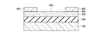
そして、図7に示すように、シリコン窒化膜902の全面にレジストを塗布し、フォトリソグラフィーを用いて露光することにより、レジストパターン904を形成する。当該レジストパターン904は、シリコン層320の膜厚を薄くする箇所に開口部を持つパターンを有する。当該パターンは、シリコン層320の薄膜部(上述の薄膜部300aに対応する)と厚膜部(上述の厚膜部300bに対応する)との間に位置する膜厚が徐々に変化する領域の長さ、すなわち、薄膜部と厚膜部との間の距離が400nm程度になるように考慮したレイアウトパターンとなっていることが好ましい。
その後、上記レジストパターン904をマスクとして用いて、シリコン窒化膜902及びシリコン酸化膜900に対してドライエッチング処理を行う。このようにして、図8に示すように、シリコン層320の上面の一部が露出した開口部906を得た後に、レジストパターン904を除去する。なお、シリコン酸化膜900に対してドライエッチング処理を施した際に、上記開口部906から露出するシリコン層320の上面の一部をエッチングしてもよい。
次に、図9に示すように、上記開口部906から露出するシリコン層320の一部に対して選択的な酸化処理(LOCal Oxidation of Silicon;LOCOS酸化処理)を行う。この際、開口部906に位置するシリコン層320の膜厚が、所望の膜厚になるように、酸化処理によりシリコン層320が酸化される酸化量を制御する。より具体的には、最終的に、シリコン層320の中央部320aの膜厚(すなわち、不純物拡散層300の薄膜部300aの膜厚)を60nmとする場合には、図9の工程においては、開口部906に位置するシリコン層320の膜厚が80nm程度になるように制御することが好ましい。このようにして、シリコン層320については部分的に薄くなる。
続いて、シリコン窒化膜902をリン酸により除去し、さらに、シリコン酸化膜900をフッ酸等により除去すると、図10に示すようなシリコン層320が部分的に薄化されたシリコン薄膜部908を有するシリコン層320を得ることができる。
続いて、シリコン窒化膜902をリン酸により除去し、さらに、シリコン酸化膜900をフッ酸等により除去すると、図10に示すようなシリコン層320が部分的に薄化されたシリコン薄膜部908を有するシリコン層320を得ることができる。
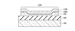
さらに、図11(a)に示すように、シリコン層320の上面を酸化処理することにより、シリコン層320上に、膜厚が10nm~100nm、好ましくは10nmであるシリコン酸化膜1000を形成する。さらに、シリコン酸化膜1000上に、CVDを用いて、膜厚が10nm~400nm、好ましくは210nmであるシリコン窒化膜1100を形成する。次いで、シリコン窒化膜1100の全面にレジストを塗布し、フォトリソグラフィーを用いて露光することにより、レジストパターン1300を形成する。当該レジストパターン1300は、トランジスタ12を他の素子から分離するためのSTI204を形成する箇所に開口部を持つパターンを有する。
このレジストパターン1300は、図11(b)に示すように、トランジスタ12の端部301とゲート電極配線部600が交差する領域付近のシリコンが突き出すように、突起部を有するレジストパターン350a’,350b’を素子分離用のレジストパターン1300に含むので、フォトリソグラフィーの工程数の増加が抑制される。
その後、レジストパターン1300をマスクとして、シリコン窒化膜1100及びシリコン酸化膜1000に対してドライエッチング処理を行う。さらに、レジストパターン1300に覆われていない箇所のシリコン層320の上面を露出させた後に、レジストパターン1300の除去を行う。なお、本実施形態においては、レジストパターン1300の除去の方法は、特に限定されるものではなく、アッシング等の既知の各種の除去方法を用いることができる。そして、上述とは異なる条件のドライエッチング処理により、シリコン窒化膜1100をマスクとしてシリコン層320をエッチングすることによって、図12に示される構造を得ることができる。
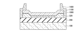
続いて、図13に示すように、HDP(High Density Plasma)等を用いて、シリコン層320の両側に設けられたトレンチ内がシリコン酸化膜1400によって埋め込まれるように、シリコン支持基板100の上方全体にシリコン酸化膜1400を形成する。この際、シリコン酸化膜1400は、シリコン窒化膜1100の上面を覆うように形成されてもよく、シリコン酸化膜1400の膜厚は、50nm~1000nm、好ましくは400nmとなるように形成される。
次に、シリコン酸化膜1400の全面にレジストを塗布し、フォトリソグラフィーを用いて露光することにより、レジスト膜1500を形成する。当該レジスト膜1500は、シリコン層320の中央部320a上に位置する除去されるシリコン酸化膜1400及びシリコン窒化膜1100に対応する箇所に開口部1600を持つパターンを有する。この際、上記開口部1600は、シリコン層320の中央部320aの上方に広がり、さらに、シリコン層320の端部320bのシリコン層320の膜厚の厚い厚膜部にまで広がっていることが好ましい。
次に、シリコン酸化膜1400の全面にレジストを塗布し、フォトリソグラフィーを用いて露光することにより、レジスト膜1500を形成する。当該レジスト膜1500は、シリコン層320の中央部320a上に位置する除去されるシリコン酸化膜1400及びシリコン窒化膜1100に対応する箇所に開口部1600を持つパターンを有する。この際、上記開口部1600は、シリコン層320の中央部320aの上方に広がり、さらに、シリコン層320の端部320bのシリコン層320の膜厚の厚い厚膜部にまで広がっていることが好ましい。
そして、レジスト膜1500をマスクとして、シリコン酸化膜1400に対しドライエッチング処理を施すことにより、シリコン酸化膜1400を除去する。このようにすることで、図14に示される構造を得ることができる。なお、後に実施することとなるCMP(Chemical Mechanical Polishing)の条件によっては、中央部320a、及び、中央部320aと端部320bとの間のシリコン層320の膜厚が徐々に変化する領域の上方にシリコン酸化膜1400が残存してしまう可能性がある。そこで、このようなシリコン酸化膜1400の残存を避けるために、上述のドライエッチング処理は、シリコン窒化膜1100もエッチングされる程度のオーバーエッチング条件で実施することが好ましい。
次に、図15に示すように、レジスト膜1500を除去する。
さらに、シリコン支持基板100の上面にCMPを用いて平坦化処理を施し、図16に示される構造を得ることができる。なお、平坦化されたシリコン酸化膜1400は、素子分離のためのSTI204を形成することとなる。
続いて、シリコン窒化膜1100をリン酸により除去し、さらに、シリコン酸化膜1000をフッ酸等により除去すると、図17に示すようなトランジスタ形成領域1700を得ることができる。ここで、必要に応じて、例えばイオンインプランテーションによって不純物をトランジスタ形成領域1700に注入してもよい。この際、トランジスタ形成領域1700の上面をパターニングされたレジストで覆うことにより、トランジスタ形成領域1700の所望の部分に不純物を注入してもよい。
さらに、シリコン支持基板100の上面にCMPを用いて平坦化処理を施し、図16に示される構造を得ることができる。なお、平坦化されたシリコン酸化膜1400は、素子分離のためのSTI204を形成することとなる。
続いて、シリコン窒化膜1100をリン酸により除去し、さらに、シリコン酸化膜1000をフッ酸等により除去すると、図17に示すようなトランジスタ形成領域1700を得ることができる。ここで、必要に応じて、例えばイオンインプランテーションによって不純物をトランジスタ形成領域1700に注入してもよい。この際、トランジスタ形成領域1700の上面をパターニングされたレジストで覆うことにより、トランジスタ形成領域1700の所望の部分に不純物を注入してもよい。
さらに、トランジスタ形成領域1700及びSTI204上に、シリコン酸化膜からなるゲート絶縁膜500を形成する。また、図18に示すように、ゲート絶縁膜500上の全面にポリシリコン膜を成膜し、さらに、エッチング等を用いて当該ポリシリコン膜を任意の形状にパターニングすることにより、ゲート電極部602を形成する。
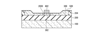
続いて、ゲート電極部602をマスクとして、トランジスタ形成領域1700にイオンインプランテーションによって不純物を注入することにより、不純物拡散層300を形成する。さらに、不純物拡散層300のゲート領域302の周囲に、上述のイオンインプランテーションよりは不純物濃度が薄くなるように所望の不純物を注入し、不純物拡散層300中にLDD(Lightly Doped Drain)層2000を形成する。このようにして、図19に示される構造を得ることができる。なお、LDD層2000を形成した後に、上述のイオンインプランテーションを行ってもよい。
さらに、ゲート電極部602をマスクとして、エッチングを行うことにより、ゲート絶縁膜500に対してパターニングを行う。その後、露出した不純物拡散層300の上面であって、ゲート電極部602の両側のゲート電極部602から離隔した位置にシリサイド膜702を形成してもよい。なお、本実施形態においては、上述のシリサイド膜702の形成方法は、特に限定されるものではなく、既知の各種の形成方法を用いることができる。
続いて、ゲート電極部602をマスクとして、トランジスタ形成領域1700にイオンインプランテーションによって不純物を注入することにより、不純物拡散層300を形成する。さらに、不純物拡散層300のゲート領域302の周囲に、上述のイオンインプランテーションよりは不純物濃度が薄くなるように所望の不純物を注入し、不純物拡散層300中にLDD(Lightly Doped Drain)層2000を形成する。このようにして、図19に示される構造を得ることができる。なお、LDD層2000を形成した後に、上述のイオンインプランテーションを行ってもよい。
さらに、ゲート電極部602をマスクとして、エッチングを行うことにより、ゲート絶縁膜500に対してパターニングを行う。その後、露出した不純物拡散層300の上面であって、ゲート電極部602の両側のゲート電極部602から離隔した位置にシリサイド膜702を形成してもよい。なお、本実施形態においては、上述のシリサイド膜702の形成方法は、特に限定されるものではなく、既知の各種の形成方法を用いることができる。
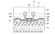
続いて、不純物拡散層300、STI204、及びゲート電極部602上に、順次、シリコン酸化膜202、シリコン窒化膜400及びシリコン酸化膜802を形成する。そして、シリコン酸化膜802から、シリコン窒化膜400及びシリコン酸化膜202を貫きシリサイド膜702まで到達するソースコンタクトビア700a及びドレインコンタクトビア700bを形成する。この際、本実施形態においては、広い薄膜部300a上に、ソースコンタクトビア700aとドレインコンタクトビア700bとを所定の距離だけ離隔して設けることができる。従って、ソースコンタクトビア700aとドレインコンタクトビア700bとを高精度でパターニングすることを避けることができることから、製造歩留まりの低下を避けることができる。また、ソースコンタクトビア700a及びドレインコンタクトビア700bを互いに所定の距離だけ離隔して設けることができることから、特に、複数のゲートを持つトランジスタにおいて、トランジスタのレイアウトサイズの増加を抑え、ひいては製造コストの増加を抑えることができる。
さらに、ソースコンタクトビア700a上に、ソース電極800aを形成し、ドレインコンタクトビア700b上に、ドレイン電極800bを形成する。この際、上述のシリコン酸化膜202、シリコン窒化膜400、シリコン酸化膜802、ソースコンタクトビア700a、ドレインコンタクトビア700b、ソース電極800a及びドレイン電極800bの形成方法は、特に限定されるものではなく、半導体装置10の製造方法において一般的に用いられている形成方法を用いることができる。さらに、これらソース電極800a及びドレイン電極800bの上に、更なる金属膜を形成してもよい。このようにして、図1から図4に示される本開示の実施形態に係る半導体装置10を得ることができる。
さらに、ソースコンタクトビア700a上に、ソース電極800aを形成し、ドレインコンタクトビア700b上に、ドレイン電極800bを形成する。この際、上述のシリコン酸化膜202、シリコン窒化膜400、シリコン酸化膜802、ソースコンタクトビア700a、ドレインコンタクトビア700b、ソース電極800a及びドレイン電極800bの形成方法は、特に限定されるものではなく、半導体装置10の製造方法において一般的に用いられている形成方法を用いることができる。さらに、これらソース電極800a及びドレイン電極800bの上に、更なる金属膜を形成してもよい。このようにして、図1から図4に示される本開示の実施形態に係る半導体装置10を得ることができる。
<実施形態の比較例>
図21は、比較例とする半導体装置10の平面を示す。なお、図21において、上記図1と同一部分には、同一符号を付して詳細な説明を省略する。
比較例にあって、不純物拡散層300の端部301のみの膜厚を厚くすることで、低寄生容量と高信頼性、低コストを実現している。
しかしながら、トランジスタ12のサイズが大きくなると、STI形成時のCMP工程において、ゲート電極配線引き出し部604の不純物拡散層300に物理的ダメージ(微小クラックなど)を受け易くなり、その後の熱酸化工程でゲート絶縁膜500の膜質が劣化、電界に対する耐圧劣化で、ゲートリーク不良を発生させる問題があった。
図21は、比較例とする半導体装置10の平面を示す。なお、図21において、上記図1と同一部分には、同一符号を付して詳細な説明を省略する。
比較例にあって、不純物拡散層300の端部301のみの膜厚を厚くすることで、低寄生容量と高信頼性、低コストを実現している。
しかしながら、トランジスタ12のサイズが大きくなると、STI形成時のCMP工程において、ゲート電極配線引き出し部604の不純物拡散層300に物理的ダメージ(微小クラックなど)を受け易くなり、その後の熱酸化工程でゲート絶縁膜500の膜質が劣化、電界に対する耐圧劣化で、ゲートリーク不良を発生させる問題があった。
<第1の実施形態の解決手段>
そこで、本第1の実施形態では、図1(a)に示すように、ゲート電極配線部600と、不純物拡散層300の端部301とが交差する部分の近傍に、半導体基板のシリコン層320からなる不純物拡散層300の側面から外側へ突出させた2つの突起部350a,350bを形成している。
2つの突起部350a,350bは、ゲート電極配線部600の延伸方向と平行方向に0.4μm以上、垂直方向に0.7μm以上の長さである。なお、好ましくは、平行方向に1μm以上、垂直方向に1μm以上である。
また、2つの突起部350a,350bは、ゲート電極配線引き出し部604との距離が、14nm以上、200nm以下である。
そこで、本第1の実施形態では、図1(a)に示すように、ゲート電極配線部600と、不純物拡散層300の端部301とが交差する部分の近傍に、半導体基板のシリコン層320からなる不純物拡散層300の側面から外側へ突出させた2つの突起部350a,350bを形成している。
2つの突起部350a,350bは、ゲート電極配線部600の延伸方向と平行方向に0.4μm以上、垂直方向に0.7μm以上の長さである。なお、好ましくは、平行方向に1μm以上、垂直方向に1μm以上である。
また、2つの突起部350a,350bは、ゲート電極配線引き出し部604との距離が、14nm以上、200nm以下である。
<第1の実施形態による作用効果>
以上のように上記第1の実施形態によれば、ゲート電極配線引き出し部604を挟み込む2つの突起部350a,350bを形成することにより、突起部350a,350bを形成した分だけ不純物拡散層300の端部301の面積及び膜厚を確保することで、不純物拡散層300の端部301とゲート電極配線部600とが交差する領域をCMPダメージから保護し、ゲートリークを防止するようにしたので、高信頼性と高歩留の確保で、製造コストの低コスト化を実現できる。
以上のように上記第1の実施形態によれば、ゲート電極配線引き出し部604を挟み込む2つの突起部350a,350bを形成することにより、突起部350a,350bを形成した分だけ不純物拡散層300の端部301の面積及び膜厚を確保することで、不純物拡散層300の端部301とゲート電極配線部600とが交差する領域をCMPダメージから保護し、ゲートリークを防止するようにしたので、高信頼性と高歩留の確保で、製造コストの低コスト化を実現できる。
また、第1の実施形態によれば、突起部350a,350bとゲート電極配線引き出し部604との距離を、14nm以上、200nm以下としたので、突起部350a,350bにゲート電極配線引き出し部604の材質が残らず、不要なゲート寄生容量の増加の防止と、発塵の抑制で高信頼性と高歩留の確保で、製造コストの増加を抑制できる。
<第1の実施形態の第1の変形例>
図22は、本開示の第1の実施形態の第1の変形例として、半導体装置10Aの平面を示す。図22において、上記図1(a)と同一部分には、同一符号を付して詳細な説明を省略する。
図22は、本開示の第1の実施形態の第1の変形例として、半導体装置10Aの平面を示す。図22において、上記図1(a)と同一部分には、同一符号を付して詳細な説明を省略する。
トランジスタ12Aは、ゲート電極部602と、ゲート電極配線部600の引き出し部であるゲート電極配線引き出し部604とを形成している。また、トランジスタ12Aは、ゲート電極配線部600と、トランジスタ12Aの端部301とが交差する部分の近傍に、半導体基板のシリコン層320からなる不純物拡散層300の側面から外側へ突出させた1つの突起部350aを形成している。第1の変形例では、2本以上のゲート電極配線引き出し部604を平行に配置している場合に、互いに対向するゲート電極配線引き出し部604の端部と反対側、つまり外側に突起部350aを形成するようにしている。
このような第1の変形例であっても、上記第1の実施形態と同様の作用効果が得られる。
このような第1の変形例であっても、上記第1の実施形態と同様の作用効果が得られる。
<第1の実施形態の第2の変形例>
図23は、本開示の第1の実施形態の第2の変形例として、半導体装置10Bの平面を示す。図23において、上記図1(a)と同一部分には、同一符号を付して詳細な説明を省略する。
図23は、本開示の第1の実施形態の第2の変形例として、半導体装置10Bの平面を示す。図23において、上記図1(a)と同一部分には、同一符号を付して詳細な説明を省略する。
図23(a)において、トランジスタ12Bは、ゲート電極配線部600と、トランジスタ12Bの端部301とが交差する部分の近傍に、半導体基板のシリコン層320からなる不純物拡散層300の側面から外側へ突出させた2つの突起部351a,351bを形成している。2つの突起部351a,351bは、トランジスタ12Bの上方から見て、丸形の形状である。
また、図23(b)において、2つの突起部352a,352bは、トランジスタ12Bの上方から見て、三角形である。また、図23(c)において、2つの突起部353a,353bは、図23(b)とは向きが異なる三角形である。さらに、図23(d)において、2つの突起部354a,354bは、トランジスタ12Bの上方から見て、多角形である。
このような第2の変形例であっても、上記第1の実施形態と同様の作用効果が得られる。
このような第2の変形例であっても、上記第1の実施形態と同様の作用効果が得られる。
<第2の実施形態>
図24は、本開示の第2の実施形態として、半導体装置10Cの平面を示す。図23において、上記図1(a)と同一部分には、同一符号を付して詳細な説明を省略する。図25は、図24に示した半導体装置10CのA-A´における断面図である。図25において、上記図2と同一部分には、同一符号を付して詳細な説明を省略する。
図24は、本開示の第2の実施形態として、半導体装置10Cの平面を示す。図23において、上記図1(a)と同一部分には、同一符号を付して詳細な説明を省略する。図25は、図24に示した半導体装置10CのA-A´における断面図である。図25において、上記図2と同一部分には、同一符号を付して詳細な説明を省略する。
図24に示されるように、半導体装置10C及びトランジスタ12Cは、シリコン支持基板100の上方から見て、はしご形状の複数のゲート電極部602と、2本のゲート電極配線部600Aとを有している。詳細には、複数のゲート電極部602は、図24中を左右方向に沿って並んでいる。2本のゲート電極配線部600Aは、複数のゲート電極部602を図24中の上下方向に沿って挟み込み、複数のゲート電極部602を互いに接続する。さらに、各ゲート電極部602を図24中の左右方向から挟み込むように、ソース電極800a及びドレイン電極800bが設けられている。
また、半導体装置10C及びトランジスタ12Cは、ゲート電極配線部600Aと、トランジスタ12Cの端部301とが交差する部分の近傍に、半導体基板のシリコン層320からなる不純物拡散層300の側面から外側へ突出させた2つの突起部350a,350bを形成している。また、ゲート電極配線部600Aは、トランジスタ12Cの端部301を超えてゲート電極配線引き出し部604を形成している。
また、本第2の実施形態においても、図25に示すように、不純物拡散層300は、上述の第1の実施形態と同様に、中央部に位置する薄膜部300aと、端部301に位置する厚膜部300bとを有する。本第2の実施形態においても、ゲート領域302、ソース領域304a及びドレイン領域304bは、不純物拡散層300の薄膜部300aに設けられている。このように、複数のゲート領域302を持つ場合であっても、薄膜部300aと厚膜部300bとを有する不純物拡散層300を適用することができる。
このような第2の実施形態であっても、上記第1の実施形態と同様の作用効果が得られる。
このような第2の実施形態であっても、上記第1の実施形態と同様の作用効果が得られる。
<第3の実施形態>
図26は、本開示の第3の実施形態として、半導体装置10Dの平面を示す。図26において、上記図1(a)と同一部分には、同一符号を付して詳細な説明を省略する。また、図27は、図26に示した半導体装置10DのA-A´における断面図である。図27において、上記図2と同一部分には、同一符号を付して詳細な説明を省略する。さらに、図28は、図26に示した半導体装置10DのB-B´における断面図である。図28において、上記図4と同一部分には、同一符号を付して詳細な説明を省略する。
図26は、本開示の第3の実施形態として、半導体装置10Dの平面を示す。図26において、上記図1(a)と同一部分には、同一符号を付して詳細な説明を省略する。また、図27は、図26に示した半導体装置10DのA-A´における断面図である。図27において、上記図2と同一部分には、同一符号を付して詳細な説明を省略する。さらに、図28は、図26に示した半導体装置10DのB-B´における断面図である。図28において、上記図4と同一部分には、同一符号を付して詳細な説明を省略する。
図26に示されるように、第3の実施形態に係る半導体装置10Dは、シリコン支持基板100の上方から見て、T字型形状となるゲート電極配線部600Bとゲート電極部602Aとを有している。詳細には、ゲート電極部602Aは、図26中の上下方向に沿って延びる矩形型である。ゲート電極配線部600Bは、図26中の左右方向に沿って延びる矩形状の配線部である。また、ゲート電極部602Aを図26中の左右方向から挟み込むように、ソース電極800a、ドレイン電極800bが設けられている。
また、半導体装置10D及びトランジスタ12Dは、ゲート電極配線部600Bと、トランジスタ12Dの端部301とが交差する部分の近傍に、半導体基板のシリコン層320からなる不純物拡散層300の側面から外側へ突出させた2つの突起部350a,350bを形成している。さらに、半導体装置10D及びトランジスタ12Dは、ゲート電極部602Aと、トランジスタ12Dの端部301とが交差する部分の近傍に、半導体基板のシリコン層320からなる不純物拡散層300の側面から外側へ突出させた2つの突起部360a,360bを形成している。また、ゲート電極部602Aは、トランジスタ12Dの端部301を超えたゲート電極引き出し部605を形成している。
また、本第3の実施形態においても、図27に示すように、不純物拡散層300は、上述の第1の実施形態と同様に、中央部に位置する薄膜部300aと、端部301に位置する厚膜部300bとを有する。本第3の実施形態においても、ゲート領域302、ソース領域304a及びドレイン領域304bは、不純物拡散層300の薄膜部300aに設けられている。このように、T字型となるゲート電極配線部600B及びゲート電極部602Aを持つ場合であっても、薄膜部300aと厚膜部300bとを有する不純物拡散層300を適用することができる。
このような第3の実施形態であっても、上記第1の実施形態と同様の作用効果が得られる。
このような第3の実施形態であっても、上記第1の実施形態と同様の作用効果が得られる。
<第4の実施形態>
図29は、本開示の第4の実施形態として、半導体装置10Eの平面を示す。図29において、上記図26と同一部分には、同一符号を付して詳細な説明を省略する。また、図30は、図29に示した半導体装置10EのA-A´における断面図である。図30において、上記図2と同一部分には、同一符号を付して詳細な説明を省略する。さらに、図31は、図29に示した半導体装置10EのB-B´における断面図である。図31において、上記図4と同一部分には、同一符号を付して詳細な説明を省略する。
図29は、本開示の第4の実施形態として、半導体装置10Eの平面を示す。図29において、上記図26と同一部分には、同一符号を付して詳細な説明を省略する。また、図30は、図29に示した半導体装置10EのA-A´における断面図である。図30において、上記図2と同一部分には、同一符号を付して詳細な説明を省略する。さらに、図31は、図29に示した半導体装置10EのB-B´における断面図である。図31において、上記図4と同一部分には、同一符号を付して詳細な説明を省略する。
図29に示されるように、第4の実施形態に係る半導体装置10Eは、シリコン支持基板100の上方から見て、I字型形状のゲート電極部602Bを有している。詳細には、ゲート電極部602Bは、図29中の上下方向に沿って延びる矩形型の形状を持つ。さらに、ゲート電極部602Bを図29中の左右方向から挟み込むように、ソース電極800a、ドレイン電極800bが設けられている。
また、半導体装置10E及びトランジスタ12Eは、ゲート電極部602Bと、トランジスタ12Eの端部301とが交差する部分の近傍に、半導体基板のシリコン層320からなる不純物拡散層300の側面から外側へ突出させた2つの突起部360a,360bを形成している。また、ゲート電極部602Bは、トランジスタ12Eの端部301を超えてゲート電極引き出し部605を形成している。
また、本第4の実施形態においては、不純物拡散層300は、上述の第1の実施形態と同様に、中央部に位置する薄膜部300aと、端部301に位置する厚膜部300bとを有する。本第4の実施形態においても、ゲート領域302、ソース領域304a及びドレイン領域304bは、不純物拡散層300の薄膜部300aに設けられている。このように、I字型のゲート電極部602Bを持つ場合であっても、薄膜部300aと厚膜部300bとを有する不純物拡散層300を適用することができる。
このような第4の実施形態であっても、上記第1の実施形態と同様の作用効果が得られる。
このような第4の実施形態であっても、上記第1の実施形態と同様の作用効果が得られる。
<その他の実施形態>
上記のように、本技術は第1から第4の実施形態及び第1の実施形態の第1及び第2の変形例によって記載したが、この開示の一部をなす論述及び図面は本技術を限定するものであると理解すべきではない。上記の第1から第3の実施形態が開示する技術内容の趣旨を理解すれば、当業者には様々な代替実施形態、実施例及び運用技術が本技術に含まれ得ることが明らかとなろう。また、第1から第4の実施形態及び第1の実施形態の第1及び第2の変形例がそれぞれ開示する構成を、矛盾の生じない範囲で適宜組み合わせることができる。例えば、複数の異なる実施形態がそれぞれ開示する構成を組み合わせてもよく、同一の実施形態の複数の異なる変形例がそれぞれ開示する構成を組み合わせてもよい。
上記のように、本技術は第1から第4の実施形態及び第1の実施形態の第1及び第2の変形例によって記載したが、この開示の一部をなす論述及び図面は本技術を限定するものであると理解すべきではない。上記の第1から第3の実施形態が開示する技術内容の趣旨を理解すれば、当業者には様々な代替実施形態、実施例及び運用技術が本技術に含まれ得ることが明らかとなろう。また、第1から第4の実施形態及び第1の実施形態の第1及び第2の変形例がそれぞれ開示する構成を、矛盾の生じない範囲で適宜組み合わせることができる。例えば、複数の異なる実施形態がそれぞれ開示する構成を組み合わせてもよく、同一の実施形態の複数の異なる変形例がそれぞれ開示する構成を組み合わせてもよい。
なお、本開示は以下のような構成も取ることができる。
(1)
埋込絶縁膜と、当該埋込絶縁膜上に設けられ、半導体素子が形成される半導体層とを有する基板と、
当該半導体層上に設けられ、前記基板を上方から見た場合に、前記半導体層の中央部から前記半導体層の端部に至り延伸した配線を有するゲート電極と、
前記半導体層上に設けられるソースコンタクトビア及びドレインコンタクトビアと、
前記半導体層の端部と前記ゲート電極の配線とが交差する領域の近傍に、前記半導体層と同一の材料で形成され前記半導体層の側面から外側へ突出する突起部と、
を備え、
前記半導体層の端部は、少なくとも一部に前記半導体層のゲート電極直下の膜厚に比べて厚い厚膜領域を有し、
前記ソースコンタクトビア及び前記ドレインコンタクトビアは、当該厚膜領域以外の領域に設けられる、
半導体装置。
(2)
前記配線は、前記半導体層の端部から外側へ延伸した引き出し部を有し、
前記突起部は、前記ゲート電極の引き出し部を挟み込むように2つ以上設けられる
前記(1)に記載の半導体装置。
(3)
前記配線は、前記半導体層の端部から外側へ延伸した引き出し部を有し、
前記ゲート電極の引き出し部は、平行に複数配置され、
前記突起部は、前記ゲート電極の引き出し部同士が対向する端部と反対側の端部に設けられる
前記(1)に記載の半導体装置。
(4)
前記半導体素子を分離する素子分離部をさらに備える
前記(1)から(3)のいずれか1に記載の半導体装置。
(5)
前記半導体層の前記端部は、前記半導体層の前記中央部の膜厚に対して2倍から10倍の膜厚を有する、
前記(1)から(3)のいずれか1に記載の半導体装置。
(6)
前記半導体層の前記端部の膜厚は、140nm~200nmであり、
前記半導体層の前記中央部の膜厚は、20nm~70nmである、
前記(5)に記載の半導体装置。
(7)
前記突起部は、前記ゲート電極の配線の延伸方向と平行方向に0.4μm以上、垂直方向に0.7μm以上、または前記平行方向に1μm以上、前記垂直方向に1μm以上である、
前記(1)から(3)のいずれか1に記載の半導体装置。
(8)
前記突起部と前記ゲート電極の引き出し部との距離は、14nm以上、200nm以下である、
前記(2)または(3)のいずれか1に記載の半導体装置。
(9)
前記突起部は、前記基板の上方から見て、四角形、丸形、三角形、多角形の少なくとも1つの形状を有する、
前記(1)から(3)のいずれか1に記載の半導体装置。
(10)
前記ゲート電極は、前記基板の上方から見て、H字型、T字型、I字型、はしご型のいずれかの形状を有する、
前記(1)から(3)のいずれか1に記載の半導体装置。
(11)
埋込絶縁膜と、当該埋込絶縁膜上に設けられ、半導体素子が形成される半導体層とを有する基板を上方から見た場合に、前記半導体層の中央部から前記半導体層の端部に至り延伸した配線を有するゲート電極を、前記半導体層に形成することと、
前記半導体層の端部と前記ゲート電極の配線とが交差する領域の近傍に、前記半導体層の側面から外側へ突出する突起部を前記半導体層と同一の材料で形成することと、
前記半導体層の端部の膜厚を、前記半導体層のゲート電極直下の膜厚に比べて厚くすることと、
を含む、半導体装置の製造方法。
(1)
埋込絶縁膜と、当該埋込絶縁膜上に設けられ、半導体素子が形成される半導体層とを有する基板と、
当該半導体層上に設けられ、前記基板を上方から見た場合に、前記半導体層の中央部から前記半導体層の端部に至り延伸した配線を有するゲート電極と、
前記半導体層上に設けられるソースコンタクトビア及びドレインコンタクトビアと、
前記半導体層の端部と前記ゲート電極の配線とが交差する領域の近傍に、前記半導体層と同一の材料で形成され前記半導体層の側面から外側へ突出する突起部と、
を備え、
前記半導体層の端部は、少なくとも一部に前記半導体層のゲート電極直下の膜厚に比べて厚い厚膜領域を有し、
前記ソースコンタクトビア及び前記ドレインコンタクトビアは、当該厚膜領域以外の領域に設けられる、
半導体装置。
(2)
前記配線は、前記半導体層の端部から外側へ延伸した引き出し部を有し、
前記突起部は、前記ゲート電極の引き出し部を挟み込むように2つ以上設けられる
前記(1)に記載の半導体装置。
(3)
前記配線は、前記半導体層の端部から外側へ延伸した引き出し部を有し、
前記ゲート電極の引き出し部は、平行に複数配置され、
前記突起部は、前記ゲート電極の引き出し部同士が対向する端部と反対側の端部に設けられる
前記(1)に記載の半導体装置。
(4)
前記半導体素子を分離する素子分離部をさらに備える
前記(1)から(3)のいずれか1に記載の半導体装置。
(5)
前記半導体層の前記端部は、前記半導体層の前記中央部の膜厚に対して2倍から10倍の膜厚を有する、
前記(1)から(3)のいずれか1に記載の半導体装置。
(6)
前記半導体層の前記端部の膜厚は、140nm~200nmであり、
前記半導体層の前記中央部の膜厚は、20nm~70nmである、
前記(5)に記載の半導体装置。
(7)
前記突起部は、前記ゲート電極の配線の延伸方向と平行方向に0.4μm以上、垂直方向に0.7μm以上、または前記平行方向に1μm以上、前記垂直方向に1μm以上である、
前記(1)から(3)のいずれか1に記載の半導体装置。
(8)
前記突起部と前記ゲート電極の引き出し部との距離は、14nm以上、200nm以下である、
前記(2)または(3)のいずれか1に記載の半導体装置。
(9)
前記突起部は、前記基板の上方から見て、四角形、丸形、三角形、多角形の少なくとも1つの形状を有する、
前記(1)から(3)のいずれか1に記載の半導体装置。
(10)
前記ゲート電極は、前記基板の上方から見て、H字型、T字型、I字型、はしご型のいずれかの形状を有する、
前記(1)から(3)のいずれか1に記載の半導体装置。
(11)
埋込絶縁膜と、当該埋込絶縁膜上に設けられ、半導体素子が形成される半導体層とを有する基板を上方から見た場合に、前記半導体層の中央部から前記半導体層の端部に至り延伸した配線を有するゲート電極を、前記半導体層に形成することと、
前記半導体層の端部と前記ゲート電極の配線とが交差する領域の近傍に、前記半導体層の側面から外側へ突出する突起部を前記半導体層と同一の材料で形成することと、
前記半導体層の端部の膜厚を、前記半導体層のゲート電極直下の膜厚に比べて厚くすることと、
を含む、半導体装置の製造方法。
10,10A,10B,10C,10D,10E…半導体装置、12,12A,12B,12C,12D,12E…トランジスタ、100…シリコン支持基板、200…埋込絶縁膜、202…シリコン酸化膜、204…STI(分離絶縁膜)、400…シリコン窒化膜、802…シリコン酸化膜、300…不純物拡散層(半導体層)、300a…薄膜部、300b…厚膜部、301…トランジスタの端部、302…ゲート領域、304a…ソース領域、304b…ドレイン領域、320…シリコン層、320a…中央部、320b…端部、350a,350b,351a,351b,352a,352b,353a,353b,354a,354b,360a,360b…突起部、500…ゲート絶縁膜、600,600A,600B…ゲート電極配線部、602,602A,602B…ゲート電極部、604…ゲート電極配線引き出し部、605…ゲート電極引き出し部、700a…ソースコンタクトビア、700b…ドレインコンタクトビア、700c…ボディコンタクトビア、702…シリサイド膜、800a…ソース電極、800b…ドレイン電極、800c…ボディコンタクト電極、900…シリコン酸化膜、902…シリコン窒化膜、904…レジストパターン、906…開口部、907…シリコン酸化膜、908…シリコン薄膜部、1000…シリコン酸化膜、1100…シリコン窒化膜、1200…レジスト膜、1300…レジストパターン、1600…開口部、1400…シリコン酸化膜、1500…レジスト膜、1700…トランジスタ形成領域、350a’,350b’…突起部を有するレジストパターン、2000…LDD層、305a…ソースN+領域、305b…ドレインN+領域
Claims (11)
- 埋込絶縁膜と、当該埋込絶縁膜上に設けられ、半導体素子が形成される半導体層とを有する基板と、
当該半導体層上に設けられ、前記基板を上方から見た場合に、前記半導体層の中央部から前記半導体層の端部に至り延伸した配線を有するゲート電極と、
前記半導体層上に設けられるソースコンタクトビア及びドレインコンタクトビアと、
前記半導体層の端部と前記ゲート電極の配線とが交差する領域の近傍に、前記半導体層と同一の材料で形成され前記半導体層の側面から外側へ突出する突起部と、
を備え、
前記半導体層の端部は、少なくとも一部に前記半導体層のゲート電極直下の膜厚に比べて厚い厚膜領域を有し、
前記ソースコンタクトビア及び前記ドレインコンタクトビアは、当該厚膜領域以外の領域に設けられる、
半導体装置。 - 前記配線は、前記半導体層の端部から外側へ延伸した引き出し部を有し、
前記突起部は、前記ゲート電極の引き出し部を挟み込むように2つ以上設けられる
請求項1に記載の半導体装置。 - 前記配線は、前記半導体層の端部から外側へ延伸した引き出し部を有し、
前記ゲート電極の引き出し部は、平行に複数配置され、
前記突起部は、前記ゲート電極の引き出し部同士が対向する端部と反対側の端部に設けられる
請求項1に記載の半導体装置。 - 前記半導体素子を分離する素子分離部をさらに備える
請求項1から請求項3のいずれか1項に記載の半導体装置。 - 前記半導体層の前記端部は、前記半導体層の前記中央部の膜厚に対して2倍から10倍の膜厚を有する、
請求項1から請求項3のいずれか1項に記載の半導体装置。 - 前記半導体層の前記端部の膜厚は、140nm~200nmであり、
前記半導体層の前記中央部の膜厚は、20nm~70nmである、
請求項5に記載の半導体装置。 - 前記突起部は、前記ゲート電極の配線の延伸方向と平行方向に0.4μm以上、垂直方向に0.7μm以上、または前記平行方向に1μm以上、前記垂直方向に1μm以上である、
請求項1から請求項3のいずれか1項に記載の半導体装置。 - 前記突起部と前記ゲート電極の引き出し部との距離は、14nm以上、200nm以下である、
請求項2または請求項3のいずれか1項に記載の半導体装置。 - 前記突起部は、前記基板の上方から見て、四角形、丸形、三角形、多角形の少なくとも1つの形状を有する、
請求項1から請求項3のいずれか1項に記載の半導体装置。 - 前記ゲート電極は、前記基板の上方から見て、H字型、T字型、I字型、はしご型のいずれかの形状を有する、
請求項1から請求項3のいずれか1項に記載の半導体装置。 - 埋込絶縁膜と、当該埋込絶縁膜上に設けられ、半導体素子が形成される半導体層とを有する基板を上方から見た場合に、前記半導体層の中央部から前記半導体層の端部に至り延伸した配線を有するゲート電極を、前記半導体層に形成することと、
前記半導体層の端部と前記ゲート電極の配線とが交差する領域の近傍に、前記半導体層の側面から外側へ突出する突起部を前記半導体層と同一の材料で形成することと、
前記半導体層の端部の膜厚を、前記半導体層のゲート電極直下の膜厚に比べて厚くすることと、
を含む、半導体装置の製造方法。
Priority Applications (2)
| Application Number | Priority Date | Filing Date | Title |
|---|---|---|---|
| US18/003,970 US12408376B2 (en) | 2020-07-13 | 2021-05-19 | Semiconductor apparatus and manufacturing method for semiconductor apparatus |
| CN202180048312.8A CN115836395A (zh) | 2020-07-13 | 2021-05-19 | 半导体装置及半导体装置的制造方法 |
Applications Claiming Priority (2)
| Application Number | Priority Date | Filing Date | Title |
|---|---|---|---|
| JP2020119898A JP2022016910A (ja) | 2020-07-13 | 2020-07-13 | 半導体装置及び半導体装置の製造方法 |
| JP2020-119898 | 2020-07-13 |
Publications (1)
| Publication Number | Publication Date |
|---|---|
| WO2022014152A1 true WO2022014152A1 (ja) | 2022-01-20 |
Family
ID=79554746
Family Applications (1)
| Application Number | Title | Priority Date | Filing Date |
|---|---|---|---|
| PCT/JP2021/019040 Ceased WO2022014152A1 (ja) | 2020-07-13 | 2021-05-19 | 半導体装置及び半導体装置の製造方法 |
Country Status (5)
| Country | Link |
|---|---|
| US (1) | US12408376B2 (ja) |
| JP (1) | JP2022016910A (ja) |
| CN (1) | CN115836395A (ja) |
| TW (1) | TWI900598B (ja) |
| WO (1) | WO2022014152A1 (ja) |
Citations (5)
| Publication number | Priority date | Publication date | Assignee | Title |
|---|---|---|---|---|
| JPH01204473A (ja) * | 1988-02-10 | 1989-08-17 | Hitachi Ltd | 薄膜トランジスタ |
| JP2000216391A (ja) * | 1999-01-25 | 2000-08-04 | Sony Corp | Soi型半導体装置の製造方法 |
| JP2007059747A (ja) * | 2005-08-26 | 2007-03-08 | Seiko Epson Corp | 半導体基板の製造方法及び半導体装置の製造方法、フォトマスク |
| JP2009267027A (ja) * | 2008-04-24 | 2009-11-12 | Seiko Epson Corp | 半導体装置及びその製造方法 |
| JP2018148123A (ja) * | 2017-03-08 | 2018-09-20 | ソニーセミコンダクタソリューションズ株式会社 | 半導体装置及び半導体装置の製造方法 |
Family Cites Families (3)
| Publication number | Priority date | Publication date | Assignee | Title |
|---|---|---|---|---|
| CN1577796A (zh) | 2003-07-10 | 2005-02-09 | 精工爱普生株式会社 | 电子器件的制造方法和半导体器件的制造方法 |
| JP4004448B2 (ja) | 2003-09-24 | 2007-11-07 | 富士通株式会社 | 半導体装置およびその製造方法 |
| JP7153559B2 (ja) * | 2017-07-14 | 2022-10-14 | ヌヴォトンテクノロジージャパン株式会社 | 半導体装置 |
-
2020
- 2020-07-13 JP JP2020119898A patent/JP2022016910A/ja active Pending
-
2021
- 2021-05-19 WO PCT/JP2021/019040 patent/WO2022014152A1/ja not_active Ceased
- 2021-05-19 US US18/003,970 patent/US12408376B2/en active Active
- 2021-05-19 CN CN202180048312.8A patent/CN115836395A/zh active Pending
- 2021-06-30 TW TW110124005A patent/TWI900598B/zh active
Patent Citations (5)
| Publication number | Priority date | Publication date | Assignee | Title |
|---|---|---|---|---|
| JPH01204473A (ja) * | 1988-02-10 | 1989-08-17 | Hitachi Ltd | 薄膜トランジスタ |
| JP2000216391A (ja) * | 1999-01-25 | 2000-08-04 | Sony Corp | Soi型半導体装置の製造方法 |
| JP2007059747A (ja) * | 2005-08-26 | 2007-03-08 | Seiko Epson Corp | 半導体基板の製造方法及び半導体装置の製造方法、フォトマスク |
| JP2009267027A (ja) * | 2008-04-24 | 2009-11-12 | Seiko Epson Corp | 半導体装置及びその製造方法 |
| JP2018148123A (ja) * | 2017-03-08 | 2018-09-20 | ソニーセミコンダクタソリューションズ株式会社 | 半導体装置及び半導体装置の製造方法 |
Also Published As
| Publication number | Publication date |
|---|---|
| JP2022016910A (ja) | 2022-01-25 |
| TW202209684A (zh) | 2022-03-01 |
| CN115836395A (zh) | 2023-03-21 |
| US20230261065A1 (en) | 2023-08-17 |
| TWI900598B (zh) | 2025-10-11 |
| US12408376B2 (en) | 2025-09-02 |
Similar Documents
| Publication | Publication Date | Title |
|---|---|---|
| US7754546B2 (en) | Semiconductor device manufacturing method and semiconductor device using the same | |
| US7705401B2 (en) | Semiconductor device including a fin-channel recess-gate MISFET | |
| US7638376B2 (en) | Method for forming SOI device | |
| US6395598B1 (en) | Semiconductor device and method for fabricating the same | |
| US7262109B2 (en) | Integrated circuit having a transistor level top side wafer contact and a method of manufacture therefor | |
| JP2013183133A (ja) | 半導体装置の製造方法 | |
| CN110383491B (zh) | 半导体装置及制造半导体装置的方法 | |
| CN114765171B (zh) | 半导体结构及其制作方法 | |
| KR20010093767A (ko) | 반도체 장치 및 그 제조 방법 | |
| JP2022016910A (ja) | 半導体装置及び半導体装置の製造方法 | |
| KR100546332B1 (ko) | 바이폴라 접합 트랜지스터 및 그 제조 방법 | |
| US7179713B2 (en) | Method of fabricating a fin transistor | |
| US7592208B2 (en) | Method for manufacturing semiconductor substrate and method for manufacturing semiconductor apparatus and photomask | |
| KR102920560B1 (ko) | 반도체 구조물 | |
| US20250081509A1 (en) | Gate dielectric features in high-voltage ic devices and methods of forming the same | |
| TWI891427B (zh) | 具有高壓電晶體、中壓電晶體和低壓電晶體的結構及其製作方法 | |
| KR101416318B1 (ko) | 소자 분리 공정을 포함하는 반도체 장치의 제조방법 | |
| US20240395883A1 (en) | Semiconductor structure with flush shallow trench isolation and gate oxide and method of manufacturing the same | |
| US10651183B1 (en) | Manufacturing method of semiconductor device | |
| TWI701789B (zh) | 半導體結構及其製造方法 | |
| CN120857599A (zh) | 半导体结构的制备方法、半导体结构、器件及电子设备 | |
| JP3657247B2 (ja) | 半導体装置およびその製造方法 | |
| CN121398085A (zh) | 晶体管结构及其制造方法 | |
| KR100473189B1 (ko) | 반도체소자 제조방법 | |
| CN121843154A (zh) | 半导体结构及其制造方法 |
Legal Events
| Date | Code | Title | Description |
|---|---|---|---|
| 121 | Ep: the epo has been informed by wipo that ep was designated in this application |
Ref document number: 21841951 Country of ref document: EP Kind code of ref document: A1 |
|
| NENP | Non-entry into the national phase |
Ref country code: DE |
|
| 122 | Ep: pct application non-entry in european phase |
Ref document number: 21841951 Country of ref document: EP Kind code of ref document: A1 |
|
| WWG | Wipo information: grant in national office |
Ref document number: 18003970 Country of ref document: US |