WO2022013910A1 - 発光素子およびその製造方法 - Google Patents
発光素子およびその製造方法 Download PDFInfo
- Publication number
- WO2022013910A1 WO2022013910A1 PCT/JP2020/027223 JP2020027223W WO2022013910A1 WO 2022013910 A1 WO2022013910 A1 WO 2022013910A1 JP 2020027223 W JP2020027223 W JP 2020027223W WO 2022013910 A1 WO2022013910 A1 WO 2022013910A1
- Authority
- WO
- WIPO (PCT)
- Prior art keywords
- light emitting
- semiconductor layer
- layer
- emitting device
- nitride semiconductor
- Prior art date
- Legal status (The legal status is an assumption and is not a legal conclusion. Google has not performed a legal analysis and makes no representation as to the accuracy of the status listed.)
- Ceased
Links
Images




Classifications
-
- H—ELECTRICITY
- H10—SEMICONDUCTOR DEVICES; ELECTRIC SOLID-STATE DEVICES NOT OTHERWISE PROVIDED FOR
- H10H—INORGANIC LIGHT-EMITTING SEMICONDUCTOR DEVICES HAVING POTENTIAL BARRIERS
- H10H20/00—Individual inorganic light-emitting semiconductor devices having potential barriers, e.g. light-emitting diodes [LED]
- H10H20/80—Constructional details
- H10H20/81—Bodies
- H10H20/822—Materials of the light-emitting regions
- H10H20/824—Materials of the light-emitting regions comprising only Group III-V materials, e.g. GaP
- H10H20/825—Materials of the light-emitting regions comprising only Group III-V materials, e.g. GaP containing nitrogen, e.g. GaN
-
- H—ELECTRICITY
- H10—SEMICONDUCTOR DEVICES; ELECTRIC SOLID-STATE DEVICES NOT OTHERWISE PROVIDED FOR
- H10H—INORGANIC LIGHT-EMITTING SEMICONDUCTOR DEVICES HAVING POTENTIAL BARRIERS
- H10H20/00—Individual inorganic light-emitting semiconductor devices having potential barriers, e.g. light-emitting diodes [LED]
- H10H20/01—Manufacture or treatment
- H10H20/011—Manufacture or treatment of bodies, e.g. forming semiconductor layers
- H10H20/013—Manufacture or treatment of bodies, e.g. forming semiconductor layers having light-emitting regions comprising only Group III-V materials
- H10H20/0133—Manufacture or treatment of bodies, e.g. forming semiconductor layers having light-emitting regions comprising only Group III-V materials with a substrate not being Group III-V materials
- H10H20/01335—Manufacture or treatment of bodies, e.g. forming semiconductor layers having light-emitting regions comprising only Group III-V materials with a substrate not being Group III-V materials the light-emitting regions comprising nitride materials
-
- H—ELECTRICITY
- H10—SEMICONDUCTOR DEVICES; ELECTRIC SOLID-STATE DEVICES NOT OTHERWISE PROVIDED FOR
- H10H—INORGANIC LIGHT-EMITTING SEMICONDUCTOR DEVICES HAVING POTENTIAL BARRIERS
- H10H20/00—Individual inorganic light-emitting semiconductor devices having potential barriers, e.g. light-emitting diodes [LED]
- H10H20/01—Manufacture or treatment
- H10H20/011—Manufacture or treatment of bodies, e.g. forming semiconductor layers
- H10H20/013—Manufacture or treatment of bodies, e.g. forming semiconductor layers having light-emitting regions comprising only Group III-V materials
- H10H20/0137—Manufacture or treatment of bodies, e.g. forming semiconductor layers having light-emitting regions comprising only Group III-V materials the light-emitting regions comprising nitride materials
-
- H—ELECTRICITY
- H10—SEMICONDUCTOR DEVICES; ELECTRIC SOLID-STATE DEVICES NOT OTHERWISE PROVIDED FOR
- H10H—INORGANIC LIGHT-EMITTING SEMICONDUCTOR DEVICES HAVING POTENTIAL BARRIERS
- H10H20/00—Individual inorganic light-emitting semiconductor devices having potential barriers, e.g. light-emitting diodes [LED]
- H10H20/80—Constructional details
- H10H20/81—Bodies
- H10H20/817—Bodies characterised by the crystal structures or orientations, e.g. polycrystalline, amorphous or porous
Definitions
- the present invention relates to a light emitting device composed of a layered substance and a method for manufacturing the same.
- Hexagonal boron nitride is a semiconductor material having a bandgap energy corresponding to an emission wavelength of about 215 nm, but the emission wavelength is set by a mixed crystal with Al, Ga, and In, which are group III elements other than boron. It is also possible to control.
- This light emitting device first includes a vacuum container 301, a glass plate 302 forming one surface of the vacuum container 301, and a light emitting layer 303 formed on the inner side of the vacuum container 301 of the glass plate 302. Further, this light emitting device includes a power supply 304 that applies an acceleration voltage to the light emitting layer 303, and an electron beam source 305 that irradiates the light emitting layer 303 with an electron beam 321.
- the light emitting layer 303 is composed of an undoped h-BN powder.
- the electron beam source 305 is a field emission type electron gun 311, a constant voltage circuit 312 that applies a voltage to the electron gun 311, a gate electrode 313 for electric emission of electrons from the electron gun 311, and a gate to the gate electrode 313.
- a gate power supply 314 for applying a voltage is provided.
- Electrons and holes are generated in the h-BN of the light emitting layer 303 by the high energy electron beam 321 irradiated from the electron beam source 305 to the light emitting layer 303.
- light 322 having a wavelength of 225 nm is generated from the light emitting layer 303.
- the emission wavelength derived from the free excitons of h-BN is 215 nm, but the emission having a wavelength of 225 nm is derived from bound excitons due to impurities or crystal defects, phonon replicas of free excitons, and the like.
- Kenji Watanabe et al. "Far-ultraviolet plane-emission handheld device based on hexagonal boron nitride", Nature Photonics, vol. 3, pp. 591-594, 2009.
- the light emitting intensity is improved by increasing the energy and the amount of current of the emitted electrons, but for this purpose, it is necessary to increase the size of the electron beam source. Further, since the electron beam source requires a vacuum structure and the structure is complicated, it is difficult to manufacture a small ultraviolet light emitting device.
- the device structure is to be miniaturized, it becomes difficult to increase the energy and current amount of the irradiated electrons, and high emission intensity cannot be obtained. So far, in a device size of 6.5 cm ⁇ 3.5 cm, the emission intensity has been 1 mW and the external quantum efficiency has remained at about 0.6% under the operating conditions of an acceleration voltage of 9 kV and an anode current of 100 ⁇ A.
- the present invention has been made to solve the above-mentioned problems, and an object of the present invention is to enable a small element using a layered BN or a layer of this mixed crystal to obtain high emission intensity. do.
- the light emitting device has a light emitting layer made of an i-type layered nitride semiconductor and a p-type layered nitride semiconductor or p-type arranged on one surface of the light emitting layer. It includes a first semiconductor layer made of diamond and a second semiconductor layer made of an n-type layered nitride semiconductor arranged on the other surface of the light emitting layer.
- the method for manufacturing a light emitting device is the above-mentioned method for manufacturing a light emitting element, which comprises a step of forming a light emitting layer, a step of forming a first semiconductor layer, and a second semiconductor layer.
- the layered nitride semiconductor is formed by a structural phase transition from a flash zinc ore structure to a layered structure, which comprises a step of forming.
- a high emission intensity can be obtained with a small element using a layered BN or a layer of this mixed crystal.
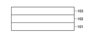
- FIG. 1A is a cross-sectional view showing a state of a light emitting element in an intermediate step for explaining a method for manufacturing a light emitting element according to an embodiment of the present invention.
- FIG. 1B is a cross-sectional view showing a state of a light emitting element in an intermediate process for explaining a method for manufacturing a light emitting element according to an embodiment of the present invention.
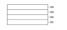
- FIG. 1C is a cross-sectional view showing a state of a light emitting element in an intermediate process for explaining a method for manufacturing a light emitting element according to an embodiment of the present invention.
- FIG. 1A is a cross-sectional view showing a state of a light emitting element in an intermediate step for explaining a method for manufacturing a light emitting element according to an embodiment of the present invention.
- FIG. 1B is a cross-sectional view showing a state of a light emitting element in an intermediate process for explaining a method for manufacturing a light emitting element according to an embodiment of the present invention.
- FIG. 1D is a cross-sectional view showing a state of a light emitting element in an intermediate process for explaining a method for manufacturing a light emitting element according to an embodiment of the present invention.
- FIG. 1E is a cross-sectional view showing a state of a light emitting element in an intermediate process for explaining a method for manufacturing a light emitting element according to an embodiment of the present invention.
- FIG. 1F is a cross-sectional view showing a state of a light emitting element in an intermediate process for explaining a method for manufacturing a light emitting element according to an embodiment of the present invention.
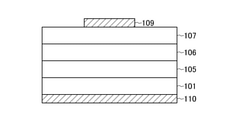
- FIG. 2 is a configuration diagram showing a configuration of a light emitting device according to an embodiment of the present invention.
- FIG. 3 is a configuration diagram showing a configuration of a light emitting device.
- FIGS. 1A to 1F a method for manufacturing a light emitting device according to an embodiment of the present invention will be described with reference to FIGS. 1A to 1F.
- the first semiconductor layer 102 is formed on the substrate 101.
- the substrate 101 is made of, for example, diamond having a high concentration of B doped into a p-type and having a (111) surface as a main surface.
- the substrate 101 can be composed of any of c-BN, 3C-SiC, 4H-SiC, 6H-SiC, and Si.
- the main surface of the substrate composed of c-BN, 3C-SiC, and Si is the (111) surface, but the main surface of the substrate composed of 4H-SiC and 6H-SiC is the (0001) surface.
- the first semiconductor layer 102 is composed of a p-type nitride semiconductor having a sphalerite structure.
- the first semiconductor layer 102 is composed of c-BN having a sphalerite structure, which is doped with Mg as an acceptor.
- the acceptor concentration of the first semiconductor layer 102 is 1 ⁇ 10 18 cm -3 , and the hole concentration at this time is 1 ⁇ 10 16 cm -3 .
- the first semiconductor layer 102 is formed to have a thickness of about 200 nm.
- the first semiconductor layer 102 can be formed by growing cubic boron nitride (c-BN) having a sphalerite structure on the substrate 101 by the well-known ion beam assist MBE method.
- the first semiconductor layer 102 grown on the substrate 101 having a main surface as a (111) plane has a main surface as a (111) plane.
- the nitride semiconductor constituting the first semiconductor layer 102 can be composed of at least one of Group III elements, Al, Ga, and In, in addition to B or B.
- the nitride semiconductor constituting the first semiconductor layer 102 can be p-type by using any one of Mg, Be, C, Zn, and Ca as an acceptor.
- the first semiconductor layer 102 can be made of p-type diamond.
- Diamond can be made p-type by doping B as an acceptor.
- the first semiconductor layer 102 can be formed by growing a p-type diamond on the substrate 101 by a known plasma CVD method.
- the acceptor concentration of B in the first semiconductor layer 102 is 1 ⁇ 10 19 cm -3
- the hole concentration is 1 ⁇ 10 16 cm -3 .
- the first semiconductor layer 102 made of p-type diamond is formed to have a thickness of 200 nm.
- an i-type light emitting layer forming layer 103 is formed on the first semiconductor layer 102.
- the light emitting layer forming layer 103 is composed of a nitride semiconductor having an undoped sphalerite structure.
- the first semiconductor layer 102 is undoped (i-type) and is composed of c-BN having a sphalerite structure.
- the light emitting layer forming layer 103 is formed by growing cubic boron nitride (c-BN) having a sphalerite structure on the first semiconductor layer 102 by the well-known ion beam assist MBE method. can.
- the light emitting layer forming layer 103 is formed to have a thickness of 1000 nm.
- the light emitting layer forming layer 103 grown on the first semiconductor layer 102 whose main surface is the (111) plane, and the main surface is the (111) plane.
- the second semiconductor layer 104 is formed on the light emitting layer forming layer 103.
- the second semiconductor layer 104 is composed of a p-type nitride semiconductor having a sphalerite structure.
- the second semiconductor layer 104 is composed of c-BN having a sphalerite structure doped with Si as a donor.
- the donor concentration of the second semiconductor layer 104 is 1 ⁇ 10 18 cm -3
- the electron concentration at this time is 1 ⁇ 10 16 cm -3 .
- the second semiconductor layer 104 is formed to have a thickness of about 200 nm.
- the second semiconductor layer 104 is formed by growing cubic boron nitride (c-BN) having a sphalerite structure on the light emitting layer forming layer 103 by the well-known ion beam assist MBE method. can.
- the second semiconductor layer 104 grown on the light emitting layer forming layer 103 having the main surface as the (111) plane has the main surface as the (111) plane.
- the nitride semiconductor constituting the second semiconductor layer 104 can be composed of at least one of Group III elements, Al, Ga, and In, in addition to B or B. Further, the nitride semiconductor constituting the second semiconductor layer 104 can be n-type by using any one of Si, O, S, and Se as a donor.
- the bandgap energy of the p-type, n-type, and i-type h-BN is 6.2 eV.
- each of the first semiconductor layer 102, the light emitting layer forming layer 103, and the second semiconductor layer 104 undergoes a structural phase transition from a succinct ore structure to a layered structure, so that, as shown in FIG. 1D, the substrate 101 Above, a first semiconductor layer 105 made of a p-type layered nitride semiconductor or a p-type diamond, a light emitting layer 106 made of an i-type layered nitride semiconductor, and an n-type were formed.
- the second semiconductor layer 107 made of a layered nitride semiconductor is in a state of being laminated in this order.
- the layer structure phase transition can be carried out by setting the temperature to 1200 ° C. or higher in an atmosphere where the pressure is 1013250 Pa or lower.
- the structural phase transition can be carried out by heat treatment under the conditions of a nitrogen atmosphere having a pressure of 79993.2 Pa, a heating temperature of 1500 ° C., and a heating time of 5 hours.
- the c-BN (nitride semiconductor) of the sphalerite structure constituting each layer undergoes a structural phase transition to h-BN, which is a layered nitride semiconductor.
- h-BN has the same acceptor concentration, hole concentration, donor concentration, and electron concentration as c-BN.
- the layered nitride semiconductor has a 2H or 3R laminated structure.
- the sphalerite structure to the layered structure can be obtained.
- the structural phase can be transferred to.
- the structural phase transition was performed by hydrogen plasma irradiation.
- Hydrogen plasma is generated by microwaves under the condition that the pressure is 333.05 Pa, and the generated hydrogen plasma is irradiated to the nitride semiconductor having a sphalerite structure under the condition of heating to 500 ° C.
- the irradiation time is 5 hours.
- the c-BN (nitride semiconductor) of the sphalerite structure constituting each layer undergoes a structural phase transition to h-BN, which is a layered nitride semiconductor.
- h-BN shows the same acceptor concentration, hole concentration, donor concentration, and electron concentration as c-BN.
- the layered nitride semiconductor has a 2H or 3R laminated structure.
- the laminated structure of the first semiconductor layer 105, the light emitting layer 106, and the second semiconductor layer 107 is processed into a mesa shape by patterning by selective etching using a mask pattern formed by a known lithography technique. As shown in FIG. 1E, a region 108 in which the surface of the substrate 101 is exposed is formed in a part of the substrate 101.
- the etching described above can be performed by, for example, a plasma etching process using chlorine (Cl 2 ) and boron trichloride gas (BCl 3) as the etching gas.
- the first electrode 109 is formed on the second semiconductor layer 107, and the second electrode 110 is formed in the region 108 of the substrate 101.
- the first electrode 109 is ohmic-connected to the second semiconductor layer 107
- the second electrode 110 is ohmic-connected to the substrate 101.
- the first electrode 109 and the second electrode 110 have a laminated structure of Ti / Pt / Au.
- the above-mentioned ohmic connection can be obtained by depositing each metal material by electron beam vapor deposition and then heat-treating it in a nitrogen atmosphere at 750 ° C. for 10 minutes.
- the light emitting device is a layered nitride semiconductor or a p-type layered nitride semiconductor arranged on one surface of a light emitting layer 106 made of an i-type layered nitride semiconductor and a light emitting layer 106. It includes a first semiconductor layer 105 made of a p-type diamond and a second semiconductor layer 107 made of an n-type layered nitride semiconductor arranged on the other surface of the light emitting layer 106.
- This light emitting device is a light emitting element that obtains light emission by injecting a current into the light emitting layer 106 with the first semiconductor layer 105 and the second semiconductor layer 107 as a current injection structure.
- the light emitting element according to the above-described embodiment is different from the conventional boron nitride light emitting element in which light emission centered at a wavelength of 225 nm derived from a phonon replica of a bound exciter or a free exciter is dominant, and is h by current injection.
- Ultraviolet light emission centered at a wavelength of 215 nm derived from the light emission recombination of the -BN free excitator was obtained from the light emitting layer 106.
- the external quantum is in a light emitting device having a plan view dimension of 3 mm ⁇ 3 mm due to the laminated structure of the first semiconductor layer 105, the light emitting layer 106, and the second semiconductor layer 107.
- the efficiency was about 10%, and when the first semiconductor layer 105 was diamond, the external quantum efficiency was about 6%.
- the element size is about 1/250 (1/250) smaller than that of the conventional boron nitride light emitting device. , 15 times higher external quantum efficiency was shown. Further, when the first semiconductor layer 105 is diamond, the element size is as small as about 1/250 (1/250), and the external quantum efficiency is about 10 times higher than that of the conventional boron nitride light emitting device.
- the mesa structure is formed on the substrate 101 to form the region 108
- the second electrode 110 is formed on the substrate 101 in the region 108
- the present invention is not limited to this.
- the second electrode 110 can be formed on the back surface of the substrate 101 as shown in FIG. 2 without forming the mesa structure as described above. In the light emitting device having this structure, high external quantum efficiency was obtained as described above.
- the acceptor concentration and the donor concentration in the nitride semiconductor are set to 1 ⁇ 10 18 cm -3 is described as an example, but in the range of 1 ⁇ 10 16 to 1 ⁇ 10 22 cm -3 , the acceptor is used.
- the acceptor concentration in the first semiconductor layer 105 is 1 ⁇ 10 17 cm -3 or more and the donor concentration in the second semiconductor layer 107 is 1 ⁇ 10 16 cm -3 or more, the outside is higher than the boron nitride light emitting device of the conventional structure. Quantum efficiency was obtained.
- the acceptor concentration in diamond is 1 ⁇ 10 19 cm -3 has been described as an example, but in the range of 1 ⁇ 10 16 to 1 ⁇ 10 22 cm -3 , the higher the acceptor concentration, the higher the external quantum. Efficiency was obtained.
- the acceptor concentration of the first semiconductor layer made of p-type diamond is 1 ⁇ 10 17 cm -3 or more and the donor concentration of the n-type second semiconductor layer is 1 ⁇ 10 16 cm -3 or more
- the conventional structure is nitrided. Higher external quantum efficiency than the boron light emitting device was obtained.
- the hole concentration and the electron concentration are set to 1 ⁇ 10 16 cm -3 is described as an example, but in the range of 1 ⁇ 10 14 to 1 ⁇ 10 20 cm -3 , the hole concentration and the hole concentration are described.
- the higher the electron concentration the higher the external quantum efficiency.
- the hole concentration of the first semiconductor layer is 1 ⁇ 10 16 cm -3 or more and the electron concentration of the second semiconductor layer is 1 ⁇ 10 15 cm -3 or more, the external structure is higher than that of the conventional boron nitride light emitting device. Quantum efficiency was obtained.
- the substrate is composed of p-type diamond doped with high concentration of B
- the substrate is p-type c-BN, p-type 3C-SiC, and p-type 4H-. Similar results were obtained when the composition was composed of SiC, p-type 6H-SiC, and p-type Si.
- the plane orientations of the main surface of each nitride semiconductor layer are (001), (110), and (113)
- the external quantum is obtained in the obtained light emitting device as compared with the case of (111). Efficiency has decreased.
- the external quantum efficiency is higher than that of (111). Has decreased. Further, when the substrate material is 4H-SiC or 6H-SiC and the plane orientations are (11-20), (1-100), (1-102), (0001), (000-1) and so on. The external quantum efficiency decreased compared to the case where.
- h-BN has been described as an example of the layered nitride semiconductor layer, but as the layered nitride semiconductor layer, a BAlGaInN mixed crystal, a BAlN mixed crystal, and a BGaN mixed crystal having a stacking period of 2H or 3R have been described.
- BINN mixed crystal, BALGaN mixed crystal, BALIN mixed crystal, BGaInN mixed crystal can be used.
- bandgap energy of the i-type light emitting layer was equal to or less than the bandgap energy of the p-type or n-type layered nitride semiconductor.
- the bandgap energy of the light emitting layer is n-type, regardless of the magnitude relationship of the bandgap energy between the light emitting layer and the first semiconductor layer. Similar results were obtained when the energy was less than the bandgap energy of the physical semiconductor.
- the emission wavelength changed according to the composition of the group III element.
- the case where the thickness of the first semiconductor layer and the second semiconductor layer is 200 nm has been described as an example, but when the thickness is 10 nm or more, the same result is obtained. Further, although the thickness of the light emitting layer was described as 1000 nm, the same result was obtained when the thickness was 2 nm or more. Further, as the growth method of c-BN, the ion beam assist MBE method has been described as an example, but the growth method of c-BN is the same even if it is a plasma CVD method or a sputtering method.
- a nitrogen atmosphere having a pressure of 79993.2 Pa and a heating temperature of 1500 ° C. has been shown, but the atmosphere is not limited to nitrogen, but an atmosphere of an inert gas such as Ar or H 2 and an atmosphere of an inert gas.
- the structural phase transition can be carried out in the same manner as described above if the heating is performed at a high temperature of 1200 ° C. or higher regardless of the pressure.
- the pressure When the pressure is higher than 980665Pa, it becomes a disordered layered irregular layered boron nitride (t-BN) or a mixed layer of t-BN and c-BN, and the nitride semiconductor layer having a stacking period of 2H or 3R becomes I could't get it. Further, when the heating temperature was less than 1200 ° C., the structural phase transition did not occur.
- the same result can be obtained not only by plasma irradiation of hydrogen plasma but also by plasma irradiation of nitrogen or argon and plasma irradiation of a mixed gas of two or more kinds of hydrogen, nitrogen and argon. rice field.
- the conditions for plasma irradiation were a pressure of 333.05 Pa and a heating temperature of 500 ° C., but the same effect was obtained if the pressure was 98066.5.5 Pa or less and the heating temperature was 100 ° C. or higher. When the pressure was higher than 98066.5.5 Pa, plasma irradiation could not be performed because the plasma did not ignite stably, and the structural phase transition did not occur when the heating temperature was less than 100 ° C.
- a light emitting layer made of a layered nitride semiconductor made of i-type and a p-type are formed by the structural phase transition from the flash zinc ore structure to the layered structure. Since the current injection structure was formed by the first semiconductor layer made of layered nitride semiconductor or p-type diamond and the second semiconductor layer made of n-type layered nitride semiconductor, the layered BN and this A small element using a mixed crystal layer can obtain high emission intensity.
Landscapes
- Led Devices (AREA)
Abstract
発光素子は、i型とされた層状の窒化物半導体からなる発光層(106)と、発光層(106)の一方の面に配置され、p型とされた層状の窒化物半導体またはp型とされたダイヤモンドからなる第1半導体層(105)と、発光層(106)の他方の面に配置され、n型とされた層状の窒化物半導体からなる第2半導体層(107)とを備える。
Description
本発明は、層状物質から構成された発光素子およびその製造方法に関する。
2Hの積層構造を持つ層状六方晶窒化ホウ素(h-BN)は、電子線照射による研究から、紫外領域で高い外部量子効率を示すことが報告されており、殺菌や高密度情報ストレージが可能な発光デバイスへの応用が期待されている。六方晶窒化ホウ素は、約215nmの発光波長に対応するバンドギャップエネルギーを有している半導体材料であるが、ホウ素以外のIII族元素であるAl、Ga、Inとの混晶によって、発光波長をコントロールすることも可能である。
ここで、h-BNを用いた深紫外線を発光する発光デバイスについて、図3を参照して説明する(非特許文献1参照)。この発光デバイスは、まず、真空容器301と、真空容器301の1つの面を構成するガラス板302と、ガラス板302の真空容器301の内部側に形成された発光層303とを備える。また、この発光デバイスは、発光層303に加速電圧を印加する電源304と、発光層303に電子線321を照射する電子線源305とを備える。
発光層303は、アンドープのh-BN粉末から構成されている。電子線源305は、電界放出型の電子銃311と、電子銃311に電圧を印加する定電圧回路312と、電子銃311から電子を電界放出させるためのゲート電極313と、ゲート電極313にゲート電圧を印加するゲート電源314とを備える。
電子線源305から発光層303に照射された高エネルギーの電子線321によって、発光層303のh-BN内に電子と正孔が生成する。この正孔と電子が再結合することによって、波長225nmを中心とした光322が、発光層303から発生する。h-BNの自由励起子に由来する発光波長は215nmであるが、波長225nmの発光は、不純物や結晶欠陥による束縛励起子や自由励起子のフォノンレプリカなどに由来している。
Kenji Watanabe et al., "Far-ultraviolet plane-emission handheld device based on hexagonal boron nitride", Nature Photonics, vol. 3, pp. 591-594, 2009.
ところで、上述した従来の発光デバイスでは、照射する電子のエネルギーおよび電流量を高くすることで発光強度は向上するが、このためには電子線源を大型化する必要がある。また、電子線源には真空構造が必要であり、構造が複雑であるため、小型の紫外発光デバイスの作製が難しい。
一方、デバイス構造を小型にしようとすると、照射する電子のエネルギーと電流量を高くすることが難しくなり、高い発光強度が得られない。これまで6.5cm×3.5cmのデバイスサイズにおいて、加速電圧9kVおよびアノード電流100μAの動作条件で、発光強度は1mWであり、外部量子効率は約0.6%に留まっていた。
本発明は、以上のような問題点を解消するためになされたものであり、層状BNやこの混晶の層を用いた小型の素子で、高い発光強度が得られるようにすることを目的とする。
本発明に係る発光素子は、i型とされた層状の窒化物半導体からなる発光層と、発光層の一方の面に配置され、p型とされた層状の窒化物半導体またはp型とされたダイヤモンドからなる第1半導体層と、発光層の他方の面に配置され、n型とされた層状の窒化物半導体からなる第2半導体層とを備える。
本発明に係る発光素子の製造方法は、上述した発光素子を製造する発光素子の製造方法であって、発光層を形成する工程と、第1半導体層を形成する工程と、第2半導体層を形成する工程とを備え、層状の窒化物半導体は、閃亜鉛鉱構造から層状構造へ構造相転移することで形成する。
以上説明したことによりように、本発明によれば、層状BNやこの混晶の層を用いた小型の素子で、高い発光強度が得られる。
以下、本発明の実施の形態に係る発光素子の製造方法について図1A~図1Fを参照して説明する。
まず、図1Aに示すように、基板101の上に、第1半導体層102を形成する。基板101は、例えば、高濃度にBがドープされてp型とされ、主表面が(111)面とされたダイヤモンドから構成されている。基板101は、c-BN、3C-SiC、4H-SiC、6H-SiC、Siのいずれかから構成することができる。なお、c-BN、3C-SiC、Siから構成する基板の主表面は(111)面となるが、4H-SiC、6H-SiCから構成する基板の主表面は(0001)面となる。
第1半導体層102は、p型とされた閃亜鉛鉱構造の窒化物半導体から構成されている。例えば、第1半導体層102は、アクセプタとしてMgがドープされた、閃亜鉛鉱構造のc-BNから構成されている。第1半導体層102のアクセプタ濃度は1×1018cm-3であり、このときの正孔濃度は1×1016cm-3である。また、第1半導体層102は、厚さ200nm程度に形成する。例えば、よく知られたイオンビームアシストMBE法により、基板101の上に、閃亜鉛鉱構造を持つ立方晶窒化ホウ素(c-BN)を成長することで、第1半導体層102が形成できる。主表面が(111)面とされた基板101の上に成長した第1半導体層102は、主表面が(111)面とされている。
なお、第1半導体層102を構成する窒化物半導体は、III族元素が、BまたはBに加えてAl、Ga、Inの少なくとも1つから構成することができる。第1半導体層102を構成する窒化物半導体は、アクセプタとして、Mg、Be、C、Zn、Caのいずれか1つを用いてp型とすることができる。
また、第1半導体層102は、p型とされたダイヤモンドから構成することができる。ダイヤモンドは、Bをアクセプタとしてドープすることで、p型とすることができる。例えば、基板101の上に、公知のプラズマCVD法により、p型とされたダイヤモンドを成長することで、第1半導体層102を形成することができる。この場合、第1半導体層102におけるBのアクセプタ濃度は1×1019cm-3であり、正孔濃度は1×1016cm-3である。p型ダイヤモンドからなる第1半導体層102は、厚さ200nmに形成する。
次に、図1Bに示すように、第1半導体層102の上に、i型の発光層形成層103を形成する。発光層形成層103は、アンドープの閃亜鉛鉱構造の窒化物半導体から構成されている。例えば、第1半導体層102は、アンドープ(i型)とされ、閃亜鉛鉱構造のc-BNから構成されている。例えば、よく知られたイオンビームアシストMBE法により、第1半導体層102の上に、閃亜鉛鉱構造を持つ立方晶窒化ホウ素(c-BN)を成長することで、発光層形成層103が形成できる。発光層形成層103は、厚さ1000nmに形成する。主表面が(111)面とされた第1半導体層102の上に成長した発光層形成層103、主表面が(111)面とされている。
次に、図1Cに示すように、発光層形成層103の上に、第2半導体層104を形成する。第2半導体層104は、p型とされた閃亜鉛鉱構造の窒化物半導体から構成されている。例えば、第2半導体層104は、ドナーとしてSiがドープされた閃亜鉛鉱構造のc-BNから構成されている。第2半導体層104のドナー濃度は1×1018cm-3であり、このときの電子濃度は1×1016cm-3である。また、第2半導体層104は、厚さ200nm程度に形成する。例えば、よく知られたイオンビームアシストMBE法により、発光層形成層103の上に、閃亜鉛鉱構造を持つ立方晶窒化ホウ素(c-BN)を成長することで、第2半導体層104が形成できる。主表面が(111)面とされた発光層形成層103の上に成長した第2半導体層104は、主表面が(111)面とされている。
なお、第2半導体層104を構成する窒化物半導体は、III族元素が、BまたはBに加えてAl、Ga、Inの少なくとも1つから構成することができる。また、第2半導体層104を構成する窒化物半導体は、ドナーとして、Si、O、S、Seのいずれか1つを用いてn型とすることができる。
なお、p型、n型、i型としたh-BNのバンドギャップエネルギーは、6.2eVである。
次に、第1半導体層102、発光層形成層103、および第2半導体層104の各々を、閃亜鉛鉱構造から層状構造へ構造相転移することで、図1Dに示すように、基板101の上に、p型とされた層状の窒化物半導体またはp型とされたダイヤモンドからなる第1半導体層105、i型とされた層状の窒化物半導体からなる発光層106、およびn型とされた層状の窒化物半導体からなる第2半導体層107が、これらの順に積層された状態とする。
例えば、圧力が1013250Pa以下の雰囲気で温度を1200℃以上にすることで、層構造相転移が実施できる。例えば、圧力79993.2Paの窒素雰囲気とし、加熱温度を1500℃、加熱時間を5時間とした条件の加熱処理により、構造相転移が実施できる。この処理によって、各層を構成する閃亜鉛鉱構造のc-BN(窒化物半導体)が、層状の窒化物半導体であるh-BNに構造相転移する。h-BNは、c-BNと同じアクセプタ濃度、正孔濃度、ドナー濃度、電子濃度を示す。また、層状の窒化物半導体は、2Hまたは3Rの積層構造となっている。
また、圧力が101325Pa以下の雰囲気で温度を100℃以上にして、窒素とアルゴンと水素のうち少なくとも1種類のガスのプラズマ照射を照射することのいずれかによることで、閃亜鉛鉱構造から層状構造へ構造相転移することができる。
例えば、構造相転移は水素プラズマ照射により行った。圧力を3333.05Paとした条件で、マイクロ波により水素プラズマを生成し、500℃に加熱した条件で、生成した水素プラズマを閃亜鉛鉱構造の窒化物半導体に照射する。照射時間は5時間とする。この処理によって、各層を構成する閃亜鉛鉱構造のc-BN(窒化物半導体)が、層状の窒化物半導体であるh-BNに構造相転移する。この場合においても、h-BNは、c-BNと同じアクセプタ濃度、正孔濃度、ドナー濃度、電子濃度を示す。また、層状の窒化物半導体は、2Hまたは3Rの積層構造となっている。
次に、第1半導体層105、発光層106、および第2半導体層107の積層構造を、公知のリソグラフィー技術により形成したマスクパターンを用いた選択的なエッチングによりパターニングすることでメサ形状に加工し、図1Eに示すように、基板101の一部に、基板101の表面が露出した領域108を形成する。上述したエッチングは、例えば、エッチングガスに塩素(Cl2)および三塩化ホウ素ガス(BCl3)を用いたプラズマエッチング処理により実施できる。
次に、図1Fに示すように、第2半導体層107の上に第1電極109を形成し、基板101の領域108に、第2電極110を形成する。第1電極109は、第2半導体層107にオーミック接続し、第2電極110は、基板101にオーミック接続する。第1電極109、第2電極110は、Ti/Pt/Auの積層構造とされている。例えば、各金属材料を、電子線蒸着により堆積した後、750℃の窒素雰囲気で10分間の加熱処理することで、上述したオーミック接続が得られる。
上述した実施の形態に係る発光素子は、i型とされた層状の窒化物半導体からなる発光層106と、発光層106の一方の面に配置され、p型とされた層状の窒化物半導体またはp型とされたダイヤモンドからなる第1半導体層105と、発光層106の他方の面に配置され、n型とされた層状の窒化物半導体からなる第2半導体層107とを備えるものとなる。この発光素子は、第1半導体層105と第2半導体層107とを電流注入構造として、発光層106に電流注入することで発光を得る発光素子である。
上述した実施の形態に係る発光素子は、束縛励起子や自由励起子のフォノンレプリカに由来する波長225nmを中心とする発光が支配的である従来の窒化ホウ素発光素子とは異なり、電流注入によってh-BNの自由励起子の発光再結合に由来する波長215nmを中心とする紫外線発光が、発光層106より得られた。第1半導体層105、発光層106、および第2半導体層107の積層構造によるメサの平面視の寸法を3mm×3mmとした発光素子において、第1半導体層105がh-BNの場合、外部量子効率は約10%であり、第1半導体層105がダイヤモンドの場合、外部量子効率は約6%であった。
これらのように、実施の形態によれば、従来の窒化ホウ素発光素子と比較して、第1半導体層105がh-BNの場合、約250分の1(1/250)の小さい素子サイズで、15倍以上高い外部量子効率が示された。また、第1半導体層105がダイヤモンドの場合、約250分の1(1/250)の小さい素子サイズで、従来の窒化ホウ素発光素子と比較して、約10倍高い外部量子効率を示した。
なお、上述では、基板101の上でメサ構造を作製して領域108を形成し、領域108において基板101に第2電極110を形成したが、これに限るものではない。例えば、上述したようにメサ構造を形成せず、図2に示すように、基板101の裏面に、第2電極110を形成することができる。この構造とした発光素子においても、上述同様に、高い外部量子効率が得られた。
なお、上述では、窒化物半導体におけるアクセプタ濃度およびドナー濃度を1×1018cm-3とした場合を例にして説明したが、1×10¹⁶~1×1022cm-3の範囲では、アクセプタ濃度とドナー濃度がそれぞれ高いほど、高い外部量子効率が得られた。第1半導体層105におけるアクセプタ濃度が1×1017cm-3以上、かつ第2半導体層107のドナー濃度が1×1016cm-3以上の場合、従来構造の窒化ホウ素発光素子よりも高い外部量子効率が得られた。
また、ダイヤモンドにおけるアクセプタ濃度を1×1019cm-3とした場合を例にして説明したが、1×10¹⁶~1×1022cm-3の範囲では、アクセプタ濃度が高いほど、高い外部量子効率が得られた。p型のダイヤモンドからなる第1半導体層のアクセプタ濃度が1×1017cm-3以上、かつn型の第2半導体層のドナー濃度が1×1016cm-3以上の場合、従来構造の窒化ホウ素発光素子よりも高い外部量子効率が得られた。
また、上述では、正孔濃度および電子濃度を1×1016cm-3とした場合を例にして説明したが、1×10¹⁴~1×1020cm-3の範囲では、正孔濃度および電子濃度がそれぞれ高いほど、高い外部量子効率が得られた。第1半導体層の正孔濃度が1×1016cm-3以上、かつ、第2半導体層の電子濃度が1×1015cm-3以上の場合、従来構造の窒化ホウ素発光素子よりも高い外部量子効率が得られた。
また、上述では、基板を、高濃度にBをドープしたp型のダイヤモンドから構成する場合について説明したが、基板を、p型のc-BN、p型の3C-SiC、p型の4H-SiC、p型の6H-SiC、p型のSiから構成した場合も同様の結果が得られた。なお、各窒化物半導体の層の主表面の面方位を(001)、(110)、(113)とした場合、(111)とした場合と比べて、得られた発光素子においては、外部量子効率が減少した。なお、基板材料がダイヤモンド、c-BN、3C-SiC、Siであり、その面方位が(001)、(110)、(113)である場合、(111)とした場合と比べて外部量子効率が減少した。また、基板材料が4H-SiC、6H-SiCであり、その面方位が(11-20)、(1-100)、(1-102)である場合、(0001)、(000-1)とした場合と比べて外部量子効率が減少した。
なお、ここでは、層状の窒化物半導体層としてh-BNを例にして説明したが、層状の窒化物半導体層として、2Hまたは3Rの積層周期を持つBAlGaInN混晶、BAlN混晶、BGaN混晶、BInN混晶、BAlGaN混晶、BAlIN混晶、BGaInN混晶を用いることができる。これらの材料の場合も、i型の発光層のバンドギャップエネルギーが、p型またはn型とされた層状の窒化物半導体のバンドギャップエネルギー以下となる場合は、同様の結果が得られた。また、第1半導体層をp型ダイヤモンドから構成する場合、発光層と第1半導体層とのバンドギャップエネルギーの大小関係に関わらず、発光層のバンドギャップエネルギーが、n型とされた層状の窒化物半導体のバンドギャップエネルギー以下となる場合は、同様の結果が得られた。なお、発光波長は、III族元素の組成に応じて変化した。
また、上述では、アクセプタとしてMg、ドナーとしてSiを用いた場合を例にして説明したが、アクセプタとしてBe,C,Zn,Ca、ドナーとしてSi,O,S,Seを用いる場合も同様の結果が得られた。
また、上述では、第1半導体層および第2半導体層の厚さを200nmとした場合を例にして説明したが、この厚さは、10nm以上場合は、同様の結果が得られた。また発光層の厚さを1000nmとして説明したが、2nm以上では同様の結果が得られた。またc-BNの成長方法として、イオンビームアシストMBE法を例にして説明したが、c-BNの成長方法は、プラズマCVD法、スパッタリング法であっても同様である。
また、構造相転移の方法として、圧力79993.2Paの窒素雰囲気とし、加熱温度を1500℃とする例を示したが、窒素に限らず、ArやH2などの不活性なガスの雰囲気、および真空中において、圧力に関わらず、1200℃以上の高温加熱であれば、上述同様に、構造相転移が実施できる。圧力が980665Paよりも高い場合は、乱れた層状の乱層構造窒化ホウ素(t-BN)や、t-BNとc-BNの混成層となり、2Hまたは3Rの積層周期を持つ窒化物半導体層は得られなかった。また、加熱温度が1200℃未満の場合は、構造相転移が起こらなかった。
また、構造相転移をプラズマ照射により実施する場合、水素プラズマに限らず、窒素やアルゴンのプラズマ照射、および水素と窒素とアルゴンのうち2種類以上の混合ガスのプラズマ照射でも同様の結果が得られた。またプラズマ照射の条件は、圧力を3333.05Paとし、加熱温度を500℃としたが、圧力が98066.5Pa以下、加熱温度が100℃以上であれば同様の効果が得られた。圧力が98066.5Paよりも高い場合、プラズマが安定して点火しないためプラズマ照射ができず、加熱温度が100℃未満では構造相転移が起こらなかった。
以上に説明したように、本発明によれば、閃亜鉛鉱構造から層状構造へ構造相転移することなどにより、i型とされた層状の窒化物半導体からなる発光層と、p型とされた層状の窒化物半導体またはp型とされたダイヤモンドからなる第1半導体層と、n型とされた層状の窒化物半導体からなる第2半導体層とにより、電流注入構造としたので、層状BNやこの混晶の層を用いた小型の素子で、高い発光強度が得られるようになる。
なお、本発明は以上に説明した実施の形態に限定されるものではなく、本発明の技術的思想内で、当分野において通常の知識を有する者により、多くの変形および組み合わせが実施可能であることは明白である。
101…基板、102…第1半導体層、103…発光層形成層、104…第2半導体層、105…第1半導体層、106…発光層、107…第2半導体層、108…領域、109…第1電極、110…第2電極。
Claims (9)
- i型とされた層状の窒化物半導体からなる発光層と、
前記発光層の一方の面に配置され、p型とされた層状の窒化物半導体またはp型とされたダイヤモンドからなる第1半導体層と、
前記発光層の他方の面に配置され、n型とされた層状の窒化物半導体からなる第2半導体層と
を備える発光素子。 - 請求項1記載の発光素子において、
窒化物半導体は、III族元素が、BまたはBに加えてAl、Ga、Inの少なくとも1つから構成されていることを特徴とする発光素子。 - 請求項1または2記載の発光素子において、
窒化物半導体からなる前記第1半導体層は、Mg、Be、C、Zn、Caのいずれか1つがアクセプタとされていることを特徴とする発光素子。 - 請求項1~3のいずれか1項に記載の発光素子において、
前記第2半導体層は、Si、O、S、Seのいずれか1つがドナーとされていることを特徴とする発光素子。 - 請求項1~4のいずれか1項に記載の発光素子において、
層状の窒化物半導体は、2Hまたは3Rの積層構造とされていることを特徴とする発光素子。 - 請求項1~5のいずれか1項に記載の発光素子において、
前記発光層のバンドギャップエネルギーは、前記第1半導体層および前記第2半導体層のバンドギャップエネルギー以下とされていることを特徴とする発光素子。 - 請求項1~6のいずれか1項に記載の発光素子において、
前記第1半導体層、前記発光層、前記第2半導体層は、ダイヤモンド、c-BN、3C-SiC、4H-SiC、6H-SiC、Siのいずれかから構成された基板の上に形成されていることを特徴とする発光素子。 - 請求項1~7のいずれか1項に記載の発光素子を製造する発光素子の製造方法であって、
前記発光層を形成する工程と、前記第1半導体層を形成する工程と、前記第2半導体層を形成する工程とを備え、
層状の窒化物半導体は、閃亜鉛鉱構造から層状構造へ構造相転移することで形成する
ことを特徴とする発光素子の製造方法。 - 請求項8記載の発光素子の製造方法において、
圧力が1013250Pa以下の雰囲気で温度を1200℃以上に加熱する、もしくは、圧力が101325Pa以下の雰囲気で温度を100℃以上に加熱して、窒素とアルゴンと水素のうち少なくとも1種類のガスのプラズマ照射を照射することのいずれかにより、閃亜鉛鉱構造から層状構造へ構造相転移することで、層状の窒化物半導体を形成する
ことを特徴とする発光素子の製造方法。
Priority Applications (3)
| Application Number | Priority Date | Filing Date | Title |
|---|---|---|---|
| US18/005,136 US20230261138A1 (en) | 2020-07-13 | 2020-07-13 | Light-Emitting Element and Method for Manufacturing the Same |
| JP2022535990A JP7420254B2 (ja) | 2020-07-13 | 2020-07-13 | 発光素子の製造方法 |
| PCT/JP2020/027223 WO2022013910A1 (ja) | 2020-07-13 | 2020-07-13 | 発光素子およびその製造方法 |
Applications Claiming Priority (1)
| Application Number | Priority Date | Filing Date | Title |
|---|---|---|---|
| PCT/JP2020/027223 WO2022013910A1 (ja) | 2020-07-13 | 2020-07-13 | 発光素子およびその製造方法 |
Publications (1)
| Publication Number | Publication Date |
|---|---|
| WO2022013910A1 true WO2022013910A1 (ja) | 2022-01-20 |
Family
ID=79555242
Family Applications (1)
| Application Number | Title | Priority Date | Filing Date |
|---|---|---|---|
| PCT/JP2020/027223 Ceased WO2022013910A1 (ja) | 2020-07-13 | 2020-07-13 | 発光素子およびその製造方法 |
Country Status (3)
| Country | Link |
|---|---|
| US (1) | US20230261138A1 (ja) |
| JP (1) | JP7420254B2 (ja) |
| WO (1) | WO2022013910A1 (ja) |
Citations (5)
| Publication number | Priority date | Publication date | Assignee | Title |
|---|---|---|---|---|
| JPH03112177A (ja) * | 1989-09-27 | 1991-05-13 | Sumitomo Electric Ind Ltd | 半導体ヘテロ接合構造 |
| JPH08125275A (ja) * | 1994-10-19 | 1996-05-17 | Sanyo Electric Co Ltd | 半導体装置 |
| JPH10145006A (ja) * | 1996-09-10 | 1998-05-29 | Toshiba Corp | 化合物半導体素子 |
| JP2009302576A (ja) * | 2009-09-24 | 2009-12-24 | Nippon Telegr & Teleph Corp <Ntt> | 窒化物半導体素子およびその製造方法 |
| JP2016157740A (ja) * | 2015-02-23 | 2016-09-01 | 日本電信電話株式会社 | 発光素子 |
Family Cites Families (13)
| Publication number | Priority date | Publication date | Assignee | Title |
|---|---|---|---|---|
| JPS4880616A (ja) * | 1972-02-03 | 1973-10-29 | ||
| JP2822536B2 (ja) * | 1990-02-14 | 1998-11-11 | 住友電気工業株式会社 | 立方晶窒化ホウ素薄膜の形成方法 |
| JP4476912B2 (ja) * | 2005-09-29 | 2010-06-09 | 株式会社東芝 | 半導体発光素子およびその製造方法 |
| JP2008019164A (ja) * | 2007-08-08 | 2008-01-31 | National Institute For Materials Science | 超微粒子cBN焼結体 |
| JP4860665B2 (ja) * | 2008-06-11 | 2012-01-25 | 日本電信電話株式会社 | 窒化ホウ素の単結晶薄膜構造およびその製造方法 |
| JP5679494B2 (ja) * | 2011-09-05 | 2015-03-04 | 日本電信電話株式会社 | 窒化物半導体構造及びその作製方法 |
| US9093581B2 (en) * | 2012-05-05 | 2015-07-28 | Texas Tech University System | Structures and devices based on boron nitride and boron nitride-III-nitride heterostructures |
| US8785294B2 (en) * | 2012-07-26 | 2014-07-22 | Gtat Corporation | Silicon carbide lamina |
| US10741724B2 (en) * | 2015-10-02 | 2020-08-11 | Seoul Viosys Co., Ltd. | Light emitting diode devices with zinc oxide layer |
| US10910794B2 (en) * | 2017-07-04 | 2021-02-02 | Samsung Electronics Co., Ltd. | Light-emitting device comprising photonic cavity |
| JP2019172486A (ja) * | 2018-03-27 | 2019-10-10 | 京セラ株式会社 | 窒化硼素粉末及びその製造方法 |
| EP3808715A4 (en) * | 2018-06-18 | 2022-03-09 | Sumitomo Electric Hardmetal Corp. | POLYCRYSTALLINE CUBIC BORON NITRIDE AND METHOD FOR PRODUCTION |
| CN110010729A (zh) * | 2019-03-28 | 2019-07-12 | 王晓靁 | RGB全彩InGaN基LED及其制备方法 |
-
2020
- 2020-07-13 WO PCT/JP2020/027223 patent/WO2022013910A1/ja not_active Ceased
- 2020-07-13 US US18/005,136 patent/US20230261138A1/en active Pending
- 2020-07-13 JP JP2022535990A patent/JP7420254B2/ja active Active
Patent Citations (5)
| Publication number | Priority date | Publication date | Assignee | Title |
|---|---|---|---|---|
| JPH03112177A (ja) * | 1989-09-27 | 1991-05-13 | Sumitomo Electric Ind Ltd | 半導体ヘテロ接合構造 |
| JPH08125275A (ja) * | 1994-10-19 | 1996-05-17 | Sanyo Electric Co Ltd | 半導体装置 |
| JPH10145006A (ja) * | 1996-09-10 | 1998-05-29 | Toshiba Corp | 化合物半導体素子 |
| JP2009302576A (ja) * | 2009-09-24 | 2009-12-24 | Nippon Telegr & Teleph Corp <Ntt> | 窒化物半導体素子およびその製造方法 |
| JP2016157740A (ja) * | 2015-02-23 | 2016-09-01 | 日本電信電話株式会社 | 発光素子 |
Non-Patent Citations (3)
| Title |
|---|
| JENA DEBDEEP, PAGE RYAN, CASAMENTO JOSEPH, DANG PHILLIP, SINGHAL JASHAN, ZHANG ZEXUAN, WRIGHT JOHN, KHALSA GURU, CHO YONGJIN, XING: "The new nitrides: layered, ferroelectric, magnetic, metallic and superconducting nitrides to boost the GaN photonics and electronics eco-system", JAPANESE JOURNAL OF APPLIED PHYSICS, JAPAN SOCIETY OF APPLIED PHYSICS, JP, vol. 58, no. SC, 1 June 2019 (2019-06-01), JP , pages SC0801, XP055898084, ISSN: 0021-4922, DOI: 10.7567/1347-4065/ab147b * |
| KUBOTA YOICHI, KENJI WATANABE, OSAMU TSUDA, TAKASHI TANIGUCHI: "Deep Ultraviolet Light-Emitting Hexagonal Boron Nitride Synthesized at Atmospheric Pressure", SCIENCE, vol. 317, 17 August 2007 (2007-08-17), pages 932 - 934, XP055898087, DOI: 10.1126/science.1144216 * |
| SACHDEV ET AL.: "Investigation of the c-BN/h-BN phase transformation at normal pressure", DIAMOND AND RELATED MATERIALS, vol. 6, March 1997 (1997-03-01), pages 286 - 292, XP004160999, DOI: 10.1016/S0925-9635(96)00697-8 * |
Also Published As
| Publication number | Publication date |
|---|---|
| JPWO2022013910A1 (ja) | 2022-01-20 |
| JP7420254B2 (ja) | 2024-01-23 |
| US20230261138A1 (en) | 2023-08-17 |
Similar Documents
| Publication | Publication Date | Title |
|---|---|---|
| Kalish | Diamond as a unique high-tech electronic material: difficulties and prospects | |
| US6139760A (en) | Short-wavelength optoelectronic device including field emission device and its fabricating method | |
| Shi et al. | Semi-transparent all-oxide ultraviolet light-emitting diodes based on ZnO/NiO-core/shell nanowires | |
| WO2008023592A1 (en) | High-efficiency indirect transition semiconductor ultraviolet light-emitting element | |
| Xiaowei et al. | ZnO nanostructures and their applications | |
| CN100485977C (zh) | 发光二极管 | |
| JP3945782B2 (ja) | 半導体発光素子及びその製造方法 | |
| Tawfik et al. | Cathodoluminescence of a 2 inch ultraviolet-light-source tube based on the integration of AlGaN materials and carbon nanotube field emitters | |
| US20230033526A1 (en) | Group iii-nitride excitonic heterostructures | |
| US6207469B1 (en) | Method for manufacturing a semiconductor device | |
| KR20140041605A (ko) | 양자 나노 도트, 2차원 양자 나노 도트 어레이 및 이것을 사용한 반도체 장치 및 제조 방법 | |
| US20170141270A1 (en) | Semiconductor multilayer structure and method of manufacturing the same | |
| JPH07240561A (ja) | Ii−vi族系半導体レーザおよびその製造方法 | |
| US20150303334A1 (en) | Multi-quantum well solar cell and method of manufacturing multi-quantum well solar cell | |
| JP7420254B2 (ja) | 発光素子の製造方法 | |
| JP2007129271A (ja) | 半導体発光素子及びその製造方法 | |
| JP5346200B2 (ja) | ZnO系半導体層とその製造方法、ZnO系半導体発光素子、及びZnO系半導体素子 | |
| JP2003303954A (ja) | n型ダイヤモンド半導体 | |
| JP2018154553A (ja) | GaN基板 | |
| US11139280B2 (en) | Light emitting device | |
| JP2016157740A (ja) | 発光素子 | |
| CN109119514B (zh) | 一种发光二极管外延片的制备方法及发光二极管外延片 | |
| CN109346572B (zh) | 一种发光二极管外延片的制作方法及发光二极管外延片 | |
| JP2009158702A (ja) | 発光デバイス | |
| US6124147A (en) | Method for fabricating optoelectronic device in low-temperature deposition and thermal treatment |
Legal Events
| Date | Code | Title | Description |
|---|---|---|---|
| 121 | Ep: the epo has been informed by wipo that ep was designated in this application |
Ref document number: 20944984 Country of ref document: EP Kind code of ref document: A1 |
|
| ENP | Entry into the national phase |
Ref document number: 2022535990 Country of ref document: JP Kind code of ref document: A |
|
| NENP | Non-entry into the national phase |
Ref country code: DE |
|
| 122 | Ep: pct application non-entry in european phase |
Ref document number: 20944984 Country of ref document: EP Kind code of ref document: A1 |