WO2022009582A1 - Module à semi-conducteurs - Google Patents
Module à semi-conducteurs Download PDFInfo
- Publication number
- WO2022009582A1 WO2022009582A1 PCT/JP2021/021617 JP2021021617W WO2022009582A1 WO 2022009582 A1 WO2022009582 A1 WO 2022009582A1 JP 2021021617 W JP2021021617 W JP 2021021617W WO 2022009582 A1 WO2022009582 A1 WO 2022009582A1
- Authority
- WO
- WIPO (PCT)
- Prior art keywords
- wiring member
- semiconductor element
- straight line
- semiconductor module
- line portion
- Prior art date
Links
- 239000004065 semiconductor Substances 0.000 title claims abstract description 203
- 230000002093 peripheral effect Effects 0.000 claims description 54
- 239000004020 conductor Substances 0.000 claims description 5
- 239000000758 substrate Substances 0.000 abstract description 26
- 239000000463 material Substances 0.000 description 12
- 229910052751 metal Inorganic materials 0.000 description 10
- 239000002184 metal Substances 0.000 description 10
- 230000004048 modification Effects 0.000 description 7
- 238000012986 modification Methods 0.000 description 7
- RYGMFSIKBFXOCR-UHFFFAOYSA-N Copper Chemical compound [Cu] RYGMFSIKBFXOCR-UHFFFAOYSA-N 0.000 description 6
- 229910052802 copper Inorganic materials 0.000 description 6
- 239000010949 copper Substances 0.000 description 6
- 230000017525 heat dissipation Effects 0.000 description 6
- 230000020169 heat generation Effects 0.000 description 6
- 239000000956 alloy Substances 0.000 description 4
- 238000009826 distribution Methods 0.000 description 4
- 229920005989 resin Polymers 0.000 description 4
- 239000011347 resin Substances 0.000 description 4
- 229910000679 solder Inorganic materials 0.000 description 4
- 229910000838 Al alloy Inorganic materials 0.000 description 3
- 229910000881 Cu alloy Inorganic materials 0.000 description 3
- 229910052782 aluminium Inorganic materials 0.000 description 3
- XAGFODPZIPBFFR-UHFFFAOYSA-N aluminium Chemical compound [Al] XAGFODPZIPBFFR-UHFFFAOYSA-N 0.000 description 3
- 238000005452 bending Methods 0.000 description 3
- 230000001052 transient effect Effects 0.000 description 3
- 229910000640 Fe alloy Inorganic materials 0.000 description 2
- 229910010293 ceramic material Inorganic materials 0.000 description 2
- 238000010586 diagram Methods 0.000 description 2
- 230000000694 effects Effects 0.000 description 2
- 238000005516 engineering process Methods 0.000 description 2
- 230000005669 field effect Effects 0.000 description 2
- 229910044991 metal oxide Inorganic materials 0.000 description 2
- 150000004706 metal oxides Chemical class 0.000 description 2
- 230000000630 rising effect Effects 0.000 description 2
- 238000007789 sealing Methods 0.000 description 2
- 229910018072 Al 2 O 3 Inorganic materials 0.000 description 1
- PIGFYZPCRLYGLF-UHFFFAOYSA-N Aluminum nitride Chemical compound [Al]#N PIGFYZPCRLYGLF-UHFFFAOYSA-N 0.000 description 1
- 229910001020 Au alloy Inorganic materials 0.000 description 1
- 239000004593 Epoxy Substances 0.000 description 1
- JMASRVWKEDWRBT-UHFFFAOYSA-N Gallium nitride Chemical compound [Ga]#N JMASRVWKEDWRBT-UHFFFAOYSA-N 0.000 description 1
- 239000004642 Polyimide Substances 0.000 description 1
- 229910052581 Si3N4 Inorganic materials 0.000 description 1
- XUIMIQQOPSSXEZ-UHFFFAOYSA-N Silicon Chemical compound [Si] XUIMIQQOPSSXEZ-UHFFFAOYSA-N 0.000 description 1
- 230000002159 abnormal effect Effects 0.000 description 1
- 229910045601 alloy Inorganic materials 0.000 description 1
- PNEYBMLMFCGWSK-UHFFFAOYSA-N aluminium oxide Inorganic materials [O-2].[O-2].[O-2].[Al+3].[Al+3] PNEYBMLMFCGWSK-UHFFFAOYSA-N 0.000 description 1
- 230000000903 blocking effect Effects 0.000 description 1
- 238000005219 brazing Methods 0.000 description 1
- 238000006243 chemical reaction Methods 0.000 description 1
- 239000011889 copper foil Substances 0.000 description 1
- 238000005520 cutting process Methods 0.000 description 1
- 230000006378 damage Effects 0.000 description 1
- 239000003822 epoxy resin Substances 0.000 description 1
- 239000000945 filler Substances 0.000 description 1
- PCHJSUWPFVWCPO-UHFFFAOYSA-N gold Chemical compound [Au] PCHJSUWPFVWCPO-UHFFFAOYSA-N 0.000 description 1
- 229910052737 gold Inorganic materials 0.000 description 1
- 239000010931 gold Substances 0.000 description 1
- 239000003353 gold alloy Substances 0.000 description 1
- 238000010438 heat treatment Methods 0.000 description 1
- 239000011810 insulating material Substances 0.000 description 1
- 238000010030 laminating Methods 0.000 description 1
- 238000000034 method Methods 0.000 description 1
- 230000010355 oscillation Effects 0.000 description 1
- 229920000647 polyepoxide Polymers 0.000 description 1
- 229920001721 polyimide Polymers 0.000 description 1
- 238000003825 pressing Methods 0.000 description 1
- 229910052710 silicon Inorganic materials 0.000 description 1
- 239000010703 silicon Substances 0.000 description 1
- HBMJWWWQQXIZIP-UHFFFAOYSA-N silicon carbide Chemical compound [Si+]#[C-] HBMJWWWQQXIZIP-UHFFFAOYSA-N 0.000 description 1
- HQVNEWCFYHHQES-UHFFFAOYSA-N silicon nitride Chemical compound N12[Si]34N5[Si]62N3[Si]51N64 HQVNEWCFYHHQES-UHFFFAOYSA-N 0.000 description 1
Images


Classifications
-
- H—ELECTRICITY
- H01—ELECTRIC ELEMENTS
- H01L—SEMICONDUCTOR DEVICES NOT COVERED BY CLASS H10
- H01L24/00—Arrangements for connecting or disconnecting semiconductor or solid-state bodies; Methods or apparatus related thereto
- H01L24/01—Means for bonding being attached to, or being formed on, the surface to be connected, e.g. chip-to-package, die-attach, "first-level" interconnects; Manufacturing methods related thereto
- H01L24/42—Wire connectors; Manufacturing methods related thereto
- H01L24/47—Structure, shape, material or disposition of the wire connectors after the connecting process
- H01L24/49—Structure, shape, material or disposition of the wire connectors after the connecting process of a plurality of wire connectors
-
- H—ELECTRICITY
- H01—ELECTRIC ELEMENTS
- H01L—SEMICONDUCTOR DEVICES NOT COVERED BY CLASS H10
- H01L24/00—Arrangements for connecting or disconnecting semiconductor or solid-state bodies; Methods or apparatus related thereto
- H01L24/01—Means for bonding being attached to, or being formed on, the surface to be connected, e.g. chip-to-package, die-attach, "first-level" interconnects; Manufacturing methods related thereto
- H01L24/42—Wire connectors; Manufacturing methods related thereto
- H01L24/47—Structure, shape, material or disposition of the wire connectors after the connecting process
- H01L24/48—Structure, shape, material or disposition of the wire connectors after the connecting process of an individual wire connector
-
- H—ELECTRICITY
- H01—ELECTRIC ELEMENTS
- H01L—SEMICONDUCTOR DEVICES NOT COVERED BY CLASS H10
- H01L23/00—Details of semiconductor or other solid state devices
- H01L23/34—Arrangements for cooling, heating, ventilating or temperature compensation ; Temperature sensing arrangements
- H01L23/36—Selection of materials, or shaping, to facilitate cooling or heating, e.g. heatsinks
- H01L23/373—Cooling facilitated by selection of materials for the device or materials for thermal expansion adaptation, e.g. carbon
- H01L23/3735—Laminates or multilayers, e.g. direct bond copper ceramic substrates
-
- H—ELECTRICITY
- H01—ELECTRIC ELEMENTS
- H01L—SEMICONDUCTOR DEVICES NOT COVERED BY CLASS H10
- H01L23/00—Details of semiconductor or other solid state devices
- H01L23/48—Arrangements for conducting electric current to or from the solid state body in operation, e.g. leads, terminal arrangements ; Selection of materials therefor
- H01L23/482—Arrangements for conducting electric current to or from the solid state body in operation, e.g. leads, terminal arrangements ; Selection of materials therefor consisting of lead-in layers inseparably applied to the semiconductor body
- H01L23/4824—Pads with extended contours, e.g. grid structure, branch structure, finger structure
-
- H—ELECTRICITY
- H01—ELECTRIC ELEMENTS
- H01L—SEMICONDUCTOR DEVICES NOT COVERED BY CLASS H10
- H01L24/00—Arrangements for connecting or disconnecting semiconductor or solid-state bodies; Methods or apparatus related thereto
- H01L24/01—Means for bonding being attached to, or being formed on, the surface to be connected, e.g. chip-to-package, die-attach, "first-level" interconnects; Manufacturing methods related thereto
- H01L24/02—Bonding areas ; Manufacturing methods related thereto
- H01L24/04—Structure, shape, material or disposition of the bonding areas prior to the connecting process
- H01L24/05—Structure, shape, material or disposition of the bonding areas prior to the connecting process of an individual bonding area
-
- H—ELECTRICITY
- H01—ELECTRIC ELEMENTS
- H01L—SEMICONDUCTOR DEVICES NOT COVERED BY CLASS H10
- H01L24/00—Arrangements for connecting or disconnecting semiconductor or solid-state bodies; Methods or apparatus related thereto
- H01L24/01—Means for bonding being attached to, or being formed on, the surface to be connected, e.g. chip-to-package, die-attach, "first-level" interconnects; Manufacturing methods related thereto
- H01L24/02—Bonding areas ; Manufacturing methods related thereto
- H01L24/04—Structure, shape, material or disposition of the bonding areas prior to the connecting process
- H01L24/06—Structure, shape, material or disposition of the bonding areas prior to the connecting process of a plurality of bonding areas
-
- H—ELECTRICITY
- H01—ELECTRIC ELEMENTS
- H01L—SEMICONDUCTOR DEVICES NOT COVERED BY CLASS H10
- H01L24/00—Arrangements for connecting or disconnecting semiconductor or solid-state bodies; Methods or apparatus related thereto
- H01L24/01—Means for bonding being attached to, or being formed on, the surface to be connected, e.g. chip-to-package, die-attach, "first-level" interconnects; Manufacturing methods related thereto
- H01L24/34—Strap connectors, e.g. copper straps for grounding power devices; Manufacturing methods related thereto
- H01L24/39—Structure, shape, material or disposition of the strap connectors after the connecting process
- H01L24/40—Structure, shape, material or disposition of the strap connectors after the connecting process of an individual strap connector
-
- H—ELECTRICITY
- H01—ELECTRIC ELEMENTS
- H01L—SEMICONDUCTOR DEVICES NOT COVERED BY CLASS H10
- H01L25/00—Assemblies consisting of a plurality of individual semiconductor or other solid state devices ; Multistep manufacturing processes thereof
- H01L25/03—Assemblies consisting of a plurality of individual semiconductor or other solid state devices ; Multistep manufacturing processes thereof all the devices being of a type provided for in the same subgroup of groups H01L27/00 - H01L33/00, or in a single subclass of H10K, H10N, e.g. assemblies of rectifier diodes
- H01L25/04—Assemblies consisting of a plurality of individual semiconductor or other solid state devices ; Multistep manufacturing processes thereof all the devices being of a type provided for in the same subgroup of groups H01L27/00 - H01L33/00, or in a single subclass of H10K, H10N, e.g. assemblies of rectifier diodes the devices not having separate containers
- H01L25/07—Assemblies consisting of a plurality of individual semiconductor or other solid state devices ; Multistep manufacturing processes thereof all the devices being of a type provided for in the same subgroup of groups H01L27/00 - H01L33/00, or in a single subclass of H10K, H10N, e.g. assemblies of rectifier diodes the devices not having separate containers the devices being of a type provided for in group H01L29/00
- H01L25/072—Assemblies consisting of a plurality of individual semiconductor or other solid state devices ; Multistep manufacturing processes thereof all the devices being of a type provided for in the same subgroup of groups H01L27/00 - H01L33/00, or in a single subclass of H10K, H10N, e.g. assemblies of rectifier diodes the devices not having separate containers the devices being of a type provided for in group H01L29/00 the devices being arranged next to each other
-
- H—ELECTRICITY
- H01—ELECTRIC ELEMENTS
- H01L—SEMICONDUCTOR DEVICES NOT COVERED BY CLASS H10
- H01L25/00—Assemblies consisting of a plurality of individual semiconductor or other solid state devices ; Multistep manufacturing processes thereof
- H01L25/18—Assemblies consisting of a plurality of individual semiconductor or other solid state devices ; Multistep manufacturing processes thereof the devices being of types provided for in two or more different subgroups of the same main group of groups H01L27/00 - H01L33/00, or in a single subclass of H10K, H10N
-
- H—ELECTRICITY
- H01—ELECTRIC ELEMENTS
- H01L—SEMICONDUCTOR DEVICES NOT COVERED BY CLASS H10
- H01L2224/00—Indexing scheme for arrangements for connecting or disconnecting semiconductor or solid-state bodies and methods related thereto as covered by H01L24/00
- H01L2224/01—Means for bonding being attached to, or being formed on, the surface to be connected, e.g. chip-to-package, die-attach, "first-level" interconnects; Manufacturing methods related thereto
- H01L2224/02—Bonding areas; Manufacturing methods related thereto
- H01L2224/0212—Auxiliary members for bonding areas, e.g. spacers
- H01L2224/02122—Auxiliary members for bonding areas, e.g. spacers being formed on the semiconductor or solid-state body
- H01L2224/02163—Auxiliary members for bonding areas, e.g. spacers being formed on the semiconductor or solid-state body on the bonding area
- H01L2224/02165—Reinforcing structures
- H01L2224/02166—Collar structures
-
- H—ELECTRICITY
- H01—ELECTRIC ELEMENTS
- H01L—SEMICONDUCTOR DEVICES NOT COVERED BY CLASS H10
- H01L2224/00—Indexing scheme for arrangements for connecting or disconnecting semiconductor or solid-state bodies and methods related thereto as covered by H01L24/00
- H01L2224/01—Means for bonding being attached to, or being formed on, the surface to be connected, e.g. chip-to-package, die-attach, "first-level" interconnects; Manufacturing methods related thereto
- H01L2224/02—Bonding areas; Manufacturing methods related thereto
- H01L2224/04—Structure, shape, material or disposition of the bonding areas prior to the connecting process
- H01L2224/06—Structure, shape, material or disposition of the bonding areas prior to the connecting process of a plurality of bonding areas
- H01L2224/0601—Structure
- H01L2224/0603—Bonding areas having different sizes, e.g. different heights or widths
-
- H—ELECTRICITY
- H01—ELECTRIC ELEMENTS
- H01L—SEMICONDUCTOR DEVICES NOT COVERED BY CLASS H10
- H01L2224/00—Indexing scheme for arrangements for connecting or disconnecting semiconductor or solid-state bodies and methods related thereto as covered by H01L24/00
- H01L2224/01—Means for bonding being attached to, or being formed on, the surface to be connected, e.g. chip-to-package, die-attach, "first-level" interconnects; Manufacturing methods related thereto
- H01L2224/02—Bonding areas; Manufacturing methods related thereto
- H01L2224/04—Structure, shape, material or disposition of the bonding areas prior to the connecting process
- H01L2224/06—Structure, shape, material or disposition of the bonding areas prior to the connecting process of a plurality of bonding areas
- H01L2224/061—Disposition
- H01L2224/0618—Disposition being disposed on at least two different sides of the body, e.g. dual array
- H01L2224/06181—On opposite sides of the body
-
- H—ELECTRICITY
- H01—ELECTRIC ELEMENTS
- H01L—SEMICONDUCTOR DEVICES NOT COVERED BY CLASS H10
- H01L2224/00—Indexing scheme for arrangements for connecting or disconnecting semiconductor or solid-state bodies and methods related thereto as covered by H01L24/00
- H01L2224/01—Means for bonding being attached to, or being formed on, the surface to be connected, e.g. chip-to-package, die-attach, "first-level" interconnects; Manufacturing methods related thereto
- H01L2224/26—Layer connectors, e.g. plate connectors, solder or adhesive layers; Manufacturing methods related thereto
- H01L2224/28—Structure, shape, material or disposition of the layer connectors prior to the connecting process
- H01L2224/29—Structure, shape, material or disposition of the layer connectors prior to the connecting process of an individual layer connector
- H01L2224/29001—Core members of the layer connector
- H01L2224/29099—Material
- H01L2224/291—Material with a principal constituent of the material being a metal or a metalloid, e.g. boron [B], silicon [Si], germanium [Ge], arsenic [As], antimony [Sb], tellurium [Te] and polonium [Po], and alloys thereof
- H01L2224/29101—Material with a principal constituent of the material being a metal or a metalloid, e.g. boron [B], silicon [Si], germanium [Ge], arsenic [As], antimony [Sb], tellurium [Te] and polonium [Po], and alloys thereof the principal constituent melting at a temperature of less than 400°C
-
- H—ELECTRICITY
- H01—ELECTRIC ELEMENTS
- H01L—SEMICONDUCTOR DEVICES NOT COVERED BY CLASS H10
- H01L2224/00—Indexing scheme for arrangements for connecting or disconnecting semiconductor or solid-state bodies and methods related thereto as covered by H01L24/00
- H01L2224/01—Means for bonding being attached to, or being formed on, the surface to be connected, e.g. chip-to-package, die-attach, "first-level" interconnects; Manufacturing methods related thereto
- H01L2224/26—Layer connectors, e.g. plate connectors, solder or adhesive layers; Manufacturing methods related thereto
- H01L2224/31—Structure, shape, material or disposition of the layer connectors after the connecting process
- H01L2224/32—Structure, shape, material or disposition of the layer connectors after the connecting process of an individual layer connector
- H01L2224/321—Disposition
- H01L2224/32151—Disposition the layer connector connecting between a semiconductor or solid-state body and an item not being a semiconductor or solid-state body, e.g. chip-to-substrate, chip-to-passive
- H01L2224/32221—Disposition the layer connector connecting between a semiconductor or solid-state body and an item not being a semiconductor or solid-state body, e.g. chip-to-substrate, chip-to-passive the body and the item being stacked
- H01L2224/32225—Disposition the layer connector connecting between a semiconductor or solid-state body and an item not being a semiconductor or solid-state body, e.g. chip-to-substrate, chip-to-passive the body and the item being stacked the item being non-metallic, e.g. insulating substrate with or without metallisation
-
- H—ELECTRICITY
- H01—ELECTRIC ELEMENTS
- H01L—SEMICONDUCTOR DEVICES NOT COVERED BY CLASS H10
- H01L2224/00—Indexing scheme for arrangements for connecting or disconnecting semiconductor or solid-state bodies and methods related thereto as covered by H01L24/00
- H01L2224/01—Means for bonding being attached to, or being formed on, the surface to be connected, e.g. chip-to-package, die-attach, "first-level" interconnects; Manufacturing methods related thereto
- H01L2224/34—Strap connectors, e.g. copper straps for grounding power devices; Manufacturing methods related thereto
- H01L2224/36—Structure, shape, material or disposition of the strap connectors prior to the connecting process
- H01L2224/37—Structure, shape, material or disposition of the strap connectors prior to the connecting process of an individual strap connector
- H01L2224/37001—Core members of the connector
- H01L2224/37099—Material
- H01L2224/371—Material with a principal constituent of the material being a metal or a metalloid, e.g. boron [B], silicon [Si], germanium [Ge], arsenic [As], antimony [Sb], tellurium [Te] and polonium [Po], and alloys thereof
- H01L2224/37117—Material with a principal constituent of the material being a metal or a metalloid, e.g. boron [B], silicon [Si], germanium [Ge], arsenic [As], antimony [Sb], tellurium [Te] and polonium [Po], and alloys thereof the principal constituent melting at a temperature of greater than or equal to 400°C and less than 950°C
- H01L2224/37124—Aluminium [Al] as principal constituent
-
- H—ELECTRICITY
- H01—ELECTRIC ELEMENTS
- H01L—SEMICONDUCTOR DEVICES NOT COVERED BY CLASS H10
- H01L2224/00—Indexing scheme for arrangements for connecting or disconnecting semiconductor or solid-state bodies and methods related thereto as covered by H01L24/00
- H01L2224/01—Means for bonding being attached to, or being formed on, the surface to be connected, e.g. chip-to-package, die-attach, "first-level" interconnects; Manufacturing methods related thereto
- H01L2224/34—Strap connectors, e.g. copper straps for grounding power devices; Manufacturing methods related thereto
- H01L2224/36—Structure, shape, material or disposition of the strap connectors prior to the connecting process
- H01L2224/37—Structure, shape, material or disposition of the strap connectors prior to the connecting process of an individual strap connector
- H01L2224/37001—Core members of the connector
- H01L2224/37099—Material
- H01L2224/371—Material with a principal constituent of the material being a metal or a metalloid, e.g. boron [B], silicon [Si], germanium [Ge], arsenic [As], antimony [Sb], tellurium [Te] and polonium [Po], and alloys thereof
- H01L2224/37138—Material with a principal constituent of the material being a metal or a metalloid, e.g. boron [B], silicon [Si], germanium [Ge], arsenic [As], antimony [Sb], tellurium [Te] and polonium [Po], and alloys thereof the principal constituent melting at a temperature of greater than or equal to 950°C and less than 1550°C
- H01L2224/37147—Copper [Cu] as principal constituent
-
- H—ELECTRICITY
- H01—ELECTRIC ELEMENTS
- H01L—SEMICONDUCTOR DEVICES NOT COVERED BY CLASS H10
- H01L2224/00—Indexing scheme for arrangements for connecting or disconnecting semiconductor or solid-state bodies and methods related thereto as covered by H01L24/00
- H01L2224/01—Means for bonding being attached to, or being formed on, the surface to be connected, e.g. chip-to-package, die-attach, "first-level" interconnects; Manufacturing methods related thereto
- H01L2224/34—Strap connectors, e.g. copper straps for grounding power devices; Manufacturing methods related thereto
- H01L2224/36—Structure, shape, material or disposition of the strap connectors prior to the connecting process
- H01L2224/37—Structure, shape, material or disposition of the strap connectors prior to the connecting process of an individual strap connector
- H01L2224/37001—Core members of the connector
- H01L2224/37099—Material
- H01L2224/371—Material with a principal constituent of the material being a metal or a metalloid, e.g. boron [B], silicon [Si], germanium [Ge], arsenic [As], antimony [Sb], tellurium [Te] and polonium [Po], and alloys thereof
- H01L2224/37138—Material with a principal constituent of the material being a metal or a metalloid, e.g. boron [B], silicon [Si], germanium [Ge], arsenic [As], antimony [Sb], tellurium [Te] and polonium [Po], and alloys thereof the principal constituent melting at a temperature of greater than or equal to 950°C and less than 1550°C
- H01L2224/3716—Iron [Fe] as principal constituent
-
- H—ELECTRICITY
- H01—ELECTRIC ELEMENTS
- H01L—SEMICONDUCTOR DEVICES NOT COVERED BY CLASS H10
- H01L2224/00—Indexing scheme for arrangements for connecting or disconnecting semiconductor or solid-state bodies and methods related thereto as covered by H01L24/00
- H01L2224/01—Means for bonding being attached to, or being formed on, the surface to be connected, e.g. chip-to-package, die-attach, "first-level" interconnects; Manufacturing methods related thereto
- H01L2224/42—Wire connectors; Manufacturing methods related thereto
- H01L2224/44—Structure, shape, material or disposition of the wire connectors prior to the connecting process
- H01L2224/45—Structure, shape, material or disposition of the wire connectors prior to the connecting process of an individual wire connector
- H01L2224/45001—Core members of the connector
- H01L2224/45099—Material
- H01L2224/451—Material with a principal constituent of the material being a metal or a metalloid, e.g. boron (B), silicon (Si), germanium (Ge), arsenic (As), antimony (Sb), tellurium (Te) and polonium (Po), and alloys thereof
- H01L2224/45117—Material with a principal constituent of the material being a metal or a metalloid, e.g. boron (B), silicon (Si), germanium (Ge), arsenic (As), antimony (Sb), tellurium (Te) and polonium (Po), and alloys thereof the principal constituent melting at a temperature of greater than or equal to 400°C and less than 950°C
- H01L2224/45124—Aluminium (Al) as principal constituent
-
- H—ELECTRICITY
- H01—ELECTRIC ELEMENTS
- H01L—SEMICONDUCTOR DEVICES NOT COVERED BY CLASS H10
- H01L2224/00—Indexing scheme for arrangements for connecting or disconnecting semiconductor or solid-state bodies and methods related thereto as covered by H01L24/00
- H01L2224/01—Means for bonding being attached to, or being formed on, the surface to be connected, e.g. chip-to-package, die-attach, "first-level" interconnects; Manufacturing methods related thereto
- H01L2224/42—Wire connectors; Manufacturing methods related thereto
- H01L2224/44—Structure, shape, material or disposition of the wire connectors prior to the connecting process
- H01L2224/45—Structure, shape, material or disposition of the wire connectors prior to the connecting process of an individual wire connector
- H01L2224/45001—Core members of the connector
- H01L2224/45099—Material
- H01L2224/451—Material with a principal constituent of the material being a metal or a metalloid, e.g. boron (B), silicon (Si), germanium (Ge), arsenic (As), antimony (Sb), tellurium (Te) and polonium (Po), and alloys thereof
- H01L2224/45138—Material with a principal constituent of the material being a metal or a metalloid, e.g. boron (B), silicon (Si), germanium (Ge), arsenic (As), antimony (Sb), tellurium (Te) and polonium (Po), and alloys thereof the principal constituent melting at a temperature of greater than or equal to 950°C and less than 1550°C
- H01L2224/45144—Gold (Au) as principal constituent
-
- H—ELECTRICITY
- H01—ELECTRIC ELEMENTS
- H01L—SEMICONDUCTOR DEVICES NOT COVERED BY CLASS H10
- H01L2224/00—Indexing scheme for arrangements for connecting or disconnecting semiconductor or solid-state bodies and methods related thereto as covered by H01L24/00
- H01L2224/01—Means for bonding being attached to, or being formed on, the surface to be connected, e.g. chip-to-package, die-attach, "first-level" interconnects; Manufacturing methods related thereto
- H01L2224/42—Wire connectors; Manufacturing methods related thereto
- H01L2224/44—Structure, shape, material or disposition of the wire connectors prior to the connecting process
- H01L2224/45—Structure, shape, material or disposition of the wire connectors prior to the connecting process of an individual wire connector
- H01L2224/45001—Core members of the connector
- H01L2224/45099—Material
- H01L2224/451—Material with a principal constituent of the material being a metal or a metalloid, e.g. boron (B), silicon (Si), germanium (Ge), arsenic (As), antimony (Sb), tellurium (Te) and polonium (Po), and alloys thereof
- H01L2224/45138—Material with a principal constituent of the material being a metal or a metalloid, e.g. boron (B), silicon (Si), germanium (Ge), arsenic (As), antimony (Sb), tellurium (Te) and polonium (Po), and alloys thereof the principal constituent melting at a temperature of greater than or equal to 950°C and less than 1550°C
- H01L2224/45147—Copper (Cu) as principal constituent
-
- H—ELECTRICITY
- H01—ELECTRIC ELEMENTS
- H01L—SEMICONDUCTOR DEVICES NOT COVERED BY CLASS H10
- H01L2224/00—Indexing scheme for arrangements for connecting or disconnecting semiconductor or solid-state bodies and methods related thereto as covered by H01L24/00
- H01L2224/01—Means for bonding being attached to, or being formed on, the surface to be connected, e.g. chip-to-package, die-attach, "first-level" interconnects; Manufacturing methods related thereto
- H01L2224/42—Wire connectors; Manufacturing methods related thereto
- H01L2224/47—Structure, shape, material or disposition of the wire connectors after the connecting process
- H01L2224/48—Structure, shape, material or disposition of the wire connectors after the connecting process of an individual wire connector
- H01L2224/481—Disposition
- H01L2224/4813—Connecting within a semiconductor or solid-state body, i.e. fly wire, bridge wire
-
- H—ELECTRICITY
- H01—ELECTRIC ELEMENTS
- H01L—SEMICONDUCTOR DEVICES NOT COVERED BY CLASS H10
- H01L2224/00—Indexing scheme for arrangements for connecting or disconnecting semiconductor or solid-state bodies and methods related thereto as covered by H01L24/00
- H01L2224/01—Means for bonding being attached to, or being formed on, the surface to be connected, e.g. chip-to-package, die-attach, "first-level" interconnects; Manufacturing methods related thereto
- H01L2224/42—Wire connectors; Manufacturing methods related thereto
- H01L2224/47—Structure, shape, material or disposition of the wire connectors after the connecting process
- H01L2224/48—Structure, shape, material or disposition of the wire connectors after the connecting process of an individual wire connector
- H01L2224/481—Disposition
- H01L2224/48151—Connecting between a semiconductor or solid-state body and an item not being a semiconductor or solid-state body, e.g. chip-to-substrate, chip-to-passive
- H01L2224/48221—Connecting between a semiconductor or solid-state body and an item not being a semiconductor or solid-state body, e.g. chip-to-substrate, chip-to-passive the body and the item being stacked
- H01L2224/48225—Connecting between a semiconductor or solid-state body and an item not being a semiconductor or solid-state body, e.g. chip-to-substrate, chip-to-passive the body and the item being stacked the item being non-metallic, e.g. insulating substrate with or without metallisation
- H01L2224/48227—Connecting between a semiconductor or solid-state body and an item not being a semiconductor or solid-state body, e.g. chip-to-substrate, chip-to-passive the body and the item being stacked the item being non-metallic, e.g. insulating substrate with or without metallisation connecting the wire to a bond pad of the item
-
- H—ELECTRICITY
- H01—ELECTRIC ELEMENTS
- H01L—SEMICONDUCTOR DEVICES NOT COVERED BY CLASS H10
- H01L2224/00—Indexing scheme for arrangements for connecting or disconnecting semiconductor or solid-state bodies and methods related thereto as covered by H01L24/00
- H01L2224/01—Means for bonding being attached to, or being formed on, the surface to be connected, e.g. chip-to-package, die-attach, "first-level" interconnects; Manufacturing methods related thereto
- H01L2224/42—Wire connectors; Manufacturing methods related thereto
- H01L2224/47—Structure, shape, material or disposition of the wire connectors after the connecting process
- H01L2224/48—Structure, shape, material or disposition of the wire connectors after the connecting process of an individual wire connector
- H01L2224/484—Connecting portions
- H01L2224/4846—Connecting portions with multiple bonds on the same bonding area
-
- H—ELECTRICITY
- H01—ELECTRIC ELEMENTS
- H01L—SEMICONDUCTOR DEVICES NOT COVERED BY CLASS H10
- H01L2224/00—Indexing scheme for arrangements for connecting or disconnecting semiconductor or solid-state bodies and methods related thereto as covered by H01L24/00
- H01L2224/01—Means for bonding being attached to, or being formed on, the surface to be connected, e.g. chip-to-package, die-attach, "first-level" interconnects; Manufacturing methods related thereto
- H01L2224/42—Wire connectors; Manufacturing methods related thereto
- H01L2224/47—Structure, shape, material or disposition of the wire connectors after the connecting process
- H01L2224/48—Structure, shape, material or disposition of the wire connectors after the connecting process of an individual wire connector
- H01L2224/484—Connecting portions
- H01L2224/4847—Connecting portions the connecting portion on the bonding area of the semiconductor or solid-state body being a wedge bond
- H01L2224/48472—Connecting portions the connecting portion on the bonding area of the semiconductor or solid-state body being a wedge bond the other connecting portion not on the bonding area also being a wedge bond, i.e. wedge-to-wedge
-
- H—ELECTRICITY
- H01—ELECTRIC ELEMENTS
- H01L—SEMICONDUCTOR DEVICES NOT COVERED BY CLASS H10
- H01L2224/00—Indexing scheme for arrangements for connecting or disconnecting semiconductor or solid-state bodies and methods related thereto as covered by H01L24/00
- H01L2224/01—Means for bonding being attached to, or being formed on, the surface to be connected, e.g. chip-to-package, die-attach, "first-level" interconnects; Manufacturing methods related thereto
- H01L2224/42—Wire connectors; Manufacturing methods related thereto
- H01L2224/47—Structure, shape, material or disposition of the wire connectors after the connecting process
- H01L2224/49—Structure, shape, material or disposition of the wire connectors after the connecting process of a plurality of wire connectors
- H01L2224/491—Disposition
- H01L2224/4911—Disposition the connectors being bonded to at least one common bonding area, e.g. daisy chain
- H01L2224/49111—Disposition the connectors being bonded to at least one common bonding area, e.g. daisy chain the connectors connecting two common bonding areas, e.g. Litz or braid wires
-
- H—ELECTRICITY
- H01—ELECTRIC ELEMENTS
- H01L—SEMICONDUCTOR DEVICES NOT COVERED BY CLASS H10
- H01L2224/00—Indexing scheme for arrangements for connecting or disconnecting semiconductor or solid-state bodies and methods related thereto as covered by H01L24/00
- H01L2224/01—Means for bonding being attached to, or being formed on, the surface to be connected, e.g. chip-to-package, die-attach, "first-level" interconnects; Manufacturing methods related thereto
- H01L2224/42—Wire connectors; Manufacturing methods related thereto
- H01L2224/47—Structure, shape, material or disposition of the wire connectors after the connecting process
- H01L2224/49—Structure, shape, material or disposition of the wire connectors after the connecting process of a plurality of wire connectors
- H01L2224/491—Disposition
- H01L2224/4911—Disposition the connectors being bonded to at least one common bonding area, e.g. daisy chain
- H01L2224/49113—Disposition the connectors being bonded to at least one common bonding area, e.g. daisy chain the connectors connecting different bonding areas on the semiconductor or solid-state body to a common bonding area outside the body, e.g. converging wires
-
- H—ELECTRICITY
- H01—ELECTRIC ELEMENTS
- H01L—SEMICONDUCTOR DEVICES NOT COVERED BY CLASS H10
- H01L2224/00—Indexing scheme for arrangements for connecting or disconnecting semiconductor or solid-state bodies and methods related thereto as covered by H01L24/00
- H01L2224/01—Means for bonding being attached to, or being formed on, the surface to be connected, e.g. chip-to-package, die-attach, "first-level" interconnects; Manufacturing methods related thereto
- H01L2224/42—Wire connectors; Manufacturing methods related thereto
- H01L2224/47—Structure, shape, material or disposition of the wire connectors after the connecting process
- H01L2224/49—Structure, shape, material or disposition of the wire connectors after the connecting process of a plurality of wire connectors
- H01L2224/491—Disposition
- H01L2224/4912—Layout
- H01L2224/49175—Parallel arrangements
-
- H—ELECTRICITY
- H01—ELECTRIC ELEMENTS
- H01L—SEMICONDUCTOR DEVICES NOT COVERED BY CLASS H10
- H01L2224/00—Indexing scheme for arrangements for connecting or disconnecting semiconductor or solid-state bodies and methods related thereto as covered by H01L24/00
- H01L2224/01—Means for bonding being attached to, or being formed on, the surface to be connected, e.g. chip-to-package, die-attach, "first-level" interconnects; Manufacturing methods related thereto
- H01L2224/42—Wire connectors; Manufacturing methods related thereto
- H01L2224/47—Structure, shape, material or disposition of the wire connectors after the connecting process
- H01L2224/49—Structure, shape, material or disposition of the wire connectors after the connecting process of a plurality of wire connectors
- H01L2224/494—Connecting portions
- H01L2224/4943—Connecting portions the connecting portions being staggered
- H01L2224/49431—Connecting portions the connecting portions being staggered on the semiconductor or solid-state body
-
- H—ELECTRICITY
- H01—ELECTRIC ELEMENTS
- H01L—SEMICONDUCTOR DEVICES NOT COVERED BY CLASS H10
- H01L2224/00—Indexing scheme for arrangements for connecting or disconnecting semiconductor or solid-state bodies and methods related thereto as covered by H01L24/00
- H01L2224/73—Means for bonding being of different types provided for in two or more of groups H01L2224/10, H01L2224/18, H01L2224/26, H01L2224/34, H01L2224/42, H01L2224/50, H01L2224/63, H01L2224/71
- H01L2224/732—Location after the connecting process
- H01L2224/73251—Location after the connecting process on different surfaces
- H01L2224/73265—Layer and wire connectors
-
- H—ELECTRICITY
- H01—ELECTRIC ELEMENTS
- H01L—SEMICONDUCTOR DEVICES NOT COVERED BY CLASS H10
- H01L2224/00—Indexing scheme for arrangements for connecting or disconnecting semiconductor or solid-state bodies and methods related thereto as covered by H01L24/00
- H01L2224/80—Methods for connecting semiconductor or other solid state bodies using means for bonding being attached to, or being formed on, the surface to be connected
- H01L2224/83—Methods for connecting semiconductor or other solid state bodies using means for bonding being attached to, or being formed on, the surface to be connected using a layer connector
- H01L2224/838—Bonding techniques
- H01L2224/83801—Soldering or alloying
-
- H—ELECTRICITY
- H01—ELECTRIC ELEMENTS
- H01L—SEMICONDUCTOR DEVICES NOT COVERED BY CLASS H10
- H01L2224/00—Indexing scheme for arrangements for connecting or disconnecting semiconductor or solid-state bodies and methods related thereto as covered by H01L24/00
- H01L2224/91—Methods for connecting semiconductor or solid state bodies including different methods provided for in two or more of groups H01L2224/80 - H01L2224/90
- H01L2224/92—Specific sequence of method steps
- H01L2224/922—Connecting different surfaces of the semiconductor or solid-state body with connectors of different types
- H01L2224/9222—Sequential connecting processes
- H01L2224/92242—Sequential connecting processes the first connecting process involving a layer connector
- H01L2224/92247—Sequential connecting processes the first connecting process involving a layer connector the second connecting process involving a wire connector
-
- H—ELECTRICITY
- H01—ELECTRIC ELEMENTS
- H01L—SEMICONDUCTOR DEVICES NOT COVERED BY CLASS H10
- H01L24/00—Arrangements for connecting or disconnecting semiconductor or solid-state bodies; Methods or apparatus related thereto
- H01L24/01—Means for bonding being attached to, or being formed on, the surface to be connected, e.g. chip-to-package, die-attach, "first-level" interconnects; Manufacturing methods related thereto
- H01L24/26—Layer connectors, e.g. plate connectors, solder or adhesive layers; Manufacturing methods related thereto
- H01L24/28—Structure, shape, material or disposition of the layer connectors prior to the connecting process
- H01L24/29—Structure, shape, material or disposition of the layer connectors prior to the connecting process of an individual layer connector
-
- H—ELECTRICITY
- H01—ELECTRIC ELEMENTS
- H01L—SEMICONDUCTOR DEVICES NOT COVERED BY CLASS H10
- H01L24/00—Arrangements for connecting or disconnecting semiconductor or solid-state bodies; Methods or apparatus related thereto
- H01L24/01—Means for bonding being attached to, or being formed on, the surface to be connected, e.g. chip-to-package, die-attach, "first-level" interconnects; Manufacturing methods related thereto
- H01L24/34—Strap connectors, e.g. copper straps for grounding power devices; Manufacturing methods related thereto
- H01L24/36—Structure, shape, material or disposition of the strap connectors prior to the connecting process
- H01L24/37—Structure, shape, material or disposition of the strap connectors prior to the connecting process of an individual strap connector
-
- H—ELECTRICITY
- H01—ELECTRIC ELEMENTS
- H01L—SEMICONDUCTOR DEVICES NOT COVERED BY CLASS H10
- H01L24/00—Arrangements for connecting or disconnecting semiconductor or solid-state bodies; Methods or apparatus related thereto
- H01L24/01—Means for bonding being attached to, or being formed on, the surface to be connected, e.g. chip-to-package, die-attach, "first-level" interconnects; Manufacturing methods related thereto
- H01L24/42—Wire connectors; Manufacturing methods related thereto
- H01L24/44—Structure, shape, material or disposition of the wire connectors prior to the connecting process
- H01L24/45—Structure, shape, material or disposition of the wire connectors prior to the connecting process of an individual wire connector
-
- H—ELECTRICITY
- H01—ELECTRIC ELEMENTS
- H01L—SEMICONDUCTOR DEVICES NOT COVERED BY CLASS H10
- H01L24/00—Arrangements for connecting or disconnecting semiconductor or solid-state bodies; Methods or apparatus related thereto
- H01L24/73—Means for bonding being of different types provided for in two or more of groups H01L24/10, H01L24/18, H01L24/26, H01L24/34, H01L24/42, H01L24/50, H01L24/63, H01L24/71
-
- H—ELECTRICITY
- H01—ELECTRIC ELEMENTS
- H01L—SEMICONDUCTOR DEVICES NOT COVERED BY CLASS H10
- H01L29/00—Semiconductor devices specially adapted for rectifying, amplifying, oscillating or switching and having potential barriers; Capacitors or resistors having potential barriers, e.g. a PN-junction depletion layer or carrier concentration layer; Details of semiconductor bodies or of electrodes thereof ; Multistep manufacturing processes therefor
- H01L29/40—Electrodes ; Multistep manufacturing processes therefor
- H01L29/41—Electrodes ; Multistep manufacturing processes therefor characterised by their shape, relative sizes or dispositions
- H01L29/417—Electrodes ; Multistep manufacturing processes therefor characterised by their shape, relative sizes or dispositions carrying the current to be rectified, amplified or switched
-
- H—ELECTRICITY
- H01—ELECTRIC ELEMENTS
- H01L—SEMICONDUCTOR DEVICES NOT COVERED BY CLASS H10
- H01L29/00—Semiconductor devices specially adapted for rectifying, amplifying, oscillating or switching and having potential barriers; Capacitors or resistors having potential barriers, e.g. a PN-junction depletion layer or carrier concentration layer; Details of semiconductor bodies or of electrodes thereof ; Multistep manufacturing processes therefor
- H01L29/66—Types of semiconductor device ; Multistep manufacturing processes therefor
- H01L29/68—Types of semiconductor device ; Multistep manufacturing processes therefor controllable by only the electric current supplied, or only the electric potential applied, to an electrode which does not carry the current to be rectified, amplified or switched
- H01L29/70—Bipolar devices
- H01L29/72—Transistor-type devices, i.e. able to continuously respond to applied control signals
- H01L29/739—Transistor-type devices, i.e. able to continuously respond to applied control signals controlled by field-effect, e.g. bipolar static induction transistors [BSIT]
- H01L29/7393—Insulated gate bipolar mode transistors, i.e. IGBT; IGT; COMFET
- H01L29/7395—Vertical transistors, e.g. vertical IGBT
-
- H—ELECTRICITY
- H01—ELECTRIC ELEMENTS
- H01L—SEMICONDUCTOR DEVICES NOT COVERED BY CLASS H10
- H01L2924/00—Indexing scheme for arrangements or methods for connecting or disconnecting semiconductor or solid-state bodies as covered by H01L24/00
- H01L2924/0001—Technical content checked by a classifier
- H01L2924/00014—Technical content checked by a classifier the subject-matter covered by the group, the symbol of which is combined with the symbol of this group, being disclosed without further technical details
-
- H—ELECTRICITY
- H01—ELECTRIC ELEMENTS
- H01L—SEMICONDUCTOR DEVICES NOT COVERED BY CLASS H10
- H01L2924/00—Indexing scheme for arrangements or methods for connecting or disconnecting semiconductor or solid-state bodies as covered by H01L24/00
- H01L2924/10—Details of semiconductor or other solid state devices to be connected
- H01L2924/102—Material of the semiconductor or solid state bodies
- H01L2924/1025—Semiconducting materials
- H01L2924/10251—Elemental semiconductors, i.e. Group IV
- H01L2924/10253—Silicon [Si]
-
- H—ELECTRICITY
- H01—ELECTRIC ELEMENTS
- H01L—SEMICONDUCTOR DEVICES NOT COVERED BY CLASS H10
- H01L2924/00—Indexing scheme for arrangements or methods for connecting or disconnecting semiconductor or solid-state bodies as covered by H01L24/00
- H01L2924/10—Details of semiconductor or other solid state devices to be connected
- H01L2924/102—Material of the semiconductor or solid state bodies
- H01L2924/1025—Semiconducting materials
- H01L2924/1026—Compound semiconductors
- H01L2924/1027—IV
- H01L2924/10272—Silicon Carbide [SiC]
-
- H—ELECTRICITY
- H01—ELECTRIC ELEMENTS
- H01L—SEMICONDUCTOR DEVICES NOT COVERED BY CLASS H10
- H01L2924/00—Indexing scheme for arrangements or methods for connecting or disconnecting semiconductor or solid-state bodies as covered by H01L24/00
- H01L2924/10—Details of semiconductor or other solid state devices to be connected
- H01L2924/102—Material of the semiconductor or solid state bodies
- H01L2924/1025—Semiconducting materials
- H01L2924/1026—Compound semiconductors
- H01L2924/1032—III-V
- H01L2924/1033—Gallium nitride [GaN]
-
- H—ELECTRICITY
- H01—ELECTRIC ELEMENTS
- H01L—SEMICONDUCTOR DEVICES NOT COVERED BY CLASS H10
- H01L2924/00—Indexing scheme for arrangements or methods for connecting or disconnecting semiconductor or solid-state bodies as covered by H01L24/00
- H01L2924/10—Details of semiconductor or other solid state devices to be connected
- H01L2924/11—Device type
- H01L2924/12—Passive devices, e.g. 2 terminal devices
- H01L2924/1203—Rectifying Diode
-
- H—ELECTRICITY
- H01—ELECTRIC ELEMENTS
- H01L—SEMICONDUCTOR DEVICES NOT COVERED BY CLASS H10
- H01L2924/00—Indexing scheme for arrangements or methods for connecting or disconnecting semiconductor or solid-state bodies as covered by H01L24/00
- H01L2924/10—Details of semiconductor or other solid state devices to be connected
- H01L2924/11—Device type
- H01L2924/13—Discrete devices, e.g. 3 terminal devices
- H01L2924/1304—Transistor
- H01L2924/1305—Bipolar Junction Transistor [BJT]
- H01L2924/13055—Insulated gate bipolar transistor [IGBT]
-
- H—ELECTRICITY
- H01—ELECTRIC ELEMENTS
- H01L—SEMICONDUCTOR DEVICES NOT COVERED BY CLASS H10
- H01L2924/00—Indexing scheme for arrangements or methods for connecting or disconnecting semiconductor or solid-state bodies as covered by H01L24/00
- H01L2924/10—Details of semiconductor or other solid state devices to be connected
- H01L2924/11—Device type
- H01L2924/13—Discrete devices, e.g. 3 terminal devices
- H01L2924/1304—Transistor
- H01L2924/1306—Field-effect transistor [FET]
- H01L2924/13091—Metal-Oxide-Semiconductor Field-Effect Transistor [MOSFET]
Definitions
- the present invention relates to a semiconductor module.
- the semiconductor device has a substrate provided with semiconductor elements such as an IGBT (Insulated Gate Bipolar Transistor), a power MOSFET (Metal Oxide Semiconductor Field Effect Transistor), and an FWD (Free Wheeling Diode), and is used for an inverter device or the like. ..
- semiconductor elements such as an IGBT (Insulated Gate Bipolar Transistor), a power MOSFET (Metal Oxide Semiconductor Field Effect Transistor), and an FWD (Free Wheeling Diode), and is used for an inverter device or the like. ..
- a semiconductor element arranged on a predetermined substrate has a main electrode (which may be called a surface electrode) and a gate electrode formed on the upper surface thereof.
- the main electrode and the gate electrode are provided separately from each other.
- a main wiring (main current wiring) such as a bonding wire is connected to the main electrode, and a control wiring is connected to the gate electrode (see, for example, Patent Documents 1-3).
- the number of main wirings connected to the main electrodes will increase as the capacity of the semiconductor module increases.
- the number of main wirings may be limited depending on the arrangement relationship between the main electrode and the gate electrode. If the number of main wirings is small, the amount of heat generated per main wiring becomes large, which may affect the durability of the semiconductor module.
- the present invention has been made in view of this point, and one of the objects of the present invention is to provide a semiconductor module capable of securing the number of main wiring connections and improving heat resistance.
- the semiconductor module of one aspect of the present invention is a laminated substrate in which a plurality of circuit boards are arranged on the upper surface of an insulating plate, and is arranged on a predetermined circuit board, and the main electrode, the gate pad, and the gate pad are electrically connected to the upper surface.
- a semiconductor element having a gate runner connected to the gate runner and a wiring member for electrically connecting the main electrode and another circuit board are provided, and the gate runner has the main electrode on one side and the other side. It is divided and extended, and the wiring member is arranged so as to straddle the upper part of the gate runner.
- FIG. 6 is an enlarged view of part A in FIG. It is a top view around the semiconductor element which concerns on a modification. It is a top view around the semiconductor element which concerns on a modification. It is a top view around the semiconductor element which concerns on a modification. It is a top view around the semiconductor element which concerns on a modification. It is a top view around the semiconductor element which concerns on a modification. It is a top view around the semiconductor element which concerns on a modification.
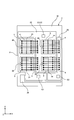
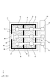
- FIG. 1 is a plan view of the semiconductor module according to the present embodiment.
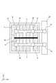
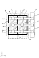
- FIG. 2 is a partially enlarged view of the laminated substrate unit of FIG.
- FIG. 3 is a schematic diagram showing an electric circuit according to the present embodiment.
- the case and the main wiring on the chip are omitted.
- the control wiring is omitted.
- the semiconductor modules shown below are merely examples, and the modules can be changed as appropriate without limitation.
- the longitudinal direction of the semiconductor module (direction in which a plurality of laminated substrates are lined up) is defined as the X direction
- the lateral direction of the semiconductor module is defined as the Y direction
- the height direction (thickness direction of the substrate) is defined as the Z direction.
- the illustrated X, Y, and Z axes are orthogonal to each other and form a right-handed system.
- the X direction may be referred to as a left-right direction
- the Y direction may be referred to as a front-back direction
- the Z direction may be referred to as a vertical direction.
- the heat dissipation surface side (cooler side) of the semiconductor module is referred to as the lower surface side, and the opposite side is referred to as the upper surface side.
- the plan view means the case where the upper surface of the semiconductor module is viewed from the positive side in the Z direction.
- the notation of the direction and the angle may be generally the direction and the angle, and within ⁇ 10 degrees may be allowed.
- the semiconductor module according to this embodiment is applied to a power conversion device such as a power module, and is a power module constituting an inverter circuit.
- the semiconductor module 1 includes a base plate 10, a plurality of laminated substrates 2 arranged on the base plate 10, and a plurality of semiconductor elements 3 arranged on the laminated substrate 2. Consists of including.
- the semiconductor module 1 may also include a case for accommodating the laminated substrate 2 and a plurality of semiconductor elements 3 and a sealing resin (both not shown) filled in the case.
- the base plate 10 is a rectangular plate having an upper surface and a lower surface.
- the base plate 10 functions as a heat sink. Further, the base plate 10 has a rectangular shape in a plan view having a long side in the X direction and a short side in the Y direction.
- the base plate 10 is a metal plate made of, for example, copper, aluminum, an alloy thereof, or the like, and the surface thereof may be plated.
- a rectangular case in a plan view is arranged on the upper surface of the base plate 10.
- the case is formed in a box shape having an opening below the base plate 10 and below so as to cover the plurality of semiconductor elements.
- the case defines a space for accommodating the laminated substrate 2, the semiconductor element, the sealing resin, and the like.
- the external terminal includes a positive electrode terminal (P terminal), a negative electrode terminal (N terminal), and an output terminal (M terminal), and may also include a control terminal.
- the positive electrode terminal, the negative electrode terminal, and the output terminal may be referred to as a main terminal.
- the external terminal may include a plurality of control terminals. Each external terminal is formed by pressing a metal plate such as a copper material, a copper alloy material, an aluminum alloy material, or an iron alloy material.
- the laminated substrate 2 is formed, for example, in a rectangular shape in a plan view.
- the six laminated substrates 2 are arranged side by side in the X direction.
- the laminated substrate 2 is formed by laminating a metal layer and an insulating layer, and is composed of, for example, a DCB (Direct Copper Bonding) substrate, an AMB (Active Metal Brazing) substrate, or a metal base substrate.
- the laminated substrate 2 has an insulating plate 20, a heat radiating plate (not shown) arranged on the lower surface of the insulating plate 20, and a circuit board 21-24 arranged on the upper surface of the insulating plate 20.
- the insulating plate 20 has a predetermined thickness in the Z direction and is formed in a flat plate shape having an upper surface and a lower surface.
- the insulating plate 20 is a ceramic material such as alumina (Al 2 O 3 ), aluminum nitride (AlN), silicon nitride (Si 3 N 4 ), a resin material such as epoxy, or an epoxy resin material using a ceramic material as a filler. It is formed by an insulating material such as.
- the insulating plate 20 may be referred to as an insulating layer or an insulating film.
- the heat radiating plate has a predetermined thickness in the Z direction and is formed so as to cover substantially the entire lower surface of the insulating plate.
- the heat radiating plate is formed of a metal plate having good thermal conductivity such as copper or aluminum.
- a plurality of circuit plates 21-24 are independently formed in an island shape in a state of being electrically insulated from each other. ..
- the three circuit boards 21-23 form the main wiring through which the main current flows.
- the circuit board 24 constitutes a control wiring for control.
- These circuit boards are composed of a metal layer having a predetermined thickness formed of copper foil or the like.
- the circuit board 21-23 may be referred to as a main wiring layer
- the circuit board 24 may be referred to as a control wiring layer.
- the circuit plate 21 is arranged unevenly on the negative side in the X direction on the upper surface of the insulating plate 20.
- the circuit board 21 has an L-shaped plan view extending in the Y direction along one side of the insulating plate 20 and bending the end on the negative side in the Y direction to the positive side in the X direction.
- a pad portion C1 for external connection to which the collector electrode of the upper arm is connected is arranged.
- the pad portion C1 is connected to an external positive potential point (P terminal) of the power supply (see FIG. 3). That is, the circuit board 21 constitutes the main wiring layer of the upper arm.
- the circuit plate 22 is arranged unevenly on the positive side in the X direction on the upper surface of the insulating plate 20.
- the circuit board 22 has an L-shaped plan view extending in the Y direction along one side of the insulating plate 20 and bending the end on the positive side in the Y direction to the negative side in the X direction.
- a pad portion E1C2 for external connection to which the emitter electrode of the upper arm and the collector electrode of the lower arm are connected is arranged.
- the pad portion E1C2 is connected to an external load as an intermediate potential point (M terminal) (see FIG. 3). That is, the circuit board 22 constitutes a part of the main wiring layer of the lower arm.
- the circuit board 23 is arranged on the upper surface of the insulating plate 20 so as to be biased toward the positive side in the X direction with respect to the circuit board 22.
- the circuit board 23 has an L-shaped plan view extending in the Y direction along one side of the insulating plate 20 and bending the end on the negative side in the Y direction to the negative side in the X direction.
- a pad portion E2 for external connection to which the emitter electrode of the lower arm is connected is arranged at the corner of the L-shape of the circuit board 23, a pad portion E2 for external connection to which the emitter electrode of the lower arm is connected is arranged.
- the pad portion E2 is connected to an external positive potential point (N terminal) of the power supply (see FIG. 3). That is, the circuit board 23 constitutes a part of the main wiring layer of the lower arm.
- the circuit plate 24 is arranged unevenly on the negative side in the Y direction on the upper surface of the insulating plate 20.
- the circuit board 24 has an L-shaped plan view extending in the X direction along one side of the insulating plate 20 and having an end portion on the negative side in the X direction slightly bent in the positive side in the Y direction.
- each external terminal is connected to the upper surface of these circuit boards.
- Each end of these external terminals is directly connected to the upper surface of a predetermined circuit board by ultrasonic bonding, laser bonding, or the like, or is connected via a bonding material such as solder or sintered metal.
- the ends of each external terminal are conductively connected to a predetermined circuit board.
- the connection relationship between each external terminal and the circuit board will not be described.
- a semiconductor element 3 is arranged on the upper surface of a predetermined circuit board via a bonding material S (see FIG. 6) such as solder.
- the semiconductor element 3 is formed in a planar rectangular shape (or rectangular shape) by a semiconductor substrate such as silicon (Si), silicon carbide (SiC), or gallium nitride (GaN).
- a switching element such as an IGBT (Insulated Gate Bipolar Transistor), a power MOSFET (Metal Oxide Semiconductor Field Effect Transistor), and a diode such as FWD (Free Wheeling Diode) are used.
- an RC (Reverse Conducting) -IGBT element in which an IGBT and an FWD are integrated is used as the semiconductor element 3
- a power MOSFET element an RB (Reverse Blocking) -IGBT or the like having a sufficient withstand voltage against a reverse bias may be used.
- the shape, number of arrangements, arrangement locations, etc. of the semiconductor element 3 can be appropriately changed.
- the semiconductor element 3 in the present embodiment is a vertical switching element in which a functional element such as a transistor is formed on a semiconductor substrate.
- electrodes are formed on the upper surface and the lower surface, respectively (see FIG. 6).
- the electrode on the upper surface side (top electrode T1) is composed of an emitter electrode (source electrode).
- the lower surface side electrode (bottom surface electrode B1) is composed of a collector electrode (drain electrode).
- the top electrode T1 and the bottom electrode B2 may be referred to as a main electrode.
- a gate pad 30 and a gate runner 31 are formed on the upper surface of the semiconductor element 3 (see FIGS. 5 and 6).
- the gate pad 30 represents the inlet of the main current to the semiconductor element 3.
- the gate pad 30 is formed in a region separated (independent) from the above-mentioned top electrode.
- the gate pad 30 is arranged on the outer peripheral side of the upper surface of the semiconductor element 3. More specifically, the gate pad 30 is arranged in the center of one side of the semiconductor element 3. In FIG. 2, the gate pad 30 is arranged on one side of the semiconductor element 3 located on the negative side in the X direction.
- the gate pad 30 may be referred to as a gate electrode.
- the gate runner 31 constitutes a gate wiring connected to the gate pad 30. That is, the gate runner 31 constitutes a part of the current path for passing a current through the semiconductor element 3.
- the gate runner 31 is formed so as to extend in the Y direction so as to divide the center of the semiconductor element 3 into two in the X direction. The detailed structure on the surface of the gate runner 31 and the semiconductor element 3 will be described later.
- the plurality of semiconductor elements 3 are arranged on the upper surfaces of the circuit boards 21 and 22 via a bonding material (not shown) such as solder. As a result, each bottom electrode of the semiconductor element 3 is conductively connected to the circuit boards 21 and 22. As a result, each external terminal and each semiconductor element are in a conductively connected state.
- two semiconductor elements 3 are arranged on the upper surfaces of the circuit boards 21 and 22, for a total of four semiconductor elements 3.
- the circuit board 21 two semiconductor elements 3 are arranged side by side in the Y direction.
- the two semiconductor elements 3 on the circuit board 21 form an upper arm.
- two semiconductor elements 3 are arranged side by side in the Y direction.
- the two semiconductor elements 3 on the circuit board 22 form a lower arm.
- the upper arm and the lower arm are arranged so as to face each other in the X direction.
- the upper arm is located on the negative side in the X direction
- the lower arm is located on the positive side in the X direction.
- the top electrode of the semiconductor element 3 and the predetermined circuit board are electrically connected by a wiring member 4 such as a wire.
- a wiring member 4 such as a wire.
- the top electrode of the semiconductor element 3 constituting the upper arm is connected to the circuit board 22 via the wiring member 4.
- the upper surface electrode of the semiconductor element 3 constituting the lower arm is electrically connected to the circuit board 23 via the wiring member 4.
- the semiconductor element 3 is connected to a predetermined circuit board by so-called stitch bonding, in which bonding is continuously performed at a plurality of bonding points without cutting a wire at each bonding point.
- the wiring member 4 has two connection points 40 and 41 (see FIGS. 4 and 5) on the upper surface of the semiconductor element 3 and has a predetermined circuit board (circuit board 22 or circuit). It has one connection point 42 (see FIGS. 4 and 5) on the plate 23).
- the number of connection points is not limited to this, and can be changed as appropriate.
- the wiring member 4 is arranged so as to extend in the X direction in a plan view. Further, the wiring member 4 extends so as to form an arch between adjacent connection points when viewed from the Y direction. Although the details will be described later, the wiring member 4 is arranged so as to straddle the gate runner 31 extending in the Y direction. That is, the gate runner 31 is arranged so as to dive under the wiring member 4 between the connection points 40 and 41.
- a plurality of wiring members 4 are arranged for one semiconductor element 3. More specifically, seven wiring members 4 are arranged side by side in the Y direction. The number of wiring members 4 is not limited to this, and can be changed as appropriate.
- a conductor wire (bonding wire) is used for these wiring members 4.
- the material of the conductor wire any one of gold, copper, aluminum, gold alloy, copper alloy, aluminum alloy or a combination thereof can be used. It is also possible to use a member other than the conductor wire as the wiring member 4.
- a ribbon can be used as the wiring member 4.
- the wiring member 4 is not limited to a wire or the like, and may be formed of a ribbon or a metal plate such as a copper material, a copper alloy-based material, an aluminum alloy-based material, or an iron alloy-based material.
- the number of wiring members (main wiring) connected to the top electrode (main electrode) of the semiconductor element will increase as the capacity of the semiconductor module increases.
- the number of wiring members may be limited depending on the arrangement relationship between the main electrode and the gate electrode (gate pad).
- the number of wiring members is small, the amount of heat generated per wiring member becomes large, which may affect the resistance of the semiconductor module.
- the inventor of the present invention came up with the present invention by paying attention to the positional relationship between the internal structure of the semiconductor element, the gate runner on the surface, and the wiring member.
- FIG. 4 is a plan view of the periphery of the semiconductor element according to the reference example.
- FIG. 5 is a plan view of the periphery of the semiconductor element according to the present embodiment.
- the top electrode of the semiconductor element is omitted, and the internal structure (IGBT region and FWD region described later) is described as being represented in a plan view. The actual internal structure is covered by the top electrodes and therefore does not appear on the surface.
- the layout of the internal structure is only partially different, and the configurations basically provided are the same. Therefore, the configurations of the common names are designated by the same reference numerals and the description thereof will be omitted as appropriate.
- the lower arm side will be described as an example. That is, the upper arm side may have the same structure as below.
- the semiconductor element 3 is an RC-IGBT element that integrates an IGBT and an FWD.
- the RC-IGBT element has a band-shaped IGBT region 3a and an FWD region 3b below the top electrode in a plan view.
- the semiconductor element 3 has a plurality of IGBT regions 3a extending in the Y direction and a plurality of FWD regions 3b extending in the Y direction.
- the IGBT region 3a and the FWD region 3b are arranged side by side alternately in the X direction.
- four IGBT regions 3a and three FWD regions 3b are arranged.
- the gate pad 30 is arranged on one side of the semiconductor element 3 located on the negative side in the X direction. That is, the gate pad 30 is unevenly arranged on one side located on the outer peripheral edge of the semiconductor element 3. Further, a gate runner 31 connected to the gate pad 30 is arranged on the upper surface of the semiconductor element 3.
- the gate runner 31 extends from the gate pad 30 located on the negative side in the X direction toward the positive side in the X direction.
- the gate runner 31 divides the center of the upper surface of the semiconductor element 3 into two in the Y direction.
- the extending direction of the gate runner 31 and the extending direction of the IGBT region 3a and the FWD region 3b are orthogonal to each other.
- circuit board 23 is arranged outside the side facing one side of the semiconductor element 3 in which the gate pad 30 is arranged. That is, the circuit board 23 is arranged on the opposite side of the gate pad 30 with the other side of the semiconductor element 3 interposed therebetween.
- the wiring member 4 has two connection points 40 and 41 on the upper surface of the semiconductor element 3 and one connection point 42 on the circuit board 23. Further, the wiring member 4 extends in the X direction in a plan view. The wiring member 4 extends in parallel with the gate runner 31. Further, the extending direction of the wiring member 4 and the extending direction of the IGBT region 3a and the FWD region 3b are orthogonal to each other.
- two wiring members 4 extending in the X direction are arranged side by side in the Y direction.
- the wiring member 4 cannot arrange the connection point so as to overlap the gate runner 31.
- the wiring member 4 and the gate runner 31 are in parallel. Therefore, if the wiring member 4 is arranged so as to avoid the gate runner 31, the number of the wiring members 4 is limited.
- the extending direction of the gate runner 31 is parallel to the extending direction of the IGBT region 3a and the FWD region 3b. In this case, it may be difficult for the current to flow evenly from the gate runner to each region. As a result, a current imbalance occurs and the switching timing tends to shift.
- the gate runner 31 is formed in a rectangular frame shape surrounding the entire outer peripheral edge of the semiconductor element 3. Specifically, the gate runner 31 has an outer peripheral portion 32 and a straight line portion 33.
- the outer peripheral portion 32 extends from the gate pad 30 along the outer peripheral edge of the semiconductor element 3. More specifically, the outer peripheral portion 32 extends from both ends of the gate pad 30 in the Y direction along the outer peripheral edge of the semiconductor element 3 and is rectangular so as to surround the outer peripheral edge of the semiconductor element 3 (the outer peripheral edge of the upper surface electrode). It is formed in a frame shape.
- the straight line portion 33 connects one sides of the outer peripheral portions 32 facing each other in the Y direction at the center in the X direction. Further, the straight line portion 33 extends in the Y direction so as to divide the center of the semiconductor element 3. That is, the straight line portion 33 divides the upper surface (upper surface electrode) of the semiconductor element into one side (negative side in the X direction) and the other side (positive side in the X direction).
- the outer peripheral portion 32 is not limited to the configuration that surrounds the entire outer peripheral edge of the semiconductor element 3.
- the outer peripheral portion 32 may be on at least one side (negative side in the X direction), that is, on the negative side in the X direction with respect to the straight portion 33.
- the gate runner 31 (outer peripheral portion 32 and straight portion 33) includes a gate wiring layer 34 and an insulating film 35.
- the gate wiring layer 34 is formed independently of the top electrode T1, and is composed of, for example, a metal layer made of the same material as the top electrode T1.
- the insulating film 35 covers the gate wiring layer 34, and is formed of, for example, a resin such as polyimide.
- the insulating film 35 covers the upper part of the gate wiring layer 34 and also covers the edge portion of the upper surface electrode T1. Therefore, the insulating film 35 has an outer surface shape that bulges upward from the gate wiring layer 34 and the upper surface electrode T1.
- the wiring member 4 extends in the X direction in a plan view.
- the wiring member 4 has two connection points 40 and 41 on the upper surface of the semiconductor element 3 and one connection point 42 on the circuit board 23.
- the plurality of wiring members 4 have at least one connection point on the upper surface of the semiconductor element 3 in the region on one side and the region on the other side divided by the straight line portion 33.
- each connection point overlaps both the IGBT region 3a and the FWD region 3b.
- the straight line portion 33 extends so as to go under the wiring member 4. That is, the wiring member 4 is arranged so as to straddle the upper part of the straight line portion 33. Specifically, the wiring member 4 further includes a first arch portion 4a and a second arch portion 4b (see FIG. 6).
- the first arch portion 4a is connected to the connection points 40 and 41 and is formed in an upwardly convex arch shape between the connection points 40 and 41.
- the second arch portion 4b is connected to the connection points 41 and 42, and is formed in an upwardly convex arch shape between the connection points 41 and 42.
- the first arch portion 4a straddles the upper part of a part of the gate runner 31 (straight line portion 33).
- the second arch portion 4b straddles the upper part of the part of the gate runner 31 (a part of the outer peripheral portion 32).
- the present embodiment it is possible to secure the number of connections of the wiring member 4 (main wiring) and increase the number of connection points 40 and 41 of the wiring member 4 with respect to the top electrode. As a result, the amount of heat generated per connection point can be reduced, and the bias in heat distribution can be reduced. Therefore, it is possible to improve the resistance of the semiconductor module 1 to heat.
- the semiconductor element 3 has a rectangular shape in a plan view and is arranged on one side of the rectangular shape (on one side corresponding to the negative side in the X direction, which is one side of the semiconductor element 3). It has a pad 30. Further, the circuit board 23 (another circuit board) sandwiches the other side of the semiconductor element 3 (one side corresponding to the positive side in the X direction, which is the other side of the semiconductor element 3) with respect to the circuit board 22 of the gate pad 30. It is located on the other side. According to this configuration, the control wiring (not shown) connected to the gate pad 30 can be arranged on one side, the negative side in the X direction. On the other hand, the wiring member 4 which is the main wiring can be arranged on the positive side in the X direction, which is the other side of the control wiring. That is, the control wiring and the main wiring can be arranged separately without overlapping.
- the semiconductor element 3 is an RC-IGBT element in which an IGBT and an FWD are integrated.
- the RC-IGBT element has a band-shaped IGBT region 3a and an FWD region 3b below the top electrode in a plan view.
- the semiconductor element 3 has a plurality of IGBT regions 3a extending in the X direction and a plurality of FWD regions 3b extending in the X direction.
- the IGBT region 3a and the FWD region 3b are arranged side by side alternately in the Y direction.
- four IGBT regions 3a and three FWD regions 3b are arranged.
- the IGBT region 3a and the FWD region 3b extend in the direction (X direction) intersecting the straight line portion 33 of the gate runner 31. That is, the IGBT region 3a, the FWD region 3b, and the wiring member 4 extend in the same X direction in a plan view.
- the extending direction of the IGBT region 3a and the FWD region 3b may be referred to as a trench direction.
- the RC-IGBT element In the RC-IGBT element, current easily flows in the trench direction. That is, the RC-IGBT element has directivity in the current flow direction. Specifically, the main current flows from the gate pad 30 to the outer peripheral portion 32 and the straight portion 33 of the gate runner 31. Then, the main current flows from the straight line portion 33 through each IGBT region 3a and FWD region 3b along the trench direction on both sides in the X direction.
- the wiring member 4 through which the main current flows extends in the same direction as the trench direction, the direction in which the main current flows is combined in one direction (X direction) for the entire module. As a result, the current flow distribution becomes uniform, noise and oscillation can be suppressed, and local heat generation can be prevented.
- the IGBT region 3a has a width larger than that of the FWD region 3b. According to this configuration, the current sharing in each region can be leveled, and abnormal heating or destruction of either one can be suppressed.
- the wiring member 4 has at least one connection point that overlaps both the IGBT region 3a and the FWD region 3b in a plan view.
- the on / off timing is opposite between the IGBT and the FWD, and the current flow timing is also different. If the connection points overlap only one area, local heat generation may occur. Therefore, it is possible to make the heat distribution uniform and suppress local heat generation by overlapping the connection points in both regions.
- the gate runner 31 (straight line portion 33) so as to dive under the arch-shaped wiring member 4, the number of wiring connections is secured and heat is repelled. It is possible to improve resistance.
- FIGS. 8 to 12 are plan views of the periphery of the semiconductor element according to the modified example.
- the wiring member 4 extends in parallel with the extending direction of the IGBT region 3a and the FWD region 3b has been described, but the configuration is not limited to this.
- the wiring member 4 may be inclined with respect to the extending direction of the IGBT region 3a and the FWD region 3b in a plan view. That is, the wiring member 4 only needs to straddle the upper part of the gate runner 31 (straight line portion 33).
- connection point of the wiring member 4 overlaps the IGBT region 3a and the FWD region 3b in a plan view
- the configuration is not limited to this.
- one wiring member may have only one connection point on the semiconductor element 3.
- a wiring member 5 (second wiring member) shorter than the wiring member 4 is arranged.
- the wiring member 4 straddles the straight portion 33 and above a part of the outer peripheral portion 32 located on the negative side in the X direction.
- the connection point 40 of the wiring member 4 is located on the negative side in the X direction with respect to the straight line portion 33.
- the wiring member 5 does not straddle the upper part of the straight line portion 33, but straddles the upper part of the outer peripheral portion 32 located on the negative side in the X direction.
- the connection point 51 of the wiring member 5 is located on the positive side in the X direction with respect to the straight line portion 33. Further, the connection point 52 of the wiring member member 5 is arranged on the circuit board 23.
- the present invention is not limited to this configuration.
- the number of connection points of the wiring members 4 and 5 may be larger on the positive side in the X direction on the other side than on the negative side in the X direction on one side.
- connection points 40 to 42 may be arranged in each divided region. Further, the connection point 43, which is an end portion of the wiring member 4, is arranged on the circuit board 23.
- FIG. 13 is a plan view of the periphery of the semiconductor element according to the second embodiment.
- FIG. 14 is a partially enlarged view of FIG.
- FIG. 15 is a plan view of the periphery of the semiconductor element according to the modified example of the second embodiment.
- the common configurations are designated by the same reference numerals and the description thereof will be omitted as appropriate.
- heat dissipation occurs in the vicinity of the chip even in a short time of about several msec required to start the operation of the semiconductor module.
- heat dissipation occurs in the vicinity of the chip even in a short time of about several msec required to start the operation of the semiconductor module.
- heat dissipation occurs in the vicinity of the chip even in a short time of about several msec required to start the operation of the semiconductor module.
- heat dissipated On the back surface side of the chip, heat is dissipated via the solder and the insulating substrate, and on the front surface side of the chip, heat is dissipated via the wiring member (bonding wire).
- connection point bonding point
- the IGBT region and the FWD region are formed in a band shape extending in a predetermined direction as described above. Therefore, in a short time of about several msec at the rising edge, the heat is not dissipated on the entire surface of the chip, but is dissipated unevenly in a band shape. That is, there is a problem that the heat dissipation area in a short time becomes small and the transient thermal resistance becomes large as compared with the case where the IGBT and the FWD are separate bodies.
- the present inventor further focused on the heat dissipation distribution and the layout of the wiring member in the RC-IGBT element, and came up with the present invention.
- a plurality of IGBT regions 3a and FWD regions 3b extending in a band shape along the Y direction are arranged alternately side by side.
- the gate runner 31 is arranged so as to surround the outer periphery of the semiconductor element 3.
- the gate runner 31 is formed in a rectangular frame shape that surrounds the entire outer peripheral edge of the semiconductor element 3.
- the gate runner 31 has an outer peripheral portion 32 and a straight line portion 33.
- the outer peripheral portion 32 extends from the gate pad 30 along the outer peripheral edge of the semiconductor element 3. More specifically, the outer peripheral portion 32 extends from both ends of the gate pad 30 in the Y direction along the outer peripheral edge of the semiconductor element 3 and is rectangular so as to surround the outer peripheral edge of the semiconductor element 3 (the outer peripheral edge of the upper surface electrode). It is formed in a frame shape.
- the straight line portion 33 connects one sides of the outer peripheral portions 32 facing each other in the Y direction at the center in the X direction. Further, the straight line portion 33 extends in the Y direction so as to divide the center of the semiconductor element 3. That is, the straight line portion 33 divides the upper surface (upper surface electrode) of the semiconductor element into one side (negative side in the X direction) and the other side (positive side in the X direction).
- the straight line portion 33 is referred to as a first straight line portion 33
- the two straight line portions of the outer peripheral portion 32 arranged opposite to the first straight line portion 33 are referred to as a second straight line portion 32a.
- the second straight line portion 32a is composed of a part of the outer peripheral portion 32 extending from the gate pad 30 along the outer peripheral edge of the semiconductor element 3.
- Such an outer peripheral portion 32 constitutes a heat-resistant structural portion of the semiconductor element 3.
- the first straight line portion 33 is connected to the outer peripheral portion 32 and extends so as to divide the center of the semiconductor element 3. Further, the first straight line portion 33 is located at the center between the two second straight line portions 32a.
- the first straight line portion 33 and the two second straight line portions 32a are parallel to each other along the Y direction and extend in a direction intersecting the extending direction (X direction) of the IGBT region 3a and the FWD region 3b. ing.
- the wiring member 4 extends in the X direction above the semiconductor element 3 and is arranged so as to straddle the upper part of the first straight line portion 33 and the second straight line portion 32a. As described above, the wiring member 4 is electrically connected to the main electrode by stitch bonding with a predetermined circuit board 23, and has a plurality of connection points 40, 41, 42 (bonding points). Further, in FIG. 13, three wiring members 4 are arranged side by side in the Y direction.
- connection point 40 is arranged in the rectangular area on the negative side in the X direction in the rectangular area in the plan view surrounded by the gate runner 31. Further, the connection point 40 is arranged so as to overlap the first straight line portion 33 and the center line C located equidistant from the second straight line portion or 32a in a plan view.
- the center line C extends parallel to the first straight line portion 33 and the second straight line portion 32a between the first straight line portion 33 and the second straight line portion 32a.
- connection point 41 is arranged in a rectangular area on the positive side in the X direction in the rectangular area in a plan view surrounded by the gate runner 31. Like the connection point 40, the connection point 41 is also arranged so as to overlap the first straight line portion 33 and the center line C located equidistant from the second straight line portion or 32a in a plan view.
- connection points 40 and 41 are provided at positions equidistant from the gate runner 31 (first straight line portion 33, second straight line portion 32a) extending in the Y direction to make the heat dissipation area most uniform. It is possible. As a result, it is possible to reduce the transient thermal resistance and further reduce the temperature ripple.
- connection points 40 and 41 overlap the IGBT region 3a in a plan view. Since the current flows from the IGBT region 3a at the start of operation of the semiconductor module, it is possible to suppress the transient thermal resistance in a short time and prevent local heat generation at the time of rising.
- connection points 40 and 41 are formed in a rectangular shape (almost a square) in a plan view has been described, but the present invention is not limited to this configuration.
- the connection points 40 and 41 may have an elliptical shape that is long in the extending direction (X direction) of the wiring member 4 in a plan view.
- connection points 40 and 41 overlap (match)
- the present invention is not limited to this, and changes may be made as appropriate. It is possible.
- at least a part of the connection points 40 and 41 may overlap with the center line C, and the center lines C1 and the center line C in the X direction (longitudinal direction) of the connection points 40 and 41 are It does not necessarily have to match.
- connection points 40 and 41 overlap the IGBT region 3a in a plan view
- the configuration is not limited to this.
- all or most of the connection points 40 and 41 may be arranged so as to overlap the FWD region 3b in a plan view. In this case, it is possible to suppress local heat generation when a current flows in the FWD region 3b due to the counter electromotive force.
- the number and layout of the circuit boards are not limited to the above configuration and can be changed as appropriate.
- the laminated substrate 2 and the semiconductor element are formed in a rectangular shape or a rectangular shape in a plan view, but the configuration is not limited to this.
- the laminated substrate 2 and the semiconductor element may be formed in a polygonal shape other than the above.
- the present embodiment is not limited to the above-described embodiment and modification, and may be variously changed, replaced, or modified without departing from the spirit of the technical idea. Further, if the technical idea can be realized in another way by the advancement of the technology or another technology derived from it, it may be carried out by the method. Therefore, the claims cover all embodiments that may be included within the scope of the technical idea.
- the semiconductor module according to the above embodiment has a laminated substrate in which a plurality of circuit plates are arranged on the upper surface of an insulating plate, and a main electrode, a gate pad, and the gate pad on the upper surface, which are arranged on a predetermined circuit plate.
- a semiconductor element having an electrically connected gate runner and a wiring member for electrically connecting the main electrode and another circuit board are provided, and the gate runner has the main electrode on one side and the other side.
- the wiring member is arranged so as to straddle the upper part of the gate runner.
- the semiconductor element has a rectangular shape in a plan view
- the gate pad is arranged on one side of the semiconductor element corresponding to the one side
- the other The circuit board is arranged on the opposite side of the gate pad with the other side corresponding to the other side of the semiconductor element interposed therebetween, and the gate runner and the wiring member intersect in a plan view.
- the gate runner extends so as to divide the center of the upper surface of the semiconductor element, and divides the main electrode into at least two.
- the wiring member is composed of a plurality of conductor wires.
- a second wiring member which is shorter than the wiring member and has at least one connection point on the other side is further provided.
- the wiring member has at least one connection point on one side of the upper surface of the semiconductor element.
- the number of connection points between the wiring member and the second wiring member is larger on the other side than on the one side.
- the number of connection points between the wiring member and the second wiring member is the same on one side and the other side.
- the semiconductor element is an RC (Reverse Conducting) -IGBT element in which an IGBT (Insulated Gate Bipolar Transistor) and an FWD (Free Wheeling Diode) are integrated, and is viewed in a plan view. It further has a plurality of IGBT regions and FWD regions extending in a band shape, and the plurality of the IGBT regions and the FWD regions are arranged alternately.
- RC Reverse Conducting
- IGBT Insulated Gate Bipolar Transistor
- FWD Free Wheeling Diode
- the IGBT region and the FWD region extend in a direction intersecting with the gate runner.
- the IGBT region has a width larger than that of the FWD region.
- the wiring member is inclined with respect to the extending direction of the IGBT region and the FWD region in a plan view.
- the wiring member has at least one connection point that overlaps both the IGBT region and the FWD region in a plan view.
- the semiconductor element has a rectangular shape in a plan view, further has a gate pad arranged on one side of the rectangular shape, and the gate runner is the gate pad. It has an outer peripheral portion extending from the outer peripheral edge of the semiconductor element, and a straight line portion connected to the outer peripheral portion and extending so as to divide the center of the semiconductor element, and the wiring member includes the straight line portion and /. Alternatively, it is arranged so as to straddle the upper part of the outer peripheral portion.
- the semiconductor module according to the above embodiment has a laminated substrate in which a plurality of circuit plates are arranged on the upper surface of the insulating plate, and a main electrode, a gate pad, and the gate on the upper surface, which are arranged on a predetermined circuit plate.
- a semiconductor element having a gate runner electrically connected to a pad and a wiring member for electrically connecting the main electrode and another circuit board are provided, and the semiconductor element is an IGBT (Insulated Gate Bipolar Transistor). It is an RC (Reverse Conducting) -IGBT element that integrates and FWD (Free Wheeling Diode), and further has a plurality of IGBT regions and FWD regions that extend in a band shape and are alternately arranged in a plan view.
- a first straight portion extending by dividing the main electrode into one side and the other side, and a second straight portion arranged facing the first straight portion and extending along the outer peripheral edge of the semiconductor element.
- the first straight portion and the second straight portion extend in a direction intersecting the IGBT region and the FWD region, and the wiring member straddles at least above the first straight portion.
- At least a part of the connection points to the main electrodes overlaps the center line located at equal distances from the first straight line portion and the second straight line portion in a plan view.
- the center line is parallel to the first straight line portion and the second straight line portion between the first straight line portion and the second straight line portion. Extends to.
- the semiconductor element has a rectangular shape in a plan view
- the gate pad is arranged on one side of the rectangular shape
- the second straight line portion is the above. It is composed of a part of the outer peripheral portion extending from the gate pad along the outer peripheral edge of the semiconductor element, the outer peripheral portion constitutes the heat-resistant structure portion of the semiconductor element, and the first straight line portion is on the outer peripheral portion. It is continuous and extends so as to divide the center of the semiconductor element.
- the wiring member extends in a direction intersecting the first straight line portion in a plan view, and the connection point of the wiring member is the wiring member in a plan view. It has a long oval shape in the extending direction of.
- connection point of the wiring member overlaps with the IGBT region in a plan view.
- connection point of the wiring member overlaps with the FWD region in a plan view.
- the present invention has the effect of securing the number of main wiring connections and improving the heat resistance, and is particularly useful for semiconductor modules.
Landscapes
- Engineering & Computer Science (AREA)
- Microelectronics & Electronic Packaging (AREA)
- Power Engineering (AREA)
- Computer Hardware Design (AREA)
- Physics & Mathematics (AREA)
- Condensed Matter Physics & Semiconductors (AREA)
- General Physics & Mathematics (AREA)
- Chemical & Material Sciences (AREA)
- Ceramic Engineering (AREA)
- Materials Engineering (AREA)
- Inverter Devices (AREA)
- Cooling Or The Like Of Semiconductors Or Solid State Devices (AREA)
Abstract
Selon l'invention, le nombre de connexions d'un câblage principal est garanti, et la résistance à la chaleur est améliorée. Plus précisément, l'invention concerne un module à semi-conducteurs (1) qui est équipé : d'un substrat stratifié (2) dans lequel une pluralité de cartes de circuits imprimés (22, 23) est disposée sur une face supérieure d'une plaque d'isolation (20) ; d'un élément à semi-conducteurs (3) qui est disposé sur une carte de circuits imprimés (22) prédéfinie, et qui possède sur sa face supérieure une électrode principale, une pastille de grille (30) et un canal de grille (31) électriquement connecté à la pastille de grille (30) ; et d'un élément câblage (4) électriquement connecté à l'électrode principale et à l'autre carte de circuits imprimés (23). Le canal de grille (31) se prolonge de manière à diviser l'électrode principale en un côté et en un autre côté. L'élément câblage (4) est disposé de manière à enjamber le canal de grille (31) par le dessus.
Priority Applications (4)
| Application Number | Priority Date | Filing Date | Title |
|---|---|---|---|
| JP2022534960A JP7294540B2 (ja) | 2020-07-07 | 2021-06-07 | 半導体モジュール |
| DE112021000198.1T DE112021000198T5 (de) | 2020-07-07 | 2021-06-07 | Halbleitermodul |
| CN202180008032.4A CN114902407A (zh) | 2020-07-07 | 2021-06-07 | 半导体模块 |
| US17/855,782 US20220336403A1 (en) | 2020-07-07 | 2022-06-30 | Semiconductor module |
Applications Claiming Priority (2)
| Application Number | Priority Date | Filing Date | Title |
|---|---|---|---|
| JP2020-117233 | 2020-07-07 | ||
| JP2020117233 | 2020-07-07 |
Related Child Applications (1)
| Application Number | Title | Priority Date | Filing Date |
|---|---|---|---|
| US17/855,782 Continuation US20220336403A1 (en) | 2020-07-07 | 2022-06-30 | Semiconductor module |
Publications (1)
| Publication Number | Publication Date |
|---|---|
| WO2022009582A1 true WO2022009582A1 (fr) | 2022-01-13 |
Family
ID=79552410
Family Applications (1)
| Application Number | Title | Priority Date | Filing Date |
|---|---|---|---|
| PCT/JP2021/021617 WO2022009582A1 (fr) | 2020-07-07 | 2021-06-07 | Module à semi-conducteurs |
Country Status (5)
| Country | Link |
|---|---|
| US (1) | US20220336403A1 (fr) |
| JP (1) | JP7294540B2 (fr) |
| CN (1) | CN114902407A (fr) |
| DE (1) | DE112021000198T5 (fr) |
| WO (1) | WO2022009582A1 (fr) |
Citations (4)
| Publication number | Priority date | Publication date | Assignee | Title |
|---|---|---|---|---|
| US5767567A (en) * | 1996-09-10 | 1998-06-16 | Magemos Corporation | Design of device layout for integration with power mosfet packaging to achieve better lead wire connections and lower on resistance |
| WO2015050262A1 (fr) * | 2013-10-04 | 2015-04-09 | 富士電機株式会社 | Dispositif à semi-conducteurs |
| WO2019159391A1 (fr) * | 2018-02-14 | 2019-08-22 | 富士電機株式会社 | Dispositif à semi-conducteur |
| WO2020059285A1 (fr) * | 2018-09-20 | 2020-03-26 | 富士電機株式会社 | Dispositif à semi-conducteur |
Family Cites Families (3)
| Publication number | Priority date | Publication date | Assignee | Title |
|---|---|---|---|---|
| JP2010016103A (ja) | 2008-07-02 | 2010-01-21 | Panasonic Corp | 半導体装置 |
| WO2018225571A1 (fr) | 2017-06-09 | 2018-12-13 | 富士電機株式会社 | Dispositif à semi-conducteur et procédé de fabrication d'un dispositif à semi-conducteur |
| JP7326750B2 (ja) | 2019-01-18 | 2023-08-16 | 大日本印刷株式会社 | 包装体 |
-
2021
- 2021-06-07 JP JP2022534960A patent/JP7294540B2/ja active Active
- 2021-06-07 DE DE112021000198.1T patent/DE112021000198T5/de active Pending
- 2021-06-07 CN CN202180008032.4A patent/CN114902407A/zh active Pending
- 2021-06-07 WO PCT/JP2021/021617 patent/WO2022009582A1/fr active Application Filing
-
2022
- 2022-06-30 US US17/855,782 patent/US20220336403A1/en active Pending
Patent Citations (4)
| Publication number | Priority date | Publication date | Assignee | Title |
|---|---|---|---|---|
| US5767567A (en) * | 1996-09-10 | 1998-06-16 | Magemos Corporation | Design of device layout for integration with power mosfet packaging to achieve better lead wire connections and lower on resistance |
| WO2015050262A1 (fr) * | 2013-10-04 | 2015-04-09 | 富士電機株式会社 | Dispositif à semi-conducteurs |
| WO2019159391A1 (fr) * | 2018-02-14 | 2019-08-22 | 富士電機株式会社 | Dispositif à semi-conducteur |
| WO2020059285A1 (fr) * | 2018-09-20 | 2020-03-26 | 富士電機株式会社 | Dispositif à semi-conducteur |
Also Published As
| Publication number | Publication date |
|---|---|
| JPWO2022009582A1 (fr) | 2022-01-13 |
| DE112021000198T5 (de) | 2022-08-18 |
| JP7294540B2 (ja) | 2023-06-20 |
| US20220336403A1 (en) | 2022-10-20 |
| CN114902407A (zh) | 2022-08-12 |
Similar Documents
| Publication | Publication Date | Title |
|---|---|---|
| US7271477B2 (en) | Power semiconductor device package | |
| WO2013172291A1 (fr) | Dispositif à semi-conducteurs de module de puissance | |
| JP7428018B2 (ja) | 半導体モジュール | |
| US11398448B2 (en) | Semiconductor module | |
| US11923266B2 (en) | Semiconductor module circuit structure | |
| JP7006812B2 (ja) | 半導体装置 | |
| US11581252B2 (en) | Semiconductor module and wire bonding method | |
| US11309276B2 (en) | Semiconductor module | |
| JP7379886B2 (ja) | 半導体装置 | |
| JP7414073B2 (ja) | 半導体モジュール | |
| US11545409B2 (en) | Semiconductor module having block electrode bonded to collector electrode and manufacturing method thereof | |
| JP7322654B2 (ja) | 半導体モジュール | |
| JP7428019B2 (ja) | 半導体モジュール | |
| JP2021158232A (ja) | 半導体モジュール | |
| WO2022009582A1 (fr) | Module à semi-conducteurs | |
| US11984386B2 (en) | Semiconductor device | |
| JP7396118B2 (ja) | 半導体モジュール | |
| JP7491043B2 (ja) | 半導体モジュール | |
| JPWO2020149225A1 (ja) | 半導体装置 | |
| JP2021180234A (ja) | 半導体モジュール | |
| WO2024095710A1 (fr) | Module semi-conducteur | |
| JP2023156806A (ja) | 半導体モジュール | |
| JP2023040345A (ja) | 半導体モジュール及び半導体モジュールの製造方法 | |
| JP2021190553A (ja) | 半導体モジュール | |
| JP2023128114A (ja) | 半導体装置 |
Legal Events
| Date | Code | Title | Description |
|---|---|---|---|
| 121 | Ep: the epo has been informed by wipo that ep was designated in this application |
Ref document number: 21838752 Country of ref document: EP Kind code of ref document: A1 |
|
| ENP | Entry into the national phase |
Ref document number: 2022534960 Country of ref document: JP Kind code of ref document: A |
|
| 122 | Ep: pct application non-entry in european phase |
Ref document number: 21838752 Country of ref document: EP Kind code of ref document: A1 |