WO2022004181A1 - 炭化珪素エピタキシャル基板および炭化珪素エピタキシャル基板の製造方法 - Google Patents
炭化珪素エピタキシャル基板および炭化珪素エピタキシャル基板の製造方法 Download PDFInfo
- Publication number
- WO2022004181A1 WO2022004181A1 PCT/JP2021/019171 JP2021019171W WO2022004181A1 WO 2022004181 A1 WO2022004181 A1 WO 2022004181A1 JP 2021019171 W JP2021019171 W JP 2021019171W WO 2022004181 A1 WO2022004181 A1 WO 2022004181A1
- Authority
- WO
- WIPO (PCT)
- Prior art keywords
- silicon carbide
- carbide epitaxial
- epitaxial layer
- substrate
- reaction chamber
- Prior art date
- Legal status (The legal status is an assumption and is not a legal conclusion. Google has not performed a legal analysis and makes no representation as to the accuracy of the status listed.)
- Ceased
Links
Images





Classifications
-
- H—ELECTRICITY
- H10—SEMICONDUCTOR DEVICES; ELECTRIC SOLID-STATE DEVICES NOT OTHERWISE PROVIDED FOR
- H10P—GENERIC PROCESSES OR APPARATUS FOR THE MANUFACTURE OR TREATMENT OF DEVICES COVERED BY CLASS H10
- H10P14/00—Formation of materials, e.g. in the shape of layers or pillars
- H10P14/20—Formation of materials, e.g. in the shape of layers or pillars of semiconductor materials
- H10P14/29—Formation of materials, e.g. in the shape of layers or pillars of semiconductor materials characterised by the substrates
- H10P14/2901—Materials
- H10P14/2902—Materials being Group IVA materials
- H10P14/2904—Silicon carbide
-
- C—CHEMISTRY; METALLURGY
- C23—COATING METALLIC MATERIAL; COATING MATERIAL WITH METALLIC MATERIAL; CHEMICAL SURFACE TREATMENT; DIFFUSION TREATMENT OF METALLIC MATERIAL; COATING BY VACUUM EVAPORATION, BY SPUTTERING, BY ION IMPLANTATION OR BY CHEMICAL VAPOUR DEPOSITION, IN GENERAL; INHIBITING CORROSION OF METALLIC MATERIAL OR INCRUSTATION IN GENERAL
- C23C—COATING METALLIC MATERIAL; COATING MATERIAL WITH METALLIC MATERIAL; SURFACE TREATMENT OF METALLIC MATERIAL BY DIFFUSION INTO THE SURFACE, BY CHEMICAL CONVERSION OR SUBSTITUTION; COATING BY VACUUM EVAPORATION, BY SPUTTERING, BY ION IMPLANTATION OR BY CHEMICAL VAPOUR DEPOSITION, IN GENERAL
- C23C16/00—Chemical coating by decomposition of gaseous compounds, without leaving reaction products of surface material in the coating, i.e. chemical vapour deposition [CVD] processes
- C23C16/02—Pretreatment of the material to be coated
-
- C—CHEMISTRY; METALLURGY
- C23—COATING METALLIC MATERIAL; COATING MATERIAL WITH METALLIC MATERIAL; CHEMICAL SURFACE TREATMENT; DIFFUSION TREATMENT OF METALLIC MATERIAL; COATING BY VACUUM EVAPORATION, BY SPUTTERING, BY ION IMPLANTATION OR BY CHEMICAL VAPOUR DEPOSITION, IN GENERAL; INHIBITING CORROSION OF METALLIC MATERIAL OR INCRUSTATION IN GENERAL
- C23C—COATING METALLIC MATERIAL; COATING MATERIAL WITH METALLIC MATERIAL; SURFACE TREATMENT OF METALLIC MATERIAL BY DIFFUSION INTO THE SURFACE, BY CHEMICAL CONVERSION OR SUBSTITUTION; COATING BY VACUUM EVAPORATION, BY SPUTTERING, BY ION IMPLANTATION OR BY CHEMICAL VAPOUR DEPOSITION, IN GENERAL
- C23C16/00—Chemical coating by decomposition of gaseous compounds, without leaving reaction products of surface material in the coating, i.e. chemical vapour deposition [CVD] processes
- C23C16/22—Chemical coating by decomposition of gaseous compounds, without leaving reaction products of surface material in the coating, i.e. chemical vapour deposition [CVD] processes characterised by the deposition of inorganic material, other than metallic material
- C23C16/30—Deposition of compounds, mixtures or solid solutions, e.g. borides, carbides, nitrides
- C23C16/42—Silicides
-
- C—CHEMISTRY; METALLURGY
- C30—CRYSTAL GROWTH
- C30B—SINGLE-CRYSTAL GROWTH; UNIDIRECTIONAL SOLIDIFICATION OF EUTECTIC MATERIAL OR UNIDIRECTIONAL DEMIXING OF EUTECTOID MATERIAL; REFINING BY ZONE-MELTING OF MATERIAL; PRODUCTION OF A HOMOGENEOUS POLYCRYSTALLINE MATERIAL WITH DEFINED STRUCTURE; SINGLE CRYSTALS OR HOMOGENEOUS POLYCRYSTALLINE MATERIAL WITH DEFINED STRUCTURE; AFTER-TREATMENT OF SINGLE CRYSTALS OR A HOMOGENEOUS POLYCRYSTALLINE MATERIAL WITH DEFINED STRUCTURE; APPARATUS THEREFOR
- C30B25/00—Single-crystal growth by chemical reaction of reactive gases, e.g. chemical vapour-deposition growth
- C30B25/02—Epitaxial-layer growth
- C30B25/14—Feed and outlet means for the gases; Modifying the flow of the reactive gases
-
- C—CHEMISTRY; METALLURGY
- C30—CRYSTAL GROWTH
- C30B—SINGLE-CRYSTAL GROWTH; UNIDIRECTIONAL SOLIDIFICATION OF EUTECTIC MATERIAL OR UNIDIRECTIONAL DEMIXING OF EUTECTOID MATERIAL; REFINING BY ZONE-MELTING OF MATERIAL; PRODUCTION OF A HOMOGENEOUS POLYCRYSTALLINE MATERIAL WITH DEFINED STRUCTURE; SINGLE CRYSTALS OR HOMOGENEOUS POLYCRYSTALLINE MATERIAL WITH DEFINED STRUCTURE; AFTER-TREATMENT OF SINGLE CRYSTALS OR A HOMOGENEOUS POLYCRYSTALLINE MATERIAL WITH DEFINED STRUCTURE; APPARATUS THEREFOR
- C30B25/00—Single-crystal growth by chemical reaction of reactive gases, e.g. chemical vapour-deposition growth
- C30B25/02—Epitaxial-layer growth
- C30B25/16—Controlling or regulating
-
- C—CHEMISTRY; METALLURGY
- C30—CRYSTAL GROWTH
- C30B—SINGLE-CRYSTAL GROWTH; UNIDIRECTIONAL SOLIDIFICATION OF EUTECTIC MATERIAL OR UNIDIRECTIONAL DEMIXING OF EUTECTOID MATERIAL; REFINING BY ZONE-MELTING OF MATERIAL; PRODUCTION OF A HOMOGENEOUS POLYCRYSTALLINE MATERIAL WITH DEFINED STRUCTURE; SINGLE CRYSTALS OR HOMOGENEOUS POLYCRYSTALLINE MATERIAL WITH DEFINED STRUCTURE; AFTER-TREATMENT OF SINGLE CRYSTALS OR A HOMOGENEOUS POLYCRYSTALLINE MATERIAL WITH DEFINED STRUCTURE; APPARATUS THEREFOR
- C30B25/00—Single-crystal growth by chemical reaction of reactive gases, e.g. chemical vapour-deposition growth
- C30B25/02—Epitaxial-layer growth
- C30B25/18—Epitaxial-layer growth characterised by the substrate
- C30B25/20—Epitaxial-layer growth characterised by the substrate the substrate being of the same materials as the epitaxial layer
-
- C—CHEMISTRY; METALLURGY
- C30—CRYSTAL GROWTH
- C30B—SINGLE-CRYSTAL GROWTH; UNIDIRECTIONAL SOLIDIFICATION OF EUTECTIC MATERIAL OR UNIDIRECTIONAL DEMIXING OF EUTECTOID MATERIAL; REFINING BY ZONE-MELTING OF MATERIAL; PRODUCTION OF A HOMOGENEOUS POLYCRYSTALLINE MATERIAL WITH DEFINED STRUCTURE; SINGLE CRYSTALS OR HOMOGENEOUS POLYCRYSTALLINE MATERIAL WITH DEFINED STRUCTURE; AFTER-TREATMENT OF SINGLE CRYSTALS OR A HOMOGENEOUS POLYCRYSTALLINE MATERIAL WITH DEFINED STRUCTURE; APPARATUS THEREFOR
- C30B29/00—Single crystals or homogeneous polycrystalline material with defined structure characterised by the material or by their shape
- C30B29/10—Inorganic compounds or compositions
- C30B29/36—Carbides
-
- H—ELECTRICITY
- H10—SEMICONDUCTOR DEVICES; ELECTRIC SOLID-STATE DEVICES NOT OTHERWISE PROVIDED FOR
- H10D—INORGANIC ELECTRIC SEMICONDUCTOR DEVICES
- H10D30/00—Field-effect transistors [FET]
- H10D30/01—Manufacture or treatment
- H10D30/021—Manufacture or treatment of FETs having insulated gates [IGFET]
-
- H—ELECTRICITY
- H10—SEMICONDUCTOR DEVICES; ELECTRIC SOLID-STATE DEVICES NOT OTHERWISE PROVIDED FOR
- H10D—INORGANIC ELECTRIC SEMICONDUCTOR DEVICES
- H10D30/00—Field-effect transistors [FET]
- H10D30/01—Manufacture or treatment
- H10D30/021—Manufacture or treatment of FETs having insulated gates [IGFET]
- H10D30/028—Manufacture or treatment of FETs having insulated gates [IGFET] of double-diffused metal oxide semiconductor [DMOS] FETs
- H10D30/0291—Manufacture or treatment of FETs having insulated gates [IGFET] of double-diffused metal oxide semiconductor [DMOS] FETs of vertical DMOS [VDMOS] FETs
- H10D30/0297—Manufacture or treatment of FETs having insulated gates [IGFET] of double-diffused metal oxide semiconductor [DMOS] FETs of vertical DMOS [VDMOS] FETs using recessing of the gate electrodes, e.g. to form trench gate electrodes
-
- H—ELECTRICITY
- H10—SEMICONDUCTOR DEVICES; ELECTRIC SOLID-STATE DEVICES NOT OTHERWISE PROVIDED FOR
- H10D—INORGANIC ELECTRIC SEMICONDUCTOR DEVICES
- H10D30/00—Field-effect transistors [FET]
- H10D30/60—Insulated-gate field-effect transistors [IGFET]
-
- H—ELECTRICITY
- H10—SEMICONDUCTOR DEVICES; ELECTRIC SOLID-STATE DEVICES NOT OTHERWISE PROVIDED FOR
- H10D—INORGANIC ELECTRIC SEMICONDUCTOR DEVICES
- H10D30/00—Field-effect transistors [FET]
- H10D30/60—Insulated-gate field-effect transistors [IGFET]
- H10D30/64—Double-diffused metal-oxide semiconductor [DMOS] FETs
- H10D30/66—Vertical DMOS [VDMOS] FETs
- H10D30/668—Vertical DMOS [VDMOS] FETs having trench gate electrodes, e.g. UMOS transistors
-
- H—ELECTRICITY
- H10—SEMICONDUCTOR DEVICES; ELECTRIC SOLID-STATE DEVICES NOT OTHERWISE PROVIDED FOR
- H10D—INORGANIC ELECTRIC SEMICONDUCTOR DEVICES
- H10D62/00—Semiconductor bodies, or regions thereof, of devices having potential barriers
- H10D62/10—Shapes, relative sizes or dispositions of the regions of the semiconductor bodies; Shapes of the semiconductor bodies
- H10D62/102—Constructional design considerations for preventing surface leakage or controlling electric field concentration
- H10D62/103—Constructional design considerations for preventing surface leakage or controlling electric field concentration for increasing or controlling the breakdown voltage of reverse-biased devices
- H10D62/105—Constructional design considerations for preventing surface leakage or controlling electric field concentration for increasing or controlling the breakdown voltage of reverse-biased devices by having particular doping profiles, shapes or arrangements of PN junctions; by having supplementary regions, e.g. junction termination extension [JTE]
- H10D62/106—Constructional design considerations for preventing surface leakage or controlling electric field concentration for increasing or controlling the breakdown voltage of reverse-biased devices by having particular doping profiles, shapes or arrangements of PN junctions; by having supplementary regions, e.g. junction termination extension [JTE] having supplementary regions doped oppositely to or in rectifying contact with regions of the semiconductor bodies, e.g. guard rings with PN or Schottky junctions
- H10D62/107—Buried supplementary regions, e.g. buried guard rings
-
- H—ELECTRICITY
- H10—SEMICONDUCTOR DEVICES; ELECTRIC SOLID-STATE DEVICES NOT OTHERWISE PROVIDED FOR
- H10D—INORGANIC ELECTRIC SEMICONDUCTOR DEVICES
- H10D62/00—Semiconductor bodies, or regions thereof, of devices having potential barriers
- H10D62/80—Semiconductor bodies, or regions thereof, of devices having potential barriers characterised by the materials
- H10D62/83—Semiconductor bodies, or regions thereof, of devices having potential barriers characterised by the materials being Group IV materials, e.g. B-doped Si or undoped Ge
- H10D62/832—Semiconductor bodies, or regions thereof, of devices having potential barriers characterised by the materials being Group IV materials, e.g. B-doped Si or undoped Ge being Group IV materials comprising two or more elements, e.g. SiGe
- H10D62/8325—Silicon carbide
-
- H—ELECTRICITY
- H10—SEMICONDUCTOR DEVICES; ELECTRIC SOLID-STATE DEVICES NOT OTHERWISE PROVIDED FOR
- H10P—GENERIC PROCESSES OR APPARATUS FOR THE MANUFACTURE OR TREATMENT OF DEVICES COVERED BY CLASS H10
- H10P14/00—Formation of materials, e.g. in the shape of layers or pillars
- H10P14/20—Formation of materials, e.g. in the shape of layers or pillars of semiconductor materials
- H10P14/24—Formation of materials, e.g. in the shape of layers or pillars of semiconductor materials using chemical vapour deposition [CVD]
-
- H—ELECTRICITY
- H10—SEMICONDUCTOR DEVICES; ELECTRIC SOLID-STATE DEVICES NOT OTHERWISE PROVIDED FOR
- H10P—GENERIC PROCESSES OR APPARATUS FOR THE MANUFACTURE OR TREATMENT OF DEVICES COVERED BY CLASS H10
- H10P14/00—Formation of materials, e.g. in the shape of layers or pillars
- H10P14/20—Formation of materials, e.g. in the shape of layers or pillars of semiconductor materials
- H10P14/29—Formation of materials, e.g. in the shape of layers or pillars of semiconductor materials characterised by the substrates
- H10P14/2926—Crystal orientations
-
- H—ELECTRICITY
- H10—SEMICONDUCTOR DEVICES; ELECTRIC SOLID-STATE DEVICES NOT OTHERWISE PROVIDED FOR
- H10P—GENERIC PROCESSES OR APPARATUS FOR THE MANUFACTURE OR TREATMENT OF DEVICES COVERED BY CLASS H10
- H10P14/00—Formation of materials, e.g. in the shape of layers or pillars
- H10P14/20—Formation of materials, e.g. in the shape of layers or pillars of semiconductor materials
- H10P14/32—Formation of materials, e.g. in the shape of layers or pillars of semiconductor materials characterised by intermediate layers between substrates and deposited layers
- H10P14/3202—Materials thereof
- H10P14/3204—Materials thereof being Group IVA semiconducting materials
- H10P14/3208—Silicon carbide
-
- H—ELECTRICITY
- H10—SEMICONDUCTOR DEVICES; ELECTRIC SOLID-STATE DEVICES NOT OTHERWISE PROVIDED FOR
- H10P—GENERIC PROCESSES OR APPARATUS FOR THE MANUFACTURE OR TREATMENT OF DEVICES COVERED BY CLASS H10
- H10P14/00—Formation of materials, e.g. in the shape of layers or pillars
- H10P14/20—Formation of materials, e.g. in the shape of layers or pillars of semiconductor materials
- H10P14/34—Deposited materials, e.g. layers
- H10P14/3402—Deposited materials, e.g. layers characterised by the chemical composition
- H10P14/3404—Deposited materials, e.g. layers characterised by the chemical composition being Group IVA materials
- H10P14/3408—Silicon carbide
-
- H—ELECTRICITY
- H10—SEMICONDUCTOR DEVICES; ELECTRIC SOLID-STATE DEVICES NOT OTHERWISE PROVIDED FOR
- H10P—GENERIC PROCESSES OR APPARATUS FOR THE MANUFACTURE OR TREATMENT OF DEVICES COVERED BY CLASS H10
- H10P14/00—Formation of materials, e.g. in the shape of layers or pillars
- H10P14/20—Formation of materials, e.g. in the shape of layers or pillars of semiconductor materials
- H10P14/34—Deposited materials, e.g. layers
- H10P14/3438—Doping during depositing
- H10P14/3441—Conductivity type
- H10P14/3442—N-type
-
- H—ELECTRICITY
- H10—SEMICONDUCTOR DEVICES; ELECTRIC SOLID-STATE DEVICES NOT OTHERWISE PROVIDED FOR
- H10P—GENERIC PROCESSES OR APPARATUS FOR THE MANUFACTURE OR TREATMENT OF DEVICES COVERED BY CLASS H10
- H10P14/00—Formation of materials, e.g. in the shape of layers or pillars
- H10P14/20—Formation of materials, e.g. in the shape of layers or pillars of semiconductor materials
- H10P14/34—Deposited materials, e.g. layers
- H10P14/3466—Crystal orientation
-
- H—ELECTRICITY
- H10—SEMICONDUCTOR DEVICES; ELECTRIC SOLID-STATE DEVICES NOT OTHERWISE PROVIDED FOR
- H10P—GENERIC PROCESSES OR APPARATUS FOR THE MANUFACTURE OR TREATMENT OF DEVICES COVERED BY CLASS H10
- H10P14/00—Formation of materials, e.g. in the shape of layers or pillars
- H10P14/20—Formation of materials, e.g. in the shape of layers or pillars of semiconductor materials
- H10P14/36—Formation of materials, e.g. in the shape of layers or pillars of semiconductor materials characterised by treatments done before the formation of the materials
Definitions
- the present disclosure relates to a silicon carbide epitaxial substrate and a method for manufacturing a silicon carbide epitaxial substrate.
- This application claims priority based on Japanese Patent Application No. 2020-114810, which is a Japanese patent application filed on July 2, 2020. All the contents of the Japanese patent application are incorporated herein by reference.
- Patent Document 1 discloses a silicon carbide semiconductor device having a p-type embedded region.
- the silicon carbide epitaxial substrate includes a silicon carbide substrate, a first silicon carbide epitaxial layer, and a second silicon carbide epitaxial layer.
- the first silicon carbide epitaxial layer is on a silicon carbide substrate.
- the second silicon carbide epitaxial layer is on the first silicon carbide epitaxial layer.
- the surface density of the first particles in the first silicon carbide epitaxial layer is the first surface density and the surface density of the second particles in the second silicon carbide epitaxial layer is the second surface density
- the first surface density is the first.
- the value divided by the two-sided density is greater than 0.5 and less than one.
- the maximum diameter of each of the first particle and the second particle is 2 ⁇ m or more and 50 ⁇ m or less.
- the method for manufacturing a silicon carbide epitaxial substrate according to the present disclosure includes the following steps.
- the first silicon carbide epitaxial layer is formed on the silicon carbide substrate at the first temperature.
- the silicon carbide substrate on which the first silicon carbide epitaxial layer is formed is taken out from the first reaction chamber.
- a silicon carbide substrate on which the first silicon carbide epitaxial layer is formed is arranged in the second reaction chamber.
- the silicon carbide substrate on which the first silicon carbide epitaxial layer is formed is heated at the second temperature while flowing gas.
- the second silicon carbide epitaxial layer is formed on the first silicon carbide epitaxial layer.
- the second temperature is lower than the first temperature.
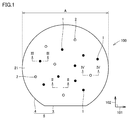
- FIG. 1 is a schematic plan view showing the configuration of the silicon carbide epitaxial substrate according to the first embodiment.
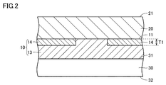
- FIG. 2 is a schematic cross-sectional view taken along the line II-II of FIG.
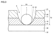
- FIG. 3 is a schematic cross-sectional view taken along the line III-III of FIG.
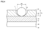
- FIG. 4 is a schematic cross-sectional view taken along the line IV-IV of FIG.
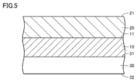
- FIG. 5 is a schematic cross-sectional view showing the configuration of the silicon carbide epitaxial substrate according to the second embodiment.
- FIG. 6 is a partial cross-sectional schematic diagram showing the configuration of a manufacturing apparatus for a silicon carbide epitaxial substrate.
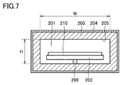
- FIG. 7 is a schematic cross-sectional view taken along the line VII-VII of FIG. FIG.
- FIG. 8 is a flowchart showing an outline of a method for manufacturing a silicon carbide epitaxial substrate according to the present embodiment.
- FIG. 9 is a schematic cross-sectional view showing a first step of the method for manufacturing a silicon carbide epitaxial substrate according to the present embodiment.
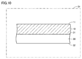
- FIG. 10 is a schematic cross-sectional view showing a second step of the method for manufacturing a silicon carbide epitaxial substrate according to the present embodiment.
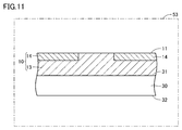
- FIG. 11 is a schematic cross-sectional view showing a third step of the method for manufacturing a silicon carbide epitaxial substrate according to the present embodiment.
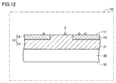
- FIG. 12 is a schematic cross-sectional view showing a fourth step of the method for manufacturing a silicon carbide epitaxial substrate according to the present embodiment.
- FIG. 9 is a schematic cross-sectional view showing a first step of the method for manufacturing a silicon carbide epitaxial substrate according to the present embodiment.
- FIG. 10 is a schematic cross-sectional view showing a second step of the method for manufacturing a
- FIG. 13 is a schematic cross-sectional view showing a fifth step of the method for manufacturing a silicon carbide epitaxial substrate according to the present embodiment.
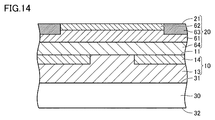
- FIG. 14 is a schematic cross-sectional view showing a first step of the method for manufacturing a silicon carbide semiconductor device according to the present embodiment.
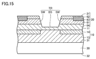
- FIG. 15 is a schematic cross-sectional view showing a second step of the method for manufacturing a silicon carbide semiconductor device according to the present embodiment.
- FIG. 16 is a schematic cross-sectional view showing a third step of the method for manufacturing a silicon carbide semiconductor device according to the present embodiment.
- FIG. 17 is a schematic cross-sectional view showing a fourth step of the method for manufacturing a silicon carbide semiconductor device according to the present embodiment.
- An object of the present disclosure is to provide a silicon carbide epitaxial substrate and a method for manufacturing a silicon carbide epitaxial substrate, which can suppress deterioration of the withstand voltage of a silicon carbide semiconductor device.
- a silicon carbide epitaxial substrate and a method for manufacturing a silicon carbide epitaxial substrate which can suppress deterioration of the withstand voltage of the silicon carbide semiconductor device.
- the silicon carbide epitaxial substrate 100 includes a silicon carbide substrate 30, a first silicon carbide epitaxial layer 10, and a second silicon carbide epitaxial layer 20.
- the first silicon carbide epitaxial layer 10 is on the silicon carbide substrate 30.
- the second silicon carbide epitaxial layer 20 is on the first silicon carbide epitaxial layer 10.
- the first surface density is used.
- the value obtained by dividing the surface density by the second surface density is greater than 0.5 and less than 1.
- the maximum diameter of each of the first particle 1 and the second particle 2 is 2 ⁇ m or more and 50 ⁇ m or less.
- the second surface density may be less than 10 cm-2.
- the first silicon carbide epitaxial layer 10 has a first region 13 having a first conductive type and a second region different from the first conductive type. It may include a second region 14 having a conductive type and in contact with the first region 13.
- the thickness of the second region 14 is the thickness of the second region 14 in the direction perpendicular to the interface between the first silicon carbide epitaxial layer 10 and the second silicon carbide epitaxial layer 20. It may be 1 ⁇ m or less.
- the first silicon carbide epitaxial layer 10 may have a first conductive type.
- the second silicon carbide epitaxial layer 20 may have a second conductive type different from the first conductive type.
- the method for manufacturing the silicon carbide epitaxial substrate 100 includes the following steps.
- the first silicon carbide epitaxial layer 10 is formed on the silicon carbide substrate 30 at the first temperature.
- the silicon carbide substrate 30 on which the first silicon carbide epitaxial layer 10 is formed is taken out from the first reaction chamber 51.
- a silicon carbide substrate 30 on which the first silicon carbide epitaxial layer 10 is formed is arranged in the second reaction chamber 52.
- the silicon carbide substrate 30 on which the first silicon carbide epitaxial layer 10 is formed is heated at the second temperature while flowing gas.
- the second silicon carbide epitaxial layer 20 is formed on the first silicon carbide epitaxial layer 10.
- the second temperature is lower than the first temperature.
- the second temperature may be 1500 ° C. or lower.
- the gas flow velocity is 15 cm / sec or more and 200 cm / sec or less under the conditions that the temperature is 300 K and the pressure is 1 atm. May be.
- the first reaction chamber 51 may be the same as the second reaction chamber 52.
- the first reaction chamber 51 may be different from the second reaction chamber 52.
- FIG. 1 is a schematic plan view showing the configuration of the silicon carbide epitaxial substrate according to the first embodiment.
- FIG. 2 is a schematic cross-sectional view taken along the line II-II of FIG.
- the silicon carbide epitaxial substrate 100 includes a silicon carbide substrate 30, a first silicon carbide epitaxial layer 10, and a second silicon carbide epitaxial layer 20. ing.
- the first silicon carbide epitaxial layer 10 is on the silicon carbide substrate 30.
- the second silicon carbide epitaxial layer 20 is on the first silicon carbide epitaxial layer 10.
- the first silicon carbide epitaxial layer 10 is located between the silicon carbide substrate 30 and the second silicon carbide epitaxial layer 20.
- the second silicon carbide epitaxial layer 20 constitutes the surface (first main surface 21) of the silicon carbide epitaxial substrate 100.
- the first main surface 21 has an outer peripheral edge 5 when viewed in a direction perpendicular to the first main surface 21.
- the outer peripheral edge 5 has, for example, an orientation flat 3 and an arcuate portion 4.
- the orientation flat 3 extends along the first direction 101.
- the orientation flat 3 is linear when viewed in a direction perpendicular to the first main surface 21.
- the arcuate portion 4 is connected to the orientation flat 3.
- the arcuate portion 4 has an arcuate shape when viewed in a direction perpendicular to the first main surface 21.
- the first main surface 21 when viewed in a direction perpendicular to the first main surface 21, the first main surface 21 extends along each of the first direction 101 and the second direction 102.
- the first direction 101 is a direction perpendicular to the second direction 102.
- the first direction 101 is, for example, the ⁇ 11-20> direction.
- the first direction 101 may be, for example, the [11-20] direction.
- the first direction 101 may be a direction in which the ⁇ 11-20> direction is projected onto the first main surface 21. From another point of view, the first direction 101 may be a direction including, for example, a ⁇ 11-20> direction component.
- the second direction 102 is, for example, the ⁇ 1-100> direction.
- the second direction 102 may be, for example, the [1-100] direction.
- the second direction 102 may be, for example, a direction in which the ⁇ 1-100> direction is projected onto the first main surface 21. From another point of view, the second direction 102 may be a direction containing, for example, a ⁇ 1-100> direction component.
- the first main surface 21 may be a surface inclined with respect to the ⁇ 0001 ⁇ surface.
- the inclination angle (off angle) with respect to the ⁇ 0001 ⁇ surface is, for example, 2 ° or more and 6 ° or less.
- the inclination direction (off direction) of the first main surface 21 is, for example, the ⁇ 11-20> direction.
- the maximum diameter A (diameter) of the first main surface 21 is not particularly limited, but is, for example, 100 mm (4 inches).
- the maximum diameter A may be 125 mm (5 inches) or more, or 150 mm (6 inches) or more.
- the upper limit of the maximum diameter A is not particularly limited.
- the maximum diameter A may be, for example, 200 (8 inches) mm or less.
- the maximum diameter A is the longest linear distance between two different points on the outer peripheral edge 5.
- 2 inches means 50 mm or 50.8 mm (2 inches x 25.4 mm / inch).
- 4 inches means 100 mm or 101.6 mm (4 inches x 25.4 mm / inch).
- 5 inches means 125 mm or 127.0 mm (5 inches x 25.4 mm / inch).
- 6 inches means 150 mm or 152.4 mm (6 inches x 25.4 mm / inch).
- 8 inches means 200 mm or 203.2 mm (8 inches x 25.4 mm / inch).
- the silicon carbide substrate 30 has a third main surface 31 and a second main surface 32.
- the second main surface 32 is a surface opposite to the third main surface 31.
- the second main surface 32 constitutes the back surface of the silicon carbide epitaxial substrate 100.
- the third main surface 31 is in contact with the first silicon carbide epitaxial layer 10.
- the polytype of silicon carbide constituting the silicon carbide substrate 30 is, for example, 4H.
- the polytype of silicon carbide constituting the first silicon carbide epitaxial layer 10 is, for example, 4H.
- the polytype of silicon carbide constituting the second silicon carbide epitaxial layer 20 is, for example, 4H.
- the silicon carbide substrate 30 contains n-type impurities such as nitrogen (N).
- the conductive type of the silicon carbide substrate 30 is, for example, an n-type (first conductive type).
- the thickness of the silicon carbide substrate 30 is, for example, 350 ⁇ m or more and 500 ⁇ m or less.
- the second silicon carbide epitaxial layer 20 contains n-type impurities such as nitrogen.
- the conductive type of the second silicon carbide epitaxial layer 20 is, for example, n type.
- the concentration of the n-type impurities contained in the second silicon carbide epitaxial layer 20 may be lower than the concentration of the n-type impurities contained in the silicon carbide substrate 30.
- the first silicon carbide epitaxial layer 10 has a first region 13 and a second region 14.
- the first region 13 has, for example, an n-type (first conductive type).
- the first region 13 contains n-type impurities such as nitrogen.
- the concentration of the n-type impurities contained in the first region 13 may be lower than the concentration of the n-type impurities contained in the silicon carbide substrate 30.
- the second region 14 has a p-type (second conductive type) different from the n-type (first conductive type).
- the second region 14 contains p-type impurities such as aluminum.
- the concentration of the p-type impurity contained in the second region 14 may be higher than the concentration of the n-type impurity contained in the first region 13.
- the first region 13 is provided on the silicon carbide substrate 30.
- the first region 13 is in contact with each of the silicon carbide substrate 30 and the second silicon carbide epitaxial layer 20.
- the first region 13 constitutes a part of the boundary surface 11 between the first silicon carbide epitaxial layer 10 and the second silicon carbide epitaxial layer 20.
- the first region 13 is in contact with the second region 14.
- the second region 14 is in contact with the second silicon carbide epitaxial layer 20.
- the second region 14 is separated from the silicon carbide substrate 30.
- the second region 14 constitutes a part of the boundary surface 11 between the first silicon carbide epitaxial layer 10 and the second silicon carbide epitaxial layer 20.
- the thickness of the second region 14 (first thickness T1) is, for example, 1 ⁇ m or less in the direction perpendicular to the boundary surface 11 between the first silicon carbide epitaxial layer 10 and the second silicon carbide epitaxial layer 20.
- the first thickness T1 may be 0.8 ⁇ m or less, or may be 0.5 ⁇ m or less.
- the lower limit of the first thickness T1 is not particularly limited, but may be, for example, 0.1 ⁇ m or more.
- FIG. 3 is a schematic cross-sectional view taken along the line III-III of FIG.
- the silicon carbide epitaxial substrate 100 has the first particle 1.
- the first particle 1 is in the first silicon carbide epitaxial layer 10.
- the bottom of the first particle 1 may be in contact with the silicon carbide substrate 30.
- the first particle 1 is surrounded by the first silicon carbide epitaxial layer 10 when viewed in a direction perpendicular to the second main surface 32.
- a part of the first particle 1 may be surrounded by the second silicon carbide epitaxial layer 20 when viewed in a direction perpendicular to the second main surface 32.
- a first recess 6 is provided on the first main surface 21 of the silicon carbide epitaxial substrate 100.
- the first particle 1 is inside the first recess 6.
- the first silicon carbide epitaxial layer 10 has a first side surface 12 connecting the boundary surface 11 and the third main surface 31.
- the second silicon carbide epitaxial layer 20 has a second side surface 22 connecting the boundary surface 11 and the first main surface 21.
- the second side surface 22 may be connected to the first side surface 12.
- the first recess 6 is composed of, for example, a first side surface 12, a second side surface 22, and a third main surface 31.
- the first side surface 12 surrounds the first particle 1 when viewed in a direction perpendicular to the second main surface 32. A part of the first side surface 12 may be in contact with the first particle 1 or may be separated from the first particle 1.
- the second side surface 22 surrounds the first particle 1 when viewed in a direction perpendicular to the second main surface 32. The second side surface 22 may be separated from the first particle 1. A part of the first particle 1 may protrude from the first recess 6.
- the maximum diameter (first maximum diameter D1) of the first particle 1 viewed in the direction perpendicular to the second main surface 32 is the total thickness (first) of the first silicon carbide epitaxial layer 10 and the second silicon carbide epitaxial layer 20. 2 Thickness may be larger than T2).
- the depth of the first recess 6 is the same as that of the second thickness T2.
- the maximum diameter of the first particle 1 (first maximum diameter D1) may be larger or smaller than the depth of the first recess 6.
- the first maximum diameter D1 is 2 ⁇ m or more and 50 ⁇ m or less.
- the upper limit of the first maximum diameter D1 may be 45 ⁇ m or less, or may be 40 ⁇ m or less.
- the lower limit of the first maximum diameter D1 may be 4 ⁇ m or more, or 6 ⁇ m or more.
- FIG. 4 is a schematic cross-sectional view taken along the line IV-IV of FIG.
- the silicon carbide epitaxial substrate 100 has the second particle 2.
- the second particle 2 is in the second silicon carbide epitaxial layer 20.
- the bottom of the second particle 2 may be in contact with the first silicon carbide epitaxial layer 10.
- the second particle 2 is separated from the silicon carbide substrate 30.
- the second particle 2 is surrounded by the second silicon carbide epitaxial layer 20 when viewed in a direction perpendicular to the second main surface 32.
- the first silicon carbide epitaxial layer 10 is located between the second particles 2 and the silicon carbide substrate 30. From another point of view, the second particle 2 is located closer to the first main surface 21 than the boundary surface 11 in the direction perpendicular to the second main surface 32.
- a second recess 7 is provided on the first main surface 21 of the silicon carbide epitaxial substrate 100.
- the second particle 2 is inside the second recess 7.
- the second silicon carbide epitaxial layer 20 has a third side surface 23 connecting the boundary surface 11 and the first main surface 21.
- the second recess 7 is composed of, for example, a third side surface 23 and a boundary surface 11.
- the third side surface 23 surrounds the second particle 2 when viewed in a direction perpendicular to the second main surface 32. A part of the third side surface 23 may be in contact with the second particle 2 or may be separated from the second particle 2. A part of the second particle 2 may protrude from the second recess 7.
- the maximum diameter (second maximum diameter D2) of the second particles 2 viewed in the direction perpendicular to the second main surface 32 may be larger than the thickness of the second silicon carbide epitaxial layer 20 (third thickness T3).
- the depth of the second recess 7 is the same as that of the third thickness T3.
- the maximum diameter of the second particle 2 (second maximum diameter D2) may be larger or smaller than the depth of the second recess 7.
- the second maximum diameter D2 is 2 ⁇ m or more and 50 ⁇ m or less.
- the upper limit of the second maximum diameter D2 may be 45 ⁇ m or less, or may be 40 ⁇ m or less.
- the lower limit of the second maximum diameter D2 may be 4 ⁇ m or more, or 6 ⁇ m or more.
- Each of the first particle 1 and the second particle 2 is, for example, a downfall.
- the deposits deposited on the inner wall of the CVD apparatus have fallen onto the silicon carbide substrate 30.
- the downfall is, for example, polycrystalline silicon carbide, carbon or tantalum carbide (TaC) and the like.
- the surface density of the first particles 1 in the first silicon carbide epitaxial layer 10 is set to the first surface density
- the surface density of the second particles 2 in the second silicon carbide epitaxial layer 20 is set.
- the surface density is the second surface density
- the value (density ratio) obtained by dividing the first surface density by the second surface density is greater than 0.5 and less than 1.
- the lower limit of the density ratio is not particularly limited, but may be 0.6 or more, or may be 0.7 or more.
- the second surface density is, for example, less than 10 cm-2.
- the second surface density may be, for example, less than 5 cm-2 or less than 2 cm- 2 .
- the lower limit of the second surface density is not particularly limited, but may be , for example, 0.01 pieces cm-2 or more.
- the configuration of the silicon carbide epitaxial substrate 100 according to the second embodiment will be described.
- the first silicon carbide epitaxial layer 10 has a first conductive type
- the second silicon carbide epitaxial layer 20 has a second conductive type.
- the configuration is different from that of the silicon carbide epitaxial substrate 100 according to the first embodiment, and other configurations are the same as those of the silicon carbide epitaxial substrate 100 according to the first embodiment.
- FIG. 5 is a schematic cross-sectional view showing the configuration of the silicon carbide epitaxial substrate according to the second embodiment.
- the field of view of FIG. 5 corresponds to a schematic cross-sectional view taken along line II-II of FIG.
- the first silicon carbide epitaxial layer 10 has an n-type (first conductive type).
- the first silicon carbide epitaxial layer 10 contains n-type impurities such as nitrogen.
- the concentration of the n-type impurities contained in the first silicon carbide epitaxial layer 10 may be lower than the concentration of the n-type impurities contained in the silicon carbide substrate 30.
- the second silicon carbide epitaxial layer 20 has a p-type (second conductive type) different from the n-type (first conductive type).
- the second silicon carbide epitaxial layer 20 contains p-type impurities such as aluminum.
- the second silicon carbide epitaxial layer 20 is provided on the first silicon carbide epitaxial layer 10.
- the first particle 1 and the second particle 2 can be identified by observing the surface (first main surface 21) of the second silicon carbide epitaxial layer 20 using, for example, a defect inspection apparatus equipped with a confocal differential interference microscope. can.
- a defect inspection apparatus equipped with a confocal differential interference microscope for example, a WASAVI series "SICA 6X” manufactured by Lasertec Co., Ltd. can be used.
- the magnification of the objective lens is, for example, 10 times.
- the threshold of the detection sensitivity of the defect inspection device is determined by using a standard sample.
- the downfall defect is defined in advance in consideration of the typical planar shape, dimensions, etc. of the downfall defect. Based on the observed image, the location and number of defects that meet the definition of downfall defects are identified.
- a confocal differential interference contrast microscope image of the entire first main surface 21 is taken.
- both the first particle 1 and the second particle 2 are observed.
- the total number of the first particle 1 and the second particle 2 is obtained.
- the second silicon carbide epitaxial layer 20 is removed. Specifically, the second silicon carbide epitaxial layer 20 is polished on the first main surface 21. In this case, the second particle 2 is also removed by polishing together with the second silicon carbide epitaxial layer 20. As a result, the first silicon carbide epitaxial layer 10 and the silicon carbide substrate 30 remain. The polishing may remove the first particles 1 in the first silicon carbide epitaxial layer 10.
- a confocal differential interference contrast microscope image of the entire boundary surface 11 is taken.
- the remaining first particle 1 and the first recess 6 in which the first particle 1 was present are observed.
- the total number of the remaining first particle 1 and the first recess 6 in which the first particle 1 was present is specified.
- the total number of the remaining first particles 1 and the first recess 6 in which the first particles 1 were present is estimated to be the number of the first particles 1 that were present before polishing.
- the value obtained by subtracting the number of the first particles 1 from the total number of the first particles 1 and the second particles 2 is the number of the second particles 2.
- the value obtained by dividing the number of each of the first particle 1 and the second particle 2 by the measured area is taken as the surface density.
- the measurement area is the first main surface 21 excluding the outer peripheral area within 3 mm from the outer peripheral edge 5.
- FIG. 6 is a partial cross-sectional schematic diagram showing the configuration of a manufacturing apparatus for a silicon carbide epitaxial substrate.
- the silicon carbide epitaxial substrate manufacturing apparatus 200 is, for example, a hot wall type horizontal CVD (Chemical Vapor Deposition) apparatus.
- the manufacturing apparatus 200 mainly includes a reaction chamber 201, a gas supply unit 235, a control unit 245, a heating element 203, a quartz tube 204, and an induction heating coil (not shown).
- the heating element 203 has, for example, a cylindrical shape, and forms a reaction chamber 201 inside.
- the heating element 203 is made of graphite, for example.
- the induction heating coil is wound, for example, along the outer peripheral surface of the quartz tube 204.
- the induction heating coil is configured to be able to supply an alternating current by an external power source (not shown). As a result, the heating element 203 is induced and heated. As a result, the reaction chamber 201 is heated by the heating element 203.
- the reaction chamber 201 is a space formed by being surrounded by the inner wall surface 205 of the heating element 203.
- a silicon carbide substrate 30 is arranged in the reaction chamber 201.
- the reaction chamber 201 is configured to be able to heat the silicon carbide substrate 30.
- the reaction chamber 201 is provided with a susceptor 210 for holding the silicon carbide substrate 30.
- the susceptor 210 is arranged on the stage 202.
- the stage 202 is configured to be rotatable by a rotation shaft 209. As the stage 202 rotates, the susceptor 210 rotates.
- the manufacturing apparatus 200 further has a gas introduction port 207 and a gas exhaust port 208.
- the gas exhaust port 208 is connected to an exhaust pump (not shown). Arrows in FIG. 6 indicate gas flow.
- the gas is introduced into the reaction chamber 201 from the gas introduction port 207 and exhausted from the gas exhaust port 208.
- the pressure in the reaction chamber 201 is adjusted by the balance between the amount of gas supplied and the amount of gas exhausted.
- the gas supply unit 235 is configured to be able to supply a mixed gas containing, for example, silane, propane, ammonia, and hydrogen to the reaction chamber 201.
- the gas supply unit 235 may include a first gas supply unit 231, a second gas supply unit 232, a third gas supply unit 233, and a carrier gas supply unit 234.
- the first gas supply unit 231 is configured to be able to supply the first gas.
- the first gas supply unit 231 is, for example, a gas cylinder filled with the first gas.
- the first gas is, for example, propane (C 3 H 8 ) gas.
- the first gas may be, for example, methane (CH 4 ) gas, ethane (C 2 H 6 ) gas, acetylene (C 2 H 2 ) gas, or the like.
- the second gas supply unit 232 is configured to be able to supply the second gas.
- the second gas supply unit 232 is, for example, a gas cylinder filled with the second gas.
- the second gas is, for example, a silane (SiH 4 ) gas.
- the second gas may be a mixed gas of silane gas and a gas other than silane.
- the third gas supply unit 233 is configured to be able to supply the third gas.
- the third gas supply unit 233 is, for example, a gas cylinder filled with the third gas.
- the third gas is a doping gas containing N (nitrogen atom). Ammonia gas is more easily pyrolyzed than nitrogen gas having a triple bond. By using ammonia gas, improvement of in-plane uniformity of carrier concentration can be expected.
- the carrier gas supply unit 234 is configured to be able to supply a carrier gas such as hydrogen.
- the carrier gas supply unit 234 is, for example, a gas cylinder filled with hydrogen.
- the control unit 245 is configured to be able to control the flow rate of the mixed gas supplied from the gas supply unit 235 to the reaction chamber 201.
- the control unit 245 may include a first gas flow rate control unit 241, a second gas flow rate control unit 242, a third gas flow rate control unit 243, and a carrier gas flow rate control unit 244. ..
- Each control unit may be, for example, an MFC (Mass Flow Controller).
- the control unit 245 is arranged between the gas supply unit 235 and the gas introduction port 207. In other words, the control unit 245 is arranged in the flow path connecting the gas supply unit 235 and the gas introduction port 207.
- FIG. 7 is a schematic cross-sectional view taken along the line VII-VII of FIG.
- the region surrounded by the inner wall surface 205 of the heating element 203 is, for example, substantially rectangular.
- the width W of the region surrounded by the inner wall surface 205 of the heating element 203 in the radial direction of the silicon carbide substrate 30 is the inner wall surface 205 of the heating element 203 in the direction perpendicular to the radial direction of the silicon carbide substrate 30. It may be larger than the height H of the area surrounded by.
- the cross-sectional area of the reaction chamber 201 is, for example, 50 cm 2 .
- the lower limit of the cross-sectional area of the reaction chamber 201 is not particularly limited, but may be , for example, 30 cm 2 or more, or 40 cm 2 or more.
- the upper limit of the cross-sectional area of the reaction chamber 201 is not particularly limited, but may be , for example, 70 cm 2 or less, or 60 cm 2 or less.
- the cross-sectional area of the reaction chamber 201 is the area (width W ⁇ height H) of the region surrounded by the inner wall surface 205 of the heating element 203 in the cross section perpendicular to the traveling direction of the reaction gas (FIG. 7). reference).
- FIG. 8 is a flowchart showing an outline of a method for manufacturing a silicon carbide epitaxial substrate according to the present embodiment.
- the method for manufacturing the silicon carbide epitaxial substrate 100 according to the present embodiment includes a step (S10) of forming the first silicon carbide epitaxial layer in the first reaction chamber and silicon carbide from the first reaction chamber.
- the silicon carbide substrate 30 is prepared.
- the sublimation method produces a polytype 4H silicon carbide single crystal.
- the silicon carbide substrate 30 is prepared by slicing the silicon carbide single crystal with, for example, a wire saw.
- the silicon carbide substrate 30 contains n-type impurities such as nitrogen.
- the conductive type of the silicon carbide substrate 30 is, for example, n type.
- the step (S10) of forming the first silicon carbide epitaxial layer in the first reaction chamber is carried out.
- the first reaction chamber 51 is, for example, the reaction chamber 201 of the manufacturing apparatus shown in FIG.
- the silicon carbide substrate 30 is placed on the susceptor 210 (see FIG. 6).
- the silicon carbide substrate 30 has a third main surface 31 and a second main surface 32 on the opposite side of the third main surface 31.
- the third main surface 31 is, for example, a surface inclined in the off direction by an off angle with respect to the ⁇ 0001 ⁇ surface.
- the off angle is, for example, 2 ° or more and 6 ° or less.
- the off direction is, for example, the ⁇ 11-20> direction.
- the maximum diameter of the third main surface 31 is, for example, 150 mm.
- the pressure in the first reaction chamber 51 is reduced from the atmospheric pressure to about 1 ⁇ 10 -6 Pa.
- the temperature rise of the silicon carbide substrate 30 is started.
- hydrogen (H 2 ) gas which is a carrier gas, is introduced into the first reaction chamber 51 from the carrier gas supply unit 234.
- the flow rate of hydrogen gas is adjusted by the carrier gas flow rate control unit 244.
- the raw material gas, the dopant gas and the carrier gas are supplied to the first reaction chamber 51. Specifically, by supplying a mixed gas containing silane, ammonia, hydrogen, and propane to the reaction chamber 201, each gas is thermally decomposed. As a result, in the first reaction chamber 51, the first silicon carbide epitaxial layer 10 is formed on the silicon carbide substrate 30 at 1600 ° C. (first temperature) (see FIG. 10).
- the step (S20) of taking out the silicon carbide substrate from the first reaction chamber is carried out. Specifically, the silicon carbide substrate 30 on which the first silicon carbide epitaxial layer 10 is formed is taken out from the first reaction chamber 51. Next, the silicon carbide substrate 30 on which the first silicon carbide epitaxial layer 10 is formed is arranged inside the ion implantation device 53.
- a p-type region (second region 14) is formed in the first silicon carbide epitaxial layer 10.
- an injection mask (not shown) having an opening is formed on the first silicon carbide epitaxial layer 10.
- Impurities such as aluminum are ion-implanted into the first silicon carbide epitaxial layer 10 using the injection mask.
- a p-type region (second region 14) is formed in the first silicon carbide epitaxial layer 10 (see FIG. 11).
- the region in which the p-type region (second region 14) is not formed becomes the n-type region (first region 13).
- the first silicon carbide epitaxial layer 10 is composed of a first region 13 and a second region 14.
- the silicon carbide substrate 30 on which the first silicon carbide epitaxial layer 10 is formed is arranged in the second reaction chamber 52.
- the second reaction chamber 52 is, for example, the reaction chamber 201 of the manufacturing apparatus shown in FIG. That is, the first reaction chamber 51 may be the same as the second reaction chamber 52. Alternatively, the first reaction chamber 51 may be different from the second reaction chamber 52.
- the silicon carbide substrate 30 may be arranged in the reaction chamber of the CVD apparatus on which the first silicon carbide epitaxial layer 10 is formed, or the CVD apparatus on which the first silicon carbide epitaxial layer 10 is formed. It may be arranged in a reaction chamber of a different CVD device.
- a step (S40) of cleaning the surface of the first silicon carbide epitaxial layer in the second reaction chamber is carried out.
- the silicon carbide substrate 30 on which the first silicon carbide epitaxial layer 10 was formed was arranged in the second reaction chamber 52, the downfall (second particle 2) existing in the second reaction chamber 52 was first carbonized. It may adhere to the surface of the silicon epitaxial layer 10 (see FIG. 12). In order to remove such downfall, the surface (boundary surface 11) of the first silicon carbide epitaxial layer 10 is cleaned.
- the silicon carbide substrate 30 on which the first silicon carbide epitaxial layer 10 is formed is heated at the second temperature while flowing gas.
- the cleaning temperature is set low in order to suppress sublimation of the p-type region (second region 14) formed in the first silicon carbide epitaxial layer 10.
- the second temperature is lower than the first temperature.
- the second temperature is, for example, 1500 ° C. or lower.
- the second temperature may be, for example, 1300 ° C. or lower, 1099 ° C. or lower, or 999 ° C. or lower.
- sublimation of the p-type region (second region 14) can be further suppressed.
- the gas flow velocity is set high.
- the gas flow velocity is a value obtained by dividing the flow rate of the gas introduced into the second reaction chamber 52 by the cross-sectional area of the second reaction chamber 52 in the cross section perpendicular to the direction in which the gas flows.
- the flow rate of the gas is, for example, 15 cm / sec or more under standard conditions of room temperature (300 K) and atmospheric pressure (1 atm).
- the flow rate of the gas may be 10 cm / sec or more, or 30 cm / sec or more.
- the upper limit of the gas flow velocity is, for example, 200 cm / sec or less.
- the upper limit of the flow rate of the gas is not particularly limited, but may be, for example, 150 cm / sec or less, or may be 100 cm / sec or less, for example. From the viewpoint of suppressing the damage of the member and the viewpoint of suppressing the generation of the dust source, it is preferable that the flow velocity of the gas is not too high.
- the flow velocity of the gas increases when the temperature rises or the pressure drops with respect to the standard conditions of room temperature (300 K) and atmospheric pressure (1 atm).
- the gas is, for example, hydrogen gas.
- the gas may be, for example, a noble gas.
- the gas may be, for example, argon gas, helium gas, nitrogen gas, or the like. From another point of view, the gas preferably contains any of argon, helium, hydrogen, and nitrogen.
- the step (S50) of forming the second silicon carbide epitaxial layer in the second reaction chamber is carried out.
- the second silicon carbide epitaxial layer 20 is formed on the first silicon carbide epitaxial layer 10.
- the raw material gas, the dopant gas and the carrier gas are supplied to the second reaction chamber 52.
- a mixed gas containing silane, ammonia, hydrogen, and propane supplied to the reaction chamber 201.
- each gas is thermally decomposed.
- the second silicon carbide epitaxial layer 20 is formed on the first silicon carbide epitaxial layer 10 at a third temperature higher than the second temperature.
- the third temperature is, for example, 1600 ° C.
- the silicon carbide epitaxial substrate 100 (FIG. 2) according to the present embodiment is manufactured.
- the silicon carbide semiconductor device is, for example, a MOSFET (Metal Oxide Semiconductor Field Effect Transistor).
- the silicon carbide epitaxial substrate 100 (see FIG. 2) is prepared.
- the body region 61 is formed by ion-implanting impurities such as aluminum into the second silicon carbide epitaxial layer 20.
- the source region 62 is formed by ion-implanting impurities such as phosphorus into the body region 61 at a depth shallower than that of the body region 61.
- the contact region 63 is formed by ion-implanting an impurity such as aluminum into the source region 62 (see FIG. 14).
- heat treatment is performed to activate the ion-implanted impurities.
- the temperature of the activation annealing is preferably 1500 ° C. or higher and 1900 ° C. or lower, for example, about 1700 ° C.
- the activation annealing time is, for example, about 30 minutes.
- the atmosphere of the activated annealing is preferably an inert gas atmosphere, for example, an Ar atmosphere.
- a trench TR is formed on the first main surface 21 of the silicon carbide substrate 30 epitaxial substrate.
- a mask layer (not shown) having an opening is formed on the first main surface 21.
- the source region 62, the body region 61, and a part of the drift region 64 are removed by etching.
- the etching method for example, reactive ion etching, particularly inductively coupled plasma reactive ion etching can be used.
- inductively coupled plasma reactive ion etching using SF 6 or a mixed gas of SF 6 and O 2 can be used as the reaction gas.
- Thermal etching can be performed, for example, by heating in an atmosphere containing a reactive gas having at least one halogen atom. At least one or more halogen atoms contain at least one of a chlorine (Cl) atom and a fluorine (F) atom.
- This atmosphere is, for example, Cl 2 , BCl 3 , SF 6 , or CF 4 .
- a mixed gas of chlorine gas and oxygen gas is used as a reaction gas, and the heat treatment temperature is set to, for example, 700 ° C. or higher and 1000 ° C. or lower, and thermal etching is performed.
- a trench TR is formed on the first main surface 21 of the silicon carbide epitaxial substrate 100 by the above thermal etching.
- the trench TR is formed by a side SW that penetrates the source region 62 and the body region 61 and reaches the drift region 64, and a bottom BS that is located on the drift region 64.
- the side SW of the trench TR is inclined with respect to the bottom BS, and the angle formed by the bottom BS and the side SW is, for example, 110 ° or more and 130 ° or less.
- the gate insulating film 71 is formed.
- the gate insulating film 71 is formed by thermally oxidizing the silicon carbide epitaxial substrate 100 on which the trench TR is formed. Specifically, the silicon carbide epitaxial substrate 100 on which the trench TR is formed is heated at, for example, about 1300 ° C. in an atmosphere containing oxygen to form the gate insulating film 71.
- the gate insulating film 71 is formed so as to cover the side SW, the bottom BS, and the first main surface 21.
- the gate electrode 72 is formed. Inside the trench TR, a gate electrode 72 in contact with the gate insulating film 71 is formed.
- the gate electrode 72 is arranged inside the trench TR, and is formed so as to face each of the side SW and the bottom BS of the trench TR via the gate insulating film 71.
- the gate electrode 72 is formed by, for example, an LPCVD (Low Pressure Chemical Vapor Deposition) method.
- the interlayer insulating film 73 is formed. Specifically, the interlayer insulating film 73 is formed so as to cover the gate electrode 72 and contact the gate insulating film 71. Preferably, the interlayer insulating film 73 is formed by a deposition method, and more preferably by a chemical vapor deposition method.
- the interlayer insulating film 73 is a material containing, for example, silicon dioxide.
- the source electrode 80 is formed. Specifically, etching is performed so that an opening is formed in the interlayer insulating film 73 and the gate insulating film 71, and each of the source region 62 and the contact region 63 is exposed from the interlayer insulating film 73 by the opening. See FIG. 16).
- an electrode layer 81 in contact with each of the source region 62 and the contact region 63 is formed on the first main surface 21.
- the electrode layer 81 is made of a material containing, for example, Ti, Al and Si.
- alloying annealing is performed. Specifically, the electrode layer 81 in contact with each of the source region 62 and the contact region 63 is held at a temperature of, for example, 900 ° C.
- the electrode layer 81 is alloyed by reacting with the silicon contained in the silicon carbide substrate 30 to silicide. As a result, the electrode layer 81 is ohmic-bonded to the source region 62.
- the source wiring 82 is formed.
- the source wiring 82 is formed on the electrode layer 81 and the interlayer insulating film 73.
- the source wiring 82 includes, for example, aluminum.
- the source electrode 80 including the electrode layer 81 and the source wiring 82 is formed.
- the drain electrode 90 is formed so as to be in contact with the second main surface 32 of the silicon carbide substrate 30. As described above, the silicon carbide semiconductor device (FIG. 17) according to the present embodiment is obtained.
- a CVD device When forming the silicon carbide epitaxial layer on the silicon carbide substrate 30, a CVD device is generally used.
- the silicon carbide substrate 30 When the silicon carbide substrate 30 is arranged in the reaction chamber of the CVD apparatus, the deposits accumulated on the inner wall of the reaction chamber of the CVD apparatus may fall onto the silicon carbide substrate 30. This falling object is a particle called a downfall.
- the material of the particles is, for example, polycrystalline silicon carbide, carbon or tantalum carbide (TaC) and the like.
- the surface of the silicon carbide substrate 30 may be etched with hydrogen or the like.
- the downfall is removed and the surface layer of the silicon carbide substrate 30 is removed by about 1 ⁇ m. Therefore, when hydrogen etching is performed after forming the first silicon carbide epitaxial layer 10 on the silicon carbide substrate 30, the thickness of the first silicon carbide epitaxial layer 10 becomes small.
- the surface layer of the first silicon carbide epitaxial layer 10 has a p-type region (second region 14) having a small thickness, the p-type region (second region 14) disappears when hydrogen etching is performed. Resulting in. Therefore, hydrogen etching cannot be performed after the first silicon carbide epitaxial layer 10 is formed. As a result, it was not possible to reduce particles such as downfall.
- the inventors have obtained the following findings as a result of diligent studies on measures for removing particles such as downfall without eliminating the p-type region.
- a method of cleaning the surface of the first silicon carbide epitaxial layer 10 while suppressing etching of the first silicon carbide epitaxial layer 10. I found. Specifically, in the second reaction chamber 52, the silicon carbide substrate 30 on which the first silicon carbide epitaxial layer 10 was formed was heated at a second temperature lower than the first temperature while flowing a gas. As a result, particles such as downfall on the first silicon carbide epitaxial layer 10 can be removed without substantially etching the first silicon carbide epitaxial layer 10.
- a channel region of the silicon carbide semiconductor device is usually formed.
- the crystallinity of silicon may deteriorate.
- the withstand voltage of the silicon carbide semiconductor device may deteriorate.
- the surface density (first surface density) of the first particles 1 is reduced by hydrogen-etching the surface of the silicon carbide substrate 30. Can be done.
- the surface density of the second particles 2 cannot be hydrogen-etched because the surface of the first silicon carbide epitaxial layer 10 cannot be hydrogen-etched. (Second surface density) could not be reduced. Therefore, the value obtained by dividing the first surface density by the second surface density could not be made larger than 0.5.
- the surface density of the first particles 1 in the first silicon carbide epitaxial layer 10 is set to the first surface density
- the second particles 2 in the second silicon carbide epitaxial layer 20 are set.
- the surface density of is the second surface density
- the value obtained by dividing the first surface density by the second surface density is greater than 0.5 and less than 1.
- the surface density of the second particles 2 in the second silicon carbide epitaxial layer 20 can be reduced.
- the silicon carbide epitaxial substrates according to Samples 1 to 8 were prepared.
- the diameter of the silicon carbide epitaxial substrate according to Samples 1 to 8 was 150 mm (6 inches).
- the silicon carbide epitaxial substrates according to Samples 1 to 4 are comparative examples.
- the silicon carbide epitaxial substrates according to Samples 5 to 8 are examples.
- the step (S40) of cleaning the surface of the first silicon carbide epitaxial layer was not carried out.
- a step (S40) of cleaning the surface of the first silicon carbide epitaxial layer was carried out.
- the calculated value of the gas flow velocity in the step (S40) of cleaning the surface of the first silicon carbide epitaxial layer was assumed to correspond to 33.3 cm / sec under standard conditions.
- each of the first particle and the second particle was identified using the WASAVI series "SICA 6X” manufactured by Lasertec Co., Ltd.
- the numbers of the first particles and the second particles were counted on the first main surface 21 excluding the outer peripheral region within 3 mm from the outer peripheral edge 5.
- the area of the first main surface 21 excluding the outer peripheral region within 3 mm from the outer peripheral edge 5 is 161 cm 2 .
- the value obtained by dividing the number of the first particles by the number of the second particles is the value obtained by dividing the first surface density by the second surface density.
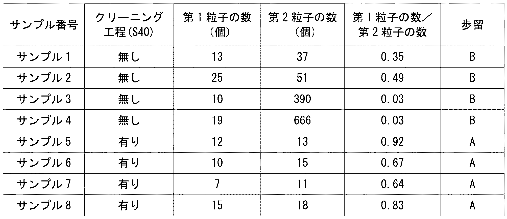
- the yield of MOSFETs for which silicon carbide semiconductor devices (MOSFETs) were prepared using the silicon carbide epitaxial substrates according to Samples 1 to 8 was determined. The yield of the MOSFET was performed based on the criterion of whether or not the withstand voltage of the MOSFET reached the reference value. When the yield was 82% or more, it was evaluated as "A", and when the yield was less than 82%, it was evaluated as "B".
- Table 1 shows the number of first particles, the number of second particles, the value obtained by dividing the number of first particles by the number of second particles, and the yield of MOSFET in the silicon carbide epitaxial substrate 100 according to Samples 1 to 8. Shows.
- Table 1 when the value obtained by dividing the number of the first particles by the number of the second particles is larger than 0.5, the evaluation result of the withstand voltage yield of the silicon carbide semiconductor device becomes "A". It was confirmed that it would be. That is, it was confirmed that deterioration of the withstand voltage of the silicon carbide semiconductor device can be suppressed by making the value obtained by dividing the number of the first particles by the number of the second particles larger than 0.5.
Landscapes
- Chemical & Material Sciences (AREA)
- Engineering & Computer Science (AREA)
- Materials Engineering (AREA)
- Metallurgy (AREA)
- Organic Chemistry (AREA)
- Chemical Kinetics & Catalysis (AREA)
- General Chemical & Material Sciences (AREA)
- Crystallography & Structural Chemistry (AREA)
- Inorganic Chemistry (AREA)
- Mechanical Engineering (AREA)
- Crystals, And After-Treatments Of Crystals (AREA)
Abstract
Description
本開示の目的は、炭化珪素半導体装置の耐圧が劣化することを抑制可能な炭化珪素エピタキシャル基板および炭化珪素エピタキシャル基板の製造方法を提供することである。
[本開示の効果]
本開示によれば、炭化珪素半導体装置の耐圧が劣化することを抑制可能な炭化珪素エピタキシャル基板および炭化珪素エピタキシャル基板の製造方法を提供することができる。
まず本開示の実施形態の概要について説明する。本明細書の結晶学的記載においては、個別方位を[]、集合方位を<>、個別面を()、集合面を{}でそれぞれ示す。結晶学上の指数が負であることは、通常、数字の上に”-”(バー)を付すことによって表現されるが、本明細書では数字の前に負の符号を付すことによって結晶学上の負の指数を表現する。
以下、本開示の実施形態の詳細について説明する。以下の説明では、同一または対応する要素には同一の符号を付し、それらについて同じ説明は繰り返さない。
まず、第1実施形態に係る炭化珪素エピタキシャル基板の構成について説明する。図1は、第1実施形態に係る炭化珪素エピタキシャル基板の構成を示す平面模式図である。図2は、図1のII-II線に沿った断面模式図である。
次に、第2実施形態に係る炭化珪素エピタキシャル基板100の構成について説明する。第2実施形態に係る炭化珪素エピタキシャル基板100の構成は、第1炭化珪素エピタキシャル層10は第1導電型を有しており、かつ、第2炭化珪素エピタキシャル層20は第2導電型を有している点において、第1実施形態に係る炭化珪素エピタキシャル基板100の構成と異なっており、その他の構成については、第1実施形態に係る炭化珪素エピタキシャル基板100と同様である。
次に、第1粒子1および第2粒子2の測定方法について説明する。
次に、炭化珪素エピタキシャル基板100の製造装置200の構成について説明する。
次に、本実施形態に係る炭化珪素エピタキシャル基板100の製造方法について説明する。
次に、炭化珪素半導体装置の製造方法について説明する。炭化珪素半導体装置は、たとえばMOSFET(Metal Oxide Semiconductor Field Effect Transistor)である。
まず、サンプル1~8に係る炭化珪素エピタキシャル基板を準備した。サンプル1~8に係る炭化珪素エピタキシャル基板の直径は、150mm(6インチ)とした。サンプル1~4に係る炭化珪素エピタキシャル基板は、比較例である。サンプル5~8に係る炭化珪素エピタキシャル基板は、実施例である。サンプル1~4に係る炭化珪素エピタキシャル基板の製造工程においては、第1炭化珪素エピタキシャル層の表面をクリーニングする工程(S40)が実施されなかった。サンプル5~8に係る炭化珪素エピタキシャル基板の製造工程においては、第1炭化珪素エピタキシャル層の表面をクリーニングする工程(S40)が実施された。第1炭化珪素エピタキシャル層の表面をクリーニングする工程(S40)におけるガスの流速の計算値は、標準条件において33.3cm/秒に相当するものとした。
次に、レーザーテック株式会社製のWASAVIシリーズ「SICA 6X」を用いて、第1粒子および第2粒子の各々を特定した。次に、外周縁5から3mm以内の外周領域を除いた第1主面21において、第1粒子および第2粒子の各々の数を数えた。なお、外周縁5から3mm以内の外周領域を除いた第1主面21の面積は、161cm2である。
Claims (10)
- 炭化珪素基板と、
前記炭化珪素基板上にある第1炭化珪素エピタキシャル層と、
前記第1炭化珪素エピタキシャル層上にある第2炭化珪素エピタキシャル層とを備え、
前記第1炭化珪素エピタキシャル層における第1粒子の面密度を第1面密度とし、かつ、前記第2炭化珪素エピタキシャル層における第2粒子の面密度を第2面密度とした場合、前記第1面密度を前記第2面密度で除した値は、0.5よりも大きく1未満であり、
前記第1粒子および前記第2粒子の各々の最大径は、2μm以上50μm以下である、炭化珪素エピタキシャル基板。 - 前記第2面密度は、10個cm-2未満である、請求項1に記載の炭化珪素エピタキシャル基板。
- 前記第1炭化珪素エピタキシャル層は、第1導電型を有する第1領域と、前記第1導電型とは異なる第2導電型を有しかつ前記第1領域に接する第2領域とを含む、請求項1または請求項2に記載の炭化珪素エピタキシャル基板。
- 前記第1炭化珪素エピタキシャル層と前記第2炭化珪素エピタキシャル層との境界面に対して垂直な方向において、前記第2領域の厚みは1μm以下である、請求項3に記載の炭化珪素エピタキシャル基板。
- 前記第1炭化珪素エピタキシャル層は、第1導電型を有しており、
前記第2炭化珪素エピタキシャル層は、前記第1導電型とは異なる第2導電型を有している、請求項1または請求項2に記載の炭化珪素エピタキシャル基板。 - 第1反応室において、第1温度で炭化珪素基板上に第1炭化珪素エピタキシャル層を形成する工程と、
前記第1反応室から前記第1炭化珪素エピタキシャル層が形成された前記炭化珪素基板を取り出す工程と、
第2反応室に前記第1炭化珪素エピタキシャル層が形成された前記炭化珪素基板を配置する工程と、
前記第2反応室において、ガスを流しながら、前記第1炭化珪素エピタキシャル層が形成された前記炭化珪素基板を第2温度で加熱する工程と、
前記第2反応室において、前記第1炭化珪素エピタキシャル層上に第2炭化珪素エピタキシャル層を形成する工程とを備え、
前記第2温度は、前記第1温度よりも低い、炭化珪素エピタキシャル基板の製造方法。 - 前記第2温度は、1500℃以下である、請求項6に記載の炭化珪素エピタキシャル基板の製造方法。
- 前記ガスの流速は、温度が300Kでありかつ圧力が1気圧である条件において15cm/秒以上200cm/秒以下である、請求項6または請求項7に記載の炭化珪素エピタキシャル基板の製造方法。
- 前記第1反応室は、前記第2反応室と同じである、請求項6から請求項8のいずれか1項に記載の炭化珪素エピタキシャル基板の製造方法。
- 前記第1反応室は、前記第2反応室と異なっている、請求項6から請求項8のいずれか1項に記載の炭化珪素エピタキシャル基板の製造方法。
Priority Applications (2)
| Application Number | Priority Date | Filing Date | Title |
|---|---|---|---|
| JP2022533731A JP7831290B2 (ja) | 2020-07-02 | 2021-05-20 | 炭化珪素エピタキシャル基板および炭化珪素エピタキシャル基板の製造方法 |
| US18/012,337 US12575342B2 (en) | 2020-07-02 | 2021-05-20 | Silicon carbide epitaxial substrate and method of manufacturing silicon carbide epitaxial substrate |
Applications Claiming Priority (2)
| Application Number | Priority Date | Filing Date | Title |
|---|---|---|---|
| JP2020114810 | 2020-07-02 | ||
| JP2020-114810 | 2020-07-02 |
Publications (1)
| Publication Number | Publication Date |
|---|---|
| WO2022004181A1 true WO2022004181A1 (ja) | 2022-01-06 |
Family
ID=79315922
Family Applications (1)
| Application Number | Title | Priority Date | Filing Date |
|---|---|---|---|
| PCT/JP2021/019171 Ceased WO2022004181A1 (ja) | 2020-07-02 | 2021-05-20 | 炭化珪素エピタキシャル基板および炭化珪素エピタキシャル基板の製造方法 |
Country Status (3)
| Country | Link |
|---|---|
| US (1) | US12575342B2 (ja) |
| JP (1) | JP7831290B2 (ja) |
| WO (1) | WO2022004181A1 (ja) |
Families Citing this family (2)
| Publication number | Priority date | Publication date | Assignee | Title |
|---|---|---|---|---|
| CN118098930A (zh) * | 2024-01-05 | 2024-05-28 | 山东天岳先进科技股份有限公司 | 一种消除碳化硅时间雾的方法及一种高稳定性碳化硅衬底 |
| CN118825085B (zh) * | 2024-09-11 | 2025-02-11 | 山东大学 | 一种碳化硅沟槽结势垒肖特基二极管及制备方法 |
Citations (4)
| Publication number | Priority date | Publication date | Assignee | Title |
|---|---|---|---|---|
| JPH08130248A (ja) * | 1994-09-06 | 1996-05-21 | Sanyo Electric Co Ltd | 膜の形成方法及び半導体装置の製造方法 |
| JP2016063190A (ja) * | 2014-09-22 | 2016-04-25 | 住友電気工業株式会社 | 炭化珪素エピタキシャル基板の製造方法、炭化珪素エピタキシャル基板および炭化珪素半導体装置 |
| WO2017043607A1 (ja) * | 2015-09-09 | 2017-03-16 | 住友電気工業株式会社 | 縦型炭化珪素半導体装置のトレンチのアニール処理装置、縦型炭化珪素半導体装置の製造方法および縦型炭化珪素半導体装置 |
| JP2020083671A (ja) * | 2018-11-16 | 2020-06-04 | 昭和電工株式会社 | 欠陥除去方法及びSiCエピタキシャルウェハの製造方法 |
Family Cites Families (6)
| Publication number | Priority date | Publication date | Assignee | Title |
|---|---|---|---|---|
| JP5983415B2 (ja) | 2013-01-15 | 2016-08-31 | 住友電気工業株式会社 | 炭化珪素半導体装置 |
| JP6584253B2 (ja) * | 2015-09-16 | 2019-10-02 | ローム株式会社 | SiCエピタキシャルウェハ、SiCエピタキシャルウェハの製造装置、SiCエピタキシャルウェハの製造方法、および半導体装置 |
| US10283596B2 (en) * | 2015-11-24 | 2019-05-07 | Sumitomo Electric Industries, Ltd. | Silicon carbide single crystal substrate, silicon carbide epitaxial substrate, and method of manufacturing silicon carbide semiconductor device |
| WO2017138247A1 (ja) * | 2016-02-10 | 2017-08-17 | 住友電気工業株式会社 | 炭化珪素エピタキシャル基板および炭化珪素半導体装置の製造方法 |
| JP6690282B2 (ja) * | 2016-02-15 | 2020-04-28 | 住友電気工業株式会社 | 炭化珪素エピタキシャル基板および炭化珪素半導体装置の製造方法 |
| JP7400715B2 (ja) * | 2018-07-20 | 2023-12-19 | 住友電気工業株式会社 | 炭化珪素エピタキシャル基板および炭化珪素半導体装置の製造方法 |
-
2021
- 2021-05-20 US US18/012,337 patent/US12575342B2/en active Active
- 2021-05-20 WO PCT/JP2021/019171 patent/WO2022004181A1/ja not_active Ceased
- 2021-05-20 JP JP2022533731A patent/JP7831290B2/ja active Active
Patent Citations (4)
| Publication number | Priority date | Publication date | Assignee | Title |
|---|---|---|---|---|
| JPH08130248A (ja) * | 1994-09-06 | 1996-05-21 | Sanyo Electric Co Ltd | 膜の形成方法及び半導体装置の製造方法 |
| JP2016063190A (ja) * | 2014-09-22 | 2016-04-25 | 住友電気工業株式会社 | 炭化珪素エピタキシャル基板の製造方法、炭化珪素エピタキシャル基板および炭化珪素半導体装置 |
| WO2017043607A1 (ja) * | 2015-09-09 | 2017-03-16 | 住友電気工業株式会社 | 縦型炭化珪素半導体装置のトレンチのアニール処理装置、縦型炭化珪素半導体装置の製造方法および縦型炭化珪素半導体装置 |
| JP2020083671A (ja) * | 2018-11-16 | 2020-06-04 | 昭和電工株式会社 | 欠陥除去方法及びSiCエピタキシャルウェハの製造方法 |
Also Published As
| Publication number | Publication date |
|---|---|
| US12575342B2 (en) | 2026-03-10 |
| US20230261057A1 (en) | 2023-08-17 |
| JPWO2022004181A1 (ja) | 2022-01-06 |
| JP7831290B2 (ja) | 2026-03-17 |
Similar Documents
| Publication | Publication Date | Title |
|---|---|---|
| CN108028185B (zh) | 碳化硅外延基板及制造碳化硅半导体装置的方法 | |
| CN112335057B (zh) | 碳化硅外延衬底及碳化硅半导体器件 | |
| JP6856156B2 (ja) | 炭化珪素エピタキシャル基板および炭化珪素半導体装置の製造方法 | |
| CN110214363B (zh) | 碳化硅外延衬底和制造碳化硅半导体器件的方法 | |
| JP7831290B2 (ja) | 炭化珪素エピタキシャル基板および炭化珪素エピタキシャル基板の製造方法 | |
| JP6969578B2 (ja) | 炭化珪素エピタキシャル基板および炭化珪素半導体装置の製造方法 | |
| JP7415558B2 (ja) | 炭化珪素エピタキシャル基板および炭化珪素半導体装置の製造方法 | |
| JP7400715B2 (ja) | 炭化珪素エピタキシャル基板および炭化珪素半導体装置の製造方法 | |
| US20240332364A1 (en) | Silicon carbide epitaxial substrate, method of manufacturing silicon carbide epitaxial substrate, and method of manufacturing silicon carbide semiconductor device | |
| US20260082649A1 (en) | Silicon carbide epitaxial substrate, method of manufacturing epitaxial substrate, and method of manufacturing silicon carbide semiconductor device | |
| JP7711396B2 (ja) | 炭化珪素エピタキシャル基板および炭化珪素半導体装置 | |
| US20240363696A1 (en) | Silicon carbide epitaxial substrate and method of manufacturing silicon carbide semiconductor device | |
| US20240274434A1 (en) | Silicon carbide epitaxial substrate and method of manufacturing silicon carbide semiconductor device | |
| JP2025072775A (ja) | 炭化珪素エピタキシャル基板、炭化珪素エピタキシャル基板の製造方法および炭化珪素半導体装置の製造方法 | |
| JP7661771B2 (ja) | 炭化珪素エピタキシャル基板の製造方法および炭化珪素半導体装置の製造方法 | |
| US20250393275A1 (en) | Silicon carbide epitaxial substrate and method of manufacturing silicon carbide semiconductor device | |
| JP2025066386A (ja) | 炭化珪素基板の製造方法、炭化珪素エピタキシャル基板の製造方法、炭化珪素半導体装置の製造方法、および炭化珪素基板 | |
| JP7505391B2 (ja) | 炭化珪素エピタキシャル基板の評価方法および炭化珪素半導体装置の製造方法 | |
| WO2025004788A1 (ja) | 炭化珪素エピタキシャル基板、炭化珪素半導体装置の製造方法、および炭化珪素半導体装置 | |
| WO2025062939A1 (ja) | 炭化珪素エピタキシャル基板、炭化珪素半導体装置および炭化珪素半導体装置の製造方法 | |
| WO2024127944A1 (ja) | 炭化珪素エピタキシャル基板、炭化珪素半導体装置の製造方法および炭化珪素エピタキシャル基板の製造方法 | |
| WO2024257580A1 (ja) | 炭化珪素エピタキシャル基板、炭化珪素半導体装置の製造方法および炭化珪素エピタキシャル基板の製造方法 | |
| JP2022137674A (ja) | 炭化珪素エピタキシャル基板 |
Legal Events
| Date | Code | Title | Description |
|---|---|---|---|
| 121 | Ep: the epo has been informed by wipo that ep was designated in this application |
Ref document number: 21833082 Country of ref document: EP Kind code of ref document: A1 |
|
| ENP | Entry into the national phase |
Ref document number: 2022533731 Country of ref document: JP Kind code of ref document: A |
|
| NENP | Non-entry into the national phase |
Ref country code: DE |
|
| 122 | Ep: pct application non-entry in european phase |
Ref document number: 21833082 Country of ref document: EP Kind code of ref document: A1 |
|
| WWG | Wipo information: grant in national office |
Ref document number: 18012337 Country of ref document: US |