WO2021261484A1 - 誘導結合プラズマによりスパッタリング成膜を行う成膜装置 - Google Patents
誘導結合プラズマによりスパッタリング成膜を行う成膜装置 Download PDFInfo
- Publication number
- WO2021261484A1 WO2021261484A1 PCT/JP2021/023583 JP2021023583W WO2021261484A1 WO 2021261484 A1 WO2021261484 A1 WO 2021261484A1 JP 2021023583 W JP2021023583 W JP 2021023583W WO 2021261484 A1 WO2021261484 A1 WO 2021261484A1
- Authority
- WO
- WIPO (PCT)
- Prior art keywords
- film forming
- antenna
- film
- chamber
- forming apparatus
- Prior art date
Links
- 230000015572 biosynthetic process Effects 0.000 title claims abstract description 66
- 238000009616 inductively coupled plasma Methods 0.000 title claims description 131
- 238000004544 sputter deposition Methods 0.000 title description 51
- 238000005477 sputtering target Methods 0.000 claims abstract description 91
- 238000009792 diffusion process Methods 0.000 claims abstract description 69
- 230000002265 prevention Effects 0.000 claims abstract description 68
- 239000000758 substrate Substances 0.000 claims description 118
- 239000000463 material Substances 0.000 claims description 57
- 229910052751 metal Inorganic materials 0.000 claims description 53
- 239000002184 metal Substances 0.000 claims description 52
- 239000003990 capacitor Substances 0.000 claims description 25
- 239000000919 ceramic Substances 0.000 claims description 22
- 239000011777 magnesium Substances 0.000 claims description 10
- 229910052782 aluminium Inorganic materials 0.000 claims description 9
- XAGFODPZIPBFFR-UHFFFAOYSA-N aluminium Chemical compound [Al] XAGFODPZIPBFFR-UHFFFAOYSA-N 0.000 claims description 9
- 239000012528 membrane Substances 0.000 claims description 6
- VYPSYNLAJGMNEJ-UHFFFAOYSA-N silicon dioxide Inorganic materials O=[Si]=O VYPSYNLAJGMNEJ-UHFFFAOYSA-N 0.000 claims description 5
- 229910000600 Ba alloy Inorganic materials 0.000 claims description 3
- 229910000882 Ca alloy Inorganic materials 0.000 claims description 3
- 229910000861 Mg alloy Inorganic materials 0.000 claims description 3
- 229910004298 SiO 2 Inorganic materials 0.000 claims description 3
- PNEYBMLMFCGWSK-UHFFFAOYSA-N aluminium oxide Inorganic materials [O-2].[O-2].[O-2].[Al+3].[Al+3] PNEYBMLMFCGWSK-UHFFFAOYSA-N 0.000 claims description 3
- 229910004283 SiO 4 Inorganic materials 0.000 claims description 2
- 229910052839 forsterite Inorganic materials 0.000 claims description 2
- HCWCAKKEBCNQJP-UHFFFAOYSA-N magnesium orthosilicate Chemical compound [Mg+2].[Mg+2].[O-][Si]([O-])([O-])[O-] HCWCAKKEBCNQJP-UHFFFAOYSA-N 0.000 claims description 2
- 239000010453 quartz Substances 0.000 claims description 2
- 239000011148 porous material Substances 0.000 claims 1
- 229910052727 yttrium Inorganic materials 0.000 claims 1
- VWQVUPCCIRVNHF-UHFFFAOYSA-N yttrium atom Chemical compound [Y] VWQVUPCCIRVNHF-UHFFFAOYSA-N 0.000 claims 1
- 238000009413 insulation Methods 0.000 abstract 2
- 238000007599 discharging Methods 0.000 abstract 1
- 239000010408 film Substances 0.000 description 412
- 239000010410 layer Substances 0.000 description 180
- 239000004065 semiconductor Substances 0.000 description 81
- 239000013077 target material Substances 0.000 description 70
- 238000000034 method Methods 0.000 description 43
- 239000007789 gas Substances 0.000 description 40
- 238000002347 injection Methods 0.000 description 39
- 239000007924 injection Substances 0.000 description 39
- 239000010409 thin film Substances 0.000 description 34
- 229910052760 oxygen Inorganic materials 0.000 description 26
- 238000007740 vapor deposition Methods 0.000 description 26
- 230000001965 increasing effect Effects 0.000 description 19
- 239000001301 oxygen Substances 0.000 description 19
- 230000007246 mechanism Effects 0.000 description 17
- 239000012535 impurity Substances 0.000 description 16
- 229910044991 metal oxide Inorganic materials 0.000 description 15
- 150000004706 metal oxides Chemical class 0.000 description 15
- 230000002829 reductive effect Effects 0.000 description 14
- XLOMVQKBTHCTTD-UHFFFAOYSA-N zinc oxide Inorganic materials [Zn]=O XLOMVQKBTHCTTD-UHFFFAOYSA-N 0.000 description 14
- 238000005401 electroluminescence Methods 0.000 description 13
- PXHVJJICTQNCMI-UHFFFAOYSA-N Nickel Chemical compound [Ni] PXHVJJICTQNCMI-UHFFFAOYSA-N 0.000 description 12
- -1 argon ions Chemical class 0.000 description 12
- QVGXLLKOCUKJST-UHFFFAOYSA-N atomic oxygen Chemical compound [O] QVGXLLKOCUKJST-UHFFFAOYSA-N 0.000 description 12
- 238000010894 electron beam technology Methods 0.000 description 12
- XLYOFNOQVPJJNP-UHFFFAOYSA-N water Substances O XLYOFNOQVPJJNP-UHFFFAOYSA-N 0.000 description 12
- 239000011701 zinc Substances 0.000 description 12
- 239000011787 zinc oxide Substances 0.000 description 12
- 230000005525 hole transport Effects 0.000 description 11
- 239000000395 magnesium oxide Substances 0.000 description 11
- CPLXHLVBOLITMK-UHFFFAOYSA-N magnesium oxide Inorganic materials [Mg]=O CPLXHLVBOLITMK-UHFFFAOYSA-N 0.000 description 11
- 230000000694 effects Effects 0.000 description 10
- 239000000203 mixture Substances 0.000 description 10
- XKRFYHLGVUSROY-UHFFFAOYSA-N argon Substances [Ar] XKRFYHLGVUSROY-UHFFFAOYSA-N 0.000 description 9
- 238000007872 degassing Methods 0.000 description 8
- 239000011521 glass Substances 0.000 description 8
- AXZKOIWUVFPNLO-UHFFFAOYSA-N magnesium;oxygen(2-) Chemical compound [O-2].[Mg+2] AXZKOIWUVFPNLO-UHFFFAOYSA-N 0.000 description 8
- 238000001755 magnetron sputter deposition Methods 0.000 description 8
- 238000004519 manufacturing process Methods 0.000 description 8
- 229930195733 hydrocarbon Natural products 0.000 description 7
- 150000002430 hydrocarbons Chemical class 0.000 description 7
- 150000002500 ions Chemical class 0.000 description 7
- 239000004215 Carbon black (E152) Substances 0.000 description 6
- GYHNNYVSQQEPJS-UHFFFAOYSA-N Gallium Chemical compound [Ga] GYHNNYVSQQEPJS-UHFFFAOYSA-N 0.000 description 6
- 229910052786 argon Inorganic materials 0.000 description 6
- 239000010949 copper Substances 0.000 description 6
- 230000008020 evaporation Effects 0.000 description 6
- 238000001704 evaporation Methods 0.000 description 6
- 229910052733 gallium Inorganic materials 0.000 description 6
- 239000010935 stainless steel Substances 0.000 description 6
- 229910001220 stainless steel Inorganic materials 0.000 description 6
- 239000010936 titanium Substances 0.000 description 6
- 229910052725 zinc Inorganic materials 0.000 description 6
- 229910005191 Ga 2 O 3 Inorganic materials 0.000 description 5
- 239000000498 cooling water Substances 0.000 description 5
- 230000008878 coupling Effects 0.000 description 5
- 238000010168 coupling process Methods 0.000 description 5
- 238000005859 coupling reaction Methods 0.000 description 5
- 238000010586 diagram Methods 0.000 description 5
- 238000010438 heat treatment Methods 0.000 description 5
- 239000001257 hydrogen Substances 0.000 description 5
- 229910052739 hydrogen Inorganic materials 0.000 description 5
- 125000004435 hydrogen atom Chemical class [H]* 0.000 description 5
- 229910052738 indium Inorganic materials 0.000 description 5
- APFVFJFRJDLVQX-UHFFFAOYSA-N indium atom Chemical compound [In] APFVFJFRJDLVQX-UHFFFAOYSA-N 0.000 description 5
- 239000007769 metal material Substances 0.000 description 5
- RYGMFSIKBFXOCR-UHFFFAOYSA-N Copper Chemical compound [Cu] RYGMFSIKBFXOCR-UHFFFAOYSA-N 0.000 description 4
- 229910006404 SnO 2 Inorganic materials 0.000 description 4
- FAPWRFPIFSIZLT-UHFFFAOYSA-M Sodium chloride Chemical compound [Na+].[Cl-] FAPWRFPIFSIZLT-UHFFFAOYSA-M 0.000 description 4
- ATJFFYVFTNAWJD-UHFFFAOYSA-N Tin Chemical compound [Sn] ATJFFYVFTNAWJD-UHFFFAOYSA-N 0.000 description 4
- 239000011651 chromium Substances 0.000 description 4
- 229910052802 copper Inorganic materials 0.000 description 4
- 238000002425 crystallisation Methods 0.000 description 4
- 230000008025 crystallization Effects 0.000 description 4
- 230000006378 damage Effects 0.000 description 4
- 238000000151 deposition Methods 0.000 description 4
- 230000020169 heat generation Effects 0.000 description 4
- 239000011572 manganese Substances 0.000 description 4
- 229910052759 nickel Inorganic materials 0.000 description 4
- 230000036961 partial effect Effects 0.000 description 4
- 230000002093 peripheral effect Effects 0.000 description 4
- 229910018072 Al 2 O 3 Inorganic materials 0.000 description 3
- IJGRMHOSHXDMSA-UHFFFAOYSA-N Atomic nitrogen Chemical compound N#N IJGRMHOSHXDMSA-UHFFFAOYSA-N 0.000 description 3
- XEEYBQQBJWHFJM-UHFFFAOYSA-N Iron Chemical compound [Fe] XEEYBQQBJWHFJM-UHFFFAOYSA-N 0.000 description 3
- WCUXLLCKKVVCTQ-UHFFFAOYSA-M Potassium chloride Chemical compound [Cl-].[K+] WCUXLLCKKVVCTQ-UHFFFAOYSA-M 0.000 description 3
- RTAQQCXQSZGOHL-UHFFFAOYSA-N Titanium Chemical compound [Ti] RTAQQCXQSZGOHL-UHFFFAOYSA-N 0.000 description 3
- 230000008901 benefit Effects 0.000 description 3
- 238000000576 coating method Methods 0.000 description 3
- 230000003028 elevating effect Effects 0.000 description 3
- 238000007667 floating Methods 0.000 description 3
- 230000001939 inductive effect Effects 0.000 description 3
- 239000011810 insulating material Substances 0.000 description 3
- 238000009832 plasma treatment Methods 0.000 description 3
- 238000007747 plating Methods 0.000 description 3
- 229910052814 silicon oxide Inorganic materials 0.000 description 3
- 230000008646 thermal stress Effects 0.000 description 3
- 229910052719 titanium Inorganic materials 0.000 description 3
- VYZAMTAEIAYCRO-UHFFFAOYSA-N Chromium Chemical compound [Cr] VYZAMTAEIAYCRO-UHFFFAOYSA-N 0.000 description 2
- 229910000846 In alloy Inorganic materials 0.000 description 2
- PWHULOQIROXLJO-UHFFFAOYSA-N Manganese Chemical compound [Mn] PWHULOQIROXLJO-UHFFFAOYSA-N 0.000 description 2
- GQPLMRYTRLFLPF-UHFFFAOYSA-N Nitrous Oxide Chemical compound [O-][N+]#N GQPLMRYTRLFLPF-UHFFFAOYSA-N 0.000 description 2
- 230000002159 abnormal effect Effects 0.000 description 2
- 239000010407 anodic oxide Substances 0.000 description 2
- 239000011575 calcium Substances 0.000 description 2
- 229910052804 chromium Inorganic materials 0.000 description 2
- 239000004020 conductor Substances 0.000 description 2
- 238000011109 contamination Methods 0.000 description 2
- 230000007797 corrosion Effects 0.000 description 2
- 238000005260 corrosion Methods 0.000 description 2
- 230000007547 defect Effects 0.000 description 2
- 230000008021 deposition Effects 0.000 description 2
- 230000002500 effect on skin Effects 0.000 description 2
- AMWRITDGCCNYAT-UHFFFAOYSA-L hydroxy(oxo)manganese;manganese Chemical compound [Mn].O[Mn]=O.O[Mn]=O AMWRITDGCCNYAT-UHFFFAOYSA-L 0.000 description 2
- 230000006698 induction Effects 0.000 description 2
- 238000009434 installation Methods 0.000 description 2
- 239000012212 insulator Substances 0.000 description 2
- 229910052748 manganese Inorganic materials 0.000 description 2
- 238000002156 mixing Methods 0.000 description 2
- 230000010355 oscillation Effects 0.000 description 2
- TWNQGVIAIRXVLR-UHFFFAOYSA-N oxo(oxoalumanyloxy)alumane Chemical compound O=[Al]O[Al]=O TWNQGVIAIRXVLR-UHFFFAOYSA-N 0.000 description 2
- 239000002245 particle Substances 0.000 description 2
- 230000000704 physical effect Effects 0.000 description 2
- 238000005240 physical vapour deposition Methods 0.000 description 2
- 230000008569 process Effects 0.000 description 2
- 239000011780 sodium chloride Substances 0.000 description 2
- 238000001179 sorption measurement Methods 0.000 description 2
- WFKWXMTUELFFGS-UHFFFAOYSA-N tungsten Chemical compound [W] WFKWXMTUELFFGS-UHFFFAOYSA-N 0.000 description 2
- 229910052721 tungsten Inorganic materials 0.000 description 2
- 239000010937 tungsten Substances 0.000 description 2
- 229910001369 Brass Inorganic materials 0.000 description 1
- OYPRJOBELJOOCE-UHFFFAOYSA-N Calcium Chemical compound [Ca] OYPRJOBELJOOCE-UHFFFAOYSA-N 0.000 description 1
- ODINCKMPIJJUCX-UHFFFAOYSA-N Calcium oxide Chemical compound [Ca]=O ODINCKMPIJJUCX-UHFFFAOYSA-N 0.000 description 1
- MYMOFIZGZYHOMD-UHFFFAOYSA-N Dioxygen Chemical compound O=O MYMOFIZGZYHOMD-UHFFFAOYSA-N 0.000 description 1
- 101710162828 Flavin-dependent thymidylate synthase Proteins 0.000 description 1
- YCKRFDGAMUMZLT-UHFFFAOYSA-N Fluorine atom Chemical compound [F] YCKRFDGAMUMZLT-UHFFFAOYSA-N 0.000 description 1
- UFHFLCQGNIYNRP-UHFFFAOYSA-N Hydrogen Chemical compound [H][H] UFHFLCQGNIYNRP-UHFFFAOYSA-N 0.000 description 1
- FYYHWMGAXLPEAU-UHFFFAOYSA-N Magnesium Chemical compound [Mg] FYYHWMGAXLPEAU-UHFFFAOYSA-N 0.000 description 1
- ZOKXTWBITQBERF-UHFFFAOYSA-N Molybdenum Chemical compound [Mo] ZOKXTWBITQBERF-UHFFFAOYSA-N 0.000 description 1
- 101710135409 Probable flavin-dependent thymidylate synthase Proteins 0.000 description 1
- XHCLAFWTIXFWPH-UHFFFAOYSA-N [O-2].[O-2].[O-2].[O-2].[O-2].[V+5].[V+5] Chemical compound [O-2].[O-2].[O-2].[O-2].[O-2].[V+5].[V+5] XHCLAFWTIXFWPH-UHFFFAOYSA-N 0.000 description 1
- 230000001133 acceleration Effects 0.000 description 1
- 230000009471 action Effects 0.000 description 1
- 230000002411 adverse Effects 0.000 description 1
- 229910052783 alkali metal Inorganic materials 0.000 description 1
- 150000001339 alkali metal compounds Chemical class 0.000 description 1
- 150000001340 alkali metals Chemical class 0.000 description 1
- 229910052784 alkaline earth metal Inorganic materials 0.000 description 1
- 150000001342 alkaline earth metals Chemical class 0.000 description 1
- 125000004429 atom Chemical group 0.000 description 1
- QVQLCTNNEUAWMS-UHFFFAOYSA-N barium oxide Chemical compound [Ba]=O QVQLCTNNEUAWMS-UHFFFAOYSA-N 0.000 description 1
- 230000000903 blocking effect Effects 0.000 description 1
- 238000009954 braiding Methods 0.000 description 1
- 239000010951 brass Substances 0.000 description 1
- 229910052791 calcium Inorganic materials 0.000 description 1
- 125000000609 carbazolyl group Chemical group C1(=CC=CC=2C3=CC=CC=C3NC12)* 0.000 description 1
- 239000000969 carrier Substances 0.000 description 1
- 238000006243 chemical reaction Methods 0.000 description 1
- 239000011248 coating agent Substances 0.000 description 1
- 239000002131 composite material Substances 0.000 description 1
- 239000000356 contaminant Substances 0.000 description 1
- 238000001816 cooling Methods 0.000 description 1
- 239000013078 crystal Substances 0.000 description 1
- 230000007423 decrease Effects 0.000 description 1
- 230000003247 decreasing effect Effects 0.000 description 1
- 238000000280 densification Methods 0.000 description 1
- XUCJHNOBJLKZNU-UHFFFAOYSA-M dilithium;hydroxide Chemical compound [Li+].[Li+].[OH-] XUCJHNOBJLKZNU-UHFFFAOYSA-M 0.000 description 1
- 229910001882 dioxygen Inorganic materials 0.000 description 1
- 230000009977 dual effect Effects 0.000 description 1
- 230000005684 electric field Effects 0.000 description 1
- 230000005611 electricity Effects 0.000 description 1
- 230000003628 erosive effect Effects 0.000 description 1
- 230000005669 field effect Effects 0.000 description 1
- 238000010304 firing Methods 0.000 description 1
- 125000003983 fluorenyl group Chemical class C1(=CC=CC=2C3=CC=CC=C3CC12)* 0.000 description 1
- 239000011737 fluorine Substances 0.000 description 1
- 229910052731 fluorine Inorganic materials 0.000 description 1
- 229920001973 fluoroelastomer Polymers 0.000 description 1
- RBTKNAXYKSUFRK-UHFFFAOYSA-N heliogen blue Chemical compound [Cu].[N-]1C2=C(C=CC=C3)C3=C1N=C([N-]1)C3=CC=CC=C3C1=NC([N-]1)=C(C=CC=C3)C3=C1N=C([N-]1)C3=CC=CC=C3C1=N2 RBTKNAXYKSUFRK-UHFFFAOYSA-N 0.000 description 1
- AMGQUBHHOARCQH-UHFFFAOYSA-N indium;oxotin Chemical compound [In].[Sn]=O AMGQUBHHOARCQH-UHFFFAOYSA-N 0.000 description 1
- 239000004973 liquid crystal related substance Substances 0.000 description 1
- PQXKHYXIUOZZFA-UHFFFAOYSA-M lithium fluoride Chemical compound [Li+].[F-] PQXKHYXIUOZZFA-UHFFFAOYSA-M 0.000 description 1
- 238000011068 loading method Methods 0.000 description 1
- 230000007774 longterm Effects 0.000 description 1
- 229910052749 magnesium Inorganic materials 0.000 description 1
- 229910052750 molybdenum Inorganic materials 0.000 description 1
- 239000011733 molybdenum Substances 0.000 description 1
- 229910000476 molybdenum oxide Inorganic materials 0.000 description 1
- 238000000465 moulding Methods 0.000 description 1
- 229910052757 nitrogen Inorganic materials 0.000 description 1
- 239000001272 nitrous oxide Substances 0.000 description 1
- QGLKJKCYBOYXKC-UHFFFAOYSA-N nonaoxidotritungsten Chemical compound O=[W]1(=O)O[W](=O)(=O)O[W](=O)(=O)O1 QGLKJKCYBOYXKC-UHFFFAOYSA-N 0.000 description 1
- 238000010943 off-gassing Methods 0.000 description 1
- 239000011368 organic material Substances 0.000 description 1
- 238000007254 oxidation reaction Methods 0.000 description 1
- SIWVEOZUMHYXCS-UHFFFAOYSA-N oxo(oxoyttriooxy)yttrium Chemical compound O=[Y]O[Y]=O SIWVEOZUMHYXCS-UHFFFAOYSA-N 0.000 description 1
- PQQKPALAQIIWST-UHFFFAOYSA-N oxomolybdenum Chemical compound [Mo]=O PQQKPALAQIIWST-UHFFFAOYSA-N 0.000 description 1
- UFQXGXDIJMBKTC-UHFFFAOYSA-N oxostrontium Chemical compound [Sr]=O UFQXGXDIJMBKTC-UHFFFAOYSA-N 0.000 description 1
- 125000004430 oxygen atom Chemical group O* 0.000 description 1
- IEQIEDJGQAUEQZ-UHFFFAOYSA-N phthalocyanine Chemical compound N1C(N=C2C3=CC=CC=C3C(N=C3C4=CC=CC=C4C(=N4)N3)=N2)=C(C=CC=C2)C2=C1N=C1C2=CC=CC=C2C4=N1 IEQIEDJGQAUEQZ-UHFFFAOYSA-N 0.000 description 1
- 239000001103 potassium chloride Substances 0.000 description 1
- 235000011164 potassium chloride Nutrition 0.000 description 1
- 239000002243 precursor Substances 0.000 description 1
- 239000005871 repellent Substances 0.000 description 1
- 229910001925 ruthenium oxide Inorganic materials 0.000 description 1
- WOCIAKWEIIZHES-UHFFFAOYSA-N ruthenium(iv) oxide Chemical compound O=[Ru]=O WOCIAKWEIIZHES-UHFFFAOYSA-N 0.000 description 1
- 238000007789 sealing Methods 0.000 description 1
- 239000002356 single layer Substances 0.000 description 1
- 238000009751 slip forming Methods 0.000 description 1
- 239000000243 solution Substances 0.000 description 1
- 230000007480 spreading Effects 0.000 description 1
- 238000003892 spreading Methods 0.000 description 1
- 238000003860 storage Methods 0.000 description 1
- 239000000126 substance Substances 0.000 description 1
- 229910052715 tantalum Inorganic materials 0.000 description 1
- GUVRBAGPIYLISA-UHFFFAOYSA-N tantalum atom Chemical compound [Ta] GUVRBAGPIYLISA-UHFFFAOYSA-N 0.000 description 1
- 230000007723 transport mechanism Effects 0.000 description 1
- VIFIHLXNOOCGLJ-UHFFFAOYSA-N trichloro(3,3,4,4,5,5,6,6,7,7,8,8,9,9,10,10,10-heptadecafluorodecyl)silane Chemical compound FC(F)(F)C(F)(F)C(F)(F)C(F)(F)C(F)(F)C(F)(F)C(F)(F)C(F)(F)CC[Si](Cl)(Cl)Cl VIFIHLXNOOCGLJ-UHFFFAOYSA-N 0.000 description 1
- 229910001930 tungsten oxide Inorganic materials 0.000 description 1
- 229910001935 vanadium oxide Inorganic materials 0.000 description 1
- 238000009834 vaporization Methods 0.000 description 1
- 230000008016 vaporization Effects 0.000 description 1
- YVTHLONGBIQYBO-UHFFFAOYSA-N zinc indium(3+) oxygen(2-) Chemical compound [O--].[Zn++].[In+3] YVTHLONGBIQYBO-UHFFFAOYSA-N 0.000 description 1
Images


Classifications
-
- C—CHEMISTRY; METALLURGY
- C23—COATING METALLIC MATERIAL; COATING MATERIAL WITH METALLIC MATERIAL; CHEMICAL SURFACE TREATMENT; DIFFUSION TREATMENT OF METALLIC MATERIAL; COATING BY VACUUM EVAPORATION, BY SPUTTERING, BY ION IMPLANTATION OR BY CHEMICAL VAPOUR DEPOSITION, IN GENERAL; INHIBITING CORROSION OF METALLIC MATERIAL OR INCRUSTATION IN GENERAL
- C23C—COATING METALLIC MATERIAL; COATING MATERIAL WITH METALLIC MATERIAL; SURFACE TREATMENT OF METALLIC MATERIAL BY DIFFUSION INTO THE SURFACE, BY CHEMICAL CONVERSION OR SUBSTITUTION; COATING BY VACUUM EVAPORATION, BY SPUTTERING, BY ION IMPLANTATION OR BY CHEMICAL VAPOUR DEPOSITION, IN GENERAL
- C23C14/00—Coating by vacuum evaporation, by sputtering or by ion implantation of the coating forming material
- C23C14/22—Coating by vacuum evaporation, by sputtering or by ion implantation of the coating forming material characterised by the process of coating
- C23C14/34—Sputtering
-
- C—CHEMISTRY; METALLURGY
- C23—COATING METALLIC MATERIAL; COATING MATERIAL WITH METALLIC MATERIAL; CHEMICAL SURFACE TREATMENT; DIFFUSION TREATMENT OF METALLIC MATERIAL; COATING BY VACUUM EVAPORATION, BY SPUTTERING, BY ION IMPLANTATION OR BY CHEMICAL VAPOUR DEPOSITION, IN GENERAL; INHIBITING CORROSION OF METALLIC MATERIAL OR INCRUSTATION IN GENERAL
- C23C—COATING METALLIC MATERIAL; COATING MATERIAL WITH METALLIC MATERIAL; SURFACE TREATMENT OF METALLIC MATERIAL BY DIFFUSION INTO THE SURFACE, BY CHEMICAL CONVERSION OR SUBSTITUTION; COATING BY VACUUM EVAPORATION, BY SPUTTERING, BY ION IMPLANTATION OR BY CHEMICAL VAPOUR DEPOSITION, IN GENERAL
- C23C14/00—Coating by vacuum evaporation, by sputtering or by ion implantation of the coating forming material
- C23C14/22—Coating by vacuum evaporation, by sputtering or by ion implantation of the coating forming material characterised by the process of coating
- C23C14/56—Apparatus specially adapted for continuous coating; Arrangements for maintaining the vacuum, e.g. vacuum locks
- C23C14/564—Means for minimising impurities in the coating chamber such as dust, moisture, residual gases
-
- C—CHEMISTRY; METALLURGY
- C23—COATING METALLIC MATERIAL; COATING MATERIAL WITH METALLIC MATERIAL; CHEMICAL SURFACE TREATMENT; DIFFUSION TREATMENT OF METALLIC MATERIAL; COATING BY VACUUM EVAPORATION, BY SPUTTERING, BY ION IMPLANTATION OR BY CHEMICAL VAPOUR DEPOSITION, IN GENERAL; INHIBITING CORROSION OF METALLIC MATERIAL OR INCRUSTATION IN GENERAL
- C23C—COATING METALLIC MATERIAL; COATING MATERIAL WITH METALLIC MATERIAL; SURFACE TREATMENT OF METALLIC MATERIAL BY DIFFUSION INTO THE SURFACE, BY CHEMICAL CONVERSION OR SUBSTITUTION; COATING BY VACUUM EVAPORATION, BY SPUTTERING, BY ION IMPLANTATION OR BY CHEMICAL VAPOUR DEPOSITION, IN GENERAL
- C23C14/00—Coating by vacuum evaporation, by sputtering or by ion implantation of the coating forming material
- C23C14/22—Coating by vacuum evaporation, by sputtering or by ion implantation of the coating forming material characterised by the process of coating
- C23C14/56—Apparatus specially adapted for continuous coating; Arrangements for maintaining the vacuum, e.g. vacuum locks
- C23C14/568—Transferring the substrates through a series of coating stations
-
- H—ELECTRICITY
- H01—ELECTRIC ELEMENTS
- H01J—ELECTRIC DISCHARGE TUBES OR DISCHARGE LAMPS
- H01J37/00—Discharge tubes with provision for introducing objects or material to be exposed to the discharge, e.g. for the purpose of examination or processing thereof
- H01J37/32—Gas-filled discharge tubes
- H01J37/32009—Arrangements for generation of plasma specially adapted for examination or treatment of objects, e.g. plasma sources
- H01J37/32082—Radio frequency generated discharge
- H01J37/321—Radio frequency generated discharge the radio frequency energy being inductively coupled to the plasma
- H01J37/3211—Antennas, e.g. particular shapes of coils
-
- H—ELECTRICITY
- H01—ELECTRIC ELEMENTS
- H01J—ELECTRIC DISCHARGE TUBES OR DISCHARGE LAMPS
- H01J37/00—Discharge tubes with provision for introducing objects or material to be exposed to the discharge, e.g. for the purpose of examination or processing thereof
- H01J37/32—Gas-filled discharge tubes
- H01J37/32431—Constructional details of the reactor
- H01J37/3244—Gas supply means
-
- H—ELECTRICITY
- H01—ELECTRIC ELEMENTS
- H01J—ELECTRIC DISCHARGE TUBES OR DISCHARGE LAMPS
- H01J37/00—Discharge tubes with provision for introducing objects or material to be exposed to the discharge, e.g. for the purpose of examination or processing thereof
- H01J37/32—Gas-filled discharge tubes
- H01J37/34—Gas-filled discharge tubes operating with cathodic sputtering
- H01J37/3411—Constructional aspects of the reactor
- H01J37/3414—Targets
-
- H—ELECTRICITY
- H01—ELECTRIC ELEMENTS
- H01L—SEMICONDUCTOR DEVICES NOT COVERED BY CLASS H10
- H01L21/00—Processes or apparatus adapted for the manufacture or treatment of semiconductor or solid state devices or of parts thereof
- H01L21/02—Manufacture or treatment of semiconductor devices or of parts thereof
- H01L21/04—Manufacture or treatment of semiconductor devices or of parts thereof the devices having potential barriers, e.g. a PN junction, depletion layer or carrier concentration layer
- H01L21/18—Manufacture or treatment of semiconductor devices or of parts thereof the devices having potential barriers, e.g. a PN junction, depletion layer or carrier concentration layer the devices having semiconductor bodies comprising elements of Group IV of the Periodic Table or AIIIBV compounds with or without impurities, e.g. doping materials
- H01L21/30—Treatment of semiconductor bodies using processes or apparatus not provided for in groups H01L21/20 - H01L21/26
- H01L21/31—Treatment of semiconductor bodies using processes or apparatus not provided for in groups H01L21/20 - H01L21/26 to form insulating layers thereon, e.g. for masking or by using photolithographic techniques; After treatment of these layers; Selection of materials for these layers
-
- H—ELECTRICITY
- H05—ELECTRIC TECHNIQUES NOT OTHERWISE PROVIDED FOR
- H05H—PLASMA TECHNIQUE; PRODUCTION OF ACCELERATED ELECTRICALLY-CHARGED PARTICLES OR OF NEUTRONS; PRODUCTION OR ACCELERATION OF NEUTRAL MOLECULAR OR ATOMIC BEAMS
- H05H1/00—Generating plasma; Handling plasma
- H05H1/24—Generating plasma
- H05H1/46—Generating plasma using applied electromagnetic fields, e.g. high frequency or microwave energy
Definitions
- One embodiment of the present invention relates to a film forming apparatus using an inductively coupled plasma (ICP).
- ICP inductively coupled plasma
- the sputtering method is a type of physical vapor deposition (PVD) used for thin film formation.
- PVD physical vapor deposition
- plasma is generated in a vacuum, and the ions in the plasma collide with the sputtering target at high speed to generate sputtering, and the particles (atoms or molecules) of the film-forming material constituting the target are transferred to the surface of the substrate. It is known as a technique for forming a thin film by depositing it in plasma.
- a magnetron method in which a magnetron is arranged on the back surface of a sputtering target is well known, but in addition, a sputtering apparatus using inductively coupled plasma (ICP) is also disclosed (see, for example, Patent Document 1). ). Further, an antenna structure for generating inductively coupled plasma is also disclosed (see Patent Document 2).
- ICP inductively coupled plasma
- the magnetron sputtering method since the magnetic field (strength of the magnetic field) generated by the magnet is non-uniform, the erosion of the sputtering target becomes non-uniform, so the effective utilization rate of the target material is low and nodules are likely to occur. There's a problem. Further, since the plasma is concentrated locally due to the magnetic field, there is a problem that thermal stress is easily applied to the target material and cracks are easily generated in the target material.
- the antenna body and the cylindrical tube of the insulator covering the antenna are arranged inside the film forming chamber.
- the film forming chamber is large enough to exceed 3 m, it is very difficult to stably hold the antenna body and the cylindrical tube of the insulator covering the antenna.
- an inductively coupled plasma (ICP) sputtering apparatus as disclosed in Patent Document 1, the generated inductively coupled plasma is diffused to the entire inside of the film forming chamber, and is located near the sputtering target like a magnetron sputtering apparatus.
- the plasma cannot be trapped. For this reason, a large amount of water (H 2 O), oxygen (O 2 ), and hydrocarbons adsorbed on the inner wall of the film forming chamber are separated from the inner wall of the film forming chamber at the start of film formation by the magnetron sputtering apparatus. It has a principle problem that it is easily taken up by the film in the film.
- the only way to increase the plasma density near the sputtering target is to increase the current flowing through the antenna body, which in turn increases the amount of contaminated gas that separates from the inner wall of the film forming chamber, and the film quality of the deposited film. It is a factor that reduces the reproducibility of.
- one embodiment of the present invention aims to provide a film forming method and an apparatus capable of forming a high-quality thin film with good reproducibility and efficiency in a film forming by sputtering. do.
- the film forming apparatus includes a film forming chamber in which a sputtering target is installed, a plasma diffusion prevention plate that covers the sputtering target and has an opening at a position overlapping the surface of the sputtering target, and sputtering.
- An antenna for inductively coupled plasma generation which is adjacent to the target and is provided so as to project inside the area surrounded by the plasma diffusion prevention plate, and a gas placed inside the plasma diffusion prevention plate to inject gas into the film forming chamber.
- a negative pulse voltage is applied to the sputtering target, including the gas introduction tube to be introduced.
- the inductively coupled plasma is spread over the entire inner space of the film forming chamber by providing the plasma diffusion prevention plate so as to cover the antenna for generating inductively coupled plasma and the sputtering target. It is possible to prevent impurities from being incorporated into the thin film to be formed. Furthermore, since the plasma density in the vicinity of the sputtering target can be increased, it is also possible to increase the sputtering rate.
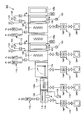
- the overall configuration of the film forming apparatus according to the embodiment of the present invention is shown. It is a figure which shows the structure of the film forming apparatus which concerns on one Embodiment of this invention, and shows the main component provided or connected to the pretreatment chamber, the transfer chamber, and the film forming chamber excluding the load / unload chamber.
- a schematic cross-sectional view of a film forming chamber of the film forming apparatus according to the embodiment of the present invention when viewed from above is shown.
- a detailed cross-sectional structure of an antenna for inductively coupled plasma generation used in the film forming apparatus according to the embodiment of the present invention is shown.
- a detailed cross-sectional structure of an antenna for inductively coupled plasma generation used in the film forming apparatus according to the embodiment of the present invention is shown.
- the schematic diagram when the plasma diffusion prevention plate provided in the film formation chamber of the film formation apparatus which concerns on one Embodiment of this invention is seen from the front is shown.
- the schematic diagram when the plasma diffusion prevention plate provided in the film formation chamber of the film formation apparatus which concerns on one Embodiment of this invention is seen from the front is shown. It is a figure explaining the influence which the antenna for inductively coupled plasma generation provided in a film forming chamber has on a substrate surface, and shows the case where there is no plasma diffusion prevention plate. It is a figure explaining the influence which the antenna for inductively coupled plasma generation provided in a film forming chamber has on a substrate surface, and shows the case where a plasma diffusion prevention plate is provided.
- a schematic cross-sectional view showing the configuration of the pretreatment chamber of the film forming apparatus according to the embodiment of the present invention is shown.
- the front view of the antenna for inductively coupled plasma generation provided in the film formation chamber of the film formation apparatus which concerns on one Embodiment of this invention is shown.
- a cross-sectional view of an antenna for inductively coupled plasma generation provided in a film forming chamber of a film forming apparatus according to an embodiment of the present invention is shown, and a cross-sectional structure corresponding to between A1 and A2 shown in FIG. 16A is shown.
- the front view of the antenna for inductively coupled plasma generation provided in the film formation chamber of the film formation apparatus which concerns on one Embodiment of this invention is shown.
- the cross-sectional view of the antenna for inductively coupled plasma generation provided in the film-forming chamber of the film-forming apparatus according to the embodiment of the present invention is shown, and the cross-sectional structure corresponding to between B1 and B2 shown in FIG. 17A is shown.
- An example of an element manufactured by using the film forming apparatus according to the embodiment of the present invention is shown.
- the detailed structure of the oxide semiconductor layer in the element manufactured by using the film forming apparatus which concerns on one Embodiment of this invention is shown.
- the detailed structure of the oxide semiconductor layer in the element manufactured by using the film forming apparatus which concerns on one Embodiment of this invention is shown.
- the overall configuration of the film forming apparatus according to the embodiment of the present invention is shown.
- FIG. 22A shows a front view of a ceramic member used in the film forming chamber shown in FIG. 22A.
- FIG. 23A shows a front view of a ceramic member used in the film forming chamber shown in FIG. 23A.
- a member or region is “above (or below)" another member or region, it is directly above (or directly below) the other member or region, unless otherwise specified. This includes not only certain cases but also cases above (or below) other members or areas. That is, it also includes the case where another component is included between the member or region above (or below) the other member or region.
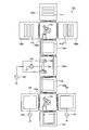
- FIG. 1 shows the overall configuration of a film forming apparatus 100 that performs sputtering film formation according to an embodiment of the present invention.
- the film forming apparatus 100 includes a load / unload chamber 102 in which a substrate before and after film formation is housed, a pretreatment chamber 104 for pretreating the substrate, and a first transfer chamber 106a provided with a transfer robot 116. It includes a second transfer chamber 106b provided with a platen mechanism 118, a first film forming chamber 108a for performing sputtering film formation, and a second film forming chamber 108b. These chambers are connected by a gate valve and are provided with vacuum exhaust means (not shown).
- the substrate on which the thin film is formed is stored in the load / unload chamber 102 while being held in the cassette.
- the substrate is, for example, a glass substrate.
- the substrate housed in the load / unload chamber 102 is transferred to the pretreatment chamber 104 by the transfer robot 116 provided in the first transfer chamber 106a.
- the pretreatment chamber 104 performs pretreatment on the substrate forming the thin film.
- the pretreatment chamber 104 includes a high frequency discharge electrode connected to the high frequency power supply 120. As the pretreatment, the substrate is degassed by the high frequency discharge plasma generated by the stage provided with the heating mechanism and the high frequency discharge electrode. FIG.
- FIG. 1 shows an embodiment in which two pretreatment chambers 104 are installed with the first transfer chamber 106a interposed therebetween, but the number of pretreatment chambers 104 is not limited.
- the film forming apparatus 100 is not limited to the form shown in FIG. 1, and the number of pretreatment chambers 104 may be one or three or more.
- the substrate pretreated in the pretreatment chamber 104 is conveyed to the second transfer chamber 106b by the transfer robot 116.
- the substrate is transported horizontally from the load / unload chamber 102 to the pretreatment chamber 104.
- the second transfer chamber 106b is provided with a platen mechanism 118, and the substrate carried in the horizontal state is tilted in a vertical state or a range of about 20 degrees from the vertical state so as to be held by a transfer carrier (not shown in FIG. 1). It can be set up in a vertical state.
- the first film forming chamber 108a and the second film forming chamber 108b are provided with an antenna 126 for inductively coupled plasma generation, and a sputtering target 124 is mounted on the first film forming chamber 108a and the second film forming chamber 108b.
- sputtering film formation is performed by inductively coupled plasma (ICP) generated by an antenna 126 for inductively coupled plasma generation.
- ICP inductively coupled plasma
- a pulse power supply 123 is connected to the sputtering target 124, and it is possible to control the acceleration energy of ions.
- the film forming apparatus 100 is capable of controlling the density of the thin film deposited on the substrate by such a mechanism.
- Sputtering targets 124 of different materials can be mounted on the first film forming chamber 108a and the second film forming chamber 108b, and thin films having different compositions can be continuously deposited in a vacuum. Can be done. Further, the first film forming chamber 108a and the second film forming chamber 108b may be equipped with sputtering targets 124 of the same type (component, composition, density), whereby different film qualitys may be applied by applying different film forming conditions. Thin film can be deposited.
- the film forming apparatus 100 is not limited to such a configuration, and the number of film forming chambers 108 is appropriately changed according to the structure and type of the thin film to be produced. be able to.
- the number of film forming chambers 108 may be one, and when forming a multilayer thin film, three or more film forming chambers 108 are connected. It may have been done.
- FIG. 2 is a diagram showing the configuration of the film forming apparatus 100, in which the pretreatment chamber 104 excluding the load / unload chamber, the first transfer chamber 106a, the second transfer chamber 106b, the first film forming chamber 108a, and the second formation chamber are shown.
- the main components provided or connected to the membrane chamber 108b are shown.
- a vacuum exhaust system 110 is connected to each chamber.
- the vacuum exhaust system 110 is composed of a vacuum pump such as a turbo molecular pump (TMP) and a dry pump (DRP).
- TMP turbo molecular pump
- DRP dry pump
- the configuration of the vacuum exhaust system 110 may be different or the same for the first transfer chamber 106a and the second transfer chamber 106b and the first film formation chamber 108a and the second film formation chamber 108b.
- the first film forming chamber 108a and the second film forming chamber 108b may be provided with a conductance valve for pressure control. Further, the gas supply system 112 is connected to the pretreatment chamber 104, the first film forming chamber 108a, and the second film forming chamber 108b.
- the gas supply system 112 includes a mass flow controller, a filter, and the like.
- the pretreatment chamber 104 is provided with a substrate stage 114 and a high frequency discharge electrode 115.
- the high frequency discharge electrode 115 is connected to the high frequency power supply 120.
- the substrate is pretreated by the high frequency discharge plasma generated by the substrate stage 114 and the high frequency discharge electrode 115.
- a first transfer chamber 106a provided with a transfer robot 116 and a second transfer chamber 106b provided with a platen mechanism 118 are provided between the pretreatment chamber 104 and the first film forming chamber 108a.
- the substrate on which the adsorbed molecules have been desorbed in the pretreatment chamber 104 is transferred to the first film forming chamber 108a via the first transfer chamber 106a and the second transfer chamber 106b without being exposed to the atmosphere.
- the substrate pretreated in the pretreatment chamber 104 is conveyed to the second transfer chamber 106b by the transfer robot 116 of the first transfer chamber 106a.
- the transfer robot 116 transfers the substrate while keeping it in a horizontal state.
- the substrate conveyed to the second transfer chamber 106b is erected vertically or tilted in a range of about 20 degrees from the vertical by the platen mechanism 118, and is carried into the first film forming chamber 108a.
- the film forming apparatus 100 provides a platen mechanism 118 in the middle of the transfer path of the substrate, handles the substrate horizontally until the stage before film formation, and handles the substrate vertically or vertically 20 in the film forming stage. Since the board is tilted within a range of degree, the substrate can be easily handled. Further, the film forming apparatus 100 has an advantage that the floor area required for installation can be reduced.
- the first film forming chamber 108a is provided with an antenna 126 for inductively coupled plasma generation, and a sputtering target 124 is attached to the first film forming chamber 108a.
- the antenna 126 for inductively coupled plasma generation is connected to a high frequency power supply 120 that outputs a high frequency in the megahertz band.
- the antenna 126 for inductively coupled plasma generation may be connected to an AC power supply 122 so that an AC voltage in the kilohertz band can be applied so as to be superimposed on high frequency power.
- the pulse power supply 123 is connected to the sputtering target 124 as described above.
- the first film forming chamber 108a may be provided with a heater 127 for heating the substrate.
- the second film forming chamber 108b also has the same configuration as the first film forming chamber 108a.
- the first film forming chamber 108a and the second film forming chamber 108b are provided with a transport mechanism for transporting the substrate in a vertical or tilted state within a range of about 20 degrees from the vertical.
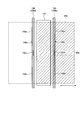
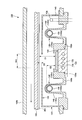
- FIG. 3 shows a partial cross-sectional schematic view of the film forming chamber 108 (first film forming chamber 108a, second film forming chamber 108b) when viewed from above.
- the film forming chamber 108 is configured to form a closed space in which the internal space is shielded from the atmosphere
- FIG. 3 shows a schematic diagram between two wall surfaces (first chamber wall 109a and second chamber wall 109b). Structure is shown.
- the film forming chamber 108 includes a plasma diffusion prevention plate 140 provided so as to cover the sputtering target 124, and an inductively coupled plasma generation antenna 126 (the first) provided so as to project into a region surrounded by the plasma diffusion prevention plate 140. 1 antenna 126a, 2nd antenna 126b) and a gas introduction tube 138 for introducing sputter gas.
- the film forming apparatus 100 is used in a state where the sputtering target 124 is attached to the film forming chamber 108, but the sputtering target 124 is a consumable item and is not a component fixed to the film forming apparatus 100, but is replaced as appropriate. It is an accessory member.
- Members such as a sputtering target 124 and an antenna 126 for inductively coupled plasma generation are attached to the film forming chamber 108, and a sealing member such as an O-ring and a gasket is provided at the attachment portion of each member.
- the sputtering target 124 includes a target material 132 and a backing plate 130.
- the target material 132 is bonded to a backing plate 130 made of a metal such as copper (Cu) or titanium (Ti) with a bonding material such as an indium alloy.
- the target material 132 is preferably an integrally molded product.
- the sputtering target 124 is attached to the first chamber wall 109a of the film forming chamber 108.
- the first chamber wall 109a is provided with a first through hole 128a, and the sputtering target 124 is attached so that the backing plate 130 is fitted into the first through hole 128a. Since a bias voltage is applied to the sputtering target 124, an insulating component 136 is provided between the backing plate 130 and the first chamber wall 109a.
- the sputtering target 124 has a rectangular shape when viewed from the front, and is provided in the longitudinal direction parallel to the vertical direction.
- Various sputterable materials can be attached to the target material 132.
- the target material 132 a transparent conductive film or a sintered body of a metal oxide for forming an oxide semiconductor film can be applied.
- the temperature of the target material 132 rises due to the collision of ions during the sputtering film formation. Therefore, the film forming apparatus 100 is provided with a mechanism for cooling the backing plate 130 in order to suppress the temperature rise of the target material 132.
- FIG. 3 shows, as an example, a structure in which the backing plate 130 is provided with a water flow hole for flowing cooling water.
- the target material 132 is exposed in the internal space of the film forming chamber 108.
- the film forming chamber 108 is provided with a shield plate 134 so as to cover the peripheral edge of the target material 132.
- the shield plate 134 is provided so as to cover the surface of the backing plate 130 exposed in the region between the target material 132 and the first chamber wall 109a.
- the film forming chamber 108 is provided with an antenna 126 (first antenna 126a, second antenna 126b) for inductively coupled plasma generation.
- the antenna 126 for inductively coupled plasma generation is arranged along the longitudinal direction of the sputtering target 124 and so as to sandwich the sputtering target 124. That is, the first antenna 126a and the second antenna 126b as the antenna 126 for inductively coupled plasma generation are arranged so as to sandwich the sputtering target 124.
- the first antenna 126a and the second antenna 126b as the antenna 126 for inductively coupled plasma generation have a U-shaped groove shape with the antenna main body 148 (first antenna main body 148a, second antenna main body 148b) for inductively coupled plasma generation.
- the antenna main body 148 first antenna main body 148a, second antenna main body 148b
- the first antenna main body 148a is provided in the first insulating member 146a
- the second antenna main body 148b is provided in the second insulating member 146b.
- the antenna 126 for inductively coupled plasma generation is provided so that the insulating member 146 is inserted into the second through hole 128b of the first chamber wall 109a and protrudes from both sides of the sputtering target 124.
- the antenna body 148 for inductively coupled plasma generation in the insulating member 146 in this way, the substance sputtered from the target material 132 does not adhere to the antenna body 148 for inductively coupled plasma generation. Can be done. Further, the antenna body 148 for inductively coupled plasma generation can be prevented from being exposed to inductively coupled plasma.
- the antenna body 148 for inductively coupled plasma generation protrudes at a position higher than the surface of the target material 132 (a position closer to the center in the film forming chamber 108 or a position on the substrate 200 side). It is provided to do so.
- the antenna body 148 for inductively coupled plasma generation is provided so as to project from the surface of the target material 132 by the length D2. In this way, by providing the antenna body 148 for inductively coupled plasma generation so as to project from the surface of the target material 132, the plasma density can be increased on the surface of the target material 132.
- FIG. 22A shows another configuration of the film forming chamber 108 (first film forming chamber 108a, second film forming chamber 108b).
- FIG. 22A shows a partial cross-sectional schematic view of the film forming chamber 108 when viewed from above, as in FIG.
- a part of the first chamber wall 109a to which the antenna 126 (first antenna 126a, second antenna 126b) for inductively coupled plasma generation and the sputtering target 124 are attached is formed of a ceramic member 180a.
- the structure is shown.
- FIG. 22B shows a front view of the ceramic member 180a.
- the ceramic member 180a is provided with a first through hole 128a to which the sputtering target 124 is attached. Since the ceramic member 180a has an insulating property, the sputtering target 124 can be directly attached. That is, when the sputtering target 124 is attached to the film forming chamber 108, the insulating component 136 as shown in FIG. 3 can be omitted. Further, the ceramic member 180a is provided with a second through hole 128b for attaching an antenna 126 (first antenna 126a, second antenna 126b) for inductively coupled plasma generation.
- the U-shaped groove-shaped insulating member 146 (first insulating member 146a, second insulating member 146b) is inserted through the second through hole 128b and vacuum-sealed by an O-ring on the back surface side of the ceramic member 180a. Further, since the ceramic member 180a is insulating, the shield plate 134 that covers the peripheral edge of the target material 132 can be integrated.
- FIG. 23A shows an antenna body 148 (first) in which a part of the first chamber wall 109a is inductively coupled to the ceramic member 180b in the film forming chamber 108 (first film forming chamber 108a, second film forming chamber 108b). It shows a structure in which a U-shaped groove-shaped insulating member 146 (first insulating member 146a, second insulating member 146b) covering the antenna main body 148a and the second antenna main body 148b) is integrated. Further, FIG. 23B shows a front view of the ceramic member 180b. As shown in FIGS.
- the number of parts is increased by integrally molding the U-shaped groove-shaped insulating member 146 (first insulating member 146a, second insulating member 146b) with a part of the first chamber wall 109a. It can be reduced and leaks (vacuum airtight leaks) can be prevented. Further, on the atmospheric side (the side where the antenna body 148 for inductively coupled plasma generation is provided) of the portion corresponding to the insulating member (first insulating member 146a, second insulating member 146b) having a U-shaped groove shape of the ceramic member 180b. A glass layer may be formed. By providing the glass layer, the leakage from the atmosphere side can be further reduced.
- the ceramic members 180a and 180b are suitably used as wall materials for the film forming chamber 108 because they not only have excellent insulating properties, but also have a high heat resistant temperature, a small coefficient of thermal expansion, can be precision machined, and have a small amount of outgassing. be able to.
- the ceramic members 180a and 180b for the wall material near the antenna 126 for inductively coupled plasma generation the power loss of the antenna 126 for inductively coupled plasma generation can be reduced. Thereby, the plasma density near the surface of the target material 132 can be increased.
- the amount of degassing from the inner wall of the chamber can be reduced and the plasma density can be increased. Can be done. Further, since the peripheral portion of the target material 132 is composed of ceramic members 180a and 180b which are insulating members, the region where a vertical electric field is generated with respect to the surface of the target material 132 can be expanded, and a film having a higher density can be formed. Can be made.
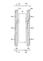
- FIG. 4 shows a detailed cross-sectional structure of the antenna 126 for inductively coupled plasma generation.
- the antenna body 148 for inductively coupled plasma generation is formed of a hollow metal tube 150.
- the antenna body 148 for inductively coupled plasma generation is formed of a hollow metal tube 150 made of copper (Cu), brass, aluminum (Al), or the like.
- the antenna body 148 for inductively coupled plasma generation forms a rod-shaped antenna by such a metal tube, and cooling water is flowed through the hollow portion.
- a conductive layer 151 formed of a nickel (Ni) or tin (Sn) plating film is formed on the inner surface of the metal tube 150 in order to prevent corrosion.
- the insulating member 146 is made of quartz or ceramics such as alumina, ytria (Y 2 O 3 ), forsterite (Mg 2 SiO 4 ), and steatite (Mg O ⁇ SiO 2).
- the insulating member 146 is a U-shaped groove-shaped member in which the antenna body 148 for inductively coupled plasma generation is arranged, and is arranged so as to separate the vacuum from the atmosphere. It is preferable that the surface of the insulating member 146 (particularly the surface on the atmospheric side) is provided with a glass layer 147 in order to improve airtightness (to prevent leakage).
- the antenna body 148 for inductively coupled plasma generation is arranged on the atmosphere side by being passed through the insulating member 146.
- the antenna body 148 for inductively coupled plasma generation By arranging the antenna body 148 for inductively coupled plasma generation on the atmosphere side in this way, the accuracy of the installation position can be improved, and the uniformity of the plasma density in the vicinity of the target material 132 can be improved. Further, the holding mechanism of the antenna body 148 for inductively coupled plasma generation can be freely designed.
- the antenna 126 for inductively coupled plasma generation may be configured to include a plurality of antenna bodies 148 for inductively coupled plasma generation. That is, the antenna main body 148 for inductively coupled plasma generation may be composed of a plurality of antenna main bodies 148 for inductively coupled plasma generation, and may be arranged on the atmospheric side of the insulating member 146.
- the metal tube 150 constituting the antenna body 148 for inductively coupled plasma generation has an AC resistance that increases as the frequency increases due to the skin effect. For example, when a high frequency power of 13.56 MHz is applied to the antenna body 148 for inductively coupled plasma generation, the current is about 17.7 ⁇ m from the surface of the metal tube 150 even if the wall thickness of the metal tube 150 is 5 mm. Only the depth area will flow.
- the antenna 126 for inductively coupled plasma generation may have a plurality of antenna bodies 148 for inductively coupled plasma generation arranged in parallel as shown in FIG.
- the gas introduction pipe 138 is a region inside the plasma diffusion prevention plate 140 and is provided adjacent to the first antenna 126a.
- the gas introduction pipe 138 is provided for introducing the sputter gas into the film forming chamber 108.
- the gas introduction tube 138 is provided along the longitudinal direction of the sputtering target 124 like the antenna 126 for inductively coupled plasma generation.
- the gas introduction pipe 138 may have a structure in which a shower nozzle is provided in a metal pipe, but it is preferably formed of an insulating porous body, for example, a ceramic porous body tube. .. By using a porous body for the gas introduction pipe 138, the sputtering gas can be uniformly introduced along the longitudinal direction of the sputtering target 124.
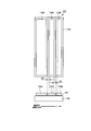
- the plasma diffusion prevention plate 140 is provided so as to surround the region where the sputtering target 124 is arranged.
- the plasma diffusion prevention plate 140 is a box-shaped member, and is provided inside the film forming chamber 108 so as to form a space surrounded by the first chamber wall 109a and the plasma diffusion prevention plate 140.
- the plasma diffusion prevention plate 140 has a first surface 142 substantially parallel to the surface of the first chamber wall 109a, and a second surface 143 from the first surface 142 toward the first chamber wall 109a.
- the adhesion plate 141 is provided so as to cover the surface of the first chamber wall 109a.
- a first opening 144 is provided on the first surface 142 of the plasma diffusion prevention plate 140. The first opening 144 is provided at a position overlapping with the target material 132.
- FIG. 6 shows a schematic view of the structure of the plasma diffusion prevention plate 140 when viewed from the front.
- the sputtering target 124 is provided in a region surrounded by the plasma diffusion prevention plate 140.
- the target material 132 is exposed from the first opening 144 of the plasma diffusion prevention plate 140.
- the antenna 126 for inductively coupled plasma generation (first antenna 126a, second antenna 126b) is arranged at a position covered by the plasma diffusion prevention plate 140.
- the first antenna body 148a has a structure in which the first metal tube 150a and the second metal tube 150b are connected via the first capacitor 152a, and the second antenna body 148b has the third metal tube 150c and the fourth metal.
- the tube 150d has a structure connected via a second capacitor 152b.
- the plasma diffusion prevention plate 140 is provided with a slit-shaped second opening 154 from the second surface 143 to the first surface 142.
- a plurality of second openings 154 are provided so as to extend in a direction intersecting the longitudinal direction of the antenna 126 for inductively coupled plasma generation.
- the second opening 154 is an orifice for sputter gas, and has a function of controlling the flow of sputter gas supplied to the space surrounded by the plasma diffusion prevention plate 140. That is, the second opening 154 controls the conductance of the gas flow so that the sputter gas stays in the space surrounded by the plasma diffusion prevention plate 140 for a predetermined time and forms a uniform gas pressure in the film forming area.
- the slit-shaped second opening 154 has a function of preventing an inductive current generated in the plasma diffusion prevention plate 140 by the inductively coupled plasma generation antenna 126, and is inductively coupled from the inductively coupled plasma generation antenna 126.
- the efficiency of energy transfer to plasma can be increased.
- the plasma diffusion prevention plate 140 is preferably made of a material having a secondary electron emission rate of more than 1.
- the plasma diffusion prevention plate 140 is preferably formed of an aluminum-based magnesium alloy, barium alloy, or calcium alloy. Further, it is preferable that the inner surface of the plasma diffusion prevention plate 140 made of these metal materials facing the sputtering target 124 is anodized.
- the secondary electron emission ratio can be made larger than 1 by forming an anodized film of a magnesium alloy, a barium alloy, or a calcium alloy on the inner surface of the plasma diffusion prevention plate 140.
- the surface of the anodic oxide film is positively resistant to electricity, and argon ions (plus ions) can be prevented from entering or colliding with the plasma diffusion prevention plate 140. That is, sputtering of the plasma diffusion prevention plate 140 by argon ions (plus ions) is prevented, and impurities incorporated into the thin film formed in the film forming chamber 108 can be reduced.
- the carrier concentration of the n-type oxide semiconductor film is precisely controlled by sputtering, it is necessary to prevent the inclusion of impurities that cause an electron killer effect.
- the insulating film from which the electron killer effect does not occur include silicon oxide (SiO 2 ), magnesium oxide (MgO), and alumina (Al 2 O 3 ).
- magnesium oxide (MgO) having a high secondary electron emission rate is preferable, and it is preferable to cover the surface of the plasma diffusion prevention plate 140 with magnesium oxide (MgO) -containing silicon oxide, aluminum oxide or the like.
- the plasma diffusion prevention plate 140 is provided so that the inductively coupled plasma formed by the antenna 126 for generating the inductively coupled plasma does not spread to the entire film forming chamber 108.
- the plasma diffusion prevention plate 140 By forming a physical wall called the plasma diffusion prevention plate 140, it is possible to prevent the inductively coupled plasma from spreading unnecessarily in the film forming chamber 108. That is, the film forming chamber 108 has a structure in which inductively coupled plasma is generated in a region surrounded by the plasma diffusion prevention plate 140 and the adhesion plate 141, and inductively coupled plasma does not spread to other regions. Since the anodic oxide film is formed on the surface of the plasma diffusion prevention plate 140 and the adhesion plate 141, the plasma confinement action can be enhanced and the plasma density can be increased.
- the conventional magnetron sputtering apparatus in order to improve the film density of the oxide semiconductor film formation, it is required to keep the gas pressure at the time of film formation at 0.5 Pa or less. Furthermore, it is necessary to pay attention not only to the impurity gas separated from the inner wall of the film forming chamber, but also to the fact that the braiding material inside the film forming chamber is sputtered and taken into the film as impurities.
- Oxide semiconductors typified by InGaSnO x have an n-type conductive type, so the film formation chamber is made of stainless steel containing iron (Fe), chromium (Cr), manganese (Mn), etc., which has a large electron killer effect. When made, it is necessary to completely prevent the chamber wall from coming into contact with the plasma. When forming the oxide semiconductor film, the water adsorbed on the substrate surface (H 2 O), if not perform processing of separating the hydrocarbon and the like, a highly reliable thin film transistor not film density is high Cannot be made.
- the film forming chamber 108 has a structure in which the inductively coupled plasma is confined by the plasma diffusion prevention plate 140 and the adhesion plate 141, the film forming chamber 108 is formed on the chamber wall 109 (first chamber wall 109a, second chamber wall 109b, etc.). It is possible to prevent the adsorbed impurities (moisture (H 2 O), hydrogen (H 2 ), hydrocarbon, etc.) from being incorporated into the thin film deposited on the substrate. Even when the film forming chamber 108 is made of stainless steel (SUS304), the problem of contamination by iron (Fe), chromium (Cr) and the like can be prevented.
- a mesh 170 may be provided in the first opening 144.
- the mesh 170 is preferably made of a metal material that does not have an electron killer effect.
- the mesh 170 is preferably made of a metal material selected from titanium (Ti), tungsten (W), nickel (Ni), and tantalum (Ta). This reliably prevents the spread of plasma into the film forming chamber 108, and also prevents impurities that become electron killer from being incorporated into the film when the oxide semiconductor film is deposited. can.
- the aperture ratio of the mesh 170 is preferably 70% or more.
- the wires (or mesh patterns) forming the mesh 170 are arranged so as to tilt and intersect in a range of 30 to 60 degrees with respect to the moving direction (horizontal direction) of the substrate. , It is possible to prevent the pattern of the mesh 170 from being transferred to the film on which the film is formed.
- the plasma diffusion prevention plate 140 is provided so as to be interposed between the antenna 126 (first antenna 126a, second antenna 126b) for inductively coupled plasma generation and the substrate 200. If the plasma diffusion prevention plate 140 is not provided, as shown in FIG. 8A, the antenna 126 for inductively coupled plasma generation (first antenna 126a, second antenna 126b) affects the film quality of the thin film deposited on the substrate 200. Giving is a problem. That is, the surface 202 of the substrate 200 adjacent to the antenna 126 for inductively coupled plasma generation (first antenna 126a, second antenna 126b) is the antenna 126 for inductively coupled plasma generation (first antenna 126a, second antenna 126b).
- the film quality of the deposited thin film is significantly different.
- the plasma diffusion prevention plate 140 when the plasma diffusion prevention plate 140 is interposed between the antenna 126 for inductively coupled plasma generation (first antenna 126a, second antenna 126b) and the substrate 200, the effect of self-bias is obtained. Is shielded, so that the film quality of the thin film deposited on the substrate 200 can be kept constant.
- the antenna 126 for inductively coupled plasma generation has a connecting region (a region in which two conductors are capacitively coupled, the details of which will be described later), the plasma diffusion prevention plate 140 prevents plasma. The problem of uniformity can be solved.
- inductively coupled plasma is also shown in FIG.
- a capacitor 152 (first capacitor 152a, second capacitor) connecting the metal tubes 150 (first metal tube 150a and second metal tube 150b, third metal tube 150c and fourth metal tube 150d) constituting the antenna main body 148 for generation.
- the problem is that the film quality of the region overlapping with 152b) is different.
- the plasma diffusion prevention plate 140 when the plasma diffusion prevention plate 140 is not provided, the plasma densities of the portions of the first capacitor 152a and the second capacitor 152b provided in the first antenna 126a and the second antenna 126b are different and overlap with the portions. Since it affects the film quality of the thin film deposited on the antenna connecting region 204, it becomes impossible to form a uniform thin film on the entire surface of the substrate 200. On the other hand, when the plasma diffusion prevention plate 140 is provided, the region corresponding to the antenna connecting region 204 does not exist, and the influence of the plasma non-uniformity disappears, so that the entire surface of the substrate 200 is uniform. It is possible to form a flexible film.
- the film forming apparatus 100 is a mobile film forming method, and as shown in FIG. 3, the substrate 200 is mounted on the conveying tray 160 and conveyed in front of the sputtering target 124. The substrate 200 is conveyed at a position close to the plasma diffusion prevention plate 140. As shown in FIG. 3, the distance from the surface of the target material 132 to the surface of the substrate 200 is D1, and the distance between the surface of the substrate 200 and the surface of the plasma diffusion prevention plate 140 is D3. In this case, the plasma diffusion prevention plate 140 and the transport tray 160 are arranged so that the interval D3 is 1/5 or less of the distance D1. For example, if the distance D1 is 55 mm, the spacing D3 has a length of 5 mm.
- the sputter gas supplied to the region surrounded by the plasma diffusion prevention plate 140 is passed through the first opening 144 into the film forming chamber 108. It is possible to reduce the conductance when flowing out to the plasma. Further, this configuration has an effect of preventing impurities (moisture (H 2 O), hydrogen (H 2 ), hydrocarbon, etc.) adsorbed on the chamber wall 109 from diffusing and flowing into the film formation region. The effect of improving the reproducibility of the physical properties of the thin film to be filmed can be exhibited.
- FIG. 10A and 10B show an example of the sputtering target 124 applicable to the mobile film forming method.
- FIG. 10A shows a structure in which two types of target materials 132 (first target material 132a and second target material 132b) are fixed to the backing plate 130 by the bonding material 131. Indium or an indium alloy is used as the bonding material 131.
- the first target material 132a and the second target material 132b are combined with different compositions or materials.
- the target material is an oxide semiconductor
- a ternary oxide semiconductor target containing indium (In), gallium (Ga), and tin (Sn) is used as the first target material 132a
- the second target is used.
- an oxide semiconductor target having a higher concentration of gallium (Ga) than that of the first target material 132a is used.
- the first target material 132a and the second target material 132b are arranged at predetermined intervals on the backing plate 130 in order to prevent damage due to thermal expansion.
- the interval G1 is about 0.5 mm.
- the ends of the first target material 132a and the second target material 132b are formed in a tapered shape in a cross-sectional view so that the backing plate 130 or the bonding material 131 is not exposed at the separated portion.
- the first target material 132a has a tapered surface formed so that the end portion on the upper surface side protrudes from the bottom surface in contact with the bonding material 131, and the second target material 132b has an upper surface surface.
- a tapered surface is formed in which the bottom surface projects with respect to the side.
- the backing plate 130 and the bonding material 131 are not exposed when the sputtering target 124 is viewed in a plan view. can do. That is, even when two types of target materials are arranged on one backing plate 130, the backing plate 130 and the bonding material 131 can be prevented from being sputtered at the boundary region, and impurities are incorporated into the film on which impurities are deposited. Can be avoided.
- the thin film deposited by narrowing the width of the second target material 132b with respect to the first target material 132a.
- the film thickness can be different. For example, by narrowing the width of the second target material 132b with respect to the width of the first target material 132a, the film thickness of the thin film deposited on the first target material 132a is increased, and the film is deposited on the second target material 132b. The film thickness of the thin film can be reduced.
- FIG. 10B shows an example in which three types of target materials 132 (first target material 132a, third target material 132c, second target material 132b) are arranged. Also in this case, similarly to the example shown in FIG. 10A, the side end portions where the target materials are adjacent to each other are formed in a tapered shape. Specifically, the third target material 132c sandwiched between the first target material 132a and the second target material 132b has a trapezoidal cross-sectional shape. By arranging the first target material 132a and the second target material 132b having opposite tapered surfaces from both sides of the third target material 132c having such a cross-sectional shape, the sputtering target 124 can be bonded to the backing plate 130 or the bonding.
- the material 131 has a structure that is not exposed in a plan view.
- FIG. 11 shows the details of the antenna 126 (first antenna 126a, second antenna 126b) for inductively coupled plasma generation.
- the first antenna 126a includes a first insulating member 146a and a first antenna body 148a
- the second antenna 126b includes a second insulating member 146b and a second antenna body 148b.
- the first antenna main body 148a is a rod-shaped antenna in which the first metal tube 150a and the second metal tube 150b are connected via the first antenna 152a formed in the antenna connecting region 204
- the second antenna main body 148b is a rod-shaped antenna.
- the impedance of the first antenna main body 148a and the second antenna main body 148b can be reduced by having such a structure. As a result, even when the antenna body 148 for inductively coupled plasma generation is lengthened, it is possible to prevent an increase in impedance and prevent a large potential difference from occurring at both ends of the antenna body 148 for inductively coupled plasma generation. As a result, it is possible to cope with an increase in the size of the sputtering target 124.
- FIG. 12 shows the cross-sectional structure of the antenna connecting region 204 of the antenna body 148 for inductively coupled plasma generation.
- the antenna connecting region 204 has a structure in which the first metal tube 150a and the second metal tube 150b (or the third metal tube 150c and the fourth metal tube 150d) are fitted in a hollow tube 172 formed of an insulating material. ..
- An O-ring 153 is provided at a portion where the hollow pipe 172 fits with the first metal pipe 150a and the second metal pipe 150b to maintain airtightness, and has a structure that does not leak even if cooling water flows. There is.
- the O-ring 153 preferably has heat resistance, and for example, a fluororubber-based O-ring is used.
- a conductive layer 174 used as an electrode of the capacitor 152 is formed on the inner surface of the hollow tube 172.
- the first conductive layer 174a is formed by copper plating in order to reduce the resistance
- the second conductive layer 174b is nickel (Ni) plated or tin (Sn) plated in order to prevent corrosion of the copper plating film. Is formed by.
- the conductive layer 151 is also formed on the inner surfaces of the first metal tube 150a and the second metal tube 150b.
- the conductive layer 174 is arranged so as to face the first metal tube 150a and the second metal tube 150b via the hollow tube 172 formed of the insulating material, whereby the capacitor 152 is formed. That is, the first metal tube 150a and the second metal tube 150b are capacitively coupled by being fitted into a hollow tube 172 having a conductive layer 174 formed on the inner surface to form an antenna body 148 for inductively coupled plasma generation. is doing.
- the hollow tube 172 formed of the insulating material By arranging the hollow tube 172 formed of the insulating material in the inner peripheral portions of the first metal tube 150a and the second metal tube 150b, the unevenness of the antenna body 148 for inductively coupled plasma generation is reduced and the inductively coupled. It is possible to make the plasma uniform.
- the antenna body 148 for inductively coupled plasma generation is provided on the atmosphere side, a variable capacitor 176 can be provided in parallel with the capacitor 152. As a result, the impedance of the antenna body 148 for inductively coupled plasma generation can be adjusted precisely and in a wide range. As a result, the antenna 126 for inductively coupled plasma generation can be easily matched with the high frequency power supply 120.
- the condenser 152 is provided in the flow path of the cooling water (because the condenser 152 is in contact with the cooling water), the heat generation of the condenser 152 can be effectively suppressed. can. With such a configuration, it is possible to prevent failure and destruction due to heat generation of the capacitor 152, and it is also possible to increase the high frequency power applied to the antenna 126 for inductively coupled plasma generation.
- the antenna body 148 for inductively coupled plasma generation is divided into two or more as shown in FIGS. 16 and 17, and connected in series via a variable capacitor 176 for resonance. It can be resolved.
- the antenna body 148 for inductively coupled plasma generation is connected to a high frequency power supply 120 having an oscillation frequency of 13.56 MHz or 27 MHz.
- the first antenna main body 148a is connected to the first high frequency power supply 120a
- the second antenna main body 148b is connected to the second high frequency power supply 120b.
- the first high-frequency power supply 120a and the second high-frequency power supply 120b may have the same phase of output high-frequency power, but rather preferably deviated by half a wavelength (180 degrees). Thereby, the plasma density on the surface of the target material 132 can be increased.
- first antenna main body 148a is also connected to the first variable capacitance capacitor 158a
- second antenna main body 148b is connected to the second variable capacitance capacitor 158b.
- the variable capacitance capacitor 158 adjusts the impedance of the antenna main body 148 (first antenna main body 148a and second antenna main body 148b) for inductively coupled plasma generation, and has a high frequency. It is provided to facilitate impedance matching with the power supply 120 (first high frequency power supply 120a, second high frequency power supply 120b).
- the antenna body 148 for inductively coupled plasma generation (first antenna body 148a, second antenna body 148b) is also connected to an AC power supply 122 having a frequency of 10 kHz to 1000 kHz.
- a coil 156 for blocking high frequencies is inserted between the antenna main body 148 (first antenna main body 148a, second antenna main body 148b) for inductively coupled plasma generation and the AC power supply 122.
- the deposit (the product sputtered from the target material 132) adhering to the insulating member 146 can be removed by the sputtering phenomenon.
- the circuit configuration of the antenna 126 for inductively coupled plasma generation shown in FIG. 11 exerts an advantageous effect in obtaining a stable discharge.
- the AC power supply 122 is not indispensable because even if deposits adhere to the insulating member 146, they are not significantly affected.
- the plasma density in the central region of the sputtering target 124 decreases, so the first antenna main body 148a and the second antenna are used by using the AC power supply 122.
- the plasma density can be made uniform.
- a pulse power supply 123 is connected to the sputtering target 124.
- the pulse power supply 123 applies a negative pulse voltage of about ⁇ 100 V to ⁇ 600 V to the sputtering target 124.
- the negative pulse voltage is applied at the timing when the AC voltage applied to the antenna main body 148 for inductively coupled plasma generation becomes 0 V, so that the sputtering particles are emitted in the direction perpendicular to the substrate. Is possible. Thereby, a dense film can be deposited.
- FIG. 14 schematically shows the relationship between the target voltage and the film density when an InGaZnO film is sputtered and formed as an oxide semiconductor film.
- the advantage of the sputtering method using inductively coupled plasma is that it is possible to separate and control two power sources, a power source that generates and maintains plasma and a power source that controls sputtering film formation. be.
- the voltage applied to the sputtering target is ⁇ 300 V or less, plasma generation becomes non-uniform and stable discharge cannot be maintained.
- inductively coupled plasma when using inductively coupled plasma, it is possible to generate a large amount of negative oxygen ions and oxygen radicals by increasing the high frequency power applied to the antenna for inductively coupled plasma generation to increase the plasma density.
- the plasma is not confined in the vicinity of the sputtering target by the magnetic field of the magnet, so that the plasma can be uniformly contacted with the surface of the substrate. This makes it possible to promote the oxidation reaction between the metal and the oxygen atom.
- the voltage applied to the sputtering target is set to about -200V, so that the crystal can be crystallized while minimizing the damage to the film deposited on the substrate surface.
- the conversion rate can be increased.
- the film density of the InGaZnO film can be 6.30 g / cm 3. This film density is close to the theoretical value of 6.378 g / cm 3.
- the film forming apparatus 100 using the inductively coupled plasma of the present embodiment can increase the film density of oxide semiconductor films having various compositions including the InGaZnO film, and has a threshold voltage Vth of the thin film transistor. The shift amount can be reduced. In other words, the film forming apparatus 100 using the inductively coupled plasma of the present embodiment can enhance the long-term reliability of the thin film transistor.
- FIG. 15 shows the configuration of the pretreatment chamber 104.
- the pretreatment chamber 104 is provided with a substrate stage 114 and a high frequency discharge electrode 115.
- the substrate stage 114 is provided with an elevating mechanism 164 that floats the mounted substrate 200 upward.
- the substrate stage 114 is provided with pins 162 in contact with the substrate 200 at a plurality of locations, and has a function of lifting the substrate 200 in a floating state by projecting the pins 162 upward by the elevating mechanism 164.
- the substrate stage 114 is formed of a conductor to function as a ground electrode and has the same potential as the chamber wall of the pretreatment chamber 104.
- the substrate stage 114 may include a heater for heating a substrate (not shown).
- the high frequency discharge electrode 115 is arranged so as to face the substrate stage 114.
- the high frequency discharge electrode 115 and the substrate stage 114 are connected to a high frequency power supply 120 having an oscillation frequency of 13.56 MHz or 27 MHz.
- the pretreatment chamber 104 is also provided with a gas introduction pipe 166.
- nitrogen (N 2 ) gas, oxygen (O 2 ) gas, or nitrous oxide (N 2 O) gas is introduced from the gas introduction pipe 166 as the pretreatment gas.
- a high frequency discharge electrode 115 formed of a shower plate may be used so that gas can be introduced from the high frequency discharge electrode 115.
- the pressure at the time of generating plasma in the pretreatment time is preferably in the range of 10 3 Pa from 10 Pa.
- high frequency discharge plasma 168 is generated.
- the substrate 200 is lifted by the pin 162 and installed in a floating state on the substrate stage 114.
- the high-frequency discharge plasma 168 is generated so as to wrap around not only the front surface side of the substrate 200 but also the back surface side. This makes it possible to remove molecules of impurities and contaminants such as water adsorbed on the back surface and the side surface as well as the front surface (the surface on which the thin film is deposited) of the substrate 200.
- the pin 162 is exposed to plasma, it is preferably formed of insulating ceramics so as not to emit impurities.
- plasma treatment in vacuum has been performed as a pretreatment for the substrate 200.
- the plasma treatment is performed only on the front surface side of the substrate 200, and the back surface side is not exposed to plasma.
- the moisture adsorbed on the back surface side remains, so that degassing from the back surface continues even after the substrate 200 is transported to the film forming chamber. ..
- the gas pressure at the time of sputter film formation is low as in the film formation of an oxide semiconductor film, the degassing treatment of only one side of the surface of the substrate 200 is insufficient.
- the film quality differs greatly between the vicinity of the center and the vicinity of the periphery.
- the carrier concentration differs greatly between the vicinity of the center and the vicinity of the periphery of the substrate 200 because the degassing component emitted from the back surface of the substrate 200 cannot be controlled. Will end up. The larger the size of the substrate 200, the greater this problem.
- the pretreatment chamber 104 by floating the substrate 200 and performing plasma treatment, not only the front surface but also the back surface is exposed to plasma, so that the entire surface can be degassed for a short time.
- the entire surface of the substrate can be cleaned, and the carrier concentration can be precisely controlled.
- the important points in the film forming apparatus 100 for forming the oxide semiconductor film are the adsorption components (moisture (H 2 O) and hydrogen (H 2) adsorbed on the entire surface of the substrate 200 before the sputtering film formation. ), Hydrocarbon) is forcibly degassed with nitrogen plasma or oxygen plasma. This makes it possible to produce a homogeneous oxide semiconductor film having a constant carrier concentration over the entire surface of the substrate 200.
- the film forming chamber 108 of the film forming apparatus 100 described above is preferably made of a metal material with less degassing.
- a metal material with less degassing For example, when forming an oxide semiconductor film for forming a thin film transistor, it is necessary to increase the film density in order to improve reliability. In order to increase the film density, it is necessary to carry out the sputtering pressure at the time of sputtering film formation at about 0.1 Pa to 1.5 Pa. In such a pressure range, the inductively coupled plasma spreads over the entire film formation chamber 108, exposing the inner wall to the plasma. When the positive ions in the plasma collide with the inner wall of the film forming chamber, a large amount of adsorbed molecules such as water (H 2 O), hydrogen (H 2 ), and hydrocarbon are detached. These impurities cause the characteristics of the transistor formed of the oxide semiconductor film to be affected.
- Stainless steel is used for the film forming chamber 108 of the film forming apparatus 100 shown in the present embodiment in consideration of strength.
- elements such as iron (Fe), molybdenum (Mo), and manganese (Mn), which are components of stainless steel, are not preferable because they become electron killer impurities with respect to n-type oxide semiconductors. That is, if the stainless steel is exposed in the film forming chamber 108, the characteristics of the transistor using the oxide semiconductor film are adversely affected.
- stainless steel is used as it is exposed in the film forming chamber, which is a factor of lowering the manufacturing yield of the transistor using the oxide semiconductor film and lowering the reproducibility of the process.
- the film forming apparatus 100 has magnesium (Mg), aluminum (Al), titanium (Ti), tungsten (W), and nickel in the film forming chamber 108.
- a plasma diffusion prevention plate 140 made of a metal such as (Ni) is provided to confine the plasma.
- magnesium oxide (MgO), barium oxide (BaO), and strontium oxide (SrO) having a high secondary electron emission rate are placed on the surface of the plasma diffusion prevention plate 140.
- a film of an oxide of an alkaline earth metal such as calcium oxide (CaO)
- a structure in which an insulating film containing silicon oxide, aluminum oxide, yttrium oxide or the like containing these is provided is adopted.
- the film forming apparatus 100 is provided with a first film forming chamber 108a and a second film forming chamber 108b.
- the configuration of the first film forming chamber 108a and the second film forming chamber 108b makes it possible to laminate two types of oxide semiconductor films having different film qualities.
- the first oxide semiconductor film can be deposited in the first film forming chamber 108a
- the second oxide semiconductor film can be deposited in the second film forming chamber 108b.
- a film is formed using only argon (Ar) or argon (Ar) and oxygen (O 2 ) as a sputter gas using a target of an oxide semiconductor, and a second film forming chamber is formed.
- argon (Ar) and oxygen (O 2 ) can be used (at this time, the oxygen partial pressure is made higher than the condition in the first film forming chamber 108a), and film formation can be performed.
- the density of negative oxygen ions can be increased by increasing the oxygen partial pressure, and the irradiation density of negative oxygen ions on the deposited surface of the thin film can be increased.
- the oxide semiconductor film deposited in the second film forming chamber 108b can reduce the carrier density and enhance the crystallinity with respect to the oxide semiconductor film deposited in the first film forming chamber 108a. Is possible.
- the negative ions of oxygen generated during the discharge reach the deposited surface of the oxide semiconductor film during the application of the pulse voltage, and promote the densification of the film. It can be easily crystallized.
- the antenna 126 for inductively coupled plasma generation can generate a large amount of oxygen radicals, and the inductively coupled plasma comes into contact with or close to the surface of the substrate 200, so that the metal element easily reacts with oxygen. Therefore, the probability that unreacted oxygen (O 2 ) molecules are incorporated into the membrane can be reduced.
- the film forming apparatus 100 adopts a mobile film forming method and has a configuration in which a plurality of first film forming chambers 108a and a plurality of second film forming chambers 108b are connected in series.
- the carrier concentration can be precisely controlled.
- an example of producing an oxide semiconductor film with the film forming apparatus 100 is mainly described, but the film forming apparatus 100 is not limited to this, and the film forming apparatus 100 includes a transparent conductive film, another semiconductor film, and a metal film. It can also be applied to the production of.
- the first antenna 126a and the second antenna 126b are sputtered.
- An example of a rod-shaped antenna extending in the same direction as the longitudinal direction of the target 124 and having substantially the same length is shown.
- the first insulating member 146a and the second insulating member 146b having a U-shaped groove shape are provided so as to project inside the region surrounded by the first chamber wall 109a and the plasma diffusion prevention plate 140.
- the 1 antenna main body 148a and the 2nd antenna main body 148b are provided so as to be surrounded by the first insulating member 146a and the second insulating member 146b having a U-shaped groove shape.
- first antenna 126a and the second antenna 126b are not limited to the forms shown in FIGS. 16A and 16B, and the U-shaped first antenna 126a and the second antenna 126b are each divided into a plurality of arrangements. May be good.
- a plurality of first antenna main bodies 148a_1 to 148a_3 and a plurality of second antenna main bodies 148b_1 ⁇ 148b_3 may be divided along the longitudinal direction of the sputtering target 124.
- 17A and 17B show an embodiment in which the antenna body 148 for inductively coupled plasma generation is divided into three and arranged in the longitudinal direction of the sputtering target 124, but the first antenna 126a for inductively coupled plasma generation is arranged.
- the number of the antenna main body 148 for inductively coupled plasma generation is not limited in the second antenna 126b, and the antenna for inductively coupled plasma generation in which the antenna main body 148 for inductively coupled plasma generation is divided into three or more is arranged. It may have been.
- FIG. 18A shows an example of an element manufactured by using the film forming apparatus 100.
- An example of the element is a transistor
- FIG. 18A shows the cross-sectional structure of the transistor 230.
- the transistor 230 includes an oxide semiconductor layer 216 formed on the substrate 200 by the film forming apparatus 100.
- the transistor 230 is formed on the first insulating layer 210 formed on the surface of the substrate 200.
- a first conductive layer 212a forming a source electrode and a first conductive layer 212b forming a drain electrode are provided in pairs.
- the first conductive layers 212a and 212b are formed of, for example, a transparent conductive film such as indium tin oxide (ITO) and indium zinc oxide (IZO).
- Second conductive layers 214a and 214b made of a metal material such as aluminum (Al) may be provided on the first conductive layers 212a and 212b in order to reduce the resistance.
- the oxide semiconductor layer 216 is formed so as to cover the first conductive layers 212a and 212b (and the second conductive layers 214a and 214b).
- a second insulating layer 218 that functions as a gate insulating layer is provided on the oxide semiconductor layer 216, and a gate electrode 220 is provided on the second insulating layer 218 so as to overlap the oxide semiconductor layer 216.
- the oxide semiconductor layer 216 may be formed of a plurality of layers having different compositions and crystallinity. For example, as shown in FIG. 18B, it may have a structure in which the first oxide semiconductor layer 216a and the second oxide semiconductor layer 216b are laminated.
- the first oxide semiconductor layer 216a is a ternary oxide semiconductor containing indium (In), gallium (Ga), and tin (Sn), and the second oxide semiconductor layer 216b is the first oxide semiconductor layer 216a. It is preferable that the ratio of gallium (Ga) is high and the crystallinity is high.
- the second oxide semiconductor layer 216b is formed thinner than the first oxide semiconductor layer 216a.
- the second oxide semiconductor layer 216b has a high concentration of gallium (Ga), it has a physical property that the band gap is wide and the carrier concentration is low as compared with the first oxide semiconductor layer 216a.
- the first oxide semiconductor layer 216a is formed with a film thickness of 40 nm to 60 nm
- the second oxide semiconductor layer 216b is formed with a film thickness of 4 nm to 6 nm, which is about one tenth.
- such a second oxide semiconductor layer 216b is provided between the first oxide semiconductor layer 216a and the second insulating layer 218 (gate insulating layer), so that the channel region through which the carrier flows is the first.
- a so-called embedded channel formed on the 1 oxide semiconductor layer 216a is formed. That is, the transistor 230 can allow carriers to flow in the channel region without being affected by defects formed at the interface between the second insulating layer 218 (gate insulating layer) and the oxide semiconductor layer 216. By having such a structure, the transistor 230 can stabilize the characteristics and reduce the variation in the characteristics.
- the oxide semiconductor layer 216 may be provided with a third oxide semiconductor layer 216c between the first oxide semiconductor layer 216a and the second oxide semiconductor layer 216b.
- the third oxide semiconductor layer 216c is the same ternary oxide semiconductor, the concentration of indium (In) is higher than that of the first oxide semiconductor layer 216a and the second oxide semiconductor layer 216b.
- the transistor 230 can increase the field effect mobility.
- the structure of the oxide semiconductor layer 216 shown in FIG. 18B can be produced by using the sputtering target 124 shown in FIG. 10A, and the oxide semiconductor shown in FIG. 18C can be manufactured.
- the structure of layer 216 can be made using the sputtering target 124 shown in FIG. 10B. That is, oxide semiconductors having different compositions and crystallinities can be continuously formed in a vacuum.
- the composite split target as shown in FIGS. 10A and 10B cannot be used in the conventional magnetron type sputtering device because abnormal discharge is likely to occur at the split portion.
- positively charged argon ions are substantially uniformly incident on the entire surface of the sputtering target, so that abnormal discharge is unlikely to occur.
- heat generation on the surface of the sputtering target is also generated uniformly. Therefore, cracks due to the thermal stress of the sputtering target are unlikely to occur.
- the InGaSnO x target which can produce an oxide semiconductor film with high electron mobility, is easy to generate fine cracks called hairline cracks in the sputtering target in the conventional magnetron sputtering equipment, and should be used in mass production factories. I could't.
- the film forming apparatus 100 according to the present embodiment does not use a magnet, plasma is not locally concentrated and local heat generation is not generated. Therefore, hairline cracks due to thermal stress are less likely to occur.
- the plasma diffusion preventing plate 140 moves the substrate by preventing the inductively coupled plasma (ICP) from diffusing the plasma over the entire internal region of the film forming chamber 108. Even in a mobile film forming method in which plasma film formation is performed while the film is formed, it is possible to form a film without reducing the deposition rate.
- ICP inductively coupled plasma
- the sputtering target 124 by applying a negative pulse voltage to the sputtering target 124, stable sputtering film formation can be performed even if the target material 132 is a high resistance material. Further, since the negative oxygen ion can be incident perpendicularly to the substrate 200, it is possible to prevent the film density from decreasing even when the film forming gas pressure is around 1.5 Pa. For example, even with an 11th generation glass substrate (3000 mm ⁇ 3320 mm), it is possible to increase the film density and deposit an oxide semiconductor film having high mobility and high reliability.
- the structure of the transistor 230 shown in FIG. 18A is an example, and the film forming apparatus 100 according to the present embodiment can be used for manufacturing oxide semiconductor transistors having various structures regardless of whether it is a top gate type or a bottom gate type. can.
- This embodiment shows an example of a film forming apparatus capable of continuously performing sputtering using inductively coupled plasma and vacuum vapor deposition (and / or electron beam vapor deposition).
- the film forming apparatus shown in this embodiment can be applied to, for example, the production of an organic electroluminescence element (or an organic electroluminescence display device).
- an organic electroluminescence element or an organic electroluminescence display device.
- FIG. 19 shows the overall configuration of the film forming apparatus 101 according to the present embodiment.
- the film forming apparatus 101 includes a load / unload chamber 102 in which a substrate before and after film formation is housed, a pretreatment chamber 104 for pretreating the substrate, and a first transfer chamber 106a provided with a transfer robot 116.
- a second transfer chamber 106b provided with a platen mechanism 118, a first film forming chamber 108a for performing sputtering film formation, a third transfer chamber 106c provided with a platen mechanism 118, and a fourth transfer chamber 106d provided with a transfer robot 116.
- a third film forming chamber 108c, a fourth film forming chamber 108d and a fifth film forming chamber 108e provided with an evaporation source 111 are included. These chambers are connected by a gate valve and are provided with vacuum exhaust means (not shown).
- the configurations of the pretreatment chamber 104, the first transfer chamber 106a, the second transfer chamber 106b, the third transfer chamber 106c, and the fourth transfer chamber 106d are the same as those in the first embodiment.
- the first film forming chamber 108a is a chamber in which a sputtering film formation is performed by inductively coupled plasma, and a film formation of an electron injection layer described later is performed.
- the third film forming chamber 108c and the fourth film forming chamber 108d are chambers in which an evaporation source 111 is provided and vacuum vaporization is performed, and a chamber in which organic films such as a light emitting layer and a hole transport layer, which will be described later, are formed.
- the fifth film forming chamber 106e is a chamber provided with an evaporation source 111, and an anode film forming described later is performed by a vacuum vapor deposition method (and / or an electron beam vapor deposition method).
- a chamber in which a sputtering film formation is performed by an induction coupling plasma and a chamber in which film formation is performed by a vacuum vapor deposition method (and / or an electron beam vapor deposition method) are connected via a transfer chamber. Therefore, the inorganic film and the organic film can be continuously deposited in a vacuum. Further, the second transfer chamber 106b and the third transfer chamber 106c provided with the platen mechanism 118 are provided so as to sandwich the first film formation chamber 108a on which the sputtering film formation is performed by the induced coupling plasma.
- the film is formed by tilting the substrate 200 vertically or about 20 degrees from the vertical, and in the film formation by the vacuum vapor deposition method (and / or the electron beam vapor deposition method), the film is formed while the substrate 200 is held substantially horizontally. It can be performed.
- the number of chambers for forming a film by the vacuum vapor deposition method is arbitrary, and can be appropriately connected according to the number of laminated vapor deposition films and the film type.
- FIG. 20 is a diagram showing the configuration of the film forming apparatus 101, which includes a pretreatment chamber 104 excluding the load / unload chamber 102, a first transfer chamber 106a, a second transfer chamber 106b, a first film forming chamber 108a, and a third.
- the main components provided or connected to the transfer chamber 106c, the fourth transfer chamber 106d, and the third film forming chamber 108c are shown.
- the configuration of the other chambers except the third film forming chamber 108c is the same as that of the first embodiment.
- a cryopump is added in addition to the turbo molecular pump and the dry pump as the vacuum exhaust system 110.
- a vacuum exhaust system 110 high vacuum exhaust can be realized, and the water remaining in the chamber can be effectively removed.
- a mobile film formation method in which the substrate moves in front of the linear evaporation source 111 may be adopted, or a scan film formation in which the evaporation source 111 moves so as to scan in the plane of the substrate. The method may be adopted.
- the film forming apparatus 101 can be used for substrates of various sizes. can.
- the film forming apparatus 101 can be used for forming a film of an 11th generation glass substrate (3000 mm ⁇ 3320 mm).
- FIG. 21 shows an example of an element manufactured by using the film forming apparatus 101.
- the device exemplified in FIG. 21 shows the cross-sectional structure of the organic electroluminescence device 300.
- the organic electroluminescence element 300 is a second insulating layer in which a carrier injection amount control electrode 302, a first insulating layer 304, a first electrode (cathode) 306, an electron transport layer 308, and an opening 311 are formed on a substrate 200. It has a structure in which 310, an electron injection layer 312, a light emitting layer 314, a hole transport layer 316, a hole injection layer 318, and a second electrode (anode) 320 are laminated.
- the organic electroluminescence element 300 includes a carrier injection amount control electrode 302, a first insulating layer 304, an electron transport layer 308, an electron injection layer 312, a light emitting layer 314, and a hole transport layer 316.
- the hole injection layer 318 and the second electrode (anode) 320 have an overlapping region.
- the carrier injection amount control electrode 302 is insulated from the electron transport layer 308, and a carrier (carrier) injected from the electron transport layer 308 to the light emitting layer 314 via the electron injection layer 312 by applying a positive bias voltage. It has a function of controlling the amount of electrons) and the light emitting position in the light emitting layer 314. Since the organic electroluminescence element 300 is a bottom mission type, the carrier injection amount control electrode 302 is formed of a transparent conductive film.
- the electron transport layer 308 has a two-layer structure.
- the first electron transport layer 308a is provided on the first insulating layer 304 in a larger area than the carrier injection amount control electrode 302.
- the first electrode (cathode) 306 is provided on the outside of the opening 311 (the region overlapping the second insulating layer 310).
- the first electrode (cathode) 306 may be formed of, for example, a two-layer structure of a first conductive layer 306a and a second conductive layer 306b, and the end of the first conductive layer 306a is a carrier injection amount control electrode 302. It is provided so as to overlap with.
- the first conductive layer 306a is formed of a transparent conductive film such as ITO or IZO, and has a function of forming ohmic contact with the electron transport layer 308 and injecting electrons.
- the second conductive layer 306b is appropriately provided to reduce the resistance of the first electrode (cathode) 306.
- the first electron transport layer 308a is formed of a metal oxide having semiconductor properties.
- metal oxides include In 2 O 3- Ga 2 O 3- SnO 2- ZnO-based oxide materials, In 2 O 3- Ga 2 O 3- SnO 2- based oxide materials, and In 2 O 3-.
- SnO 2 -ZnO-based oxide material In 2 O 3 -Al 2 O 3 -ZnO -based oxide materials, Ga 2 O 3 -SnO 2 -ZnO-based oxide materials, Ga 2 O 3 -Al 2 O 3 -ZnO Oxide materials, SnO 2- Al 2 O 3- ZnO oxide materials, In 2 O 3- ZnO oxide materials, SnO 2- ZnO oxide materials, Al 2 O 3- ZnO oxide materials, Ga 2 O 3 -SnO 2 based oxide materials, Ga 2 O 3 -ZnO-based oxide materials, Ga 2 O 3 -MgO based oxide materials, MgO-ZnO-based oxide materials, SnO 2 -MgO based oxide material , In 2 O 3- MgO-based oxide material, In 2 O 3- based metal oxide material, Ga 2 O 3- based metal oxide material, Ga 2 O 3- based metal oxide material, SnO 2- based metal oxide material, ZnO-based metal oxide material, etc. Can be
- a second insulating layer 310 is provided on the first electron transport layer 308a.
- the second insulating layer 310 is provided with an opening 311 that exposes the surface of the first electron transport layer 308a.
- the second electron transport layer 308b is formed of a metal oxide material having semiconductor properties similar to the first electron transport layer 308a.
- the second electron transport layer 308b may be produced by a sputtering method, or may be produced by a coating method in the region of the opening 311.
- the second insulating layer 310 is preferably formed of a polar insulating film.
- a second insulating layer 310 can be formed by using a linear fluoroorganic material.
- a linear fluorine organic material for example, a fluoroalkylsilane (FAS) -based material is used.
- fluoroalkylsilane (FAS) -based material include H, 1H, 2H, 2H-perfluorodecyltrichlorosilane (FDTS), tridecafluoro-1,1,2,2-tetrahydrooctyltrichlorosilane (FOTS) and the like. Used.
- the second insulating layer 310 is formed by using a linear fluoroorganic material to form a water-repellent surface.
- An opening 311 is formed in such a second insulating layer 310.
- the water repellency of the second insulating layer 310 appears strongly on the surface, and the side wall surface of the opening 311 becomes hydrophilic with respect to the surface.
- the above-mentioned quaternary oxide material, ternary oxide material, binary oxide material, unidimensional oxide material, or a precursor thereof is used.
- the composition solution containing the above is applied from above the second insulating layer 310 in which the opening 311 is formed, dried and fired.
- Specific examples include aluminum (Al) as a trivalent metallic element in the zinc oxide (ZnO), indium (In), by doping gallium (Ga), or the like, specific resistance in the range of 10 2 ⁇ cm ⁇ 10 5 ⁇ cm The one baked so as to become is used.
- the coating film is selectively formed in the opening 311 by appropriately adjusting the viscosity of the composition to be coated.
- the second electron transport layer 308b after firing has a hydrophilicity on the side wall surface of the opening 311 so that the contact surface with the second insulating layer 310 rises upward and gradually tapers inward. A cross-sectional shape having an inclined surface is formed.
- the average film thickness of the second electron transport layer 308b may be 200 nm or more, preferably 400 nm or more. When the second electron transport layer 308b has such a film thickness, short-circuit defects of the organic electroluminescence element 300 are drastically reduced, and the yield can be improved.
- the organic electroluminescence device 300 defines a light emitting region by providing a second insulating layer 310 having an opening 311 that exposes the upper surface of the first electron transport layer 308a before forming the light emitting layer 314. can do. Further, since the end portion of the second electron transport layer 308b provided in the opening 311 has a tapered cross-sectional shape that is gently inclined from the wall surface of the opening 311, the electron injection layer formed in the next stage is formed. It is possible to improve the step coverage (step coverage) of the 312 and the light emitting layer 314.
- the electron injection layer 312 is formed of a material having a small work function for injecting electrons into the light emitting layer 314.
- the electron injection layer 312 is formed of a material containing a calcium (Ca) oxide and an aluminum (Al) oxide.
- the electron injection layer 312 is formed of C12A7 (12Ca ⁇ 7Al 2 O 3 ) electride.
- C12A7 electride has semiconductor characteristics, can be controlled from high resistance to low resistance, and has a work function of 2.4 eV to 3.2 eV, which is about the same as that of alkali metals, and is therefore suitable as an electron injection layer 312. Can be used for.
- Zn 0.7 Mg 0.3 O, Zn 0.75 Si 0.25 O, or the like as the electron injection layer 312. Since these metal oxides have semiconductor properties and a small work function of 3.1 eV, electrons can be injected into the light emitting layer 314. Since these metal oxides also have a large bandgap of 3.9 eV to 4.1 eV, they can prevent holes from flowing through the light emitting layer 314 and into the electron transport layer 308.
- a ternary metal oxide semiconductor material obtained by mixing two types of metal oxides, Zn 0.7 Mg 0.3 O and Zn 0.75 Si 0.25 O, in the range of 1: 4 to 1:10. It can also be used as an electron injection layer 312.
- Such an electron injection layer 312 is formed by the film forming apparatus 101. That is, a polycrystal of C12A7 electride is used as the sputtering target 124, and a film is formed in the first film forming chamber 108a.
- the electron injection layer 312 made of C12A7 electride is formed with a film thickness of 1 nm to 100 nm.
- the electron injection layer 312 made of C12A7 electride is formed of a thin film in an amorphous state, but may have crystallinity.
- lithium fluoride (LiF), lithium oxide (Li 2 O), sodium chloride (NaCl), potassium chloride (KCl), etc. which have been conventionally used as electron injection layers, can be used.
- LiF lithium fluoride
- Li 2 O lithium oxide
- NaCl sodium chloride
- KCl potassium chloride
- alkali metal compounds it has the advantages of being easier to handle and being able to form a film by the sputtering method.
- An electron injection layer 312 is formed by using a polycrystal such as Zn 0.7 Mg 0.3 O and Zn 0.75 Si 0.25 O as the sputtering target 124 and using a sputtering method using inductively coupled plasma. be able to.
- a polycrystal of a ternary metal oxide material obtained by mixing Zn 0.7 Mg 0.3 O and Zn 0.75 Si 0.25 O in the range of 1: 4 to 1:10 was used as the sputtering target 124.
- the electron injection layer 312 can be formed by performing sputtering film formation with the film forming apparatus 100 using inductively coupled plasma.
- C12A7 electride is stable in the atmosphere, it is easily dissolved in water, so when it is used as a target material, moisture proof measures are required for storage and management.
- the substrate 200 formed up to the electron transport layer 308 may be degassed in the pretreatment chamber 104.
- impurities such as water taken into the organic electroluminescence device 300 can be reduced.
- the substrate 200 is returned to the horizontal state by the platen mechanism 118 of the third transfer chamber 106c, and the third film forming chamber 108c is returned through the fourth transfer chamber 106d. Will be transported to.
- the light emitting layer 314 is formed by a vacuum vapor deposition method (and / or an electron beam vapor deposition method).
- the light emitting layer 314 is performed by using a metal mask provided with a through hole according to the arrangement of the opening 311.
- the light emitting layer 314 is manufactured by a vacuum vapor deposition method using a known material corresponding to each light emitting color.
- the film thickness of the light emitting layer 314 is appropriately set, and is formed, for example, with a film thickness of 10 nm to 100 nm.
- the light emitting layer 314 may be formed on the entire surface of the element forming region without using a metal mask.
- the substrate 200 is transferred to the fourth film forming chamber 108d via the fourth transport chamber 106d, and the hole transport layer 316 and the hole injection layer 318 are formed.
- the hole transport layer 316 is formed by a vacuum vapor deposition method (and / or an electron beam vapor deposition method) using a known material such as an arylamine compound, an amine compound containing a carbazole group, and an amine compound containing a fluorene derivative. Ru.
- the hole injection layer 318 is vacuum-deposited (and) using a metal oxide such as molybdenum oxide, vanadium oxide, ruthenium oxide, tungsten oxide, manganese oxide, or a phthalocyanine-based material such as copper phthalocyanine. / Or, the film is formed by the electron beam vapor deposition method).
- the hole transport layer 316 is formed with a film thickness of 10 nm to 500 nm
- the hole injection layer 318 is formed with a film thickness of 1 nm to 100 nm.
- the film forming apparatus 101 is not limited to this example, and the film forming apparatus 101 may be provided with more film forming chambers, and the hole transport layer 316 and the hole injection layer 318 may be formed in different film forming chambers.
- the second electrode (anode) 320 is formed of a metal film such as aluminum (Al) or a laminate of a transparent conductive film such as ITO and IZO and a metal film such as aluminum (Al).
- a second electrode (anode) 320 is manufactured by a vacuum vapor deposition method (and / or an electron beam vapor deposition method) in the fourth film forming chamber 108d.
- the organic electroluminescence element 300 can be manufactured by the film forming apparatus 101.
- a chamber in which sputtering film formation is performed by induction coupling plasma and a chamber in which film formation is performed by a vacuum vapor deposition method (and / or an electron beam vapor deposition method) are connected via a transfer chamber 106.
- the electron injection layer 312, the light emitting layer 314, the hole transport layer 316, the hole injection layer 318, and the second electrode (anode) 320 can be continuously deposited in a vacuum.
- 100 ... film forming apparatus, 101 ... film forming apparatus, 102 ... loading / unloading chamber, 104 ... pretreatment chamber, 106 ... transfer chamber, 108 ... film forming chamber, 109 ... Chamber wall, 110 ... Vacuum exhaust system, 111 ... Evaporation source, 112 ... Gas supply system, 114 ... Substrate stage, 115 ... High frequency discharge electrode, 116 ... Transfer robot , 118 ... Platen mechanism, 120 ... High frequency power supply, 122 ... AC power supply, 123 ... Pulse power supply, 124 ... Plasma target, 126 ... Antenna for inductive coupling plasma generation, 127. Heater, 128 ... through hole, 130 ... backing plate, 131 ...
Landscapes
- Chemical & Material Sciences (AREA)
- Engineering & Computer Science (AREA)
- Physics & Mathematics (AREA)
- Plasma & Fusion (AREA)
- Metallurgy (AREA)
- Mechanical Engineering (AREA)
- Organic Chemistry (AREA)
- Materials Engineering (AREA)
- Chemical Kinetics & Catalysis (AREA)
- Analytical Chemistry (AREA)
- Computer Hardware Design (AREA)
- Manufacturing & Machinery (AREA)
- Microelectronics & Electronic Packaging (AREA)
- Power Engineering (AREA)
- Electromagnetism (AREA)
- General Physics & Mathematics (AREA)
- Spectroscopy & Molecular Physics (AREA)
- Condensed Matter Physics & Semiconductors (AREA)
- Physical Vapour Deposition (AREA)
- Plasma Technology (AREA)
Abstract
Description
図1は、本発明の一実施形態に係るスパッタリング成膜を行う成膜装置100の全体的な構成を示す。成膜装置100は、成膜前及び成膜後の基板が収納されるロード・アンロードチャンバ102、基板の前処理を行う前処理チャンバ104、搬送ロボット116が設けられた第1搬送チャンバ106a、プラテン機構118が設けられた第2搬送チャンバ106b、スパッタリング成膜を行う第1成膜チャンバ108a及び第2成膜チャンバ108bを含む。これらのチャンバはゲートバルブによって連結され、図示されない真空排気手段が設けられている。
本実施形態は、誘導結合プラズマを利用したスパッタリングと真空蒸着(及び/又は、電子ビーム蒸着)を連続して行うことのできる成膜装置の一例を示す。本実施形態で示す成膜装置は、例えば、有機エレクトロルミネセンス素子(又は有機エレクトロルミネセンス表示装置)の作製に適用することができる。以下においては、第1実施形態に示す成膜装置100と相違する部分を中心に説明する。
Claims (20)
- スパッタリングターゲットが設置される成膜チャンバと、
前記スパッタリングターゲットを覆い、前記スパッタリングターゲットの表面と重なる位置に開口部が設けられたプラズマ拡散防止板と、
前記スパッタリングターゲットに隣接し、前記プラズマ拡散防止板で囲まれた領域の内側に突出するように設けられた誘導結合プラズマ生成用のアンテナと、
前記プラズマ拡散防止板の内側に配置され、前記成膜チャンバ内にガスを導入するガス導入管と、を含むことを特徴とする成膜装置。 - 前記アンテナが、前記プラズマ拡散防止板の内側に突出するU字溝形状を有する絶縁部材と、前記絶縁部材の大気側に配置されるアンテナ本体と、を有する、請求項1に記載の成膜装置。
- 前記アンテナ本体が、前記スパッタリングターゲットの表面よりも前記成膜チャンバの内側に突出している、請求項2に記載の成膜装置。
- 前記スパッタリングターゲットが、平面視で長方形状であり、
前記アンテナが、前記スパッタリングターゲットの長手方向に沿って配置されている、請求項3に記載の成膜装置。 - 前記アンテナが、前記スパッタリングターゲットの一方の側に配置される第1アンテナと、前記スパッタリングターゲットの他方の側に配置される第2アンテナと、を含む、請求項1乃至4のいずれか一項に記載の成膜装置。
- 前記アンテナに、高周波電力と、前記高周波電力に重畳して交流電圧が印加される、請求項1乃至5のいずれか一項に記載の成膜装置。
- 前記ガス導入管が、多孔質材で形成されている、請求項1に記載の成膜装置。
- 前記スパッタリングターゲットが、平面視で長方形状であり、
前記ガス導入管が、前記スパッタリングターゲットの長手方向に沿って配置されている、請求項1又は7に記載の成膜装置。 - 前記プラズマ拡散防止板が、前記スパッタリングターゲットの表面と平行である第1面と、前記第1面から前記成膜チャンバの壁面へ向かう第2面と、を有し、
前記第1面に前記開口部が設けられ、前記第2面に前記開口部より幅狭のスリットが設けられている、請求項1に記載の成膜装置。 - 前記プラズマ拡散防止板が、二次電子放出率が1より大きい材料で形成されている、請求項9に記載の成膜装置。
- 前記絶縁部材が、石英、アルミナ、イットリア(Y2O3)、フォルステライト(Mg2SiO4)、及びステアタイト(MgO・SiO2)から選ばれた一種である、請求項2に記載の成膜装置。
- 前記アンテナ本体が、第1金属管と第2金属管と、前記第1金属管と前記第2金属管とを容量結合するコンデンサと、を含み、
前記コンデンサは、前記第1金属管及び前記第2金属管の嵌め込まれる絶縁性の中空管と、前記中空管の内側に設けられた導電層と、を含む、請求項2に記載の成膜装置。 - 前記アンテナ本体が複数のアンテナ本体からなり、前記絶縁部材の大気側に配置されている、請求項2に記載の成膜装置。
- 前記プラズマ拡散防止板が、アルミニウムを主体とするマグネシウム合金、バリウム合金、又はカルシウム合金であり、表面に陽極酸化膜が形成されている、請求項10に記載の成膜装置。
- 前記成膜チャンバ内で基板を搬送する搬送トレイを有し、
前記搬送トレイに装着された基板と前記プラズマ拡散防止板の前記第1面との間隔が、前記スパッタリングターゲットと前記プラズマ拡散防止板との間隔より狭い、請求項9に記載の成膜装置。 - 前記成膜チャンバで成膜する基板の前処理を行う前処理チャンバをさらに有する、請求項1に記載の成膜装置。
- 前記前処理チャンバは、前記基板を水平状態で持ち上げるピンと、前記基板の表面側及び裏面側に誘導結合プラズマを生成する第1電極及び第2電極を含む、請求項16に記載の成膜装置。
- 前記基板の表面側に前記第1電極が配置されている、請求項17に記載の成膜装置。
- 前記成膜チャンバの前記スパッタリングターゲットが設置される部分のチャンバ壁が、セラミックス部材で形成されている、請求項1に記載の成膜装置。
- 前記成膜チャンバの前記スパッタリングターゲットが設置される部分のチャンバ壁と、前記U字溝形状を有する絶縁部材が、セラミックス部材で形成されている、請求項2に記載の成膜装置。
Priority Applications (3)
| Application Number | Priority Date | Filing Date | Title |
|---|---|---|---|
| KR1020227042423A KR20230008774A (ko) | 2020-06-23 | 2021-06-22 | 유도결합플라즈마에 의해 스퍼터링 성막을 수행하는 성막장치 |
| CN202180044881.5A CN115735268A (zh) | 2020-06-23 | 2021-06-22 | 通过电感耦合等离子体进行溅射成膜的成膜装置 |
| JP2022532493A JPWO2021261484A1 (ja) | 2020-06-23 | 2021-06-22 |
Applications Claiming Priority (2)
| Application Number | Priority Date | Filing Date | Title |
|---|---|---|---|
| JP2020-107889 | 2020-06-23 | ||
| JP2020107889 | 2020-06-23 |
Publications (1)
| Publication Number | Publication Date |
|---|---|
| WO2021261484A1 true WO2021261484A1 (ja) | 2021-12-30 |
Family
ID=79281201
Family Applications (1)
| Application Number | Title | Priority Date | Filing Date |
|---|---|---|---|
| PCT/JP2021/023583 WO2021261484A1 (ja) | 2020-06-23 | 2021-06-22 | 誘導結合プラズマによりスパッタリング成膜を行う成膜装置 |
Country Status (4)
| Country | Link |
|---|---|
| JP (1) | JPWO2021261484A1 (ja) |
| KR (1) | KR20230008774A (ja) |
| CN (1) | CN115735268A (ja) |
| WO (1) | WO2021261484A1 (ja) |
Cited By (1)
| Publication number | Priority date | Publication date | Assignee | Title |
|---|---|---|---|---|
| CN114703461A (zh) * | 2022-04-12 | 2022-07-05 | 浙江水晶光电科技股份有限公司 | 一种化合物薄膜及其制备方法 |
Citations (7)
| Publication number | Priority date | Publication date | Assignee | Title |
|---|---|---|---|---|
| JPS5149723U (ja) * | 1970-07-10 | 1976-04-15 | ||
| JPH05255840A (ja) * | 1992-03-11 | 1993-10-05 | Matsushita Electric Ind Co Ltd | 真空蒸着装置 |
| JP2004076069A (ja) * | 2002-08-13 | 2004-03-11 | Mitsubishi Heavy Ind Ltd | 表面処理装置 |
| JP2014037555A (ja) * | 2012-08-10 | 2014-02-27 | Dainippon Screen Mfg Co Ltd | スパッタリング装置 |
| JP2016098425A (ja) * | 2014-11-26 | 2016-05-30 | 株式会社Screenホールディングス | スパッタリング装置 |
| JP2019052345A (ja) * | 2017-09-14 | 2019-04-04 | 株式会社Screenホールディングス | 成膜方法および成膜装置 |
| JP2019160593A (ja) * | 2018-03-14 | 2019-09-19 | 日新電機株式会社 | アンテナ及びプラズマ処理装置 |
-
2021
- 2021-06-22 WO PCT/JP2021/023583 patent/WO2021261484A1/ja active Application Filing
- 2021-06-22 CN CN202180044881.5A patent/CN115735268A/zh active Pending
- 2021-06-22 JP JP2022532493A patent/JPWO2021261484A1/ja active Pending
- 2021-06-22 KR KR1020227042423A patent/KR20230008774A/ko active Search and Examination
Patent Citations (7)
| Publication number | Priority date | Publication date | Assignee | Title |
|---|---|---|---|---|
| JPS5149723U (ja) * | 1970-07-10 | 1976-04-15 | ||
| JPH05255840A (ja) * | 1992-03-11 | 1993-10-05 | Matsushita Electric Ind Co Ltd | 真空蒸着装置 |
| JP2004076069A (ja) * | 2002-08-13 | 2004-03-11 | Mitsubishi Heavy Ind Ltd | 表面処理装置 |
| JP2014037555A (ja) * | 2012-08-10 | 2014-02-27 | Dainippon Screen Mfg Co Ltd | スパッタリング装置 |
| JP2016098425A (ja) * | 2014-11-26 | 2016-05-30 | 株式会社Screenホールディングス | スパッタリング装置 |
| JP2019052345A (ja) * | 2017-09-14 | 2019-04-04 | 株式会社Screenホールディングス | 成膜方法および成膜装置 |
| JP2019160593A (ja) * | 2018-03-14 | 2019-09-19 | 日新電機株式会社 | アンテナ及びプラズマ処理装置 |
Cited By (2)
| Publication number | Priority date | Publication date | Assignee | Title |
|---|---|---|---|---|
| CN114703461A (zh) * | 2022-04-12 | 2022-07-05 | 浙江水晶光电科技股份有限公司 | 一种化合物薄膜及其制备方法 |
| CN114703461B (zh) * | 2022-04-12 | 2024-03-15 | 浙江水晶光电科技股份有限公司 | 一种化合物薄膜及其制备方法 |
Also Published As
| Publication number | Publication date |
|---|---|
| JPWO2021261484A1 (ja) | 2021-12-30 |
| KR20230008774A (ko) | 2023-01-16 |
| CN115735268A (zh) | 2023-03-03 |
Similar Documents
| Publication | Publication Date | Title |
|---|---|---|
| US7744731B2 (en) | Sputtering apparatus of forming thin film | |
| TWI427168B (zh) | 濺鍍裝置、透明導電膜之製造方法 | |
| KR101150142B1 (ko) | 대형 기판 상에 아연 산화물 투명 전도성 산화물의 반응성 스퍼터링 | |
| US10134878B2 (en) | Oxygen vacancy of IGZO passivation by fluorine treatment | |
| US11417752B2 (en) | Method for producing thin film transistor | |
| TW201402851A (zh) | 利用一預穩定電漿之製程的濺鍍方法 | |
| US9224582B2 (en) | Apparatus and method for depositing electrically conductive pasting material | |
| WO2010055851A1 (ja) | 基板処理システム | |
| US20200027708A1 (en) | Sputtering device | |
| JP5969856B2 (ja) | スパッタリング装置 | |
| WO2021261484A1 (ja) | 誘導結合プラズマによりスパッタリング成膜を行う成膜装置 | |
| US6306267B1 (en) | Method of producing a photovoltaic device using a sputtering method | |
| US20190036026A1 (en) | A shadow mask with tapered openings formed by double electroforming using positive/negative photoresists | |
| WO2015139739A1 (en) | Process gas segmentation for static reactive sputter processes | |
| US10731245B2 (en) | Vacuum arc deposition apparatus and deposition method | |
| US20210214834A1 (en) | Shadow mask with tapered openings formed by double electroforming with reduced internal stresses | |
| CN112824558A (zh) | 成膜装置、使用成膜装置的成膜方法及电子器件的制造方法 | |
| WO2015158391A1 (en) | Edge uniformity improvement in pvd array coaters | |
| US12080516B2 (en) | High density plasma enhanced process chamber | |
| US20190378699A1 (en) | Methods and apparatus for magnetron assemblies in semiconductor process chambers | |
| CN117413087A (zh) | 薄膜沉积方法 | |
| KR20080048358A (ko) | 유기물 증착장치 및 유기물 증착방법 | |
| JP2018200877A (ja) | 放電電極 | |
| JPH0963960A (ja) | スパッタリングによる薄膜形成方法及びその装置 |
Legal Events
| Date | Code | Title | Description |
|---|---|---|---|
| 121 | Ep: the epo has been informed by wipo that ep was designated in this application |
Ref document number: 21829760 Country of ref document: EP Kind code of ref document: A1 |
|
| ENP | Entry into the national phase |
Ref document number: 20227042423 Country of ref document: KR Kind code of ref document: A |
|
| ENP | Entry into the national phase |
Ref document number: 2022532493 Country of ref document: JP Kind code of ref document: A |
|
| NENP | Non-entry into the national phase |
Ref country code: DE |
|
| 122 | Ep: pct application non-entry in european phase |
Ref document number: 21829760 Country of ref document: EP Kind code of ref document: A1 |