WO2021251048A1 - 太陽電池モジュール - Google Patents
太陽電池モジュール Download PDFInfo
- Publication number
- WO2021251048A1 WO2021251048A1 PCT/JP2021/017968 JP2021017968W WO2021251048A1 WO 2021251048 A1 WO2021251048 A1 WO 2021251048A1 JP 2021017968 W JP2021017968 W JP 2021017968W WO 2021251048 A1 WO2021251048 A1 WO 2021251048A1
- Authority
- WO
- WIPO (PCT)
- Prior art keywords
- solar cell
- substrate
- layer
- cell module
- intermediate layer
- Prior art date
- Legal status (The legal status is an assumption and is not a legal conclusion. Google has not performed a legal analysis and makes no representation as to the accuracy of the status listed.)
- Ceased
Links
Images






Classifications
-
- H—ELECTRICITY
- H10—SEMICONDUCTOR DEVICES; ELECTRIC SOLID-STATE DEVICES NOT OTHERWISE PROVIDED FOR
- H10K—ORGANIC ELECTRIC SOLID-STATE DEVICES
- H10K30/00—Organic devices sensitive to infrared radiation, light, electromagnetic radiation of shorter wavelength or corpuscular radiation
- H10K30/80—Constructional details
- H10K30/88—Passivation; Containers; Encapsulations
-
- H—ELECTRICITY
- H01—ELECTRIC ELEMENTS
- H01G—CAPACITORS; CAPACITORS, RECTIFIERS, DETECTORS, SWITCHING DEVICES, LIGHT-SENSITIVE OR TEMPERATURE-SENSITIVE DEVICES OF THE ELECTROLYTIC TYPE
- H01G9/00—Electrolytic capacitors, rectifiers, detectors, switching devices, light-sensitive or temperature-sensitive devices; Processes of their manufacture
- H01G9/20—Light-sensitive devices
- H01G9/2068—Panels or arrays of photoelectrochemical cells, e.g. photovoltaic modules based on photoelectrochemical cells
- H01G9/2077—Sealing arrangements, e.g. to prevent the leakage of the electrolyte
-
- H—ELECTRICITY
- H10—SEMICONDUCTOR DEVICES; ELECTRIC SOLID-STATE DEVICES NOT OTHERWISE PROVIDED FOR
- H10K—ORGANIC ELECTRIC SOLID-STATE DEVICES
- H10K30/00—Organic devices sensitive to infrared radiation, light, electromagnetic radiation of shorter wavelength or corpuscular radiation
- H10K30/30—Organic devices sensitive to infrared radiation, light, electromagnetic radiation of shorter wavelength or corpuscular radiation comprising bulk heterojunctions, e.g. interpenetrating networks of donor and acceptor material domains
-
- H—ELECTRICITY
- H10—SEMICONDUCTOR DEVICES; ELECTRIC SOLID-STATE DEVICES NOT OTHERWISE PROVIDED FOR
- H10K—ORGANIC ELECTRIC SOLID-STATE DEVICES
- H10K39/00—Integrated devices, or assemblies of multiple devices, comprising at least one organic radiation-sensitive element covered by group H10K30/00
- H10K39/10—Organic photovoltaic [PV] modules; Arrays of single organic PV cells
-
- H—ELECTRICITY
- H01—ELECTRIC ELEMENTS
- H01G—CAPACITORS; CAPACITORS, RECTIFIERS, DETECTORS, SWITCHING DEVICES, LIGHT-SENSITIVE OR TEMPERATURE-SENSITIVE DEVICES OF THE ELECTROLYTIC TYPE
- H01G9/00—Electrolytic capacitors, rectifiers, detectors, switching devices, light-sensitive or temperature-sensitive devices; Processes of their manufacture
- H01G9/20—Light-sensitive devices
- H01G9/2004—Light-sensitive devices characterised by the electrolyte, e.g. comprising an organic electrolyte
- H01G9/2009—Solid electrolytes
-
- H—ELECTRICITY
- H10—SEMICONDUCTOR DEVICES; ELECTRIC SOLID-STATE DEVICES NOT OTHERWISE PROVIDED FOR
- H10K—ORGANIC ELECTRIC SOLID-STATE DEVICES
- H10K30/00—Organic devices sensitive to infrared radiation, light, electromagnetic radiation of shorter wavelength or corpuscular radiation
- H10K30/40—Organic devices sensitive to infrared radiation, light, electromagnetic radiation of shorter wavelength or corpuscular radiation comprising a p-i-n structure, e.g. having a perovskite absorber between p-type and n-type charge transport layers
-
- Y—GENERAL TAGGING OF NEW TECHNOLOGICAL DEVELOPMENTS; GENERAL TAGGING OF CROSS-SECTIONAL TECHNOLOGIES SPANNING OVER SEVERAL SECTIONS OF THE IPC; TECHNICAL SUBJECTS COVERED BY FORMER USPC CROSS-REFERENCE ART COLLECTIONS [XRACs] AND DIGESTS
- Y02—TECHNOLOGIES OR APPLICATIONS FOR MITIGATION OR ADAPTATION AGAINST CLIMATE CHANGE
- Y02E—REDUCTION OF GREENHOUSE GAS [GHG] EMISSIONS, RELATED TO ENERGY GENERATION, TRANSMISSION OR DISTRIBUTION
- Y02E10/00—Energy generation through renewable energy sources
- Y02E10/50—Photovoltaic [PV] energy
- Y02E10/549—Organic PV cells
Definitions
- This disclosure relates to a solar cell module.
- the perovskite solar cell has a composition formula ABX 3 (where A is a monovalent cation and B is a divalent cation.
- a compound having a perovskite-type crystal structure represented by (where X is a monovalent anion) or a crystal structure similar thereto (hereinafter referred to as “perovskite compound”) is used as a photoelectric conversion material.
- perovskite solar cell a solar cell using a perovskite compound.
- Non-Patent Document 1 discloses the basic configuration of a perovskite solar cell.
- a perovskite solar cell having a basic configuration includes a transparent electrode, an electron transport layer, a photoelectric conversion layer using a perovskite-type crystal that performs photoelectric conversion and photocharge separation (hereinafter referred to as “perovskite layer”), and hole transport. Layers and collector electrodes are provided in this order. That is, the electron transport layer (n), the perovskite layer (i), and the hole transport layer (p) are laminated in this order from the transparent electrode side. Such a configuration is called an n-ip structure or a forward product structure.
- Non-Patent Document 2 discloses a perovskite solar cell having a structure in which a hole transport layer, a perovskite layer, and an electron transport layer are laminated in this order from the transparent electrode side. Such a configuration is called a p-in structure or a reverse product structure.
- a solar cell is a device that receives sunlight and generates electricity, that is, a device that uses sunlight as an energy source. Therefore, solar cells are usually installed and used outdoors. Therefore, solar cells need a sealing structure called a solar cell module so that they can withstand high temperatures and outdoor environments such as wind and rain.
- the purpose of the present disclosure is to provide a solar cell module having high durability.
- the solar cell module according to the present disclosure is 1st board, A second substrate provided at a position facing the first substrate, A solar cell that is on the first substrate and is provided between the first substrate and the second substrate.
- An intermediate layer provided on the main surface facing the second substrate on the surface of the solar cell, and the first substrate and the first substrate provided between the first substrate and the second substrate.
- a first sealing layer that seals the solar cell and the intermediate layer in the region between the two substrates, Equipped with here,
- the solar cell has a laminated structure including a first electrode, a photoelectric conversion layer, and a second electrode.
- the intermediate layer is not fixed to the main surface of the solar cell and is not fixed.
- the softening temperature T1 of the material of the intermediate layer is higher than the softening temperature T2 of the material of the first sealing layer.
- the present disclosure provides a solar cell module having high durability.
- FIG. 1A shows a plan view of the solar cell module according to the first embodiment.
- FIG. 1B shows a cross-sectional view of the I-I chain line of the solar cell module shown in FIG. 1A.
- FIG. 1C shows a cross-sectional view of the II-II chain line of the solar cell module shown in FIG. 1A.
- FIG. 2A is a cross-sectional view showing an example of a solar cell in the solar cell module according to the first embodiment.
- FIG. 2B is a cross-sectional view showing a modified example of the solar cell in the solar cell module according to the first embodiment.
- FIG. 3A shows a plan view of the solar cell module according to the first comparative embodiment.
- FIG. 3B shows a cross-sectional view of the I-I chain line of the solar cell module shown in FIG. 3A.
- FIG. 4A shows a plan view of the solar cell module according to the second embodiment.
- FIG. 4B shows a cross-sectional view of the I-I chain line of the solar cell module shown in FIG. 4A.
- FIG. 4C shows a cross-sectional view of the II-II chain line of the solar cell module shown in FIG. 4A.
- FIG. 5A shows a plan view of the solar cell module according to the second comparative embodiment.
- FIG. 5B shows a cross-sectional view of the I-I chain line of the solar cell module shown in FIG. 5A.
- FIG. 6A shows a plan view of the solar cell module of the third comparative form.
- FIG. 6B shows a cross-sectional view of the I-I chain line of the solar cell module shown in FIG. 6A.
- FIG. 1A shows a plan view of the solar cell module according to the first embodiment.
- FIG. 1B shows a cross-sectional view of the I-I chain line of the solar cell module shown in FIG. 1A.
- FIG. 1C shows a cross-sectional view of the II-II chain line of the solar cell module shown in FIG. 1A.
- the solar cell module 100 includes a first substrate 101, a second substrate 102, a solar cell 103, an intermediate layer 104, and a first sealing layer 105.
- the second substrate 102 is provided at a position facing the first substrate 101.
- the solar cell 103 is provided on the first substrate 101 and between the first substrate 101 and the second substrate 102.
- the first sealing layer 105 is provided between the peripheral edge portion 101a of the first substrate 101 and the peripheral edge portion 102a of the second substrate 102, and the solar cell 103 and the solar cell 103 and the region between the first substrate 101 and the second substrate 102 are provided.
- the intermediate layer 104 is sealed.
- the intermediate layer 104 is provided on the main surface 103a facing the second substrate 102 on the surface of the solar cell 103.
- the intermediate layer 104 is provided so as to be in contact with the main surface 103a of the solar cell 103, but is not fixed to the main surface 103a of the solar cell 103. That is, the position of the intermediate layer 104 is fixed in the solar cell module 100 so that the intermediate layer 104 is arranged in contact with the main surface 103a of the solar cell 103 without being fixed to the main surface 103a of the solar cell 103.
- the intermediate layer 104 may be fixed in position within the solar cell module 100 by fixing at least a part of the peripheral edge portion of the intermediate layer 104 to the first sealing layer 105. ..
- the intermediate layer 104 may be fixed by the second substrate 102. In this case, the intermediate layer 104 may be crimped by the second substrate 102. As shown in FIGS. 1B and 1C, the solar cell module 100 may have a space 106 between the intermediate layer 104 and the second substrate 102.
- the first sealing layer 105 is provided between the first substrate 101 and the second substrate 102, and seals the solar cell 103 and the intermediate layer 104 in the region between the first substrate 101 and the second substrate. Just do it.
- FIG. 2A shows a cross-sectional view showing an example of the solar cell 103 in the solar cell module 100 according to the first embodiment.
- FIG. 2B is a cross-sectional view showing a modified example of the solar cell 103 in the solar cell module 100 according to the first embodiment.
- the solar cell 103 has a laminated structure including a photoelectric conversion layer 108 containing a perovskite compound, a first electrode 107, and a second electrode 109.
- the first electrode 107, the photoelectric conversion layer 108, and the second electrode 109 are laminated in this order from the first substrate 101 side.
- the second electrode 109, the photoelectric conversion layer 108, and the first electrode 107 may be laminated in this order from the first substrate 101 side.
- the solar cell 103 may further include other layers.
- the solar cell 103 may be provided with an electron transport layer between the first electrode 107 and the photoelectric conversion layer 108.
- a porous layer may be further provided between the electron transport layer and the photoelectric conversion layer 108.
- the solar cell 103 may be provided with a hole transport layer between the second electrode 109 and the photoelectric conversion layer 108.
- the solar cell 103 has a first electrode 107, an electron transport layer (not shown), a photoelectric conversion layer 108, a hole transport layer (not shown), and
- the second electrode 109 may have a laminated structure in which the second electrodes 109 are laminated in this order. In this laminated structure, the positions of the electron transport layer and the hole transport layer may be reversed.
- the material of the intermediate layer 104 is not particularly limited.
- the material of the intermediate layer 104 is selected so that the softening temperature T1 of the material of the intermediate layer 104 is higher than the softening temperature T2 of the material of the first sealing layer 105.
- the shape of the intermediate layer 104 is maintained in the heating step when forming the first sealing layer 105.
- the softening temperature T1 may be a temperature higher than the softening temperature T2 by 10 ° C. or higher, or may be higher than the softening temperature T2 by 30 ° C. or higher.
- the softening temperature T1 of the material of the intermediate layer 104 and the softening temperature T2 of the material of the first sealing layer 105 are the original shapes of the respective materials when the temperature is raised (intermediate layer 104).
- the material for example, it does not stay in the form of a sheet, but is sufficient to follow the shape of other parts constituting the solar cell (for example, a temperature that reaches a temperature sufficient to be soft enough to be deformed under the pressure at the time of sealing (for example, in the form of a sheet). The temperature that leads to softness).
- the material of the first sealing layer 105 As the material of the first sealing layer 105, a known filler for a solar cell module or an end face sealing material for a solar cell module can be used. However, the perovskite solar cell 103 is relatively vulnerable to high temperatures. Therefore, it is desirable that the first sealing layer 105 can be softened at a lower temperature to seal the region between the first substrate 101 and the second substrate 102. In order to suppress the deterioration of the performance of the perovskite solar cell 103 caused by heating during sealing, the softening temperature T2 of the material of the first sealing layer 105 is preferably, for example, 150 ° C. or lower, and more preferably 130 ° C. or lower.
- the lower limit of the softening temperature T2 of the material of the first sealing layer 105 is not particularly limited. However, in consideration of the moisture resistance of the solar cell module 100, the softening temperature T2 is preferably 120 ° C. or higher, for example.
- the heating temperature (that is, the sealing temperature) at the time of forming the first sealing layer 105 can be set to, for example, a softening temperature T2 or higher, and is set to a temperature higher than the softening temperature T2 by 10 ° C. or higher. It may be set to a temperature higher than the softening temperature T2 by 30 ° C. or more.
- An example of the material of the first sealing layer 105 is ethylene vinyl acetate (that is, EVA), polyolefin (that is, PO), a polymer compound such as butyl rubber, or silicone rubber.
- a sheet-like material obtained by molding the material constituting the intermediate layer 104 into a sheet shape may be used.
- the material of the intermediate layer 104 may have a softening temperature T1 higher than the softening temperature T2 of the first sealing layer 105, but for example, during the manufacturing process and actual use of the solar cell module 100. It is desirable to use a material that does not easily cause outgassing, volume change, chemical reaction, softening, etc.
- An example of the material of the intermediate layer 104 is glass or a polymer compound.
- polyethylene An example of the polymer compound used for the intermediate layer 104 is polyethylene.
- Polyethylene and the like have a specific density of around 1, which is smaller than the specific gravity of glass (for example, 2.5). Therefore, the solar cell module 100 in which the polymer compound is used for the intermediate layer 104 can reduce the total weight per strength.
- the photoelectric conversion layer 108 absorbs the light and excited electrons and holes are generated.
- the excited electrons move to the first electrode 107 (or the electron transport layer).
- the holes generated in the photoelectric conversion layer 108 move to the second electrode 109 (or the hole transport layer).
- the current can be taken out by using the first electrode 107 connected to the electron transport layer as the negative electrode and the second electrode 109 connected to the hole transport layer as the positive electrode.
- an intermediate layer 104 is provided between the first substrate 101 and the second substrate 102.
- the position of the intermediate layer 104 is fixed in the solar cell module 100 by, for example, being fixed to the second substrate 102 or the first sealing layer 105 without being fixed to the main surface 103a of the solar cell 103. .. Therefore, even if the position of the intermediate layer 104 is displaced due to deflection during sealing or actual use, the stress is not directly transmitted to the interface of each layer in the solar cell 103. Therefore, in the solar cell 103, it is possible to suppress the occurrence of peeling at the interface where the bonding force between the layers is weak.
- the intermediate layer 104 since the intermediate layer 104 is not fixed to the main surface 103a of the solar cell 103, the intermediate layer 104 does not hinder the movement of gas molecules at the interface with the solar cell 103. That is, gas molecules are allowed to pass in the in-plane direction at the interface between the intermediate layer 104 and the solar cell 103. Therefore, the desorbed gas generated from the solar cell 103 is less likely to stay at a high concentration between the solar cell 103 and the intermediate layer 104. As a result, it is possible to suppress deterioration of the solar cell characteristics.
- the desorbed gas is a desorbed gas derived from the material constituting the solar cell 103.
- the fact that the intermediate layer 104 is provided without being fixed on the main surface 103a of the solar cell 103 means that the intermediate layer 104 is separably contacted with the main surface 103a of the solar cell 103. Can be done.
- the solar cell module 100 according to the first embodiment can have high durability.
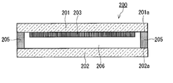
- FIG. 3A shows a plan view of the solar cell module according to the first comparative embodiment.
- FIG. 3B shows a cross-sectional view of the I-I chain line of the solar cell module shown in FIG. 3A.
- the solar cell module 200 according to the first comparative embodiment has a configuration in which the intermediate layer 104 is not provided in the solar cell module 100 according to the first embodiment.
- the first substrate 201, the peripheral edge portion 201a of the first substrate, the second substrate 202, the peripheral edge portion 202a of the second substrate, the solar cell 203, the first sealing layer 205, and the space 206 are the solar cell modules. It is the same as the first substrate 101, the peripheral edge portion 101a of the first substrate, the second substrate 102, the peripheral edge portion 102a of the second substrate, the solar cell 103, the first sealing layer 105, and the space 106 in 100, respectively. Therefore, detailed description thereof will be omitted here.
- the thickness of the first substrate 201 and the second substrate 202 in order to maintain the load bearing capacity.
- increasing the thickness of the first substrate 201 and the second substrate 202 causes disadvantages such as an increase in the total weight and an increase in light absorption loss in the substrate on the light receiving surface side (here, the first substrate 201).
- the solar cell module 100 according to the first embodiment can be manufactured by, for example, the following method.
- a manufacturing method when the solar cell 103 has the configuration shown in FIG. 2A will be described.
- the first electrode 107 is formed on the surface of the first substrate 101.
- an electron transport layer is formed on the first electrode 107 of the first substrate 101 by a sputtering method or the like.
- the photoelectric conversion layer 108 is formed on the electron transport layer by a coating method or the like.
- a hole transport layer is formed on the photoelectric conversion layer 108 by a coating method or the like.
- the second electrode 109 is formed on the hole transport layer by thin film deposition or the like.
- the solar cell 103 can be formed on the first substrate 101.
- the intermediate layer 104 is placed on the solar cell 103 provided on the first substrate 101 without being adhered to the solar cell 103.
- the second substrate 102 is arranged at a position facing the first substrate 101 with the solar cell 103 interposed therebetween, and a first sealing layer is further formed between the peripheral edge portion 101a of the first substrate 101 and the peripheral edge portion 102a of the second substrate 102. Place 105.
- a laminate composed of the first substrate 101, the solar cell 103, the intermediate layer 104, the first sealing layer 105, and the second substrate 102 can be obtained.
- the corner portion of the intermediate layer 104 is fixed to the first sealing layer 105, so that the position of the intermediate layer 104 is fixed.
- the laminate is integrated by integral molding such as heat pressure bonding, and at the same time, the peripheral edge portion is sealed by the first sealing layer 105. Thereby, the solar cell module 100 can be obtained.
- the first substrate 101 is arranged on the light receiving surface side of the solar cell module 100.
- the first substrate 101 has, for example, a water vapor barrier property and a translucent property.
- the first substrate 101 may be transparent. Further, the first substrate 101 plays a role of physically holding each layer constituting the solar cell 103 as a film when the solar cell module 100 is manufactured.
- An example of the first substrate 101 is a glass substrate or a plastic substrate.
- the plastic substrate may be a plastic film.
- the second substrate 102 is provided at a position facing the first substrate 101 of the solar cell module 100.
- the second substrate 102 has, for example, a water vapor barrier property.
- the second substrate 102 also serves to protect the solar cell 103.
- the second substrate 102 can suppress physical damage to the solar cell 103 due to an external factor such as sand particles.
- An example of the second substrate 102 is a glass substrate or a plastic substrate.
- the plastic substrate may be a plastic film.
- the second substrate 102 does not necessarily need to be translucent. Therefore, when the first substrate 101 itself has sufficient strength, or when the internal space is filled with the second sealing layer 110 or the like and has sufficient strength, an Al-deposited film or the like is used as the second substrate 102. Can be used.
- the electron transport layer includes, for example, a semiconductor.
- the electron transport layer may include a semiconductor having a band gap of 3.0 eV or more.
- a semiconductor having a band gap of 3.0 eV or more By forming the electron transport layer with a semiconductor having a band gap of 3.0 eV or more, visible light and infrared light can be transmitted to the photoelectric conversion layer 108.
- semiconductors are organic n-type semiconductors and inorganic n-type semiconductors.
- organic n-type semiconductors are imide compounds, quinone compounds, fullerenes, or derivatives of fullerenes.
- inorganic n-type semiconductors are metal oxides or perovskite oxides.
- metal oxides are Cd, Zn, In, Pb, Mo, W, Sb, Bi, Cu, Hg, Ti, Ag, Mn, Fe, V, Sn, Zr, Sr, Ga, Si, or Cr. It is an oxide.
- Specific examples include titanium oxide (ie, TiO 2 ).
- perovskite oxides are SrTIO 3 or CaTIO 3 .
- the photoelectric conversion layer 108 contains a perovskite compound.
- the perovskite compound is a structure having a perovskite crystal structure represented by the composition formula ABX 3 and a crystal similar thereto.
- A is a monovalent cation
- B is a divalent cation
- X is a monovalent anion.
- monovalent cations A are alkali metal cations or organic cations.
- Specific examples of the cation A is methyl ammonium cation (+ CH 3 NH 3), formamidinium cation (NH 2 CHNH 2 +), cesium cations (Cs +), or rubidium cation (Rb +).
- Examples of cation B are transition metals or divalent cations of Group 13 to Group 15 elements. Specific examples of cation B are Pb 2+ , Ge 2+ , or Sn 2+ .
- An example of anion X is a halogen anion. Each site of A, B, or X may be occupied by a plurality of types of ions.
- the photoelectric conversion layer 108 may be a perovskite compound having a structure similar to the perovskite structure represented by the composition formula ABX 3.
- An example of a similar structure is a structure in which a defect of a halogen anion is contained in a perovskite compound, or a structure in which a monovalent cation or a halogen anion is composed of a plurality of types of elements in a perovskite compound. be.
- the photoelectric conversion layer 108 may have a thickness of 100 nm or more and 1000 nm or less. The thickness of the photoelectric conversion layer 108 may depend on the magnitude of light absorption of the photoelectric conversion layer 108.
- the photoelectric conversion layer 108 can be formed by a solution coating method, a co-deposited method, or the like. Further, the photoelectric conversion layer 108 may have a form in which the photoelectric conversion layer 108 is partially mixed with the electron transport layer.
- the hole transport layer is composed of, for example, an organic semiconductor or an inorganic semiconductor.
- the hole transport layer may have a structure in which layers made of the same constituent materials are laminated, or may have a structure in which layers made of different materials are alternately laminated.
- organic semiconductors are polytriallylamine (PTAA), 2,2', 7,7'-tetrakis (N, N'-di-p-methoxyphenyllamine) -9-9'-spirobifluorene (Spiro-OMeTAD), or. It is poly (3,4-ethylenedioxythiophene) (PEDOT).
- An example of an inorganic semiconductor is a p-type inorganic semiconductor. Examples of p-type inorganic semiconductor is CuO, Cu 2 O, CuSCN, molybdenum oxide or nickel oxide.
- Intermediate layer 104 Details of the intermediate layer 104, such as the material used for the intermediate layer 104, are as described above.
- First Sealing Layer 105 Details of the first sealing layer 105, such as the material used for the first sealing layer 105, are as described above.
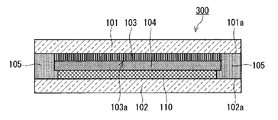
- FIG. 4A shows a plan view of the solar cell module according to the second embodiment.
- FIG. 4B shows a cross-sectional view of the I-I chain line of the solar cell module shown in FIG. 4A.
- FIG. 4C shows a cross-sectional view of the II-II chain line of the solar cell module shown in FIG. 4A.
- the solar cell module 300 shown in FIGS. 4A, 4B, and 4C has a configuration in which the solar cell module 100 according to the first embodiment includes a second sealing layer 110 instead of the space 106. Other than this, the solar cell module 300 has the same configuration as the solar cell module 100. From the viewpoint of moisture resistance and load capacity, it is desirable that the second sealing layer 110 is provided between the intermediate layer 104 and the second substrate 102 rather than the space 106. Since the second sealing layer 110 delays the diffusion rate of the moisture that has entered the module, the moisture resistance is improved. As a result, the durability of the solar cell module can be further improved.
- the softening temperature T3 of the material of the second sealing layer 110 is lower than the softening temperature T1 of the intermediate layer 104. Further, the perovskite solar cell 103 is relatively vulnerable to high temperatures. Therefore, it is desirable that the second sealing layer 110 can be softened at a lower temperature to seal between the first substrate 101 and the second substrate 102.
- the softening temperature T3 of the material of the second sealing layer 110 is preferably, for example, 150 ° C. or lower, and more preferably 130 ° C. or lower.
- the lower limit of the softening temperature T3 of the material of the second sealing layer 110 is not particularly limited. However, considering that the temperature of the solar cell module 300 in actual use can reach about 80 ° C., the softening temperature T3 is preferably 90 ° C. or higher, for example.
- the sealing temperature is the softening temperature T2 of the first sealing layer 105 and the softening temperature T3 of the second sealing layer 110. It is set to a temperature higher than the softening temperature of the higher of.
- An example of the material of the second sealing layer 110 is a polymer compound such as EVA or PO.
- the intermediate layer 104 is provided so as to be in contact with the main surface 103a of the solar cell 103, but is not fixed to the main surface 103a of the solar cell 103. That is, the position of the intermediate layer 104 is fixed in the solar cell module 300 so that the intermediate layer 104 is arranged in contact with the main surface 103a of the solar cell 103 without being fixed to the main surface 103a of the solar cell 103.
- the intermediate layer 104 may be fixed in position within the solar cell module 300 by fixing at least a portion of the peripheral edge of the intermediate layer 104 to the first sealing layer 105, as shown in FIG. 4C. ..
- the intermediate layer 104 may be fixed by the second substrate 102 or the second sealing layer 110. In this case, the intermediate layer 104 may be crimped by the second substrate 102 or the second sealing layer 110.
- the solar cell module 300 includes the intermediate layer 104, it has the same function and effect as the solar cell module 100 described in the first embodiment.
- the solar cell module 300 further has the effect of suppressing the peeling of the interface of each layer in the solar cell 103 by providing the intermediate layer 104 on the main surface 103a of the solar cell 103.
- the interface of each layer in the solar cell 103 is, for example, the interface between the photoelectric conversion layer 108 and the hole transport layer, the interface between the photoelectric conversion layer 108 and the electron transport layer, the interface between the hole transport layer and the second electrode 109, or the electron transport.
- the interface between the layer and the first electrode 107 This effect will be described in more detail.
- a heat crimping method is generally used.
- the material of the second sealing layer 110 is arranged between the first substrate 101 on which the solar cell 103 is provided and the second substrate 102 arranged so as to face the first substrate 101. ..
- the material of the first sealing layer 105 is arranged around the peripheral portion of the second sealing layer 110. In this way, a laminate composed of the first substrate 101, the solar cell 103, the intermediate layer 104, the first sealing layer 105, the second sealing layer 110, and the second substrate 102 can be obtained.
- the material of the second sealing layer 110 and the material of the first sealing layer 105 are softened by heating, and the entire laminate is pressure-bonded to obtain the first substrate 101, the solar cell 103, the intermediate layer 104, and the first. 2
- the sealing layer 110 and the second substrate 102 are integrated.
- the peripheral edge portion 101a of the first substrate 101 and the peripheral edge portion 102a of the second substrate 102 are integrated with the first sealing layer 105 and sealed.
- FIG. 5A shows a plan view of the solar cell module according to the second comparative embodiment.
- FIG. 5B shows a cross-sectional view of the I-I chain line of the solar cell module shown in FIG. 5A.
- the first substrate 201, the peripheral edge portion 201a of the first substrate, the second substrate 202, the peripheral edge portion 202a of the second substrate, the solar cell 203, the first sealing layer 205, and the second sealing layer are examples of the first substrate 201, the peripheral edge portion 201a of the first substrate, the second substrate 202, the peripheral edge portion 202a of the second substrate, the solar cell 203, the first sealing layer 205, and the second sealing layer.
- the 210 is a first substrate 101 in the solar cell module 300, a peripheral portion 101a of the first substrate, a second substrate 102, a peripheral portion 102a of the second substrate, a solar cell 103, a first sealing layer 105, and a second sealing. It is the same as the layer 110. Therefore, detailed description thereof will be omitted here.
- the main surface 203a of the solar cell 203 is in contact with the second sealing layer 210 as in the solar cell module 400 according to the second comparative embodiment, when the material of the second sealing layer 210 is heated and softened to crimp the laminate.
- peeling may occur at the interface where the bonding force between the layers is weak due to reasons such as being dragged by the flow of the material of the second sealing layer 210.
- the interface is the interface between the photoelectric conversion layer 208 and the hole transport layer, the interface between the photoelectric conversion layer 208 and the electron transport layer, the interface between the hole transport layer and the second electrode 209, or the interface between the electron transport layer and the first electrode 207. Is.
- an intermediate layer 104 is provided between the main surface 103a of the solar cell 103 and the second sealing layer 110.
- the intermediate layer 104 is made of a material having a softening temperature higher than that of the first sealing layer 105 and the second sealing layer 110. Therefore, even when the laminate is pressure-bonded while the material of the second sealing layer 110 is heated and softened, the intermediate layer 104 is interposed between the main surface 103a of the solar cell 103 and the second sealing layer 110. .. As a result, delamination of the solar cell 103 caused by being dragged by the flow of the second sealing layer 110 is suppressed.
- the desorbed gas is a desorbed gas derived from the material constituting the solar cell 103.
- the desorbed gas can diffuse, for example, into the entire second sealing layer 110.
- FIG. 6A shows a plan view of the solar cell module according to the third comparative embodiment.
- FIG. 6B shows a cross-sectional view of the I-I chain line of the solar cell module shown in FIG. 6A.
- the solar cell module 500 according to the third comparative embodiment has a configuration in which the solar cell module 400 according to the second comparative embodiment further includes an intermediate layer 211 formed on the main surface 203a of the solar cell 203 by a vapor deposition method. That is, the solar cell module 500 according to the third comparative embodiment is different from the solar cell module 300 according to the second embodiment in that the intermediate layer is fixed on the main surface of the solar cell.
- the intermediate layer 211 is fixed on the main surface 103a of the solar cell 203. Therefore, in the solar cell module 500, the movement of gas molecules is hindered at the interface between the intermediate layer 211 and the solar cell 203. As a result, the desorbed gas generated from the solar cell 203 can stay at a high concentration between the solar cell 203 and the intermediate layer 211. As a result, the characteristics of the solar cell deteriorate.
- the solar cell module 300 according to the second embodiment is provided with the improvement of the mechanical strength of the solar cell module 300 in addition to the improvement of the mechanical strength of the solar cell module 300. It can also have the effects of suppressing interfacial peeling between the layers of the multilayer structure constituting the solar cell 103, suppressing deterioration due to the retention of desorbed gas on the surface of the solar cell, and withstanding the load of the lightweight module.
- the solar cell module 300 according to the second embodiment can have high durability.
- the solar cell module 300 can be manufactured by, for example, the following method.
- the method of forming the solar cell 103 on the first substrate 101 is the same as that of the solar cell module 100 of the first embodiment.
- the intermediate layer 104 is placed on the solar cell 103 provided on the first substrate 101 without being adhered to the solar cell 103.
- the second substrate 102 is arranged at a position facing the first substrate 101 with the solar cell 103 interposed therebetween, the second sealing layer 110 is arranged between the intermediate layer 104 and the second substrate 102, and the first substrate is further arranged.
- the first sealing layer 105 is arranged between the peripheral edge portion 101a of the 101 and the peripheral edge portion 102a of the second substrate 102.
- the laminate is integrated by integral molding such as heat pressure bonding, and at the same time, the peripheral portion is further sealed between the first substrate 101 and the second substrate 102 by the first sealing layer 105 and the second sealing layer 110. do. Thereby, the solar cell module 300 can be obtained.
- the solar cell modules of Examples 1 to 4 and Comparative Examples 1 to 4 were produced, and the characteristics of these solar cell modules were evaluated.
- Example 1 The solar cell module of Example 1 has the same structure as the solar cell module 100 shown in FIGS. 1A, 1B, and 1C. The materials, sizes, and thicknesses of each component in the solar cell module of Example 1 are shown below.
- First substrate 101 Fluorine-doped SnO glass substrate with two layers (Nippon Sheet Glass Co., Ltd., thickness 0.7 mm, surface resistance 10 ⁇ / sq.) -Electron transport layer: Titanium oxide (thickness 30 nm), porous titanium oxide (thickness 200 nm) Photoelectric conversion layer 108: perovskite compound (thickness 300 nm) -Hole transport layer: PTAA (manufactured by Aldrich) Second substrate 102: Glass substrate (thickness 0.7 mm) First sealing layer 105: Butyl rubber (thickness 0.8 mm) Intermediate layer 104: glass substrate (softening temperature T1: over 450 ° C, thickness 0.5 mm)
- the method for manufacturing the solar cell module of Example 1 is as follows.
- a conductive glass substrate having a thickness of 0.7 mm and having two layers of fluorine-doped SnO on the main surface was prepared. This was used as the first substrate 101.
- the fluorine-doped SnO 2 layer in this conductive glass substrate was used as the first electrode 107.
- a titanium oxide layer having a thickness of about 30 nm and a porous titanium oxide layer having a thickness of 0.2 ⁇ m were formed as electron transport layers.
- the titanium oxide layer was formed on the first electrode 107 of the first substrate 101 by a sputtering method.
- the porous titanium oxide layer was formed by applying a titanium oxide paste on the titanium oxide layer, drying the layer, and firing the dried film at 500 ° C. for 30 minutes in the air.
- the titanium oxide paste was prepared by dispersing high-purity titanium oxide powder having an average primary particle size of 20 nm in ethyl cellulose.
- the raw material solution of the photoelectric conversion material was applied onto the electron transport layer by spin coating to form the photoelectric conversion layer 108 containing the perovskite compound.
- the raw material solution was 0.92 mol / L lead iodide (II) (manufactured by Tokyo Kasei Kogyo), 0.17 mol / L lead bromide (II) (manufactured by Tokyo Kasei Kogyo), and 0.83 mol / L iodine.
- Formamidinium bromide (manufactured by GreatCell Solar), 0.17 mol / L methylammonium bromide (manufactured by GreatCell Solar), 0.05 mol / L cesium iodide (manufactured by Iwatani Sangyo), and 0.05 mol / L iodide It was a solution containing rubidium (manufactured by Iwatani Sangyo). The solvent of the solution was a mixture of dimethyl sulfoxide (manufactured by across) and N, N-dimethylformamide (manufactured by across).
- the mixing ratio (DMSO: DMF) of dimethyl sulfoxide (DMSO) and N, N-dimethylformamide (DMF) in the raw material solution was 1: 4 (volume ratio). Then, the formed coating film was heat-treated on a hot plate at 115 ° C. for 15 minutes and 100 ° C. for 30 minutes to obtain a layer having a perovskite structure, which is a photoelectric conversion layer 108.
- DMSO dimethyl sulfoxide
- DMF N, N-dimethylformamide
- a toluene solution containing PTAA at a concentration of 10 mg / mL, lithium bis (fluorosulfonyl) imide (LiTFSI) at a concentration of 5 mmol / L, and tert-butylpyridine (tBP) at a concentration of 6 ⁇ L / mL was spin-coated on the photoelectric conversion layer 108.
- LiTFSI lithium bis (fluorosulfonyl) imide
- tBP tert-butylpyridine
- Gold was deposited at 150 nm on the hole transport layer as the second electrode 109.
- the solar cell 103 was formed on the first substrate 101.
- a glass substrate having a thickness of 0.5 mm as an intermediate layer 104 was placed on the solar cell 103 provided on the first substrate 101 without being adhered to the solar cell 103.
- a glass substrate having a thickness of 0.7 mm is arranged at a position facing the first substrate 101 with the solar cell 103 interposed therebetween, and further, the peripheral edge portion 101a of the first substrate 101 and the peripheral edge portion 102a of the second substrate 102.
- the first sealing layer 105 was placed between the two. As a result, a laminate composed of the first substrate 101, the solar cell 103, the intermediate layer 104, the first sealing layer 105, and the second substrate 102 was obtained.
- the position of the intermediate layer 104 was fixed by fixing the corner portion of the intermediate layer 104 to the first sealing layer 105.
- the laminated body was heat-bonded by a vacuum laminating method to obtain a solar cell module 100.
- the heating temperature (that is, the sealing temperature) at the time of pressure crimping was 120 ° C.
- the pressure crimping was carried out at 120 ° C. by degassing in 180 seconds and pressurizing the laminate in the lamination direction at 20 MPa in 300 seconds.
- the second sealing layer 110 is placed between the intermediate layer 104 arranged on the solar cell 103 provided on the first substrate 101 without adhesion and the second substrate 102.
- the solar cell module of Example 2 was produced by further arranging PO.
- the softening temperature of PO was 90 ° C.
- Example 3 In the solar cell module of Example 2, EVA was arranged instead of PO as the second sealing layer 110, and the solar cell module of Example 3 was produced. Since the softening temperature of EVA is 130 ° C., pressure crimping was performed at 130 ° C.
- Example 4 In the solar cell module of Example 2, a polyethylene plate (softening temperature T1: 140 ° C.) having a thickness of 0.5 mm was arranged as the intermediate layer 104 instead of the glass plate to produce the solar cell module of Example 4.
- the characteristics and moisture resistance of the solar cell module before and after sealing were evaluated.
- the characteristics of the solar cell module are as follows: the solar cell module is irradiated with light having an illuminance of 100 mW / cm 2 using a halogen lamp (“BPS X300BA” manufactured by Spectrometer Co., Ltd.), and the stabilized current-voltage characteristic is BAS.
- BPS X300BA halogen lamp
- the measurement was performed using "ALS440B” manufactured by ALS 440B Co., Ltd. As a result, the conversion efficiency of each solar cell module was obtained.
- the maintenance rate after sealing is a relative value of the conversion efficiency after sealing when the conversion efficiency before sealing is 100. It was judged that the maintenance rate after sealing was 95% or more and the effect was sufficient, and the maintenance rate after 99% or more was sufficient.
- the maintenance rate after the moisture resistance test is a relative value of the conversion efficiency after the moisture resistance test when the conversion efficiency before the moisture resistance test is 100. It was judged that the maintenance rate after the moisture resistance test was 95% or more, which was effective, and 99% or more, which was sufficient.
- the load capacity evaluation was judged by the presence or absence of visual cracking or deformation after pressure crimping in module fabrication.
- the retention rate after sealing was lower than 95%.
- the solar cell module of Comparative Example 4 In the solar cell module of Comparative Example 4, no interfacial peeling of the solar cell 103 was observed. However, since the intermediate layer 104 is fixed to the solar cell 103, it is considered that the desorbed gas from the solar cell 103 is affected by the retention at a high concentration.
- the diffusion of the moisture infiltrated into the module is suppressed by introducing the second sealing layer 110 with respect to the solar cell module of the first embodiment, which is sufficient for improving the maintenance rate after the moisture resistance test.
- the effect was obtained.
- the same effect was expected in the solar cell module of Example 3, but the maintenance rate after the moisture resistance test was the same as that of Example 1.
- it is probable that the solar cell 103 was slightly damaged as compared with Example 2 due to the increase in the sealing temperature due to the increase in the softening point of the second sealing layer 110.
- Example 4 in which a polyethylene plate was used showed the same maintenance rate after the moisture resistance test as in Example 2 while being lighter.
- Example 1 using the intermediate layer 104 with respect to the solar cell module of Comparative Example 1, deformation was suppressed and substrate cracking did not occur. Since the solar cell modules of Examples 2 to 4 used the second sealing layer 110 and also used the intermediate layer 104, there was no cracking or deformation.
- the solar cell module of the present disclosure is widely used as a device for a power generation system that converts sunlight into electricity.
Landscapes
- Chemical & Material Sciences (AREA)
- Chemical Kinetics & Catalysis (AREA)
- Electrochemistry (AREA)
- Engineering & Computer Science (AREA)
- Power Engineering (AREA)
- Microelectronics & Electronic Packaging (AREA)
- Physics & Mathematics (AREA)
- Electromagnetism (AREA)
- Photovoltaic Devices (AREA)
Priority Applications (4)
| Application Number | Priority Date | Filing Date | Title |
|---|---|---|---|
| JP2022530071A JPWO2021251048A1 (https=) | 2020-06-11 | 2021-05-12 | |
| CN202180035853.7A CN115668515A (zh) | 2020-06-11 | 2021-05-12 | 太阳能电池模块 |
| EP21821295.9A EP4167306A4 (en) | 2020-06-11 | 2021-05-12 | SOLAR CELL MODULE |
| US18/055,407 US20230083628A1 (en) | 2020-06-11 | 2022-11-14 | Solar cell module |
Applications Claiming Priority (2)
| Application Number | Priority Date | Filing Date | Title |
|---|---|---|---|
| JP2020101919 | 2020-06-11 | ||
| JP2020-101919 | 2020-06-11 |
Related Child Applications (1)
| Application Number | Title | Priority Date | Filing Date |
|---|---|---|---|
| US18/055,407 Continuation US20230083628A1 (en) | 2020-06-11 | 2022-11-14 | Solar cell module |
Publications (1)
| Publication Number | Publication Date |
|---|---|
| WO2021251048A1 true WO2021251048A1 (ja) | 2021-12-16 |
Family
ID=78845959
Family Applications (1)
| Application Number | Title | Priority Date | Filing Date |
|---|---|---|---|
| PCT/JP2021/017968 Ceased WO2021251048A1 (ja) | 2020-06-11 | 2021-05-12 | 太陽電池モジュール |
Country Status (5)
| Country | Link |
|---|---|
| US (1) | US20230083628A1 (https=) |
| EP (1) | EP4167306A4 (https=) |
| JP (1) | JPWO2021251048A1 (https=) |
| CN (1) | CN115668515A (https=) |
| WO (1) | WO2021251048A1 (https=) |
Cited By (1)
| Publication number | Priority date | Publication date | Assignee | Title |
|---|---|---|---|---|
| WO2025197513A1 (ja) * | 2024-03-22 | 2025-09-25 | 株式会社カネカ | 太陽電池モジュール |
Families Citing this family (1)
| Publication number | Priority date | Publication date | Assignee | Title |
|---|---|---|---|---|
| KR20230023108A (ko) * | 2021-08-09 | 2023-02-17 | 삼성디스플레이 주식회사 | 표시 장치 |
Citations (7)
| Publication number | Priority date | Publication date | Assignee | Title |
|---|---|---|---|---|
| JP2005159181A (ja) * | 2003-11-27 | 2005-06-16 | Kyocera Corp | 太陽電池モジュールの製造方法 |
| JP2016157777A (ja) * | 2015-02-24 | 2016-09-01 | 株式会社東芝 | 太陽電池とその製造方法 |
| JP2017168500A (ja) * | 2016-03-14 | 2017-09-21 | 株式会社カネカ | 積層型光電変換装置およびその製造方法 |
| US20190006547A1 (en) * | 2015-12-14 | 2019-01-03 | Oxford Photovoltaics Limited | Photovoltaic module encapsulation |
| WO2019087918A1 (ja) * | 2017-10-31 | 2019-05-09 | 京セラ株式会社 | 太陽電池モジュール |
| JP2019071406A (ja) * | 2017-02-16 | 2019-05-09 | パナソニックIpマネジメント株式会社 | 太陽電池モジュール |
| CN111261785A (zh) * | 2020-03-26 | 2020-06-09 | 中国科学院上海硅酸盐研究所 | 钙钛矿太阳能电池组件及其封装方法 |
Family Cites Families (19)
| Publication number | Priority date | Publication date | Assignee | Title |
|---|---|---|---|---|
| JPS61280677A (ja) * | 1985-06-06 | 1986-12-11 | Matsushita Electric Ind Co Ltd | 太陽電池モジユ−ル |
| JPS6286875A (ja) * | 1985-10-14 | 1987-04-21 | Matsushita Electric Ind Co Ltd | 太陽電池モジユ−ル |
| JPS6392064A (ja) * | 1986-10-07 | 1988-04-22 | Matsushita Electric Ind Co Ltd | 太陽電池モジユ−ル |
| JP2002083978A (ja) * | 2000-09-05 | 2002-03-22 | Sanyo Electric Co Ltd | 太陽電池モジュールの製造方法 |
| JP4076742B2 (ja) * | 2001-07-13 | 2008-04-16 | シャープ株式会社 | 太陽電池モジュール |
| JP4051430B2 (ja) * | 2001-11-06 | 2008-02-27 | 独立行政法人産業技術総合研究所 | リサイクル対応型太陽電池モジュール |
| JP2004288677A (ja) * | 2003-03-19 | 2004-10-14 | Sharp Corp | 太陽電池モジュールサブアセンブリおよび複層ガラス型太陽電池モジュール |
| JP4550390B2 (ja) * | 2003-09-22 | 2010-09-22 | 積水樹脂株式会社 | 太陽電池モジュール |
| JP2006179626A (ja) * | 2004-12-22 | 2006-07-06 | Showa Shell Sekiyu Kk | Cis系薄膜太陽電池モジュール、該太陽電池モジュールの製造方法及び分離方法 |
| JP2009033130A (ja) * | 2007-06-28 | 2009-02-12 | Kyocera Corp | 太陽電池モジュール及び太陽電池モジュールの製造方法 |
| US20090203283A1 (en) * | 2008-02-07 | 2009-08-13 | Margaret Helen Gentile | Method for sealing an electronic device |
| JP2009224757A (ja) * | 2008-02-22 | 2009-10-01 | Kyocera Corp | 光電変換装置 |
| KR101028228B1 (ko) * | 2009-10-28 | 2011-04-11 | 엘지이노텍 주식회사 | 태양광 발전장치 |
| JP2011151195A (ja) * | 2010-01-21 | 2011-08-04 | Dainippon Printing Co Ltd | 有機薄膜太陽電池およびその製造方法 |
| JP2012080060A (ja) * | 2010-09-07 | 2012-04-19 | Mitsubishi Chemicals Corp | 有機太陽電池モジュール |
| JP5662838B2 (ja) * | 2011-02-24 | 2015-02-04 | 本田技研工業株式会社 | 太陽電池モジュール |
| WO2014136359A1 (ja) * | 2013-03-07 | 2014-09-12 | ローム株式会社 | 有機薄膜太陽電池およびその製造方法、および電子機器 |
| WO2014136969A1 (ja) * | 2013-03-08 | 2014-09-12 | コニカミノルタ株式会社 | 有機エレクトロルミネッセンス素子、及び、有機エレクトロルミネッセンス素子の製造方法 |
| JP6030176B2 (ja) * | 2015-03-19 | 2016-11-24 | 株式会社東芝 | 光電変換素子とその製造方法 |
-
2021
- 2021-05-12 EP EP21821295.9A patent/EP4167306A4/en active Pending
- 2021-05-12 WO PCT/JP2021/017968 patent/WO2021251048A1/ja not_active Ceased
- 2021-05-12 CN CN202180035853.7A patent/CN115668515A/zh active Pending
- 2021-05-12 JP JP2022530071A patent/JPWO2021251048A1/ja active Pending
-
2022
- 2022-11-14 US US18/055,407 patent/US20230083628A1/en not_active Abandoned
Patent Citations (7)
| Publication number | Priority date | Publication date | Assignee | Title |
|---|---|---|---|---|
| JP2005159181A (ja) * | 2003-11-27 | 2005-06-16 | Kyocera Corp | 太陽電池モジュールの製造方法 |
| JP2016157777A (ja) * | 2015-02-24 | 2016-09-01 | 株式会社東芝 | 太陽電池とその製造方法 |
| US20190006547A1 (en) * | 2015-12-14 | 2019-01-03 | Oxford Photovoltaics Limited | Photovoltaic module encapsulation |
| JP2017168500A (ja) * | 2016-03-14 | 2017-09-21 | 株式会社カネカ | 積層型光電変換装置およびその製造方法 |
| JP2019071406A (ja) * | 2017-02-16 | 2019-05-09 | パナソニックIpマネジメント株式会社 | 太陽電池モジュール |
| WO2019087918A1 (ja) * | 2017-10-31 | 2019-05-09 | 京セラ株式会社 | 太陽電池モジュール |
| CN111261785A (zh) * | 2020-03-26 | 2020-06-09 | 中国科学院上海硅酸盐研究所 | 钙钛矿太阳能电池组件及其封装方法 |
Non-Patent Citations (3)
| Title |
|---|
| JULIAN BURCHCKA, NATURE, vol. 499, July 2013 (2013-07-01), pages 316 - 319 |
| See also references of EP4167306A4 |
| WEI CHEN, SCIENCE, vol. 350, no. 6263, November 2015 (2015-11-01), pages 944 - 948 |
Cited By (1)
| Publication number | Priority date | Publication date | Assignee | Title |
|---|---|---|---|---|
| WO2025197513A1 (ja) * | 2024-03-22 | 2025-09-25 | 株式会社カネカ | 太陽電池モジュール |
Also Published As
| Publication number | Publication date |
|---|---|
| US20230083628A1 (en) | 2023-03-16 |
| CN115668515A (zh) | 2023-01-31 |
| EP4167306A1 (en) | 2023-04-19 |
| JPWO2021251048A1 (https=) | 2021-12-16 |
| EP4167306A4 (en) | 2023-12-06 |
Similar Documents
| Publication | Publication Date | Title |
|---|---|---|
| US6239355B1 (en) | Solid-state photoelectric device | |
| JP5612658B2 (ja) | 光電子デバイス | |
| WO2005106968A1 (ja) | カルコパイライト型太陽電池 | |
| JP7390668B2 (ja) | 太陽電池モジュール | |
| JP6554300B2 (ja) | 光電変換装置の製造方法 | |
| WO2020246074A1 (ja) | 4端子タンデム太陽電池 | |
| CN114270540A (zh) | 多结光伏器件 | |
| WO2021220925A1 (ja) | 太陽電池 | |
| US20230083628A1 (en) | Solar cell module | |
| CN102568867A (zh) | 一种叠层薄膜太阳能电池 | |
| CN117355156A (zh) | 光伏器件及其制作方法 | |
| TWI596791B (zh) | 太陽能電池模組 | |
| JP2026004326A (ja) | 光電変換モジュール | |
| WO2025175859A1 (zh) | 一种钙钛矿太阳能电池组件封装结构及其封装方法 | |
| US20220077412A1 (en) | Solar cell module | |
| CN118510299A (zh) | 叠层电池及其制备方法 | |
| CN118765120A (zh) | 一种封装的钙钛矿太阳能电池组件及制备方法 | |
| CN117650186A (zh) | 光伏器件及其封装方法 | |
| JP7631573B1 (ja) | 太陽電池モジュールおよび太陽電池モジュールの製造方法 | |
| CN108376720A (zh) | 一种光伏电池组件及其制作方法 | |
| WO2022009636A1 (ja) | 太陽電池および光電変換素子 | |
| KR102896485B1 (ko) | 페로브스카이트 태양전지 모듈 및 그의 제조방법 | |
| WO2025173743A1 (ja) | フレキシブル太陽電池 | |
| CN121398350A (zh) | 一种太阳电池及其制备方法、光伏组件 | |
| WO2026076037A1 (en) | Construction of solar modules to extend lifecycles of perovskite solar cells contained therein |
Legal Events
| Date | Code | Title | Description |
|---|---|---|---|
| 121 | Ep: the epo has been informed by wipo that ep was designated in this application |
Ref document number: 21821295 Country of ref document: EP Kind code of ref document: A1 |
|
| ENP | Entry into the national phase |
Ref document number: 2022530071 Country of ref document: JP Kind code of ref document: A |
|
| NENP | Non-entry into the national phase |
Ref country code: DE |
|
| ENP | Entry into the national phase |
Ref document number: 2021821295 Country of ref document: EP Effective date: 20230111 |