WO2021250870A1 - 増幅回路、差動増幅回路、受信回路及び半導体集積回路 - Google Patents
増幅回路、差動増幅回路、受信回路及び半導体集積回路 Download PDFInfo
- Publication number
- WO2021250870A1 WO2021250870A1 PCT/JP2020/023110 JP2020023110W WO2021250870A1 WO 2021250870 A1 WO2021250870 A1 WO 2021250870A1 JP 2020023110 W JP2020023110 W JP 2020023110W WO 2021250870 A1 WO2021250870 A1 WO 2021250870A1
- Authority
- WO
- WIPO (PCT)
- Prior art keywords
- transistor
- circuit
- input
- node
- gate electrode
- Prior art date
- Legal status (The legal status is an assumption and is not a legal conclusion. Google has not performed a legal analysis and makes no representation as to the accuracy of the status listed.)
- Ceased
Links
Images







Classifications
-
- H—ELECTRICITY
- H03—ELECTRONIC CIRCUITRY
- H03F—AMPLIFIERS
- H03F3/00—Amplifiers with only discharge tubes or only semiconductor devices as amplifying elements
- H03F3/45—Differential amplifiers
- H03F3/45071—Differential amplifiers with semiconductor devices only
- H03F3/45076—Differential amplifiers with semiconductor devices only characterised by the way of implementation of the active amplifying circuit in the differential amplifier
- H03F3/45179—Differential amplifiers with semiconductor devices only characterised by the way of implementation of the active amplifying circuit in the differential amplifier using MOSFET transistors as the active amplifying circuit
- H03F3/45273—Mirror types
-
- G—PHYSICS
- G05—CONTROLLING; REGULATING
- G05F—SYSTEMS FOR REGULATING ELECTRIC OR MAGNETIC VARIABLES
- G05F3/00—Non-retroactive systems for regulating electric variables by using an uncontrolled element, or an uncontrolled combination of elements, such element or such combination having self-regulating properties
- G05F3/02—Regulating voltage or current
- G05F3/08—Regulating voltage or current wherein the variable is DC
- G05F3/10—Regulating voltage or current wherein the variable is DC using uncontrolled devices with non-linear characteristics
- G05F3/16—Regulating voltage or current wherein the variable is DC using uncontrolled devices with non-linear characteristics being semiconductor devices
- G05F3/20—Regulating voltage or current wherein the variable is DC using uncontrolled devices with non-linear characteristics being semiconductor devices using diode- transistor combinations
- G05F3/26—Current mirrors
- G05F3/262—Current mirrors using field-effect transistors only
-
- H—ELECTRICITY
- H03—ELECTRONIC CIRCUITRY
- H03F—AMPLIFIERS
- H03F1/00—Details of amplifiers with only discharge tubes, only semiconductor devices or only unspecified devices as amplifying elements
- H03F1/08—Modifications of amplifiers to reduce detrimental influences of internal impedances of amplifying elements
- H03F1/083—Modifications of amplifiers to reduce detrimental influences of internal impedances of amplifying elements in transistor amplifiers
- H03F1/086—Modifications of amplifiers to reduce detrimental influences of internal impedances of amplifying elements in transistor amplifiers with FET's
-
- H—ELECTRICITY
- H03—ELECTRONIC CIRCUITRY
- H03F—AMPLIFIERS
- H03F3/00—Amplifiers with only discharge tubes or only semiconductor devices as amplifying elements
- H03F3/34—DC amplifiers in which all stages are DC-coupled
- H03F3/343—DC amplifiers in which all stages are DC-coupled with semiconductor devices only
- H03F3/347—DC amplifiers in which all stages are DC-coupled with semiconductor devices only in integrated circuits
-
- H—ELECTRICITY
- H03—ELECTRONIC CIRCUITRY
- H03F—AMPLIFIERS
- H03F3/00—Amplifiers with only discharge tubes or only semiconductor devices as amplifying elements
- H03F3/45—Differential amplifiers
- H03F3/45071—Differential amplifiers with semiconductor devices only
- H03F3/45076—Differential amplifiers with semiconductor devices only characterised by the way of implementation of the active amplifying circuit in the differential amplifier
- H03F3/45179—Differential amplifiers with semiconductor devices only characterised by the way of implementation of the active amplifying circuit in the differential amplifier using MOSFET transistors as the active amplifying circuit
- H03F3/45183—Long tailed pairs
-
- H—ELECTRICITY
- H03—ELECTRONIC CIRCUITRY
- H03F—AMPLIFIERS
- H03F3/00—Amplifiers with only discharge tubes or only semiconductor devices as amplifying elements
- H03F3/45—Differential amplifiers
- H03F3/45071—Differential amplifiers with semiconductor devices only
- H03F3/45076—Differential amplifiers with semiconductor devices only characterised by the way of implementation of the active amplifying circuit in the differential amplifier
- H03F3/45475—Differential amplifiers with semiconductor devices only characterised by the way of implementation of the active amplifying circuit in the differential amplifier using IC blocks as the active amplifying circuit
-
- H—ELECTRICITY
- H03—ELECTRONIC CIRCUITRY
- H03F—AMPLIFIERS
- H03F2200/00—Indexing scheme relating to amplifiers
- H03F2200/474—A current mirror being used as sensor
Definitions
- One embodiment disclosed in the present specification and the like relates to, for example, an amplifier circuit, a differential amplifier circuit, a receiver circuit, and a semiconductor integrated circuit used in a CTLE (Continuous Time Liner Equalizer, continuous time linear equalizer).
- CTLE Continuous Time Liner Equalizer, continuous time linear equalizer
- CTLE is an input amplifier circuit of a SerDes (SERializer DESerializer) receiving circuit used for a high-speed interface for a network or a data center, and is used as a loss compensation circuit in a transmission line.
- the conventional CTLE uses a source degeneration type equalizer.
- the conventional CTLE using the source degeneration type equalizer realizes the boost gain amplification function by using the inductor element (coil). Therefore, the circuit size (area) becomes large. In addition, the gain becomes non-linear due to variation factors such as resistance and mutual conductance in the circuit.
- One of the problems to be solved by the embodiments disclosed in the present specification and the like is an amplifier circuit, a differential amplifier circuit, and a receiving circuit that realize a boost gain amplification function and a small area while maintaining the linearity of the gain. And to provide semiconductor integrated circuits.
- the amplifier circuit includes a first circuit including a first transistor connected between an input node through which an input current flows and a reference potential node, and a gate electrode connected to the input node, and a low-pass filter circuit.
- a second circuit including a second transistor connected in parallel with the first transistor between the input node and the reference potential node and having a gate electrode connected to the gate of the first transistor via the low pass filter circuit. It has a third circuit including a third transistor connected between the output node through which the output current flows and the reference potential node and the gate electrode connected to the gate of the first transistor.
- an amplifier circuit, a differential amplifier circuit, a receiver circuit, and a semiconductor integrated circuit that realize a boost gain amplification function and a small area while maintaining gain linearity are realized. be able to.
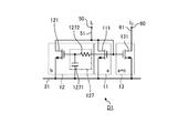
- FIG. 1 is a diagram showing a configuration of an amplifier circuit according to the first embodiment.
- FIG. 2 is a diagram showing the relationship between the DC gain, boost gain, peak gain and frequency of the amplifier circuit according to the first embodiment.
- FIG. 3 is a diagram showing a configuration of an amplifier circuit according to a second embodiment.
- FIG. 4 is a diagram showing the relationship between the DC gain, boost gain, peak gain and frequency of the amplifier circuit according to the second embodiment.
- FIG. 5 is a diagram showing a configuration of an amplifier circuit according to a third embodiment.
- FIG. 6 is a diagram showing the relationship between the DC gain, boost gain, peak gain and frequency of the amplifier circuit according to the third embodiment.
- FIG. 7 is a diagram showing a configuration of an amplifier circuit according to a fourth embodiment.
- FIG. 1 is a diagram showing a configuration of an amplifier circuit according to the first embodiment.
- FIG. 2 is a diagram showing the relationship between the DC gain, boost gain, peak gain and frequency of the amplifier circuit according to the first embodiment.
- FIG. 8 is a diagram showing a configuration of an amplifier circuit according to a fifth embodiment.
- FIGS. 9A, 9B, and 9C is a look-up table for determining the size parameter based on the DC gain and the boost gain.
- FIG. 10 is a diagram showing a configuration of an amplifier circuit according to a sixth embodiment.
- FIG. 11 is a diagram showing the configuration of the receiving circuit according to the seventh embodiment.
- FIG. 12 is a diagram showing the configuration of the semiconductor integrated circuit according to the eighth embodiment.
- FIG. 1 is a diagram showing a configuration of an amplifier circuit D1 according to the first embodiment.
- the amplifier circuit D1 is a single-ended amplifier.
- the amplifier circuit D1 includes a first circuit 11, a second circuit 12, a third circuit 13, a reference potential node 31, an input terminal 50, an input node 51, an output terminal 60, and an output node 61. ..
- a and b are parameters indicating the magnitude of the current flowing through the transistors of the first circuit 11 and the second circuit 12, respectively, and are parameters indicating the size of the transistor (hereinafter, referred to as “size parameter”). Call.).
- the size parameters a and b correspond to, for example, the number of fins of a FinFET (Fin Field Effect Transistor) and the gate width of a planar type transistor.
- the input node 51 includes wiring through which the input current I I flows.
- the output node 61 includes wiring through which the output current IO flows.
- the reference potential node 31 includes wiring to which the reference potential Vbase (for example, the ground potential) is supplied.
- the potential Vin of the input node 51 and the reference potential Vbase have a relationship of Vin> Vbase.
- the first circuit 11 has a first transistor 111.
- the first transistor 111 is, for example, an n-channel transistor, and is connected between the input node 51 through which the input current I I flows and the reference potential node 31.
- the gate electrode of the first transistor 111 is connected to the input node 51. Further, the drain electrode and the source electrode of the first transistor 111 are connected to the input node 51 and the reference potential node 31, respectively.
- the size parameter of the first transistor 111 is a.
- the first transistor 111 is an example of the first transistor.
- the second circuit 12 has a second transistor 121 and a low-pass filter circuit 127.
- the second transistor 121 is, for example, an n-channel transistor, and is connected in parallel with the first transistor 111 between the input node 51 through which the input current I I flows and the reference potential node 31.
- the gate electrode of the second transistor 121 is connected to the gate electrode of the first transistor 111 via a low-pass filter circuit 127. Further, the drain electrode and the source electrode of the second transistor 121 are connected to the input node 51 and the reference potential node 31, respectively.
- the size parameter of the second transistor 121 is b.
- the second transistor 121 is an example of the second transistor.
- the low-pass filter circuit 127 is a low-pass filter composed of a capacitor 1271 and a resistor 1272.
- the low-pass filter circuit 127 filters the signal to the gate electrode of the second transistor 121 in the high frequency band.
- the third circuit 13 has a third transistor 131.
- the third transistor 131 is, for example, an n-channel transistor, and is connected between the output node 61 through which the output current IO flows and the reference potential node 31.
- the gate electrode of the third transistor 131 is connected to the gate electrode of the first transistor 111.
- the size parameter of the third transistor 131 is a + b. That is, the size parameter a + b of the third transistor 131 is equal to the sum of the size parameter a of the first transistor 111 and the size parameter b of the second transistor 121.
- the third transistor 131 is an example of the third transistor.
- the first circuit 11 and the second circuit 12 form a current mirror circuit with the third circuit 13.
- the current I a + b at a ratio corresponding to the size parameter a + b of the third transistor 131 flows in the third circuit 13 at the mirror destination.
- FIG. 2 is a diagram showing the relationship between the DC gain, boost gain, peak gain and frequency of the amplifier circuit D1 according to the first embodiment.
- the DC gain corresponds to a gain that does not reflect the filtering operation of the low-pass filter circuit 127, and corresponds to a gain when the frequency of the input current I I is smaller than the cutoff frequency of the low-pass filter circuit 127.
- the peak gain corresponds to the gain reflecting the filtering operation of the low-pass filter circuit 127, and corresponds to the gain when the frequency of the input current I I is larger than the cutoff frequency of the low-pass filter circuit 127.
- a drain current I a + b flows through the third transistor 131 as a mirror current based on the current mirror operation.
- a current I a having a ratio corresponding to the size parameter a of the first transistor 111 flows through the first circuit 11.
- the gate electrode of the second transistor 121 is connected to the gate electrode of the first transistor 111 via the low-pass filter circuit 127.
- the gain (peak gain) when the frequency of the input current I I is larger than the cutoff frequency of the low-pass filter circuit 127 and the frequency of the input current I I are obtained from the cutoff frequency of the low-pass filter circuit 127.
- the difference from the gain (DC gain) when it is small can be determined according to the size parameter b of the second transistor 121.
- gm is the mutual conductance
- s is the variable of the Laplace transform
- CTOT is the value of the total capacity of the gate terminal.
- the amplifier circuit D1 includes the first circuit 11, the second circuit 12, and the third circuit 13.
- the first circuit 11 includes a first transistor 111 connected between an input node 51 through which an input current flows and a reference potential node 31 and having a gate electrode connected to the input node 51.
- the second circuit 12 includes a low-pass filter circuit 127.
- the second circuit 12 is connected in parallel with the first transistor 111 between the input node 51 and the reference potential node 31, and the gate electrode is connected to the gate electrode of the first transistor 111 via the low pass filter circuit 127.
- the third circuit 13 includes a third transistor 131 connected between the output node 61 through which the output current flows and the reference potential node 31 and having the gate electrode connected to the first transistor 111.
- the input signal input to the gate electrode of the second transistor 121 is filtered by the low-pass filter circuit 127. Therefore, in the high frequency band, it is possible to suppress the current I b from flowing through the second transistor 121, and the amplification factor can be increased from the DC gain to the peak gain.
- the amplifier circuit D1 does not require an inductor element (coil). Therefore, the circuit area can be reduced and the power consumption can be reduced as compared with the conventional amplifier circuit using the inductor element (coil).
- the amplifier circuit D1 is based on the current mirror circuit manufactured by the same process.
- input and output variation factors for example, parameters such as transistor threshold Vth and gain coefficient ⁇
- these variation factors cancel each other out due to the same change, and finally an amplifier circuit with a small gain error can be realized.
- the DC gain and the boost gain are varied by using a resistor (resistance value RS ), a capacitor (capacity CS ), an inductor parasitic resistance (resistance value RP ), and a load resistance (resistance value RL).
- the amplification factor A i of the amplifier circuit D1 which is based on current mirror circuit, as shown below, can be achieved linearity.
- I out ( ⁇ out / 2) V od 2 (3)
- the amplification factor A i of the amplifier circuit D1 is expressed by the following equation (5), the linear.
- a i ( ⁇ out / ⁇ in ) (5)
- FIG. 3 is a diagram showing the configuration of the amplifier circuit D2 according to the second embodiment.
- the amplifier circuit D2 includes, in addition to the configuration of the amplifier circuit D1 shown in FIG. 1, a constant current source 40 which outputs a current I c of the ratio corresponding to the size parameter c to the input node 51 side Have more.
- the constant current source 40 is connected in parallel with the first transistor 111 and the second transistor 121 between the input node 51 and the reference potential node 31.
- the size parameter of the third transistor 131 is a + b + c on the output node 61 side in response to the addition of the constant current source 40.
- FIG. 4 is a diagram showing the relationship between the DC gain, boost gain, peak gain and frequency of the amplifier circuit D2 according to the second embodiment. The operation of the amplifier circuit D2 will be described with reference to FIGS. 3 and 4.
- the third circuit 13, the first circuit 11, the second circuit 12, and the constant current source 40 operate as a current mirror circuit.
- the current I a + b + c at a ratio corresponding to the size parameter a + b + c of the third transistor 131 flows in the third circuit 13 at the mirror destination.
- the drain current I a + b + c flows through the third transistor 131 at the mirror destination based on the current mirror operation.
- a current I a having a ratio corresponding to the size parameter a of the first transistor 111 flows through the first circuit 11.
- the current I b does not flow in the second transistor 121.
- the amplifier circuit D2 according to the second embodiment, not only the boost gain but also the DC gain can be amplified. Further, by adjusting the current I c outputted by the constant current source 40, it is possible to amplify the boost gain and DC gain variably. Further, the boost gain can be further amplified as compared with the amplifier circuit D1 according to the first embodiment.
- FIG. 5 is a diagram showing the configuration of the amplifier circuit D3 according to the third embodiment.
- the amplifier circuit D3 is a differential amplifier that inputs input currents I IP and I IN from input terminals 50 and 52 and outputs output currents I OP and I ON from output terminals 60 and 62. be.
- the amplifier circuit D3 includes a first circuit 11, a second circuit 12, a third circuit 13, a fourth circuit 14, a fifth circuit 15, a sixth circuit 16, a seventh circuit 17, an eighth circuit 18, an input node 51, and a reference. It has a potential node 31 and an output node 61.
- the first circuit 11 and the second circuit 12 are as described in the first embodiment. Further, the size parameters of the third transistor 131 included in the third circuit 13 are the size parameter a of the first transistor 111, the size parameter b of the second transistor 121, and the size parameter c of the seventh transistor 171 included in the seventh circuit 17. Is equal to the sum of. That is, the size parameter of the third transistor 131 is a + b + c.
- the fourth circuit 14 has a fourth transistor 141.
- the fourth transistor 141 is, for example, an n-channel transistor, and is connected between the input node 32 through which the input current I IN flows and the reference potential node 31.
- the gate electrode of the fourth transistor 141 is connected to the input node 32.
- the drain electrode and the source electrode of the fourth transistor 141 are connected to the input node 32 and the reference potential node 31, respectively.
- the size parameter of the fourth transistor 141 is a.
- the fifth circuit 15 has a fifth transistor 151 and a low-pass filter circuit 157.
- the fifth transistor 151 is, for example, an n-channel transistor, and is connected in parallel with the fourth transistor 141 between the input node 32 through which the input current I IN flows and the reference potential node 31.
- the gate electrode of the fifth transistor 151 is connected to the fourth transistor 141 via a low-pass filter circuit 157. Further, the drain electrode and the source electrode of the fifth transistor 151 are connected to the input node 32 and the reference potential node 31, respectively.
- the size parameter of the fifth transistor 151 is b.
- the low-pass filter circuit 157 has a capacitor 1571 and a resistor 1572.
- the function of the low-pass filter circuit 157 is the same as that of the low-pass filter circuit 127.
- the sixth circuit 16 has a sixth transistor 161.
- the sixth transistor 161 is, for example, an n-channel transistor, and is connected between the output node 63 through which the output current ION flows and the reference potential node 31.
- the gate electrode of the sixth transistor 161 is connected to the gate electrode of the fourth transistor 141. Further, the drain electrode and the source electrode of the sixth transistor 161 are connected to the output node 63 and the reference potential node 31, respectively.
- the size parameter of the sixth transistor 161 is equal to the sum of the size parameter a of the fourth transistor 141, the size parameter b of the fifth transistor 151, and the size parameter c of the eighth transistor 181 of the eighth circuit 18. That is, the size parameter of the sixth transistor 161 is a + b + c.
- the seventh circuit 17 has a seventh transistor 171.
- the seventh transistor 171 is, for example, an n-channel transistor, and is connected between the input node 53 through which the input current I IN flows and the reference potential node 31. Further, the gate electrode of the 7th transistor 171 is connected to the gate electrode of the 1st transistor 111.
- the size parameter of the seventh transistor 171 is c.
- the eighth circuit 18 has an eighth transistor 181.
- the eighth transistor 181 is, for example, an n-channel transistor, and is connected between the input node 51 through which the input current IP flows and the reference potential node 31. Further, the gate electrode of the 8th transistor 181 is connected to the gate electrode of the 4th transistor 141.
- the size parameter of the eighth transistor 181 is c.
- the first circuit 11, the second circuit 12, the third circuit 13, and the seventh circuit 17 input the input currents I IP and I IN from the input terminals 50 and 52, and output the output current I OP from the output terminal 60. 1 Operates as a current mirror circuit CM1.
- the first current mirror circuit CM1 and the second current mirror circuit CM2 are crossed by the seventh transistor 171 of the seventh circuit 17 that inputs the input current I IN and the eighth transistor 181 of the eighth circuit 18 that inputs the input current I IP. Being a couple.
- FIG. 6 is a diagram showing frequency characteristics related to the gain of the amplifier circuit D3 according to the third embodiment. The operation of the amplifier circuit D3 will be described with reference to FIGS. 5 and 6.
- the size parameter c of the seventh transistor 171 is set in the seventh circuit 17. current flows -I c ratios corresponding to.
- the voltage between the gate source is equal between the third transistor 131 and the first transistor 111, the second transistor 121, and the seventh transistor 171. Therefore, a drain current I a + b + c flows through the third transistor 131.
- the operation of the second current mirror circuit CM2 is substantially the same except that the input currents I IP and I IN whose polarities are reversed are input.
- the drain current I a + b + c flows through the third transistor 131 at the mirror destination based on the current mirror operation.
- a current I a having a ratio corresponding to the size parameter a of the first transistor 111 flows through the first circuit 11.
- the gate electrode of the second transistor 121 is connected to the gate electrode of the first transistor 111 via the low-pass filter circuit 127.
- the input signal to the gate electrode of the second transistor 121 is filtered by the low-pass filter circuit 127, so that the current I b does not flow through the second transistor 121.
- the operation of the second current mirror circuit CM2 is substantially the same except that the input currents I IP and I IN whose polarities are reversed are input.
- the amplifier circuit D3 includes the first circuit 11, the second circuit 12, the third circuit 13, the fourth circuit 14, the fifth circuit 15, the sixth circuit 16, and the seventh circuit 17. , Eighth circuit 18.
- the first circuit 11 includes a first transistor 111 connected between an input node 51 through which an input current I IP flows and a reference potential node 31 and having a gate electrode connected to the input node 51.
- the second circuit 12 includes a low-pass filter circuit 127.
- the second circuit 12 is connected in parallel with the first transistor 111 between the input node 51 and the reference potential node 31, and the gate electrode is connected to the gate electrode of the first transistor 111 via the low pass filter circuit 127.
- the third circuit 13 includes a third transistor 131 connected between the output node 61 through which the output current flows and the reference potential node 31 and having the gate electrode connected to the first transistor 111.
- the fourth circuit 14 includes a fourth transistor 141 connected between the input node 53 through which the input current I IN flows and the reference potential node 31, and the gate electrode is connected to the input node 53.
- the fifth circuit 15 includes a low-pass filter circuit 157.
- the fifth circuit 15 is connected in parallel with the fourth transistor 141 between the input node 53 and the reference potential node 31, and the gate electrode is connected to the gate electrode of the fourth transistor 141 via the low pass filter circuit 157.
- the sixth circuit 16 includes a sixth transistor 161 connected between the output node 63 through which the output current flows and the reference potential node 31 and having the gate electrode connected to the fourth transistor 141.
- the seventh circuit 17 includes a seventh transistor 171 connected between the input node 53 through which the input current I IN flows and the reference potential node 31, and the gate electrode is connected to the gate electrode of the first transistor 111.
- the eighth circuit 18 includes an eighth transistor 181 connected between the input node 51 through which the input current I IP flows and the reference potential node 31, and the gate electrode is connected to the gate electrode of the fourth transistor 141.
- the first circuit 11, the second circuit 12, the third circuit 13, and the seventh circuit 17 operate as the first current mirror circuit CM1, and the fourth circuit 14, the fifth circuit 15, the sixth circuit 16, and the eighth circuit 18 Operates as the second current mirror circuit CM2.
- the first current mirror circuit CM1 and the second current mirror circuit CM2 are cross-coupled by the seventh transistor 171 of the seventh circuit 17 and the eighth transistor 181 of the eighth circuit 18.
- the amplifier circuit D3 can have a function of amplifying the DC gain in addition to the boost gain amplification function described in the first embodiment.
- FIG. 7 is a diagram showing the configuration of the amplifier circuit D4 according to the fourth embodiment.
- the amplifier circuit D4 in addition to the configuration of the amplifier circuit D3 shown in FIG. 5, the amplifier circuit D4 further has constant current sources 40 and 41 corresponding to the size parameter d on the input nodes 51 and 53, respectively. ..
- the constant current source 40 is connected in parallel with the first transistor 111 and the second transistor 121 between the input node 51 and the reference potential node 31.
- the constant current source 41 is connected in parallel with the fourth transistor 141 and the fifth transistor 151 between the input node 53 and the reference potential node 31.
- the size parameters of the third transistor 131 and the sixth transistor 161 are a + b + c + d on the output nodes 61 and 63 side in response to the addition of the constant current sources 40 and 41.
- the DC gain can be further amplified as compared with the amplifier circuit D3, as in the case of the amplifier circuit D2 according to the second embodiment. Further, by adjusting the current I d outputted by the constant current source 40 and 41, it is possible to amplify the boost gain and DC gain variably.
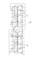
- FIG. 8 is a diagram showing the configuration of the amplifier circuit D5 according to the fifth embodiment.
- the amplifier circuit D5 according to the fifth embodiment uses a transistor for on / off control inserted in the source side of each transistor included in the first current mirror circuit CM1 and the second current mirror circuit CM2, and has a size parameter a. , B, and c are individually controlled, and the DC gain and boost gain are variably amplified.
- the amplifier circuit D5 is a differential amplifier that inputs input currents I IP and I IN and outputs output currents I OP and I ON.
- the amplifier circuit D5 has A first circuits 11 (hereinafter referred to as "group of first circuits”) connected in parallel.
- the amplifier circuit D5 has B second circuits 12 (hereinafter referred to as "group of second circuits") connected in parallel.
- the amplifier circuit D5 has C seventh circuits 17 (hereinafter referred to as "group of seventh circuits") connected in parallel.
- the amplifier circuit D5 has A + B + C third circuits 13 (hereinafter referred to as "group of third circuits") connected in parallel.
- the number of the third circuit 13 included in the group of the third circuit is the number of the first circuit 11 included in the group of the first circuit, the number of the second circuit 12 included in the group of the second circuit, and the first. It is equal to the total number of 7th circuits 17 included in the group of 7 circuits.
- the amplifier circuit D5 has A fourth circuits 14 (hereinafter referred to as "group of fourth circuits") connected in parallel.
- the amplifier circuit D5 has B fifth circuits 15 (hereinafter referred to as "group of fifth circuits”) connected in parallel.
- the amplifier circuit D5 has C eighth circuits 18 (hereinafter referred to as "group of eighth circuits") connected in parallel.
- the amplifier circuit D5 has A + B + C sixth circuits 16 (hereinafter referred to as "group of sixth circuits") connected in parallel.
- the number of the sixth circuit included in the group of the sixth circuit is the number of the fourth circuit 14 included in the group of the fourth circuit, the number of the fifth circuit 15 included in the group of the fifth circuit, and the eighth. Equal to the sum of the number of eighth circuits 18 contained in the group of circuits.
- the group of the first circuit, the group of the second circuit, and the group of the seventh circuit constitute the group of the third circuit and the group of the first current mirror circuit CM1. Further, the group of the fourth circuit, the group of the fifth circuit, and the group of the sixth circuit constitute the group of the eighth circuit and the group of the second current mirror circuit CM2. Further, the amplifier circuit D5 has a controller 25.
- Each first circuit 11 has a ninth transistor 112 connected in series with the first transistor 111.
- the ninth transistor 112 is, for example, an n-channel transistor, and the drain electrode of the ninth transistor 112 is connected to the source electrode of the first transistor 111.
- the source electrode of the ninth transistor 112 is connected to the reference potential node 31.
- the gate electrode of the ninth transistor 112 is connected to a predetermined fixed potential node, for example, a power potential node.
- the size parameter of the first transistor 111 is "1".
- the A first transistors 111 connected in parallel in the group of the first circuit form a part of the group of transistors that carry a current I a at a ratio corresponding to the size parameter a.
- each second circuit 12 includes a tenth transistor 122 for on / off control, an eleventh transistor 123, and a twelfth transistor 124 for on / off control. It has 1 inverter 128.
- the tenth transistor 122 is, for example, an n-channel transistor, and is connected between the second transistor 121 and the reference potential node 31.
- the drain electrode of the tenth transistor 122 is connected to the source electrode of the second transistor 121.
- the source electrode of the tenth transistor 122 is connected to the reference potential node 31.
- the gate electrode of the tenth transistor 122 is connected to the first control node 33.
- the size parameter of the second transistor 121 is "1".
- the B second transistors 121 connected in parallel in the second circuit group form part of a group of transistors that, when turned on, carry a current I b at a ratio corresponding to the size parameter b. Is.
- the eleventh transistor 123 is, for example, an n-channel transistor, and is connected in parallel with the first transistor 111 and the second transistor 121 between the input node 51 and the reference potential node 31.
- the drain electrode of the 11th transistor 123 is connected to the input node 51.
- the source electrode of the 11th transistor 123 is connected to the drain electrode of the 12th transistor 124.
- the gate electrode of the eleventh transistor 123 is connected to the gate electrode of the first transistor 111 without passing through the low-pass filter circuit 127.
- the size parameter of the 11th transistor 123 is "1".
- the B eleventh transistors 123 connected in parallel in the second circuit group form a part of a group of transistors that, when turned on, carry a current I a at a ratio corresponding to the size parameter a. Is.
- the twelfth transistor 124 is, for example, an n-channel transistor, and is connected between the eleventh transistor 123 and the reference potential node 31.
- the source electrode of the twelfth transistor 124 is connected to the reference potential node 31.
- the input side of the first inverter 128 is connected to the gate electrode of the tenth transistor 122, that is, the first control node 33.
- the output side of the first inverter 128 is connected to the gate electrode of the twelfth transistor 124.
- the first inverter 128 selectively turns on one of the tenth transistor 122 and the twelfth transistor 124 according to the input control signal.
- the controller 25 supplies a control signal (for example, a high level signal) for turning on the tenth transistor 122 and passing a current through the second transistor 121 to the first control node 33.
- a control signal for example, a high level signal
- the tenth transistor 122 is turned on by the high level signal, and a current I 1 having a ratio corresponding to the size parameter “1” flows through the second transistor 121.
- the high level signal is also supplied to the first inverter 128.
- the first inverter 128 supplies a low-level signal obtained by inverting the supplied high-level signal to the gate electrode of the twelfth transistor 124.
- the twelfth transistor 124 is not turned on because the control signal supplied to the gate electrode is a low level signal.
- the controller 25 supplies a control signal (for example, a low level signal) for turning off the tenth transistor 122 to the first control node 33.
- a control signal for example, a low level signal
- the 10th transistor 122 is turned off by the low level signal, and the current I 1 does not flow through the second transistor 121.
- the low level signal is also supplied to the first inverter 128.
- the first inverter 128 supplies a high-level signal obtained by inverting the supplied low-level signal to the gate electrode of the twelfth transistor 124.
- Twelfth transistor 124 is turned on because the control signal supplied to the gate electrode is at a high level signal, the size parameter "1" a current flows I 1 of the ratio corresponding to the eleventh transistor 123.
- Each 7th circuit 17 has a 7th transistor 171 and a 13th transistor 172, a 14th transistor 173, a 15th transistor 174, and a second inverter 175.
- the seventh transistor 171 is, for example, an n-channel transistor, and is connected in parallel with the fourth transistor 141 and the fifth transistor 151 between the input node 53 and the reference potential node 31.
- the drain electrode of the seventh transistor 171 is connected to the input node 53.
- the source electrode of the 7th transistor 171 is connected to the drain electrode of the 13th transistor 172.
- the gate electrode of the seventh transistor 171 is connected to the gate electrode of the first transistor 111.
- the size parameter of the 7th transistor 171 is "1".
- C-number of the seventh transistor 171 are connected in parallel, if it is turned on, constitutes a part of the group of transistors to flow a current -I c ratio corresponding to the size parameter c It is a thing.
- the 13th transistor 172 is, for example, an n-channel transistor, and is connected between the 7th transistor 171 and the reference potential node 31.
- the source electrode of the thirteenth transistor 172 is connected to the reference potential node 31.
- the 14th transistor 173 is, for example, an n-channel transistor, and is connected in parallel with the first transistor 111 and the second transistor 121 between the input node 51 and the reference potential node 31.
- the drain electrode of the 14th transistor 173 is connected to the input node 51.
- the source electrode of the 14th transistor 173 is connected to the drain electrode of the 15th transistor 174.
- the gate electrode of the 14th transistor 173 is connected to the gate electrode of the first transistor 111.
- the size parameter of the 14th transistor 173 is "1".
- the C 14th transistors 173 connected in parallel in the 7th circuit group constitute a part of the group of transistors that, when turned on, carry a current I a at a ratio corresponding to the size parameter a. Is.
- the 15th transistor 174 is, for example, an n-channel transistor, and is connected between the 14th transistor 173 and the reference potential node 31.
- the source electrode of the 15th transistor 174 is connected to the reference potential node 31.
- the gate electrode of the 15th transistor 174 is connected to the second control node 34.
- the input side of the second inverter 175 is connected to the gate electrode of the 15th transistor 174, that is, the second control node 34.
- the output side of the second inverter 175 is connected to the gate electrode of the thirteenth transistor 172.
- the second inverter 175 selectively turns on either the 13th transistor 172 or the 15th transistor 174 according to the input control signal.
- the controller 25 supplies a high-level signal for turning on the fifteenth transistor 174 and passing a current through the fourteenth transistor 173 to the second control node 34.
- the 15th transistor 174 is turned on by the high level signal, and a current I 1 having a ratio corresponding to the size parameter “1” flows through the 14th transistor 173.
- the high level signal is also supplied to the second inverter 175.
- the second inverter 175 supplies a low-level signal obtained by inverting the supplied high-level signal to the gate electrode of the thirteenth transistor 172.
- the thirteenth transistor 172 is not turned on because the control signal supplied to the gate electrode is a low level signal.
- the controller 25 supplies a low level signal for turning off the 14th transistor 173 to the second control node 34.
- the 15th transistor 174 is turned off by the low level signal, and the current I 1 does not flow through the 14th transistor 173.
- the low level signal is also supplied to the second inverter 175.
- the second inverter 175 supplies a high-level signal obtained by inverting the supplied low-level signal to the gate electrode of the thirteenth transistor 172. Thirteenth transistor 172 is turned on because the control signal supplied to the gate electrode is at a high level signal, the size parameter "1" a current flows -I 1 ratio corresponding to the seventh transistor 171.
- Each third circuit 13 has a 16th transistor 132 connected between the 3rd transistor 131 and the reference potential node 31.
- the 16th transistor 132 is, for example, an n-channel transistor, and the drain electrode of the 16th transistor 132 is connected to the source electrode of the 3rd transistor 131.
- the source electrode of the 16th transistor 132 is connected to the reference potential node 31.
- the gate electrode of the 16th transistor 132 is connected to a predetermined fixed potential node, for example, a power potential node.
- the size parameter of the third transistor 131 is "1".
- the A + B + C third transistors 131 connected in parallel in the third circuit group constitute a group of transistors that carry a current I a + b + c at a ratio corresponding to the size parameter a + b + c.
- the first transistor 111, the second transistor 121, the third transistor 131, the seventh transistor 171 and the eleventh transistor 123, and the 14th transistor 173 have the sizes thereof.
- the parameters are all "1" and the sizes are equal to each other.
- Each fourth circuit 14 has a 17th transistor 142 connected between the 4th transistor 141 and the reference potential node 31.
- the 17th transistor 142 is, for example, an n-channel transistor, and the drain electrode of the 17th transistor 142 is connected to the source electrode of the 4th transistor 141.
- the source electrode of the 17th transistor 142 is connected to the reference potential node 31.
- the gate electrode of the 17th transistor 142 is connected to a predetermined fixed potential node, for example, a power potential node.
- the size parameter of the fourth transistor 141 is "1".
- the A fourth transistor 141 connected in parallel in the fourth circuit group constitutes a part of the group of transistors that carry a current ⁇ Ia at a ratio corresponding to the size parameter a.
- Each fifth circuit 15 has an 18th transistor 152, a 19th transistor 153, a 20th transistor 154, and a third inverter 158 in addition to the 5th transistor 151 and the low-pass filter circuit 157.
- the 18th transistor 152 is, for example, an n-channel transistor, and is connected between the 5th transistor 151 and the reference potential node 31.
- the drain electrode of the 18th transistor 152 is connected to the source electrode of the 5th transistor 151.
- the source electrode of the 18th transistor 152 is connected to the reference potential node 31.
- the gate electrode of the 18th transistor 152 is connected to the third control node 35.
- the size parameter of the fifth transistor 151 is "1".
- the B fifth transistors 151 connected in parallel in the fifth circuit group form part of a group of transistors that, when turned on, carry a current ⁇ I b at a ratio corresponding to the size parameter b. It is a thing.
- the 19th transistor 153 is, for example, an n-channel transistor, and is connected in parallel with the 4th transistor 141 and the 5th transistor 151 between the input node 53 and the reference potential node 31.
- the drain electrode of the 19th transistor 153 is connected to the input node 53.
- the source electrode of the 19th transistor 153 is connected to the drain electrode of the 20th transistor 154.
- the gate electrode of the 19th transistor 153 is connected to the gate electrode of the 4th transistor 141 without passing through the low-pass filter circuit 157.
- the size parameter of the 19th transistor 153 is "1".
- the B 19th transistors 153 connected in parallel in the fifth circuit group form part of a group of transistors that, when turned on, carry a current ⁇ Ia at a ratio corresponding to the size parameter a. It is a thing.
- the 20th transistor 154 is, for example, an n-channel transistor, and is connected between the 19th transistor 153 and the reference potential node 31.
- the source electrode of the 20th transistor 154 is connected to the reference potential node 31.
- the input side of the third inverter 158 is connected to the gate electrode of the 18th transistor 152, that is, the third control node 35.
- the output side of the third inverter 158 is connected to the gate electrode of the 20th transistor 154.
- the third inverter 158 selectively turns on either the 18th transistor 152 or the 20th transistor 154 according to the input control signal.
- Each 8th circuit 18 has an 8th transistor 181 and a 21st transistor 182, a 22nd transistor 183, a 23rd transistor 184, and a 4th inverter 185.
- the eighth transistor 181 is, for example, an n-channel transistor, and is connected in parallel with the first transistor 111 and the second transistor 121 between the input node 51 and the reference potential node 31.
- the drain electrode of the eighth transistor 181 is connected to the input node 51.
- the source electrode of the eighth transistor 181 is connected to the drain electrode of the 21st transistor 182.
- the gate electrode of the eighth transistor 181 is connected to the gate electrode of the fourth transistor 141.
- the size parameter of the eighth transistor 181 is "1".
- C-number of the eighth transistor 181 are connected in parallel, if it is turned on, constitutes a part of the group of transistors to flow a current I c of the ratio corresponding to the size parameter c Is.
- the 21st transistor 182 is, for example, an n-channel transistor, and is connected between the 8th transistor 181 and the reference potential node 31.
- the source electrode of the 21st transistor 182 is connected to the reference potential node 31.
- the 22nd transistor 183 is, for example, an n-channel transistor, and is connected in parallel with the 4th transistor 141 and the 5th transistor 151 between the input node 53 and the reference potential node 31.
- the drain electrode of the 22nd transistor 183 is connected to the input node 53.
- the source electrode of the 22nd transistor 183 is connected to the drain electrode of the 23rd transistor 184.
- the gate electrode of the 22nd transistor 183 is connected to the gate electrode of the 4th transistor 141.
- the size parameter of the 22nd transistor 183 is "1".
- the size parameter of the 22nd transistor 183 is "1".
- the C 22nd transistors 183 connected in parallel in the group of eighth circuits form part of a group of transistors that, when turned on, carry a current ⁇ I a at a ratio corresponding to the size parameter a. It is a thing.
- the 23rd transistor 184 is, for example, an n-channel transistor, and is connected between the 22nd transistor 183 and the reference potential node 31.
- the source electrode of the 23rd transistor 184 is connected to the reference potential node 31.
- the gate electrode of the 23rd transistor 184 is connected to the 4th control node 36.
- the input side of the 4th inverter 185 is connected to the gate electrode of the 23rd transistor 184, that is, the 4th control node 36.
- the output side of the fourth inverter 185 is connected to the gate electrode of the 21st transistor 182.
- the fourth inverter 185 selectively turns on either the 21st transistor 182 or the 23rd transistor 184 according to the input control signal.
- Each sixth circuit 16 has a 24th transistor 162 connected between the 6th transistor 161 and the reference potential node 31.
- the 24th transistor 162 is, for example, an n-channel transistor, and the drain electrode of the 24th transistor 162 is connected to the source electrode of the 6th transistor 161.
- the source electrode of the 24th transistor 162 is connected to the reference potential node 31.
- the gate electrode of the 24th transistor 162 is connected to a predetermined fixed potential node, for example, a power potential node.
- the size parameter of the sixth transistor 161 is "1".
- the A + B + C sixth transistors 161 connected in parallel in the sixth circuit group constitute a part of the group of transistors that carry a current ⁇ I a + b + c at a ratio corresponding to the size parameter a + b + c.
- the fourth transistor 141, the fifth transistor 151, the sixth transistor 161 and the eighth transistor 181, the 19th transistor 153, and the 22nd transistor 183 have size parameters thereof. Are all "1" and the sizes are equal to each other.
- the controller 25 selectively inputs a plurality of first control signals to the group of the second circuit and selectively inputs the plurality of second control signals to the group of the seventh circuit according to the set DC gain and boost gain.
- This is a control circuit that variably performs input, selective input of a plurality of third control signals to a group of fifth circuits, and selective input of a plurality of fourth control signals to a group of eighth circuits.
- the difference in gain between the case where the frequency ⁇ of the input currents I IP and I IN is larger and smaller than the cutoff frequency ⁇ z of the low-pass filter circuit 127 and the low-pass filter circuit 157 is the first. It is determined according to the number of second transistors 121 turned on by one control signal and the number of fifth transistors 151 turned on by a third control signal.
- the gain when the frequency ⁇ of the input currents I IP and I IN is smaller than the cutoff frequency ⁇ z of the low-pass filter circuit 127 and the low-pass filter circuit 157 is turned on by the second control signal. It is determined according to the number of 7 transistors 171 and the number of 8th transistors 181 turned on by the 4th control signal.
- the amplifier circuit D5 is input current I IP, the gain when the frequency of the I IN omega is greater than the cut-off frequency omega z of the low-pass filter circuit 127 and the low-pass filter circuit 157, the input current I IP, the I IN It is larger than the gain when the frequency ⁇ is smaller than the cutoff frequency ⁇ z of the low-pass filter circuit 127 and the low-pass filter circuit 157.
- the controller 25 has a plurality of first control nodes 33, a plurality of second control nodes 34, a plurality of third control nodes 35, and a plurality of third control nodes, depending on the DC gain and boost gain to be set.
- a corresponding control signal is supplied to the fourth control node 36.
- the controller 25 stores a look-up table for determining the size parameters a, b, c based on the set DC gain and boost gain.
- the controller 25 determines the values of the size parameters a, b, and c based on the set DC gain and boost gain and the look-up table.
- the controller 25 outputs the corresponding control signals for setting the determined values of the size parameters a, b, and c to the plurality of first control nodes 33, the plurality of second control nodes 34, and the plurality of third control nodes 35. And supply to the fourth control node 36.
- This switching control is performed using the size parameters a, b, c determined based on the level of DC gain and the level of boost gain.
- the size parameters a, b, and c use DC gain and boost gain as input information, and the respective values of the size parameters a, b, and c (that is, in the first current mirror circuit CM1, the current of the ratio corresponding to each size parameter is used.
- the number of transistors to be driven to flow) is used as output information and is determined using a lookup table.
- FIGS. 9A, 9B, and 9C are look-up tables for determining the size parameters a, b, and c based on the set DC gain and boost gain.
- EQ means the level of boost gain
- VGA means the level of DC gain.
- a control signal for example, a high level signal
- a control signal for example, a low level signal for turning on the 12th transistor 124 and passing a current through the 11th transistor 123 is supplied to the first control node 33.
- a control signal for example, a low level signal
- a control signal for example, a low level signal
- a control signal for example, a high level signal for turning on the 15th transistor 174 and passing a current through the 14th transistor 173 is not supplied.
- the second transistor 121 whose size parameter is “1" is turned on for the three second circuits 12 out of the 14 second circuits 12, and the remaining 11 second circuits 12 are controlled.
- the circuit 12 is controlled to turn on the eleventh transistor 123 whose size parameter is “1”.
- the 7th transistor 171 whose size parameter is "1" is turned on for the 10 7th circuits 17 out of the 10 7th circuits 17, and the 10th 7th circuits 17 are controlled.
- the 14th transistor 173 whose size parameter is "1" is controlled so that none of them is turned on.
- the size parameters a, b, and c may be determined at any time. For example, it can be performed at the time of starting the device on which the amplifier circuit D5 is mounted.
- the amplifier circuit D5 by setting the desired DC gain and boost gain (peak gain), the size parameter a for realizing the setting by the look-up table. , B, c can be determined automatically.
- the amplifier circuit D5 can execute switching control according to the determined size parameters a, b, and c to amplify the DC gain and the boost gain.
- the user can set the DC gain and the boost gain individually and variably. This makes it possible to further cope with the increase in the signal amplitude level.
- the amplifier circuit D6 according to the sixth embodiment is for connecting any one of the amplifier circuits D1 to D5 in multiple stages to realize a larger DC gain and boost gain.
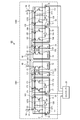
- FIG. 10 is a diagram showing the configuration of the amplifier circuit D6 according to the sixth embodiment, and illustrates a case where the amplifier circuit D3 is connected in two stages.
- the output node of the amplifier circuit D3 configured by the n-channel transistor is connected to the input node of the amplifier circuit D3'configured by replacing the n-channel transistor of the amplifier circuit D3 with the p-channel transistor. Two-stage connection is realized.
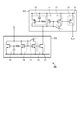
- FIG. 11 is a diagram showing the configuration of the receiving circuit D7 according to the seventh embodiment.
- the receiving circuit D7 includes a CTLE 81, a DFE (Decision feedback equalizer) 82, and a DEMUX (Demultiplexer) 83.
- CTLE 81 CTLE
- DFE Decision feedback equalizer
- DEMUX Demultiplexer
- the CTLE 81 has each amplifier circuit according to the first to sixth embodiments inside, and is continuously on the time axis with respect to the differential input signal (serial input signal) received by the differential input terminals 84 and 85. It is an input amplification circuit that performs amplification processing and equalization processing.
- the DFE 82 is an equalization circuit that receives the output signal of the CTLE 81 and performs equalization processing by a feedback loop and determination of the signal level for the output signal of the CTLE 81. Note that CTLE81 and DFE82 are examples of input circuits.
- the DEMUX83 is a conversion circuit that receives the output signal of the DFE82 and performs a conversion process of converting the output signal of the DFE82 from serial to parallel.
- FIG. 12 is a diagram showing the configuration of the semiconductor integrated circuit D8 according to the eighth embodiment. As shown in FIG. 12, the semiconductor integrated circuit D8 has a processing circuit 7 that executes predetermined signal processing on the output signals of the receiving circuit 80 and the receiving circuit 80.
- the receiving circuit 80 is, for example, the receiving circuit D7 shown in FIG. 11, and the CTLE 81 in the receiving circuit 80 has each amplifier circuit according to the first to sixth embodiments inside.
- a first circuit including a first transistor connected between an input node through which an input current flows and a reference potential node and a gate electrode connected to the input node.
- a second unit that includes a low-pass filter circuit, is connected in parallel with the first transistor between the input node and the reference potential node, and the gate electrode is connected to the gate electrode of the first transistor via the low-pass filter circuit.
- the second circuit including the transistor and A third circuit including a third transistor connected between the output node through which the output current flows and the reference potential node and the gate electrode connected to the gate electrode of the first transistor.
- Appendix 2 The amplifier circuit according to Appendix 1, wherein the first circuit and the second circuit constitute the third circuit and a current mirror circuit.
- the low-pass filter circuit is A capacitor connected between the gate electrode of the second transistor and the reference potential node,
- the amplifier circuit according to Appendix 1 or 2 which includes a resistor connected between the gate electrode of the second transistor and the gate electrode of the first transistor.
- Appendix 5 The amplifier circuit according to Appendix 4, wherein the first transistor, the second transistor, and the third transistor are planar transistors, respectively, and the size corresponds to the gate width of the planar transistor.
- Appendix 8 The amplifier circuit according to Appendix 7, wherein the gain of the amplifier circuit when the frequency of the input current is smaller than the cutoff frequency of the low-pass filter circuit is determined according to the size of the current source.
- Appendix 10 The amplification according to Appendix 9, wherein the difference in gain of the amplifier circuit between the case where the frequency of the input current is larger than the cutoff frequency of the low-pass filter circuit and the case where the frequency is smaller than the cutoff frequency of the low-pass filter circuit is determined according to the size of the second transistor. circuit.
- a first circuit including a first transistor connected between a first input node through which a first input current flows and a reference potential node and a gate electrode connected to the first input node.
- a first low-pass filter circuit is included, connected in parallel with the first transistor between the first input node and the reference potential node, and a gate electrode is interposed via the gate electrode of the first transistor and the first low-pass filter circuit.
- the second circuit including the second transistor connected by A third circuit including a third transistor connected between the first output node through which the first output current flows and the reference potential node and the gate electrode connected to the gate electrode of the first transistor.
- a fourth circuit including a fourth transistor connected between the second input node through which the second input current flows and the reference potential node and the gate electrode connected to the second input node.
- a second low-pass filter circuit is included, connected in parallel with the fourth transistor between the second input node and the reference potential node, and a gate electrode is interposed via the gate electrode of the fourth transistor and the second low-pass filter circuit.
- the fifth circuit including the fifth transistor connected by A sixth circuit including a sixth transistor connected between the second output node through which the second output current flows and the reference potential node and the gate electrode connected to the gate electrode of the fourth transistor.
- a seventh circuit including a seventh transistor connected between the second input node and the reference potential node and having a gate electrode connected to the gate electrode of the first transistor.
- An eighth circuit including an eighth transistor connected between the first input node and the reference potential node and having a gate electrode connected to the gate electrode of the fourth transistor.
- the first circuit, the second circuit, and the seventh circuit constitute the third circuit and the first current mirror circuit.
- the differential amplifier circuit according to Appendix 11 wherein the fourth circuit, the fifth circuit, and the eighth circuit constitute the sixth circuit and the second current mirror circuit.
- the first low-pass filter circuit is A first capacitor connected between the gate electrode of the second transistor and the reference potential node, It includes a first resistor connected between the gate electrode of the second transistor and the gate electrode of the first transistor.
- the second low-pass filter circuit is A second capacitor connected between the gate electrode of the fifth transistor and the reference potential node,
- the size of the third transistor is equal to the sum of the size of the first transistor, the size of the second transistor, and the size of the seventh transistor.
- the second circuit is connected in parallel with the tenth transistor connected between the second transistor and the reference potential node, and the second transistor between the first input node and the reference potential node, and is gated.
- the eleventh transistor whose electrodes are connected to the gate of the first transistor without passing through the first low-pass filter circuit, the twelfth transistor connected between the eleventh transistor and the reference potential node, and the tenth transistor.
- One of the input side and the output side is connected to the gate electrode of the transistor, the other of the input side and the output side is connected to the gate electrode of the twelfth transistor, and the tenth is corresponding to the input first control signal.
- the seventh circuit has a transistor and a first inverter that selectively transitions one of the twelfth transistors to ON.
- the seventh circuit is connected in parallel with the thirteenth transistor connected between the seventh transistor and the reference potential node, and the seventh transistor between the first input node and the reference potential node, and is gated.
- the 14th transistor whose electrodes are connected to the gate of the 1st transistor, the 15th transistor connected between the 14th transistor and the reference potential node, and the input side and output side to the gate electrode of the 15th transistor.
- One of the 13th transistor and the other of the output side are connected to the gate electrode of the 13th transistor, and either the 13th transistor or the 15th transistor is connected according to the input second control signal.
- the fifth circuit is connected in parallel with the eighteenth transistor connected between the fifth transistor and the reference potential node, and the fifth transistor between the second input node and the reference potential node, and is gated.
- the 19th transistor whose electrodes are connected to the gate of the 4th transistor without passing through the 2nd low-pass filter circuit, the 20th transistor connected between the 19th transistor and the reference potential node, and the 18th transistor.
- One of the input side and the output side is connected to the gate electrode of the transistor, and the other side of the input side and the output side is connected to the gate electrode of the 20th transistor. It has a transistor and a third inverter that selectively transitions either one of the 20th transistors to ON.
- the eighth circuit is connected in parallel with the 21st transistor connected between the 8th transistor and the reference potential node, and in parallel with the 8th transistor between the 2nd input node and the reference potential node, and is a gate.
- the 22nd transistor whose electrode is connected to the gate of the 4th transistor, the 23rd transistor connected between the 22nd transistor and the reference potential node, and one of the input sides to the gate electrode of the 23rd transistor
- the other of the input side and the output side is connected to the gate electrode of the 21st transistor, and either the 21st transistor or the 23rd transistor is selectively selected according to the input 4th control signal.
- the group of 7 circuits constitutes the group of the 3rd circuit including the 3rd circuit connected in parallel and the 1st current mirror circuit.
- the group of circuits constitutes the group of the sixth circuit including the sixth circuit connected in parallel and the second current mirror circuit.
- a control circuit that variably performs a plurality of selective inputs of the third control signal to the group of the fifth circuit and a plurality of selective inputs of the fourth control signal to the group of the eighth circuit.
- the differential amplifier circuit according to Appendix 15, including the above.
- the DC gain is the gain of the amplifier circuit when the frequency of the input current is smaller than the cutoff frequency of the low-pass filter circuit.
- the differential amplifier circuit according to Appendix 16 wherein the boost gain is a gain of the amplifier circuit when the frequency of the input current is larger than the cutoff frequency of the low-pass filter circuit.
- the number of the third circuit included in the group of the third circuit is the number of the first circuit included in the group of the first circuit, the number of the second circuit included in the group of the second circuit, and the number of the second circuit. Equal to the total number of 7th circuits included in the 7th circuit group, The number of the sixth circuit included in the group of the sixth circuit is the number of the fourth circuit included in the group of the fourth circuit, the number of the fifth circuit included in the group of the fifth circuit, and the number of the fifth circuit.
- the differential amplifier circuit according to Appendix 16 or 17, which is equal to the total number of the eighth circuits included in the group of the eighth circuits.
- Appendix 24 The difference described in Appendix 23, wherein the gain of the amplifier circuit when the frequency of the input current is smaller than the cutoff frequency of the low-pass filter circuit is determined according to the sizes of the first current source and the second current source. Dynamic amplifier circuit.
- Appendix 28 The receiving circuit described in Appendix 27 and A semiconductor integrated circuit having a processing circuit that executes predetermined signal processing with respect to the output signal of the receiving circuit.
- the amplifier circuit, the differential amplifier circuit, the receiver circuit, and the semiconductor integrated circuit according to the embodiment disclosed in the present specification have a boost gain amplification function and a small area while maintaining the linearity of the gain. Realize.
Landscapes
- Engineering & Computer Science (AREA)
- Power Engineering (AREA)
- Microelectronics & Electronic Packaging (AREA)
- Physics & Mathematics (AREA)
- Nonlinear Science (AREA)
- Electromagnetism (AREA)
- General Physics & Mathematics (AREA)
- Radar, Positioning & Navigation (AREA)
- Automation & Control Theory (AREA)
- Amplifiers (AREA)
Priority Applications (4)
| Application Number | Priority Date | Filing Date | Title |
|---|---|---|---|
| JP2022529974A JP7567909B2 (ja) | 2020-06-11 | 2020-06-11 | 増幅回路、差動増幅回路、受信回路及び半導体集積回路 |
| PCT/JP2020/023110 WO2021250870A1 (ja) | 2020-06-11 | 2020-06-11 | 増幅回路、差動増幅回路、受信回路及び半導体集積回路 |
| CN202080101881.XA CN115699568B (zh) | 2020-06-11 | 2020-06-11 | 放大电路、差动放大电路、接收电路以及半导体集成电路 |
| US18/061,757 US20230095506A1 (en) | 2020-06-11 | 2022-12-05 | Amplifier circuit, differential amplifier circuit, reception circuit, and semiconductor integrated circuit |
Applications Claiming Priority (1)
| Application Number | Priority Date | Filing Date | Title |
|---|---|---|---|
| PCT/JP2020/023110 WO2021250870A1 (ja) | 2020-06-11 | 2020-06-11 | 増幅回路、差動増幅回路、受信回路及び半導体集積回路 |
Related Child Applications (1)
| Application Number | Title | Priority Date | Filing Date |
|---|---|---|---|
| US18/061,757 Continuation US20230095506A1 (en) | 2020-06-11 | 2022-12-05 | Amplifier circuit, differential amplifier circuit, reception circuit, and semiconductor integrated circuit |
Publications (1)
| Publication Number | Publication Date |
|---|---|
| WO2021250870A1 true WO2021250870A1 (ja) | 2021-12-16 |
Family
ID=78847077
Family Applications (1)
| Application Number | Title | Priority Date | Filing Date |
|---|---|---|---|
| PCT/JP2020/023110 Ceased WO2021250870A1 (ja) | 2020-06-11 | 2020-06-11 | 増幅回路、差動増幅回路、受信回路及び半導体集積回路 |
Country Status (4)
| Country | Link |
|---|---|
| US (1) | US20230095506A1 (https=) |
| JP (1) | JP7567909B2 (https=) |
| CN (1) | CN115699568B (https=) |
| WO (1) | WO2021250870A1 (https=) |
Citations (3)
| Publication number | Priority date | Publication date | Assignee | Title |
|---|---|---|---|---|
| US6545540B1 (en) * | 2000-10-11 | 2003-04-08 | Intersil Americas Inc. | Current mirror-embedded low-pass filter for subscriber line interface circuit applications |
| JP2005526412A (ja) * | 2001-07-30 | 2005-09-02 | フリースケール セミコンダクター インコーポレイテッド | 能動バイアス回路 |
| JP2009165100A (ja) * | 2007-12-11 | 2009-07-23 | Hitachi Metals Ltd | 高周波増幅器及び高周波モジュール並びにそれらを用いた移動体無線機 |
Family Cites Families (8)
| Publication number | Priority date | Publication date | Assignee | Title |
|---|---|---|---|---|
| FR2688905A1 (fr) * | 1992-03-18 | 1993-09-24 | Philips Composants | Circuit miroir de courant a commutation acceleree. |
| JPH0974340A (ja) * | 1995-09-04 | 1997-03-18 | Toshiba Corp | コンパレータ回路 |
| EP1806639A1 (en) * | 2006-01-10 | 2007-07-11 | AMI Semiconductor Belgium BVBA | A DC current regulator insensitive to conducted EMI |
| TWI323556B (en) * | 2006-07-28 | 2010-04-11 | Realtek Semiconductor Corp | Hybrid output stage circuit and related method thereof |
| JP5120248B2 (ja) * | 2008-12-26 | 2013-01-16 | 富士通株式会社 | 増幅回路 |
| KR101099699B1 (ko) * | 2010-04-02 | 2011-12-28 | 부산대학교 산학협력단 | 고선형성, 저전력에 적합한 가변이득 증폭기 및 이를 이용한 rf송신기 |
| JP7181470B2 (ja) * | 2018-02-08 | 2022-12-01 | 株式会社ソシオネクスト | 加算回路、受信回路及び集積回路 |
| CN114788174B (zh) * | 2019-12-17 | 2025-04-22 | 株式会社索思未来 | 差动放大电路、接收电路以及半导体集成电路 |
-
2020
- 2020-06-11 JP JP2022529974A patent/JP7567909B2/ja active Active
- 2020-06-11 CN CN202080101881.XA patent/CN115699568B/zh active Active
- 2020-06-11 WO PCT/JP2020/023110 patent/WO2021250870A1/ja not_active Ceased
-
2022
- 2022-12-05 US US18/061,757 patent/US20230095506A1/en active Pending
Patent Citations (3)
| Publication number | Priority date | Publication date | Assignee | Title |
|---|---|---|---|---|
| US6545540B1 (en) * | 2000-10-11 | 2003-04-08 | Intersil Americas Inc. | Current mirror-embedded low-pass filter for subscriber line interface circuit applications |
| JP2005526412A (ja) * | 2001-07-30 | 2005-09-02 | フリースケール セミコンダクター インコーポレイテッド | 能動バイアス回路 |
| JP2009165100A (ja) * | 2007-12-11 | 2009-07-23 | Hitachi Metals Ltd | 高周波増幅器及び高周波モジュール並びにそれらを用いた移動体無線機 |
Also Published As
| Publication number | Publication date |
|---|---|
| CN115699568B (zh) | 2025-11-18 |
| JPWO2021250870A1 (https=) | 2021-12-16 |
| JP7567909B2 (ja) | 2024-10-16 |
| US20230095506A1 (en) | 2023-03-30 |
| CN115699568A (zh) | 2023-02-03 |
Similar Documents
| Publication | Publication Date | Title |
|---|---|---|
| US8558611B2 (en) | Peaking amplifier with capacitively-coupled parallel input stages | |
| JP3318725B2 (ja) | アナログフィルタ回路 | |
| CN103329429B (zh) | 用于多级放大器的米勒补偿的装置和方法 | |
| US6985036B2 (en) | Digitally controlled transconductance cell | |
| TW201012050A (en) | Three-stage frequency-compensated operational amplifier | |
| US20030169104A1 (en) | Miller de-compensation for differential input, differential output amplifier | |
| US20120038419A1 (en) | Mitigating side effects of impedance transformation circuits | |
| KR19980064159A (ko) | 필터 회로 | |
| US5321370A (en) | Operational amplifier with common-mode feedback amplifier circuit | |
| US6977541B2 (en) | Variable time constant circuit and filter circuit using the same | |
| CN110649900A (zh) | 一种高信噪比两级运算放大器 | |
| CN107171650B (zh) | 可变增益放大电路 | |
| WO2004077666A1 (ja) | 利得可変電圧・電流変換回路とこれを用いたフィルタ回路 | |
| CN210351102U (zh) | 一种麦克风可编程增益放大器集成电路 | |
| WO2021250870A1 (ja) | 増幅回路、差動増幅回路、受信回路及び半導体集積回路 | |
| CN216016845U (zh) | 一种缓冲器电路和一种电子设备 | |
| US7358813B2 (en) | Differential operational amplifier | |
| CN113489465B (zh) | 一种放大器电路 | |
| CN108781062B (zh) | 可变增益放大器 | |
| JP3930461B2 (ja) | 増幅回路及びこれを用いた液晶ディスプレイ装置 | |
| JP4572481B2 (ja) | トランスコンダクタ回路 | |
| JP3874649B2 (ja) | 平衡回路 | |
| JP2001339275A (ja) | フィルタ回路とこれを用いた検波回路 | |
| TWI787754B (zh) | 利用穿隧電流進行放大器偏壓控制 | |
| CN119363097A (zh) | 单端至差分信号转换电路及方法 |
Legal Events
| Date | Code | Title | Description |
|---|---|---|---|
| 121 | Ep: the epo has been informed by wipo that ep was designated in this application |
Ref document number: 20940020 Country of ref document: EP Kind code of ref document: A1 |
|
| WWE | Wipo information: entry into national phase |
Ref document number: 202080101881.X Country of ref document: CN |
|
| ENP | Entry into the national phase |
Ref document number: 2022529974 Country of ref document: JP Kind code of ref document: A |
|
| NENP | Non-entry into the national phase |
Ref country code: DE |
|
| 122 | Ep: pct application non-entry in european phase |
Ref document number: 20940020 Country of ref document: EP Kind code of ref document: A1 |