WO2021250870A1 - Amplification circuit, differential amplification circuit, reception circuit, and semiconductor integrated circuit - Google Patents
Amplification circuit, differential amplification circuit, reception circuit, and semiconductor integrated circuit Download PDFInfo
- Publication number
- WO2021250870A1 WO2021250870A1 PCT/JP2020/023110 JP2020023110W WO2021250870A1 WO 2021250870 A1 WO2021250870 A1 WO 2021250870A1 JP 2020023110 W JP2020023110 W JP 2020023110W WO 2021250870 A1 WO2021250870 A1 WO 2021250870A1
- Authority
- WO
- WIPO (PCT)
- Prior art keywords
- transistor
- circuit
- input
- node
- gate electrode
- Prior art date
Links
- 230000003321 amplification Effects 0.000 title claims abstract description 18
- 238000003199 nucleic acid amplification method Methods 0.000 title claims abstract description 18
- 239000004065 semiconductor Substances 0.000 title claims description 12
- 230000007704 transition Effects 0.000 claims description 8
- 238000006243 chemical reaction Methods 0.000 claims description 6
- 238000000034 method Methods 0.000 claims description 5
- 230000008569 process Effects 0.000 claims description 5
- 238000010586 diagram Methods 0.000 description 22
- 239000003990 capacitor Substances 0.000 description 9
- 230000007850 degeneration Effects 0.000 description 4
- 230000008859 change Effects 0.000 description 3
- 230000000694 effects Effects 0.000 description 2
- 238000001914 filtration Methods 0.000 description 2
- 230000004048 modification Effects 0.000 description 2
- 238000012986 modification Methods 0.000 description 2
- 230000004044 response Effects 0.000 description 2
- 230000005540 biological transmission Effects 0.000 description 1
- 239000002775 capsule Substances 0.000 description 1
- 238000005516 engineering process Methods 0.000 description 1
- 230000005669 field effect Effects 0.000 description 1
- 230000003071 parasitic effect Effects 0.000 description 1
- 230000009467 reduction Effects 0.000 description 1
Images


Classifications
-
- H—ELECTRICITY
- H03—ELECTRONIC CIRCUITRY
- H03F—AMPLIFIERS
- H03F3/00—Amplifiers with only discharge tubes or only semiconductor devices as amplifying elements
- H03F3/45—Differential amplifiers
- H03F3/45071—Differential amplifiers with semiconductor devices only
- H03F3/45076—Differential amplifiers with semiconductor devices only characterised by the way of implementation of the active amplifying circuit in the differential amplifier
- H03F3/45179—Differential amplifiers with semiconductor devices only characterised by the way of implementation of the active amplifying circuit in the differential amplifier using MOSFET transistors as the active amplifying circuit
- H03F3/45273—Mirror types
-
- G—PHYSICS
- G05—CONTROLLING; REGULATING
- G05F—SYSTEMS FOR REGULATING ELECTRIC OR MAGNETIC VARIABLES
- G05F3/00—Non-retroactive systems for regulating electric variables by using an uncontrolled element, or an uncontrolled combination of elements, such element or such combination having self-regulating properties
- G05F3/02—Regulating voltage or current
- G05F3/08—Regulating voltage or current wherein the variable is dc
- G05F3/10—Regulating voltage or current wherein the variable is dc using uncontrolled devices with non-linear characteristics
- G05F3/16—Regulating voltage or current wherein the variable is dc using uncontrolled devices with non-linear characteristics being semiconductor devices
- G05F3/20—Regulating voltage or current wherein the variable is dc using uncontrolled devices with non-linear characteristics being semiconductor devices using diode- transistor combinations
- G05F3/26—Current mirrors
- G05F3/262—Current mirrors using field-effect transistors only
-
- H—ELECTRICITY
- H03—ELECTRONIC CIRCUITRY
- H03F—AMPLIFIERS
- H03F1/00—Details of amplifiers with only discharge tubes, only semiconductor devices or only unspecified devices as amplifying elements
- H03F1/08—Modifications of amplifiers to reduce detrimental influences of internal impedances of amplifying elements
- H03F1/083—Modifications of amplifiers to reduce detrimental influences of internal impedances of amplifying elements in transistor amplifiers
- H03F1/086—Modifications of amplifiers to reduce detrimental influences of internal impedances of amplifying elements in transistor amplifiers with FET's
-
- H—ELECTRICITY
- H03—ELECTRONIC CIRCUITRY
- H03F—AMPLIFIERS
- H03F3/00—Amplifiers with only discharge tubes or only semiconductor devices as amplifying elements
- H03F3/34—DC amplifiers in which all stages are DC-coupled
- H03F3/343—DC amplifiers in which all stages are DC-coupled with semiconductor devices only
- H03F3/347—DC amplifiers in which all stages are DC-coupled with semiconductor devices only in integrated circuits
-
- H—ELECTRICITY
- H03—ELECTRONIC CIRCUITRY
- H03F—AMPLIFIERS
- H03F3/00—Amplifiers with only discharge tubes or only semiconductor devices as amplifying elements
- H03F3/45—Differential amplifiers
- H03F3/45071—Differential amplifiers with semiconductor devices only
- H03F3/45076—Differential amplifiers with semiconductor devices only characterised by the way of implementation of the active amplifying circuit in the differential amplifier
- H03F3/45179—Differential amplifiers with semiconductor devices only characterised by the way of implementation of the active amplifying circuit in the differential amplifier using MOSFET transistors as the active amplifying circuit
- H03F3/45183—Long tailed pairs
-
- H—ELECTRICITY
- H03—ELECTRONIC CIRCUITRY
- H03F—AMPLIFIERS
- H03F3/00—Amplifiers with only discharge tubes or only semiconductor devices as amplifying elements
- H03F3/45—Differential amplifiers
- H03F3/45071—Differential amplifiers with semiconductor devices only
- H03F3/45076—Differential amplifiers with semiconductor devices only characterised by the way of implementation of the active amplifying circuit in the differential amplifier
- H03F3/45475—Differential amplifiers with semiconductor devices only characterised by the way of implementation of the active amplifying circuit in the differential amplifier using IC blocks as the active amplifying circuit
-
- H—ELECTRICITY
- H03—ELECTRONIC CIRCUITRY
- H03F—AMPLIFIERS
- H03F2200/00—Indexing scheme relating to amplifiers
- H03F2200/474—A current mirror being used as sensor
Definitions
- One embodiment disclosed in the present specification and the like relates to, for example, an amplifier circuit, a differential amplifier circuit, a receiver circuit, and a semiconductor integrated circuit used in a CTLE (Continuous Time Liner Equalizer, continuous time linear equalizer).
- CTLE Continuous Time Liner Equalizer, continuous time linear equalizer
- CTLE is an input amplifier circuit of a SerDes (SERializer DESerializer) receiving circuit used for a high-speed interface for a network or a data center, and is used as a loss compensation circuit in a transmission line.
- the conventional CTLE uses a source degeneration type equalizer.
- the conventional CTLE using the source degeneration type equalizer realizes the boost gain amplification function by using the inductor element (coil). Therefore, the circuit size (area) becomes large. In addition, the gain becomes non-linear due to variation factors such as resistance and mutual conductance in the circuit.
- One of the problems to be solved by the embodiments disclosed in the present specification and the like is an amplifier circuit, a differential amplifier circuit, and a receiving circuit that realize a boost gain amplification function and a small area while maintaining the linearity of the gain. And to provide semiconductor integrated circuits.
- the amplifier circuit includes a first circuit including a first transistor connected between an input node through which an input current flows and a reference potential node, and a gate electrode connected to the input node, and a low-pass filter circuit.
- a second circuit including a second transistor connected in parallel with the first transistor between the input node and the reference potential node and having a gate electrode connected to the gate of the first transistor via the low pass filter circuit. It has a third circuit including a third transistor connected between the output node through which the output current flows and the reference potential node and the gate electrode connected to the gate of the first transistor.
- an amplifier circuit, a differential amplifier circuit, a receiver circuit, and a semiconductor integrated circuit that realize a boost gain amplification function and a small area while maintaining gain linearity are realized. be able to.
- FIG. 1 is a diagram showing a configuration of an amplifier circuit according to the first embodiment.
- FIG. 2 is a diagram showing the relationship between the DC gain, boost gain, peak gain and frequency of the amplifier circuit according to the first embodiment.
- FIG. 3 is a diagram showing a configuration of an amplifier circuit according to a second embodiment.
- FIG. 4 is a diagram showing the relationship between the DC gain, boost gain, peak gain and frequency of the amplifier circuit according to the second embodiment.
- FIG. 5 is a diagram showing a configuration of an amplifier circuit according to a third embodiment.
- FIG. 6 is a diagram showing the relationship between the DC gain, boost gain, peak gain and frequency of the amplifier circuit according to the third embodiment.
- FIG. 7 is a diagram showing a configuration of an amplifier circuit according to a fourth embodiment.
- FIG. 1 is a diagram showing a configuration of an amplifier circuit according to the first embodiment.
- FIG. 2 is a diagram showing the relationship between the DC gain, boost gain, peak gain and frequency of the amplifier circuit according to the first embodiment.
- FIG. 8 is a diagram showing a configuration of an amplifier circuit according to a fifth embodiment.
- FIGS. 9A, 9B, and 9C is a look-up table for determining the size parameter based on the DC gain and the boost gain.
- FIG. 10 is a diagram showing a configuration of an amplifier circuit according to a sixth embodiment.
- FIG. 11 is a diagram showing the configuration of the receiving circuit according to the seventh embodiment.
- FIG. 12 is a diagram showing the configuration of the semiconductor integrated circuit according to the eighth embodiment.
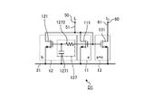
- FIG. 1 is a diagram showing a configuration of an amplifier circuit D1 according to the first embodiment.
- the amplifier circuit D1 is a single-ended amplifier.
- the amplifier circuit D1 includes a first circuit 11, a second circuit 12, a third circuit 13, a reference potential node 31, an input terminal 50, an input node 51, an output terminal 60, and an output node 61. ..
- a and b are parameters indicating the magnitude of the current flowing through the transistors of the first circuit 11 and the second circuit 12, respectively, and are parameters indicating the size of the transistor (hereinafter, referred to as “size parameter”). Call.).
- the size parameters a and b correspond to, for example, the number of fins of a FinFET (Fin Field Effect Transistor) and the gate width of a planar type transistor.
- the input node 51 includes wiring through which the input current I I flows.
- the output node 61 includes wiring through which the output current IO flows.
- the reference potential node 31 includes wiring to which the reference potential Vbase (for example, the ground potential) is supplied.
- the potential Vin of the input node 51 and the reference potential Vbase have a relationship of Vin> Vbase.
- the first circuit 11 has a first transistor 111.
- the first transistor 111 is, for example, an n-channel transistor, and is connected between the input node 51 through which the input current I I flows and the reference potential node 31.
- the gate electrode of the first transistor 111 is connected to the input node 51. Further, the drain electrode and the source electrode of the first transistor 111 are connected to the input node 51 and the reference potential node 31, respectively.
- the size parameter of the first transistor 111 is a.
- the first transistor 111 is an example of the first transistor.
- the second circuit 12 has a second transistor 121 and a low-pass filter circuit 127.
- the second transistor 121 is, for example, an n-channel transistor, and is connected in parallel with the first transistor 111 between the input node 51 through which the input current I I flows and the reference potential node 31.
- the gate electrode of the second transistor 121 is connected to the gate electrode of the first transistor 111 via a low-pass filter circuit 127. Further, the drain electrode and the source electrode of the second transistor 121 are connected to the input node 51 and the reference potential node 31, respectively.
- the size parameter of the second transistor 121 is b.
- the second transistor 121 is an example of the second transistor.
- the low-pass filter circuit 127 is a low-pass filter composed of a capacitor 1271 and a resistor 1272.
- the low-pass filter circuit 127 filters the signal to the gate electrode of the second transistor 121 in the high frequency band.
- the third circuit 13 has a third transistor 131.
- the third transistor 131 is, for example, an n-channel transistor, and is connected between the output node 61 through which the output current IO flows and the reference potential node 31.
- the gate electrode of the third transistor 131 is connected to the gate electrode of the first transistor 111.
- the size parameter of the third transistor 131 is a + b. That is, the size parameter a + b of the third transistor 131 is equal to the sum of the size parameter a of the first transistor 111 and the size parameter b of the second transistor 121.
- the third transistor 131 is an example of the third transistor.
- the first circuit 11 and the second circuit 12 form a current mirror circuit with the third circuit 13.
- the current I a + b at a ratio corresponding to the size parameter a + b of the third transistor 131 flows in the third circuit 13 at the mirror destination.
- FIG. 2 is a diagram showing the relationship between the DC gain, boost gain, peak gain and frequency of the amplifier circuit D1 according to the first embodiment.
- the DC gain corresponds to a gain that does not reflect the filtering operation of the low-pass filter circuit 127, and corresponds to a gain when the frequency of the input current I I is smaller than the cutoff frequency of the low-pass filter circuit 127.
- the peak gain corresponds to the gain reflecting the filtering operation of the low-pass filter circuit 127, and corresponds to the gain when the frequency of the input current I I is larger than the cutoff frequency of the low-pass filter circuit 127.
- a drain current I a + b flows through the third transistor 131 as a mirror current based on the current mirror operation.
- a current I a having a ratio corresponding to the size parameter a of the first transistor 111 flows through the first circuit 11.
- the gate electrode of the second transistor 121 is connected to the gate electrode of the first transistor 111 via the low-pass filter circuit 127.
- the gain (peak gain) when the frequency of the input current I I is larger than the cutoff frequency of the low-pass filter circuit 127 and the frequency of the input current I I are obtained from the cutoff frequency of the low-pass filter circuit 127.
- the difference from the gain (DC gain) when it is small can be determined according to the size parameter b of the second transistor 121.
- gm is the mutual conductance
- s is the variable of the Laplace transform
- CTOT is the value of the total capacity of the gate terminal.
- the amplifier circuit D1 includes the first circuit 11, the second circuit 12, and the third circuit 13.
- the first circuit 11 includes a first transistor 111 connected between an input node 51 through which an input current flows and a reference potential node 31 and having a gate electrode connected to the input node 51.
- the second circuit 12 includes a low-pass filter circuit 127.
- the second circuit 12 is connected in parallel with the first transistor 111 between the input node 51 and the reference potential node 31, and the gate electrode is connected to the gate electrode of the first transistor 111 via the low pass filter circuit 127.
- the third circuit 13 includes a third transistor 131 connected between the output node 61 through which the output current flows and the reference potential node 31 and having the gate electrode connected to the first transistor 111.
- the input signal input to the gate electrode of the second transistor 121 is filtered by the low-pass filter circuit 127. Therefore, in the high frequency band, it is possible to suppress the current I b from flowing through the second transistor 121, and the amplification factor can be increased from the DC gain to the peak gain.
- the amplifier circuit D1 does not require an inductor element (coil). Therefore, the circuit area can be reduced and the power consumption can be reduced as compared with the conventional amplifier circuit using the inductor element (coil).
- the amplifier circuit D1 is based on the current mirror circuit manufactured by the same process.
- input and output variation factors for example, parameters such as transistor threshold Vth and gain coefficient ⁇
- these variation factors cancel each other out due to the same change, and finally an amplifier circuit with a small gain error can be realized.
- the DC gain and the boost gain are varied by using a resistor (resistance value RS ), a capacitor (capacity CS ), an inductor parasitic resistance (resistance value RP ), and a load resistance (resistance value RL).
- the amplification factor A i of the amplifier circuit D1 which is based on current mirror circuit, as shown below, can be achieved linearity.
- I out ( ⁇ out / 2) V od 2 (3)
- the amplification factor A i of the amplifier circuit D1 is expressed by the following equation (5), the linear.
- a i ( ⁇ out / ⁇ in ) (5)
- FIG. 3 is a diagram showing the configuration of the amplifier circuit D2 according to the second embodiment.
- the amplifier circuit D2 includes, in addition to the configuration of the amplifier circuit D1 shown in FIG. 1, a constant current source 40 which outputs a current I c of the ratio corresponding to the size parameter c to the input node 51 side Have more.
- the constant current source 40 is connected in parallel with the first transistor 111 and the second transistor 121 between the input node 51 and the reference potential node 31.
- the size parameter of the third transistor 131 is a + b + c on the output node 61 side in response to the addition of the constant current source 40.
- FIG. 4 is a diagram showing the relationship between the DC gain, boost gain, peak gain and frequency of the amplifier circuit D2 according to the second embodiment. The operation of the amplifier circuit D2 will be described with reference to FIGS. 3 and 4.
- the third circuit 13, the first circuit 11, the second circuit 12, and the constant current source 40 operate as a current mirror circuit.
- the current I a + b + c at a ratio corresponding to the size parameter a + b + c of the third transistor 131 flows in the third circuit 13 at the mirror destination.
- the drain current I a + b + c flows through the third transistor 131 at the mirror destination based on the current mirror operation.
- a current I a having a ratio corresponding to the size parameter a of the first transistor 111 flows through the first circuit 11.
- the current I b does not flow in the second transistor 121.
- the amplifier circuit D2 according to the second embodiment, not only the boost gain but also the DC gain can be amplified. Further, by adjusting the current I c outputted by the constant current source 40, it is possible to amplify the boost gain and DC gain variably. Further, the boost gain can be further amplified as compared with the amplifier circuit D1 according to the first embodiment.
- FIG. 5 is a diagram showing the configuration of the amplifier circuit D3 according to the third embodiment.
- the amplifier circuit D3 is a differential amplifier that inputs input currents I IP and I IN from input terminals 50 and 52 and outputs output currents I OP and I ON from output terminals 60 and 62. be.
- the amplifier circuit D3 includes a first circuit 11, a second circuit 12, a third circuit 13, a fourth circuit 14, a fifth circuit 15, a sixth circuit 16, a seventh circuit 17, an eighth circuit 18, an input node 51, and a reference. It has a potential node 31 and an output node 61.
- the first circuit 11 and the second circuit 12 are as described in the first embodiment. Further, the size parameters of the third transistor 131 included in the third circuit 13 are the size parameter a of the first transistor 111, the size parameter b of the second transistor 121, and the size parameter c of the seventh transistor 171 included in the seventh circuit 17. Is equal to the sum of. That is, the size parameter of the third transistor 131 is a + b + c.
- the fourth circuit 14 has a fourth transistor 141.
- the fourth transistor 141 is, for example, an n-channel transistor, and is connected between the input node 32 through which the input current I IN flows and the reference potential node 31.
- the gate electrode of the fourth transistor 141 is connected to the input node 32.
- the drain electrode and the source electrode of the fourth transistor 141 are connected to the input node 32 and the reference potential node 31, respectively.
- the size parameter of the fourth transistor 141 is a.
- the fifth circuit 15 has a fifth transistor 151 and a low-pass filter circuit 157.
- the fifth transistor 151 is, for example, an n-channel transistor, and is connected in parallel with the fourth transistor 141 between the input node 32 through which the input current I IN flows and the reference potential node 31.
- the gate electrode of the fifth transistor 151 is connected to the fourth transistor 141 via a low-pass filter circuit 157. Further, the drain electrode and the source electrode of the fifth transistor 151 are connected to the input node 32 and the reference potential node 31, respectively.
- the size parameter of the fifth transistor 151 is b.
- the low-pass filter circuit 157 has a capacitor 1571 and a resistor 1572.
- the function of the low-pass filter circuit 157 is the same as that of the low-pass filter circuit 127.
- the sixth circuit 16 has a sixth transistor 161.
- the sixth transistor 161 is, for example, an n-channel transistor, and is connected between the output node 63 through which the output current ION flows and the reference potential node 31.
- the gate electrode of the sixth transistor 161 is connected to the gate electrode of the fourth transistor 141. Further, the drain electrode and the source electrode of the sixth transistor 161 are connected to the output node 63 and the reference potential node 31, respectively.
- the size parameter of the sixth transistor 161 is equal to the sum of the size parameter a of the fourth transistor 141, the size parameter b of the fifth transistor 151, and the size parameter c of the eighth transistor 181 of the eighth circuit 18. That is, the size parameter of the sixth transistor 161 is a + b + c.
- the seventh circuit 17 has a seventh transistor 171.
- the seventh transistor 171 is, for example, an n-channel transistor, and is connected between the input node 53 through which the input current I IN flows and the reference potential node 31. Further, the gate electrode of the 7th transistor 171 is connected to the gate electrode of the 1st transistor 111.
- the size parameter of the seventh transistor 171 is c.
- the eighth circuit 18 has an eighth transistor 181.
- the eighth transistor 181 is, for example, an n-channel transistor, and is connected between the input node 51 through which the input current IP flows and the reference potential node 31. Further, the gate electrode of the 8th transistor 181 is connected to the gate electrode of the 4th transistor 141.
- the size parameter of the eighth transistor 181 is c.
- the first circuit 11, the second circuit 12, the third circuit 13, and the seventh circuit 17 input the input currents I IP and I IN from the input terminals 50 and 52, and output the output current I OP from the output terminal 60. 1 Operates as a current mirror circuit CM1.
- the first current mirror circuit CM1 and the second current mirror circuit CM2 are crossed by the seventh transistor 171 of the seventh circuit 17 that inputs the input current I IN and the eighth transistor 181 of the eighth circuit 18 that inputs the input current I IP. Being a couple.
- FIG. 6 is a diagram showing frequency characteristics related to the gain of the amplifier circuit D3 according to the third embodiment. The operation of the amplifier circuit D3 will be described with reference to FIGS. 5 and 6.
- the size parameter c of the seventh transistor 171 is set in the seventh circuit 17. current flows -I c ratios corresponding to.
- the voltage between the gate source is equal between the third transistor 131 and the first transistor 111, the second transistor 121, and the seventh transistor 171. Therefore, a drain current I a + b + c flows through the third transistor 131.
- the operation of the second current mirror circuit CM2 is substantially the same except that the input currents I IP and I IN whose polarities are reversed are input.
- the drain current I a + b + c flows through the third transistor 131 at the mirror destination based on the current mirror operation.
- a current I a having a ratio corresponding to the size parameter a of the first transistor 111 flows through the first circuit 11.
- the gate electrode of the second transistor 121 is connected to the gate electrode of the first transistor 111 via the low-pass filter circuit 127.
- the input signal to the gate electrode of the second transistor 121 is filtered by the low-pass filter circuit 127, so that the current I b does not flow through the second transistor 121.
- the operation of the second current mirror circuit CM2 is substantially the same except that the input currents I IP and I IN whose polarities are reversed are input.
- the amplifier circuit D3 includes the first circuit 11, the second circuit 12, the third circuit 13, the fourth circuit 14, the fifth circuit 15, the sixth circuit 16, and the seventh circuit 17. , Eighth circuit 18.
- the first circuit 11 includes a first transistor 111 connected between an input node 51 through which an input current I IP flows and a reference potential node 31 and having a gate electrode connected to the input node 51.
- the second circuit 12 includes a low-pass filter circuit 127.
- the second circuit 12 is connected in parallel with the first transistor 111 between the input node 51 and the reference potential node 31, and the gate electrode is connected to the gate electrode of the first transistor 111 via the low pass filter circuit 127.
- the third circuit 13 includes a third transistor 131 connected between the output node 61 through which the output current flows and the reference potential node 31 and having the gate electrode connected to the first transistor 111.
- the fourth circuit 14 includes a fourth transistor 141 connected between the input node 53 through which the input current I IN flows and the reference potential node 31, and the gate electrode is connected to the input node 53.
- the fifth circuit 15 includes a low-pass filter circuit 157.
- the fifth circuit 15 is connected in parallel with the fourth transistor 141 between the input node 53 and the reference potential node 31, and the gate electrode is connected to the gate electrode of the fourth transistor 141 via the low pass filter circuit 157.
- the sixth circuit 16 includes a sixth transistor 161 connected between the output node 63 through which the output current flows and the reference potential node 31 and having the gate electrode connected to the fourth transistor 141.
- the seventh circuit 17 includes a seventh transistor 171 connected between the input node 53 through which the input current I IN flows and the reference potential node 31, and the gate electrode is connected to the gate electrode of the first transistor 111.
- the eighth circuit 18 includes an eighth transistor 181 connected between the input node 51 through which the input current I IP flows and the reference potential node 31, and the gate electrode is connected to the gate electrode of the fourth transistor 141.
- the first circuit 11, the second circuit 12, the third circuit 13, and the seventh circuit 17 operate as the first current mirror circuit CM1, and the fourth circuit 14, the fifth circuit 15, the sixth circuit 16, and the eighth circuit 18 Operates as the second current mirror circuit CM2.
- the first current mirror circuit CM1 and the second current mirror circuit CM2 are cross-coupled by the seventh transistor 171 of the seventh circuit 17 and the eighth transistor 181 of the eighth circuit 18.
- the amplifier circuit D3 can have a function of amplifying the DC gain in addition to the boost gain amplification function described in the first embodiment.
- FIG. 7 is a diagram showing the configuration of the amplifier circuit D4 according to the fourth embodiment.
- the amplifier circuit D4 in addition to the configuration of the amplifier circuit D3 shown in FIG. 5, the amplifier circuit D4 further has constant current sources 40 and 41 corresponding to the size parameter d on the input nodes 51 and 53, respectively. ..
- the constant current source 40 is connected in parallel with the first transistor 111 and the second transistor 121 between the input node 51 and the reference potential node 31.
- the constant current source 41 is connected in parallel with the fourth transistor 141 and the fifth transistor 151 between the input node 53 and the reference potential node 31.
- the size parameters of the third transistor 131 and the sixth transistor 161 are a + b + c + d on the output nodes 61 and 63 side in response to the addition of the constant current sources 40 and 41.
- the DC gain can be further amplified as compared with the amplifier circuit D3, as in the case of the amplifier circuit D2 according to the second embodiment. Further, by adjusting the current I d outputted by the constant current source 40 and 41, it is possible to amplify the boost gain and DC gain variably.
- FIG. 8 is a diagram showing the configuration of the amplifier circuit D5 according to the fifth embodiment.
- the amplifier circuit D5 according to the fifth embodiment uses a transistor for on / off control inserted in the source side of each transistor included in the first current mirror circuit CM1 and the second current mirror circuit CM2, and has a size parameter a. , B, and c are individually controlled, and the DC gain and boost gain are variably amplified.
- the amplifier circuit D5 is a differential amplifier that inputs input currents I IP and I IN and outputs output currents I OP and I ON.
- the amplifier circuit D5 has A first circuits 11 (hereinafter referred to as "group of first circuits”) connected in parallel.
- the amplifier circuit D5 has B second circuits 12 (hereinafter referred to as "group of second circuits") connected in parallel.
- the amplifier circuit D5 has C seventh circuits 17 (hereinafter referred to as "group of seventh circuits") connected in parallel.
- the amplifier circuit D5 has A + B + C third circuits 13 (hereinafter referred to as "group of third circuits") connected in parallel.
- the number of the third circuit 13 included in the group of the third circuit is the number of the first circuit 11 included in the group of the first circuit, the number of the second circuit 12 included in the group of the second circuit, and the first. It is equal to the total number of 7th circuits 17 included in the group of 7 circuits.
- the amplifier circuit D5 has A fourth circuits 14 (hereinafter referred to as "group of fourth circuits") connected in parallel.
- the amplifier circuit D5 has B fifth circuits 15 (hereinafter referred to as "group of fifth circuits”) connected in parallel.
- the amplifier circuit D5 has C eighth circuits 18 (hereinafter referred to as "group of eighth circuits") connected in parallel.
- the amplifier circuit D5 has A + B + C sixth circuits 16 (hereinafter referred to as "group of sixth circuits") connected in parallel.
- the number of the sixth circuit included in the group of the sixth circuit is the number of the fourth circuit 14 included in the group of the fourth circuit, the number of the fifth circuit 15 included in the group of the fifth circuit, and the eighth. Equal to the sum of the number of eighth circuits 18 contained in the group of circuits.
- the group of the first circuit, the group of the second circuit, and the group of the seventh circuit constitute the group of the third circuit and the group of the first current mirror circuit CM1. Further, the group of the fourth circuit, the group of the fifth circuit, and the group of the sixth circuit constitute the group of the eighth circuit and the group of the second current mirror circuit CM2. Further, the amplifier circuit D5 has a controller 25.
- Each first circuit 11 has a ninth transistor 112 connected in series with the first transistor 111.
- the ninth transistor 112 is, for example, an n-channel transistor, and the drain electrode of the ninth transistor 112 is connected to the source electrode of the first transistor 111.
- the source electrode of the ninth transistor 112 is connected to the reference potential node 31.
- the gate electrode of the ninth transistor 112 is connected to a predetermined fixed potential node, for example, a power potential node.
- the size parameter of the first transistor 111 is "1".
- the A first transistors 111 connected in parallel in the group of the first circuit form a part of the group of transistors that carry a current I a at a ratio corresponding to the size parameter a.
- each second circuit 12 includes a tenth transistor 122 for on / off control, an eleventh transistor 123, and a twelfth transistor 124 for on / off control. It has 1 inverter 128.
- the tenth transistor 122 is, for example, an n-channel transistor, and is connected between the second transistor 121 and the reference potential node 31.
- the drain electrode of the tenth transistor 122 is connected to the source electrode of the second transistor 121.
- the source electrode of the tenth transistor 122 is connected to the reference potential node 31.
- the gate electrode of the tenth transistor 122 is connected to the first control node 33.
- the size parameter of the second transistor 121 is "1".
- the B second transistors 121 connected in parallel in the second circuit group form part of a group of transistors that, when turned on, carry a current I b at a ratio corresponding to the size parameter b. Is.
- the eleventh transistor 123 is, for example, an n-channel transistor, and is connected in parallel with the first transistor 111 and the second transistor 121 between the input node 51 and the reference potential node 31.
- the drain electrode of the 11th transistor 123 is connected to the input node 51.
- the source electrode of the 11th transistor 123 is connected to the drain electrode of the 12th transistor 124.
- the gate electrode of the eleventh transistor 123 is connected to the gate electrode of the first transistor 111 without passing through the low-pass filter circuit 127.
- the size parameter of the 11th transistor 123 is "1".
- the B eleventh transistors 123 connected in parallel in the second circuit group form a part of a group of transistors that, when turned on, carry a current I a at a ratio corresponding to the size parameter a. Is.
- the twelfth transistor 124 is, for example, an n-channel transistor, and is connected between the eleventh transistor 123 and the reference potential node 31.
- the source electrode of the twelfth transistor 124 is connected to the reference potential node 31.
- the input side of the first inverter 128 is connected to the gate electrode of the tenth transistor 122, that is, the first control node 33.
- the output side of the first inverter 128 is connected to the gate electrode of the twelfth transistor 124.
- the first inverter 128 selectively turns on one of the tenth transistor 122 and the twelfth transistor 124 according to the input control signal.
- the controller 25 supplies a control signal (for example, a high level signal) for turning on the tenth transistor 122 and passing a current through the second transistor 121 to the first control node 33.
- a control signal for example, a high level signal
- the tenth transistor 122 is turned on by the high level signal, and a current I 1 having a ratio corresponding to the size parameter “1” flows through the second transistor 121.
- the high level signal is also supplied to the first inverter 128.
- the first inverter 128 supplies a low-level signal obtained by inverting the supplied high-level signal to the gate electrode of the twelfth transistor 124.
- the twelfth transistor 124 is not turned on because the control signal supplied to the gate electrode is a low level signal.
- the controller 25 supplies a control signal (for example, a low level signal) for turning off the tenth transistor 122 to the first control node 33.
- a control signal for example, a low level signal
- the 10th transistor 122 is turned off by the low level signal, and the current I 1 does not flow through the second transistor 121.
- the low level signal is also supplied to the first inverter 128.
- the first inverter 128 supplies a high-level signal obtained by inverting the supplied low-level signal to the gate electrode of the twelfth transistor 124.
- Twelfth transistor 124 is turned on because the control signal supplied to the gate electrode is at a high level signal, the size parameter "1" a current flows I 1 of the ratio corresponding to the eleventh transistor 123.
- Each 7th circuit 17 has a 7th transistor 171 and a 13th transistor 172, a 14th transistor 173, a 15th transistor 174, and a second inverter 175.
- the seventh transistor 171 is, for example, an n-channel transistor, and is connected in parallel with the fourth transistor 141 and the fifth transistor 151 between the input node 53 and the reference potential node 31.
- the drain electrode of the seventh transistor 171 is connected to the input node 53.
- the source electrode of the 7th transistor 171 is connected to the drain electrode of the 13th transistor 172.
- the gate electrode of the seventh transistor 171 is connected to the gate electrode of the first transistor 111.
- the size parameter of the 7th transistor 171 is "1".
- C-number of the seventh transistor 171 are connected in parallel, if it is turned on, constitutes a part of the group of transistors to flow a current -I c ratio corresponding to the size parameter c It is a thing.
- the 13th transistor 172 is, for example, an n-channel transistor, and is connected between the 7th transistor 171 and the reference potential node 31.
- the source electrode of the thirteenth transistor 172 is connected to the reference potential node 31.
- the 14th transistor 173 is, for example, an n-channel transistor, and is connected in parallel with the first transistor 111 and the second transistor 121 between the input node 51 and the reference potential node 31.
- the drain electrode of the 14th transistor 173 is connected to the input node 51.
- the source electrode of the 14th transistor 173 is connected to the drain electrode of the 15th transistor 174.
- the gate electrode of the 14th transistor 173 is connected to the gate electrode of the first transistor 111.
- the size parameter of the 14th transistor 173 is "1".
- the C 14th transistors 173 connected in parallel in the 7th circuit group constitute a part of the group of transistors that, when turned on, carry a current I a at a ratio corresponding to the size parameter a. Is.
- the 15th transistor 174 is, for example, an n-channel transistor, and is connected between the 14th transistor 173 and the reference potential node 31.
- the source electrode of the 15th transistor 174 is connected to the reference potential node 31.
- the gate electrode of the 15th transistor 174 is connected to the second control node 34.
- the input side of the second inverter 175 is connected to the gate electrode of the 15th transistor 174, that is, the second control node 34.
- the output side of the second inverter 175 is connected to the gate electrode of the thirteenth transistor 172.
- the second inverter 175 selectively turns on either the 13th transistor 172 or the 15th transistor 174 according to the input control signal.
- the controller 25 supplies a high-level signal for turning on the fifteenth transistor 174 and passing a current through the fourteenth transistor 173 to the second control node 34.
- the 15th transistor 174 is turned on by the high level signal, and a current I 1 having a ratio corresponding to the size parameter “1” flows through the 14th transistor 173.
- the high level signal is also supplied to the second inverter 175.
- the second inverter 175 supplies a low-level signal obtained by inverting the supplied high-level signal to the gate electrode of the thirteenth transistor 172.
- the thirteenth transistor 172 is not turned on because the control signal supplied to the gate electrode is a low level signal.
- the controller 25 supplies a low level signal for turning off the 14th transistor 173 to the second control node 34.
- the 15th transistor 174 is turned off by the low level signal, and the current I 1 does not flow through the 14th transistor 173.
- the low level signal is also supplied to the second inverter 175.
- the second inverter 175 supplies a high-level signal obtained by inverting the supplied low-level signal to the gate electrode of the thirteenth transistor 172. Thirteenth transistor 172 is turned on because the control signal supplied to the gate electrode is at a high level signal, the size parameter "1" a current flows -I 1 ratio corresponding to the seventh transistor 171.
- Each third circuit 13 has a 16th transistor 132 connected between the 3rd transistor 131 and the reference potential node 31.
- the 16th transistor 132 is, for example, an n-channel transistor, and the drain electrode of the 16th transistor 132 is connected to the source electrode of the 3rd transistor 131.
- the source electrode of the 16th transistor 132 is connected to the reference potential node 31.
- the gate electrode of the 16th transistor 132 is connected to a predetermined fixed potential node, for example, a power potential node.
- the size parameter of the third transistor 131 is "1".
- the A + B + C third transistors 131 connected in parallel in the third circuit group constitute a group of transistors that carry a current I a + b + c at a ratio corresponding to the size parameter a + b + c.
- the first transistor 111, the second transistor 121, the third transistor 131, the seventh transistor 171 and the eleventh transistor 123, and the 14th transistor 173 have the sizes thereof.
- the parameters are all "1" and the sizes are equal to each other.
- Each fourth circuit 14 has a 17th transistor 142 connected between the 4th transistor 141 and the reference potential node 31.
- the 17th transistor 142 is, for example, an n-channel transistor, and the drain electrode of the 17th transistor 142 is connected to the source electrode of the 4th transistor 141.
- the source electrode of the 17th transistor 142 is connected to the reference potential node 31.
- the gate electrode of the 17th transistor 142 is connected to a predetermined fixed potential node, for example, a power potential node.
- the size parameter of the fourth transistor 141 is "1".
- the A fourth transistor 141 connected in parallel in the fourth circuit group constitutes a part of the group of transistors that carry a current ⁇ Ia at a ratio corresponding to the size parameter a.
- Each fifth circuit 15 has an 18th transistor 152, a 19th transistor 153, a 20th transistor 154, and a third inverter 158 in addition to the 5th transistor 151 and the low-pass filter circuit 157.
- the 18th transistor 152 is, for example, an n-channel transistor, and is connected between the 5th transistor 151 and the reference potential node 31.
- the drain electrode of the 18th transistor 152 is connected to the source electrode of the 5th transistor 151.
- the source electrode of the 18th transistor 152 is connected to the reference potential node 31.
- the gate electrode of the 18th transistor 152 is connected to the third control node 35.
- the size parameter of the fifth transistor 151 is "1".
- the B fifth transistors 151 connected in parallel in the fifth circuit group form part of a group of transistors that, when turned on, carry a current ⁇ I b at a ratio corresponding to the size parameter b. It is a thing.
- the 19th transistor 153 is, for example, an n-channel transistor, and is connected in parallel with the 4th transistor 141 and the 5th transistor 151 between the input node 53 and the reference potential node 31.
- the drain electrode of the 19th transistor 153 is connected to the input node 53.
- the source electrode of the 19th transistor 153 is connected to the drain electrode of the 20th transistor 154.
- the gate electrode of the 19th transistor 153 is connected to the gate electrode of the 4th transistor 141 without passing through the low-pass filter circuit 157.
- the size parameter of the 19th transistor 153 is "1".
- the B 19th transistors 153 connected in parallel in the fifth circuit group form part of a group of transistors that, when turned on, carry a current ⁇ Ia at a ratio corresponding to the size parameter a. It is a thing.
- the 20th transistor 154 is, for example, an n-channel transistor, and is connected between the 19th transistor 153 and the reference potential node 31.
- the source electrode of the 20th transistor 154 is connected to the reference potential node 31.
- the input side of the third inverter 158 is connected to the gate electrode of the 18th transistor 152, that is, the third control node 35.
- the output side of the third inverter 158 is connected to the gate electrode of the 20th transistor 154.
- the third inverter 158 selectively turns on either the 18th transistor 152 or the 20th transistor 154 according to the input control signal.
- Each 8th circuit 18 has an 8th transistor 181 and a 21st transistor 182, a 22nd transistor 183, a 23rd transistor 184, and a 4th inverter 185.
- the eighth transistor 181 is, for example, an n-channel transistor, and is connected in parallel with the first transistor 111 and the second transistor 121 between the input node 51 and the reference potential node 31.
- the drain electrode of the eighth transistor 181 is connected to the input node 51.
- the source electrode of the eighth transistor 181 is connected to the drain electrode of the 21st transistor 182.
- the gate electrode of the eighth transistor 181 is connected to the gate electrode of the fourth transistor 141.
- the size parameter of the eighth transistor 181 is "1".
- C-number of the eighth transistor 181 are connected in parallel, if it is turned on, constitutes a part of the group of transistors to flow a current I c of the ratio corresponding to the size parameter c Is.
- the 21st transistor 182 is, for example, an n-channel transistor, and is connected between the 8th transistor 181 and the reference potential node 31.
- the source electrode of the 21st transistor 182 is connected to the reference potential node 31.
- the 22nd transistor 183 is, for example, an n-channel transistor, and is connected in parallel with the 4th transistor 141 and the 5th transistor 151 between the input node 53 and the reference potential node 31.
- the drain electrode of the 22nd transistor 183 is connected to the input node 53.
- the source electrode of the 22nd transistor 183 is connected to the drain electrode of the 23rd transistor 184.
- the gate electrode of the 22nd transistor 183 is connected to the gate electrode of the 4th transistor 141.
- the size parameter of the 22nd transistor 183 is "1".
- the size parameter of the 22nd transistor 183 is "1".
- the C 22nd transistors 183 connected in parallel in the group of eighth circuits form part of a group of transistors that, when turned on, carry a current ⁇ I a at a ratio corresponding to the size parameter a. It is a thing.
- the 23rd transistor 184 is, for example, an n-channel transistor, and is connected between the 22nd transistor 183 and the reference potential node 31.
- the source electrode of the 23rd transistor 184 is connected to the reference potential node 31.
- the gate electrode of the 23rd transistor 184 is connected to the 4th control node 36.
- the input side of the 4th inverter 185 is connected to the gate electrode of the 23rd transistor 184, that is, the 4th control node 36.
- the output side of the fourth inverter 185 is connected to the gate electrode of the 21st transistor 182.
- the fourth inverter 185 selectively turns on either the 21st transistor 182 or the 23rd transistor 184 according to the input control signal.
- Each sixth circuit 16 has a 24th transistor 162 connected between the 6th transistor 161 and the reference potential node 31.
- the 24th transistor 162 is, for example, an n-channel transistor, and the drain electrode of the 24th transistor 162 is connected to the source electrode of the 6th transistor 161.
- the source electrode of the 24th transistor 162 is connected to the reference potential node 31.
- the gate electrode of the 24th transistor 162 is connected to a predetermined fixed potential node, for example, a power potential node.
- the size parameter of the sixth transistor 161 is "1".
- the A + B + C sixth transistors 161 connected in parallel in the sixth circuit group constitute a part of the group of transistors that carry a current ⁇ I a + b + c at a ratio corresponding to the size parameter a + b + c.
- the fourth transistor 141, the fifth transistor 151, the sixth transistor 161 and the eighth transistor 181, the 19th transistor 153, and the 22nd transistor 183 have size parameters thereof. Are all "1" and the sizes are equal to each other.
- the controller 25 selectively inputs a plurality of first control signals to the group of the second circuit and selectively inputs the plurality of second control signals to the group of the seventh circuit according to the set DC gain and boost gain.
- This is a control circuit that variably performs input, selective input of a plurality of third control signals to a group of fifth circuits, and selective input of a plurality of fourth control signals to a group of eighth circuits.
- the difference in gain between the case where the frequency ⁇ of the input currents I IP and I IN is larger and smaller than the cutoff frequency ⁇ z of the low-pass filter circuit 127 and the low-pass filter circuit 157 is the first. It is determined according to the number of second transistors 121 turned on by one control signal and the number of fifth transistors 151 turned on by a third control signal.
- the gain when the frequency ⁇ of the input currents I IP and I IN is smaller than the cutoff frequency ⁇ z of the low-pass filter circuit 127 and the low-pass filter circuit 157 is turned on by the second control signal. It is determined according to the number of 7 transistors 171 and the number of 8th transistors 181 turned on by the 4th control signal.
- the amplifier circuit D5 is input current I IP, the gain when the frequency of the I IN omega is greater than the cut-off frequency omega z of the low-pass filter circuit 127 and the low-pass filter circuit 157, the input current I IP, the I IN It is larger than the gain when the frequency ⁇ is smaller than the cutoff frequency ⁇ z of the low-pass filter circuit 127 and the low-pass filter circuit 157.
- the controller 25 has a plurality of first control nodes 33, a plurality of second control nodes 34, a plurality of third control nodes 35, and a plurality of third control nodes, depending on the DC gain and boost gain to be set.
- a corresponding control signal is supplied to the fourth control node 36.
- the controller 25 stores a look-up table for determining the size parameters a, b, c based on the set DC gain and boost gain.
- the controller 25 determines the values of the size parameters a, b, and c based on the set DC gain and boost gain and the look-up table.
- the controller 25 outputs the corresponding control signals for setting the determined values of the size parameters a, b, and c to the plurality of first control nodes 33, the plurality of second control nodes 34, and the plurality of third control nodes 35. And supply to the fourth control node 36.
- This switching control is performed using the size parameters a, b, c determined based on the level of DC gain and the level of boost gain.
- the size parameters a, b, and c use DC gain and boost gain as input information, and the respective values of the size parameters a, b, and c (that is, in the first current mirror circuit CM1, the current of the ratio corresponding to each size parameter is used.
- the number of transistors to be driven to flow) is used as output information and is determined using a lookup table.
- FIGS. 9A, 9B, and 9C are look-up tables for determining the size parameters a, b, and c based on the set DC gain and boost gain.
- EQ means the level of boost gain
- VGA means the level of DC gain.
- a control signal for example, a high level signal
- a control signal for example, a low level signal for turning on the 12th transistor 124 and passing a current through the 11th transistor 123 is supplied to the first control node 33.
- a control signal for example, a low level signal
- a control signal for example, a low level signal
- a control signal for example, a high level signal for turning on the 15th transistor 174 and passing a current through the 14th transistor 173 is not supplied.
- the second transistor 121 whose size parameter is “1" is turned on for the three second circuits 12 out of the 14 second circuits 12, and the remaining 11 second circuits 12 are controlled.
- the circuit 12 is controlled to turn on the eleventh transistor 123 whose size parameter is “1”.
- the 7th transistor 171 whose size parameter is "1" is turned on for the 10 7th circuits 17 out of the 10 7th circuits 17, and the 10th 7th circuits 17 are controlled.
- the 14th transistor 173 whose size parameter is "1" is controlled so that none of them is turned on.
- the size parameters a, b, and c may be determined at any time. For example, it can be performed at the time of starting the device on which the amplifier circuit D5 is mounted.
- the amplifier circuit D5 by setting the desired DC gain and boost gain (peak gain), the size parameter a for realizing the setting by the look-up table. , B, c can be determined automatically.
- the amplifier circuit D5 can execute switching control according to the determined size parameters a, b, and c to amplify the DC gain and the boost gain.
- the user can set the DC gain and the boost gain individually and variably. This makes it possible to further cope with the increase in the signal amplitude level.
- the amplifier circuit D6 according to the sixth embodiment is for connecting any one of the amplifier circuits D1 to D5 in multiple stages to realize a larger DC gain and boost gain.
- FIG. 10 is a diagram showing the configuration of the amplifier circuit D6 according to the sixth embodiment, and illustrates a case where the amplifier circuit D3 is connected in two stages.
- the output node of the amplifier circuit D3 configured by the n-channel transistor is connected to the input node of the amplifier circuit D3'configured by replacing the n-channel transistor of the amplifier circuit D3 with the p-channel transistor. Two-stage connection is realized.
- FIG. 11 is a diagram showing the configuration of the receiving circuit D7 according to the seventh embodiment.
- the receiving circuit D7 includes a CTLE 81, a DFE (Decision feedback equalizer) 82, and a DEMUX (Demultiplexer) 83.
- CTLE 81 CTLE
- DFE Decision feedback equalizer
- DEMUX Demultiplexer
- the CTLE 81 has each amplifier circuit according to the first to sixth embodiments inside, and is continuously on the time axis with respect to the differential input signal (serial input signal) received by the differential input terminals 84 and 85. It is an input amplification circuit that performs amplification processing and equalization processing.
- the DFE 82 is an equalization circuit that receives the output signal of the CTLE 81 and performs equalization processing by a feedback loop and determination of the signal level for the output signal of the CTLE 81. Note that CTLE81 and DFE82 are examples of input circuits.
- the DEMUX83 is a conversion circuit that receives the output signal of the DFE82 and performs a conversion process of converting the output signal of the DFE82 from serial to parallel.
- FIG. 12 is a diagram showing the configuration of the semiconductor integrated circuit D8 according to the eighth embodiment. As shown in FIG. 12, the semiconductor integrated circuit D8 has a processing circuit 7 that executes predetermined signal processing on the output signals of the receiving circuit 80 and the receiving circuit 80.
- the receiving circuit 80 is, for example, the receiving circuit D7 shown in FIG. 11, and the CTLE 81 in the receiving circuit 80 has each amplifier circuit according to the first to sixth embodiments inside.
- a first circuit including a first transistor connected between an input node through which an input current flows and a reference potential node and a gate electrode connected to the input node.
- a second unit that includes a low-pass filter circuit, is connected in parallel with the first transistor between the input node and the reference potential node, and the gate electrode is connected to the gate electrode of the first transistor via the low-pass filter circuit.
- the second circuit including the transistor and A third circuit including a third transistor connected between the output node through which the output current flows and the reference potential node and the gate electrode connected to the gate electrode of the first transistor.
- Appendix 2 The amplifier circuit according to Appendix 1, wherein the first circuit and the second circuit constitute the third circuit and a current mirror circuit.
- the low-pass filter circuit is A capacitor connected between the gate electrode of the second transistor and the reference potential node,
- the amplifier circuit according to Appendix 1 or 2 which includes a resistor connected between the gate electrode of the second transistor and the gate electrode of the first transistor.
- Appendix 5 The amplifier circuit according to Appendix 4, wherein the first transistor, the second transistor, and the third transistor are planar transistors, respectively, and the size corresponds to the gate width of the planar transistor.
- Appendix 8 The amplifier circuit according to Appendix 7, wherein the gain of the amplifier circuit when the frequency of the input current is smaller than the cutoff frequency of the low-pass filter circuit is determined according to the size of the current source.
- Appendix 10 The amplification according to Appendix 9, wherein the difference in gain of the amplifier circuit between the case where the frequency of the input current is larger than the cutoff frequency of the low-pass filter circuit and the case where the frequency is smaller than the cutoff frequency of the low-pass filter circuit is determined according to the size of the second transistor. circuit.
- a first circuit including a first transistor connected between a first input node through which a first input current flows and a reference potential node and a gate electrode connected to the first input node.
- a first low-pass filter circuit is included, connected in parallel with the first transistor between the first input node and the reference potential node, and a gate electrode is interposed via the gate electrode of the first transistor and the first low-pass filter circuit.
- the second circuit including the second transistor connected by A third circuit including a third transistor connected between the first output node through which the first output current flows and the reference potential node and the gate electrode connected to the gate electrode of the first transistor.
- a fourth circuit including a fourth transistor connected between the second input node through which the second input current flows and the reference potential node and the gate electrode connected to the second input node.
- a second low-pass filter circuit is included, connected in parallel with the fourth transistor between the second input node and the reference potential node, and a gate electrode is interposed via the gate electrode of the fourth transistor and the second low-pass filter circuit.
- the fifth circuit including the fifth transistor connected by A sixth circuit including a sixth transistor connected between the second output node through which the second output current flows and the reference potential node and the gate electrode connected to the gate electrode of the fourth transistor.
- a seventh circuit including a seventh transistor connected between the second input node and the reference potential node and having a gate electrode connected to the gate electrode of the first transistor.
- An eighth circuit including an eighth transistor connected between the first input node and the reference potential node and having a gate electrode connected to the gate electrode of the fourth transistor.
- the first circuit, the second circuit, and the seventh circuit constitute the third circuit and the first current mirror circuit.
- the differential amplifier circuit according to Appendix 11 wherein the fourth circuit, the fifth circuit, and the eighth circuit constitute the sixth circuit and the second current mirror circuit.
- the first low-pass filter circuit is A first capacitor connected between the gate electrode of the second transistor and the reference potential node, It includes a first resistor connected between the gate electrode of the second transistor and the gate electrode of the first transistor.
- the second low-pass filter circuit is A second capacitor connected between the gate electrode of the fifth transistor and the reference potential node,
- the size of the third transistor is equal to the sum of the size of the first transistor, the size of the second transistor, and the size of the seventh transistor.
- the second circuit is connected in parallel with the tenth transistor connected between the second transistor and the reference potential node, and the second transistor between the first input node and the reference potential node, and is gated.
- the eleventh transistor whose electrodes are connected to the gate of the first transistor without passing through the first low-pass filter circuit, the twelfth transistor connected between the eleventh transistor and the reference potential node, and the tenth transistor.
- One of the input side and the output side is connected to the gate electrode of the transistor, the other of the input side and the output side is connected to the gate electrode of the twelfth transistor, and the tenth is corresponding to the input first control signal.
- the seventh circuit has a transistor and a first inverter that selectively transitions one of the twelfth transistors to ON.
- the seventh circuit is connected in parallel with the thirteenth transistor connected between the seventh transistor and the reference potential node, and the seventh transistor between the first input node and the reference potential node, and is gated.
- the 14th transistor whose electrodes are connected to the gate of the 1st transistor, the 15th transistor connected between the 14th transistor and the reference potential node, and the input side and output side to the gate electrode of the 15th transistor.
- One of the 13th transistor and the other of the output side are connected to the gate electrode of the 13th transistor, and either the 13th transistor or the 15th transistor is connected according to the input second control signal.
- the fifth circuit is connected in parallel with the eighteenth transistor connected between the fifth transistor and the reference potential node, and the fifth transistor between the second input node and the reference potential node, and is gated.
- the 19th transistor whose electrodes are connected to the gate of the 4th transistor without passing through the 2nd low-pass filter circuit, the 20th transistor connected between the 19th transistor and the reference potential node, and the 18th transistor.
- One of the input side and the output side is connected to the gate electrode of the transistor, and the other side of the input side and the output side is connected to the gate electrode of the 20th transistor. It has a transistor and a third inverter that selectively transitions either one of the 20th transistors to ON.
- the eighth circuit is connected in parallel with the 21st transistor connected between the 8th transistor and the reference potential node, and in parallel with the 8th transistor between the 2nd input node and the reference potential node, and is a gate.
- the 22nd transistor whose electrode is connected to the gate of the 4th transistor, the 23rd transistor connected between the 22nd transistor and the reference potential node, and one of the input sides to the gate electrode of the 23rd transistor
- the other of the input side and the output side is connected to the gate electrode of the 21st transistor, and either the 21st transistor or the 23rd transistor is selectively selected according to the input 4th control signal.
- the group of 7 circuits constitutes the group of the 3rd circuit including the 3rd circuit connected in parallel and the 1st current mirror circuit.
- the group of circuits constitutes the group of the sixth circuit including the sixth circuit connected in parallel and the second current mirror circuit.
- a control circuit that variably performs a plurality of selective inputs of the third control signal to the group of the fifth circuit and a plurality of selective inputs of the fourth control signal to the group of the eighth circuit.
- the differential amplifier circuit according to Appendix 15, including the above.
- the DC gain is the gain of the amplifier circuit when the frequency of the input current is smaller than the cutoff frequency of the low-pass filter circuit.
- the differential amplifier circuit according to Appendix 16 wherein the boost gain is a gain of the amplifier circuit when the frequency of the input current is larger than the cutoff frequency of the low-pass filter circuit.
- the number of the third circuit included in the group of the third circuit is the number of the first circuit included in the group of the first circuit, the number of the second circuit included in the group of the second circuit, and the number of the second circuit. Equal to the total number of 7th circuits included in the 7th circuit group, The number of the sixth circuit included in the group of the sixth circuit is the number of the fourth circuit included in the group of the fourth circuit, the number of the fifth circuit included in the group of the fifth circuit, and the number of the fifth circuit.
- the differential amplifier circuit according to Appendix 16 or 17, which is equal to the total number of the eighth circuits included in the group of the eighth circuits.
- Appendix 24 The difference described in Appendix 23, wherein the gain of the amplifier circuit when the frequency of the input current is smaller than the cutoff frequency of the low-pass filter circuit is determined according to the sizes of the first current source and the second current source. Dynamic amplifier circuit.
- Appendix 28 The receiving circuit described in Appendix 27 and A semiconductor integrated circuit having a processing circuit that executes predetermined signal processing with respect to the output signal of the receiving circuit.
- the amplifier circuit, the differential amplifier circuit, the receiver circuit, and the semiconductor integrated circuit according to the embodiment disclosed in the present specification have a boost gain amplification function and a small area while maintaining the linearity of the gain. Realize.
Landscapes
- Engineering & Computer Science (AREA)
- Power Engineering (AREA)
- Microelectronics & Electronic Packaging (AREA)
- Physics & Mathematics (AREA)
- Nonlinear Science (AREA)
- Electromagnetism (AREA)
- General Physics & Mathematics (AREA)
- Radar, Positioning & Navigation (AREA)
- Automation & Control Theory (AREA)
- Amplifiers (AREA)
Abstract
The amplification circuit according to an embodiment has a first circuit, a second circuit, and a third circuit. The first circuit includes a first transistor connected between a reference potential node and an input node through which an input current is channeled, the gate electrode of the first transistor being connected to the input node. The second circuit includes a low-pass filter circuit, and includes a second transistor connected between the input node and the reference potential node so as to be parallel to the first transistor, the gate electrode of the second transistor being connected, via the low-pass filter circuit, to the gate electrode of the first transistor. The third circuit includes a third transistor connected between the reference potential node and an output node through which an output current is channeled, the gate electrode of the third transistor being connected to the gate of the first transistor.
Description
本明細書等に開示の一実施形態は、例えば、CTLE(Continuous Time Linear Equalizer、連続時間線形等化器)に用いられる増幅回路、差動増幅回路、受信回路及び半導体集積回路に関する。
One embodiment disclosed in the present specification and the like relates to, for example, an amplifier circuit, a differential amplifier circuit, a receiver circuit, and a semiconductor integrated circuit used in a CTLE (Continuous Time Liner Equalizer, continuous time linear equalizer).
CTLEは、ネットワークやデータセンタ向けの高速インターフェース等に用いられるSerDes(SERializer DESerializer)受信回路の入力増幅回路であり、伝送路でのロス補償回路として用いられる。従来のCTLEは、ソースデジェネレーション型イコライザを用いている。
CTLE is an input amplifier circuit of a SerDes (SERializer DESerializer) receiving circuit used for a high-speed interface for a network or a data center, and is used as a loss compensation circuit in a transmission line. The conventional CTLE uses a source degeneration type equalizer.
しかしながら、ソースデジェネレーション型イコライザを用いる従来のCTLEは、インダクタ素子(コイル)を用いてブーストゲイン増幅機能を実現する。このため、回路サイズ(面積)が大きくなる。また、回路内の抵抗、相互コンダクタンスなどのばらつき要素により、ゲインが非線形となる。
However, the conventional CTLE using the source degeneration type equalizer realizes the boost gain amplification function by using the inductor element (coil). Therefore, the circuit size (area) becomes large. In addition, the gain becomes non-linear due to variation factors such as resistance and mutual conductance in the circuit.
近年では、CMOSテクノロジの微細化により、CTLEの更なる低電力化と小面積化が要求される。また、信号振幅レベルの多値化により、高い線形性が必要とされる。
In recent years, due to the miniaturization of CMOS technology, further reduction in power consumption and area of CTLE is required. In addition, high linearity is required due to the multi-valued signal amplitude level.
本明細書等に開示の実施形態が解決しようとする課題の一つは、ゲインの線形性を維持しつつ、ブーストゲイン増幅機能及び小面積化を実現する増幅回路、差動増幅回路、受信回路及び半導体集積回路を提供することである。
One of the problems to be solved by the embodiments disclosed in the present specification and the like is an amplifier circuit, a differential amplifier circuit, and a receiving circuit that realize a boost gain amplification function and a small area while maintaining the linearity of the gain. And to provide semiconductor integrated circuits.
実施形態に係る増幅回路は、入力電流が流れる入力ノードと基準電位ノードの間に接続され、ゲート電極が前記入力ノードと接続された第1トランジスタを含む第1回路と、ローパスフィルタ回路を含み、前記入力ノードと前記基準電位ノードの間において前記第1トランジスタと並列に接続され、ゲート電極が前記第1トランジスタのゲートと前記ローパスフィルタ回路を介して接続された第2トランジスタを含む第2回路と、出力電流が流れる出力ノードと前記基準電位ノードの間に接続され、ゲート電極が前記第1トランジスタのゲートと接続された第3トランジスタを含む第3回路と、を有する。
The amplifier circuit according to the embodiment includes a first circuit including a first transistor connected between an input node through which an input current flows and a reference potential node, and a gate electrode connected to the input node, and a low-pass filter circuit. A second circuit including a second transistor connected in parallel with the first transistor between the input node and the reference potential node and having a gate electrode connected to the gate of the first transistor via the low pass filter circuit. It has a third circuit including a third transistor connected between the output node through which the output current flows and the reference potential node and the gate electrode connected to the gate of the first transistor.
本明細書に開示の一実施形態によれば、ゲインの線形性を維持しつつ、ブーストゲイン増幅機能及び小面積化を実現する増幅回路、差動増幅回路、受信回路及び半導体集積回路を実現することができる。
According to one embodiment disclosed herein, an amplifier circuit, a differential amplifier circuit, a receiver circuit, and a semiconductor integrated circuit that realize a boost gain amplification function and a small area while maintaining gain linearity are realized. be able to.
以下に添付図面を参照して、実施形態に係る増幅回路、差動増幅回路、受信回路及び半導体集積回路を詳細に説明する。なお、この実施形態により本発明が限定されるものではない。また、以下の説明において、各図面で共通する部分には同一の符号を付して、詳細な説明を省略する。
The amplifier circuit, differential amplifier circuit, receiver circuit, and semiconductor integrated circuit according to the embodiment will be described in detail with reference to the attached drawings below. The present invention is not limited to this embodiment. Further, in the following description, the parts common to the drawings are designated by the same reference numerals, and detailed description thereof will be omitted.
(第1実施形態)
図1は、第1実施形態に係る増幅回路D1の構成を示した図である。なお、増幅回路D1はシングルエンドとしての増幅器である。 (First Embodiment)
FIG. 1 is a diagram showing a configuration of an amplifier circuit D1 according to the first embodiment. The amplifier circuit D1 is a single-ended amplifier.
図1は、第1実施形態に係る増幅回路D1の構成を示した図である。なお、増幅回路D1はシングルエンドとしての増幅器である。 (First Embodiment)
FIG. 1 is a diagram showing a configuration of an amplifier circuit D1 according to the first embodiment. The amplifier circuit D1 is a single-ended amplifier.
図1に示した様に、増幅回路D1は、第1回路11、第2回路12、第3回路13、基準電位ノード31、入力端子50、入力ノード51、出力端子60、出力ノード61を含む。なお、図1において、a、bは、それぞれ第1回路11、第2回路12が有するトランジスタに流れる電流の大きさを示すパラメータであり、トランジスタのサイズを示すパラメータ(以降、「サイズパラメータ」と呼ぶ。)である。サイズパラメータa、bは、例えば、FinFET(Fin Field Effect Transistor)のフィン数やプレーナ型トランジスタのゲート幅に対応する。
As shown in FIG. 1, the amplifier circuit D1 includes a first circuit 11, a second circuit 12, a third circuit 13, a reference potential node 31, an input terminal 50, an input node 51, an output terminal 60, and an output node 61. .. In FIG. 1, a and b are parameters indicating the magnitude of the current flowing through the transistors of the first circuit 11 and the second circuit 12, respectively, and are parameters indicating the size of the transistor (hereinafter, referred to as “size parameter”). Call.). The size parameters a and b correspond to, for example, the number of fins of a FinFET (Fin Field Effect Transistor) and the gate width of a planar type transistor.
入力ノード51は、入力電流IIが流れる配線を含む。出力ノード61は、出力電流IOが流れる配線を含む。基準電位ノード31は、基準電位Vbasis(例えばアース電位)が供給される配線を含む。なお、入力ノード51の電位Vinと基準電位VbasisはVin>Vbasisの関係にある。
The input node 51 includes wiring through which the input current I I flows. The output node 61 includes wiring through which the output current IO flows. The reference potential node 31 includes wiring to which the reference potential Vbase (for example, the ground potential) is supplied. The potential Vin of the input node 51 and the reference potential Vbase have a relationship of Vin> Vbase.
第1回路11は、第1トランジスタ111を有する。第1トランジスタ111は、例えばnチャネルトランジスタであり、入力電流IIが流れる入力ノード51と基準電位ノード31との間に接続されている。第1トランジスタ111のゲート電極は入力ノード51と接続されている。また、第1トランジスタ111のドレイン電極、ソース電極は、それぞれ入力ノード51、基準電位ノード31と接続されている。第1トランジスタ111のサイズパラメータはaである。なお、第1トランジスタ111は、第1トランジスタの一例である。
The first circuit 11 has a first transistor 111. The first transistor 111 is, for example, an n-channel transistor, and is connected between the input node 51 through which the input current I I flows and the reference potential node 31. The gate electrode of the first transistor 111 is connected to the input node 51. Further, the drain electrode and the source electrode of the first transistor 111 are connected to the input node 51 and the reference potential node 31, respectively. The size parameter of the first transistor 111 is a. The first transistor 111 is an example of the first transistor.
第2回路12は、第2トランジスタ121、ローパスフィルタ回路127を有する。第2トランジスタ121は、例えばnチャネルトランジスタであり、入力電流IIが流れる入力ノード51と基準電位ノード31との間において第1トランジスタ111と並列に接続されている。第2トランジスタ121のゲート電極は、第1トランジスタ111のゲート電極とローパスフィルタ回路127を介して接続されている。また、第2トランジスタ121のドレイン電極、ソース電極は、それぞれ入力ノード51、基準電位ノード31と接続されている。第2トランジスタ121のサイズパラメータはbである。なお、第2トランジスタ121は、第2トランジスタの一例である。
The second circuit 12 has a second transistor 121 and a low-pass filter circuit 127. The second transistor 121 is, for example, an n-channel transistor, and is connected in parallel with the first transistor 111 between the input node 51 through which the input current I I flows and the reference potential node 31. The gate electrode of the second transistor 121 is connected to the gate electrode of the first transistor 111 via a low-pass filter circuit 127. Further, the drain electrode and the source electrode of the second transistor 121 are connected to the input node 51 and the reference potential node 31, respectively. The size parameter of the second transistor 121 is b. The second transistor 121 is an example of the second transistor.
ローパスフィルタ回路127は、キャパシタ1271、抵抗1272から構成されているローパスフィルタである。ローパスフィルタ回路127は、高周波帯域において、第2トランジスタ121のゲート電極への信号をフィルタリングする。
The low-pass filter circuit 127 is a low-pass filter composed of a capacitor 1271 and a resistor 1272. The low-pass filter circuit 127 filters the signal to the gate electrode of the second transistor 121 in the high frequency band.
なお、ローパスフィルタ回路127が通過させる周波数帯域、すなわち、ローパスフィルタ回路127のカットオフ周波数ωzは、キャパシタ1271の容量C、抵抗1272の抵抗値Rによって調整することができる(ωz=1/RC)。また、図1では、ローパスフィルタ回路127は、キャパシタ1271、抵抗1272を一つずつ有する構成を例示した。しかしながら、キャパシタ1271、抵抗1272の数は、目的に応じて任意に選択することが可能である。
The frequency band passed by the low-pass filter circuit 127, that is, the cutoff frequency ω z of the low-pass filter circuit 127 can be adjusted by the capacitance C of the capacitor 1271 and the resistance value R of the resistor 1272 (ω z = 1 /). RC). Further, in FIG. 1, the configuration in which the low-pass filter circuit 127 has one capacitor 1271 and one resistor 1272 is illustrated. However, the number of capacitors 1271 and resistors 1272 can be arbitrarily selected according to the purpose.
第3回路13は、第3トランジスタ131を有する。第3トランジスタ131は、例えばnチャネルトランジスタであり、出力電流IOが流れる出力ノード61と基準電位ノード31との間に接続されている。第3トランジスタ131のゲート電極は、第1トランジスタ111のゲート電極と接続されている。また、第3トランジスタ131のサイズパラメータはa+bである。すなわち、第3トランジスタ131のサイズパラメータa+bは、第1トランジスタ111のサイズパラメータaと第2トランジスタ121のサイズパラメータbの合計に等しい。なお、第3トランジスタ131は、第3トランジスタの一例である。
The third circuit 13 has a third transistor 131. The third transistor 131 is, for example, an n-channel transistor, and is connected between the output node 61 through which the output current IO flows and the reference potential node 31. The gate electrode of the third transistor 131 is connected to the gate electrode of the first transistor 111. The size parameter of the third transistor 131 is a + b. That is, the size parameter a + b of the third transistor 131 is equal to the sum of the size parameter a of the first transistor 111 and the size parameter b of the second transistor 121. The third transistor 131 is an example of the third transistor.
第1回路11、及び第2回路12は、第3回路13とカレントミラー回路を構成する。入力電流IIが入力ノード51に流れると、ミラー先の第3回路13には、第3トランジスタ131のサイズパラメータa+bに対応する比率の電流Ia+bが流れる。
The first circuit 11 and the second circuit 12 form a current mirror circuit with the third circuit 13. When the input current I I flows to the input node 51, the current I a + b at a ratio corresponding to the size parameter a + b of the third transistor 131 flows in the third circuit 13 at the mirror destination.
次に、増幅回路D1の動作について、図1、図2を参照しながら説明する。図2は、第1実施形態に係る増幅回路D1のDCゲイン、ブーストゲイン、ピークゲインと周波数との関係を示した図である。ここで、DCゲインはローパスフィルタ回路127のフィルタリング動作を反映させていないゲインに相当し、入力電流IIの周波数がローパスフィルタ回路127のカットオフ周波数より小さい場合のゲインに相当する。ピークゲインは、ローパスフィルタ回路127のフィルタリング動作を反映させたゲインに相当し、入力電流IIの周波数がローパスフィルタ回路127のカットオフ周波数より大きい場合のゲインに相当する。ブーストゲインは、ピークゲインとDCゲインの差分に対応し、ブーストゲイン=ピークゲイン-DCゲインによって定義される。
Next, the operation of the amplifier circuit D1 will be described with reference to FIGS. 1 and 2. FIG. 2 is a diagram showing the relationship between the DC gain, boost gain, peak gain and frequency of the amplifier circuit D1 according to the first embodiment. Here, the DC gain corresponds to a gain that does not reflect the filtering operation of the low-pass filter circuit 127, and corresponds to a gain when the frequency of the input current I I is smaller than the cutoff frequency of the low-pass filter circuit 127. The peak gain corresponds to the gain reflecting the filtering operation of the low-pass filter circuit 127, and corresponds to the gain when the frequency of the input current I I is larger than the cutoff frequency of the low-pass filter circuit 127. The boost gain corresponds to the difference between the peak gain and the DC gain and is defined by boost gain = peak gain-DC gain.
増幅回路D1においては、入力電流IIの周波数がローパスフィルタ回路127のカットオフ周波数より大きい場合のゲイン(ピークゲイン)は、入力電流IIの周波数がローパスフィルタ回路127のカットオフ周波数より小さい場合のゲイン(DCゲイン)よりも大きいものとなる。
In the amplifier circuit D1, the gain (peak gain) of greater than the cutoff frequency of the input current I I of the frequency low-pass filter circuit 127, when the frequency of the input current I I is less than the cutoff frequency of the low pass filter 127 It becomes larger than the gain (DC gain) of.
より具体的には、まず、入力信号としての入力電流IIの周波数ωがω≦ωz=1/RCの場合(すなわち、ローパスフィルタ回路127のカットオフ周波数ωzに等しいか、それよりも低周波の場合)を想定する。係る場合、入力信号はローパスフィルタ回路127を通過する。従って、入力電流IIが入力ノード51に入力されると、第1回路11には第1トランジスタ111のサイズパラメータaに対応した比率の電流Iaが、第2回路12には第2トランジスタ121のサイズパラメータbに対応した比率の電流Ibがそれぞれ流れる。
More specifically, first, when the frequency ω of the input current I I as an input signal is ω ≤ ω z = 1 / RC (that is, equal to or higher than the cutoff frequency ω z of the low-pass filter circuit 127). (In the case of low frequency) is assumed. In such a case, the input signal passes through the low-pass filter circuit 127. Therefore, when the input current I I is input to the input node 51, the first circuit 11 has a current I a having a ratio corresponding to the size parameter a of the first transistor 111, and the second circuit 12 has the second transistor 121. The currents I b at the ratio corresponding to the size parameter b of the above flow, respectively.
第3トランジスタ131、第1トランジスタ111、第2トランジスタ121において、ゲートソース間の電圧は等しい。このため、カレントミラー動作に基づいて、同じオーバードライブ電圧Vodにより電流変換され、第3トランジスタ131にはミラー電流としてドレイン電流Ia+bが流れる。従って、入力信号が低周波数である場合のDCゲインは、図2に示した様に、A1=Ia+b/(Ia+Ib)=(a+b)/(a+b)=1となる。
In the third transistor 131, the first transistor 111, and the second transistor 121, the voltages between the gate sources are equal. Therefore, on the basis of the current mirror operation, is converted into a current by the same overdrive voltage V od, the third transistor 131 drain current I a + b flows as mirror current. Therefore, when the input signal has a low frequency, the DC gain is A1 = I a + b / (I a + I b ) = (a + b) / (a + b) = 1 as shown in FIG.
また、入力信号としての入力電流IIの周波数ωがω>ωz=1/RCの場合(すなわち、ローパスフィルタ回路127のカットオフ周波数ωzよりも高周波の場合)を想定する。係る場合、入力電流IIが入力ノード51に入力されると、カレントミラー動作に基づいて、第3トランジスタ131にはミラー電流としてドレイン電流Ia+bが流れる。このとき、第1回路11には第1トランジスタ111のサイズパラメータaに対応した比率の電流Iaが流れる。一方、第2トランジスタ121のゲート電極は、ローパスフィルタ回路127を介して第1トランジスタ111のゲート電極と接続されている。これにより、第2トランジスタ121のゲート電極への入力信号は、ローパスフィルタ回路127によってフィルタリングされるため、第2トランジスタ121には電流Ibが流れなくなる。従って、図2に示した様に、入力信号の周波数ω>ωz=1/RCの場合、入力信号の周波数ωがωz>1/RCを満たす一定の高周波範囲においてDCゲインからブーストゲインA2だけ上昇する。その結果、A3=Ia+b/Ia=(a+b)/aとなる。
Further, it is assumed that the frequency ω of the input current I I as an input signal is ω> ω z = 1 / RC (that is, the frequency is higher than the cutoff frequency ω z of the low-pass filter circuit 127). In this case, when the input current I I is input to the input node 51, a drain current I a + b flows through the third transistor 131 as a mirror current based on the current mirror operation. At this time, a current I a having a ratio corresponding to the size parameter a of the first transistor 111 flows through the first circuit 11. On the other hand, the gate electrode of the second transistor 121 is connected to the gate electrode of the first transistor 111 via the low-pass filter circuit 127. As a result, the input signal to the gate electrode of the second transistor 121 is filtered by the low-pass filter circuit 127, so that the current I b does not flow through the second transistor 121. Therefore, as shown in FIG. 2, when the frequency ω> ω z = 1 / RC of the input signal, the frequency ω of the input signal satisfies ω z > 1 / RC in a certain high frequency range from DC gain to boost gain A2. Only rise. As a result, A3 = I a + b / I a = (a + b) / a.
なお、増幅回路D1においては、入力電流IIの周波数がローパスフィルタ回路127のカットオフ周波数より大きい場合のゲイン(ピークゲイン)と、入力電流IIの周波数がローパスフィルタ回路127のカットオフ周波数より小さい場合のゲイン(DCゲイン)との差は、第2トランジスタ121のサイズパラメータbに応じて決定することができる。
In the amplification circuit D1, the gain (peak gain) when the frequency of the input current I I is larger than the cutoff frequency of the low-pass filter circuit 127 and the frequency of the input current I I are obtained from the cutoff frequency of the low-pass filter circuit 127. The difference from the gain (DC gain) when it is small can be determined according to the size parameter b of the second transistor 121.
また、DCゲインA1とブーストゲインA2との境界点ωz=1/RCは、ローパスフィルタ回路127の抵抗値R、容量Cを調整することで、所望の位置に設定することができる。また、直線Bは、ゲインの減少部分の周波数特性を示した直線であり、A=gm/sCTOTである。ここで、gmは相互コンダクタンス、sはラプラス変換の変数、CTOTはゲート端子の全容量の値である。
Further, the boundary point ω z = 1 / RC between the DC gain A1 and the boost gain A2 can be set to a desired position by adjusting the resistance value R and the capacitance C of the low-pass filter circuit 127. Further, the straight line B is a straight line showing the frequency characteristics of the portion where the gain is reduced, and A = g m / sC TOT . Here, gm is the mutual conductance, s is the variable of the Laplace transform, and CTOT is the value of the total capacity of the gate terminal.
以上述べた様に、本実施形態に係る増幅回路D1は、第1回路11、第2回路12、第3回路13を有する。第1回路11は、入力電流が流れる入力ノード51と基準電位ノード31の間に接続され、ゲート電極が入力ノード51と接続された第1トランジスタ111を含む。第2回路12は、ローパスフィルタ回路127を含む。第2回路12は、入力ノード51と基準電位ノード31の間において第1トランジスタ111と並列に接続され、ゲート電極が第1トランジスタ111のゲート電極とローパスフィルタ回路127を介して接続された第2トランジスタ121を含む。第3回路13は、出力電流が流れる出力ノード61と基準電位ノード31の間に接続され、ゲート電極が第1トランジスタ111と接続された第3トランジスタ131を含む。
As described above, the amplifier circuit D1 according to the present embodiment includes the first circuit 11, the second circuit 12, and the third circuit 13. The first circuit 11 includes a first transistor 111 connected between an input node 51 through which an input current flows and a reference potential node 31 and having a gate electrode connected to the input node 51. The second circuit 12 includes a low-pass filter circuit 127. The second circuit 12 is connected in parallel with the first transistor 111 between the input node 51 and the reference potential node 31, and the gate electrode is connected to the gate electrode of the first transistor 111 via the low pass filter circuit 127. Includes transistor 121. The third circuit 13 includes a third transistor 131 connected between the output node 61 through which the output current flows and the reference potential node 31 and having the gate electrode connected to the first transistor 111.
入力信号としての入力電流IIの周波数が高周波である場合、第2トランジスタ121のゲート電極に入力する入力信号は、ローパスフィルタ回路127によってフィルタリングされる。従って、高周波帯域においては、第2トランジスタ121に電流Ibが流れるのを抑止することができ、増幅率をDCゲインからピークゲインまで引き上げることができる。
When the frequency of the input current I I as an input signal is high frequency, the input signal input to the gate electrode of the second transistor 121 is filtered by the low-pass filter circuit 127. Therefore, in the high frequency band, it is possible to suppress the current I b from flowing through the second transistor 121, and the amplification factor can be increased from the DC gain to the peak gain.
また、増幅回路D1は、インダクタ素子(コイル)を必要としない。従って、インダクタ素子(コイル)を用いる従来の増幅回路に比して、回路面積を小さくすることができ、消費電力を低減させることができる。
Moreover, the amplifier circuit D1 does not require an inductor element (coil). Therefore, the circuit area can be reduced and the power consumption can be reduced as compared with the conventional amplifier circuit using the inductor element (coil).
また、増幅回路D1は、同一のプロセスで製造されるカレントミラー回路をベースとしている。一般に、集積回路における入力と出力のバラつき要因(例えば、トランジスタの閾値Vth、利得係数β等のパラメータ)は同じプロセス内では同様に変化する。従って、バラつき変化が発生しても、同様の変化によりこれらのバラつき要因は互いに打ち消しあい、最終的にゲイン誤差の少ない増幅回路を実現することができる。
Further, the amplifier circuit D1 is based on the current mirror circuit manufactured by the same process. In general, input and output variation factors (for example, parameters such as transistor threshold Vth and gain coefficient β) in an integrated circuit change similarly in the same process. Therefore, even if a variation change occurs, these variation factors cancel each other out due to the same change, and finally an amplifier circuit with a small gain error can be realized.
また、例えば、抵抗(抵抗値RS)、キャパシタ(容量CS)、インダクタの寄生抵抗(抵抗値RP)及び負荷抵抗(抵抗値RL)とを用いてDCゲインとブーストゲインを可変させる従来のソースデジェネレーション型イコライザの場合、DCゲインAVは、相互コンダクタンスgm、RS、RP、RLを用いてAV=(RL+RP)/(1/gm+RS)と表すことができる。すなわち、gmは非線形であるため、従来のソースデジェネレーション型イコライザのDCゲインAVは線形にはならない。
Further, for example, the DC gain and the boost gain are varied by using a resistor (resistance value RS ), a capacitor (capacity CS ), an inductor parasitic resistance (resistance value RP ), and a load resistance (resistance value RL). for conventional source degeneration equalizer, DC gain a V, the mutual conductance g m, R S, R P , a with R L V = (R L + R P) / (1 / g m + R S) It can be expressed as. That, g m is because it is non-linear, DC gain A V conventional source degeneration equalizer is not linear.
これに対し、カレントミラー回路をベースとした増幅回路D1の増幅率Aiは、以下に示すように、線形性を実現することができる。
In contrast, the amplification factor A i of the amplifier circuit D1 which is based on current mirror circuit, as shown below, can be achieved linearity.
すなわち、入力信号の電流Iinとオーバードライブ電圧Vodとの間には、式(1)の関係がある。
Iin=(2Iin/βin)1/2=Vod (1)
ここで、βinはミラー元のトランジスタの利得係数である。トランジスタの利得係数βは次の式(2)によって定義される。
β=μCOX{W(or nfin)/L}~{W(or nfin)/L} (2)
なお、μはキャリア移動度、COXはゲート酸化膜の容量、Wはプレーナ型トランジスタのゲート幅、Lはゲート長、nfinはFinFETのフィン数を意味する。 That is, there is a relationship of the equation (1) between the current I in of the input signal and the overdrive voltage V od.
I in = (2I in / β in ) 1/2 = V od (1)
Here, β in is the gain coefficient of the transistor of the mirror source. The gain coefficient β of the transistor is defined by the following equation (2).
β = μC OX {W (or nfin) / L} to {W (or nfin) / L} (2)
Incidentally, mu is the carrier mobility, C OX is the capacitance of the gate oxide film, W is the gate width of the planar transistor, L is the gate length, Nfin means the number of fin FinFET.
出力信号の電流Ioutとオーバードライブ電圧Vodとの間には、式(3)の関係がある。
Iout=(βout/2)Vod 2 (3)
ここで、βoutはミラー先のトランジスタの利得係数である。
式(3)と式(1)より、次の式(4)が成り立つ。
Iout=(βout/2)・{(2Iin/βin)1/2}2
=(βout/βin)Iin (4) There is a relationship of equation (3) between the current I out of the output signal and the overdrive voltage V od.
I out = (β out / 2) V od 2 (3)
Here, β out is the gain coefficient of the transistor at the mirror destination.
From the equation (3) and the equation (1), the following equation (4) holds.
I out = (β out / 2) ・ {(2I in / β in ) 1/2 } 2
= (Β out / β in ) I in (4)
従って、増幅回路D1の増幅率Aiは、次の式(5)で表され、線形となる。
Ai=(βout/βin) (5) Therefore, the amplification factor A i of the amplifier circuit D1 is expressed by the following equation (5), the linear.
A i = (β out / β in ) (5)
Ai=(βout/βin) (5) Therefore, the amplification factor A i of the amplifier circuit D1 is expressed by the following equation (5), the linear.
A i = (β out / β in ) (5)
(第2実施形態)
図3は、第2実施形態に係る増幅回路D2の構成を示した図である。図3に示す様に、増幅回路D2は、図1に示した増幅回路D1の構成に加えて、入力ノード51側にサイズパラメータcに対応した比率の電流Icを出力する定電流源40をさらに有する。定電流源40は、入力ノード51と基準電位ノード31との間において、第1トランジスタ111及び第2トランジスタ121と並列に接続されている。また、増幅回路D2では、定電流源40が追加されたことに対応して、出力ノード61側において、第3トランジスタ131のサイズパラメータはa+b+cとなっている。 (Second Embodiment)
FIG. 3 is a diagram showing the configuration of the amplifier circuit D2 according to the second embodiment. As shown in FIG. 3, the amplifier circuit D2 includes, in addition to the configuration of the amplifier circuit D1 shown in FIG. 1, a constantcurrent source 40 which outputs a current I c of the ratio corresponding to the size parameter c to the input node 51 side Have more. The constant current source 40 is connected in parallel with the first transistor 111 and the second transistor 121 between the input node 51 and the reference potential node 31. Further, in the amplifier circuit D2, the size parameter of the third transistor 131 is a + b + c on the output node 61 side in response to the addition of the constant current source 40.
図3は、第2実施形態に係る増幅回路D2の構成を示した図である。図3に示す様に、増幅回路D2は、図1に示した増幅回路D1の構成に加えて、入力ノード51側にサイズパラメータcに対応した比率の電流Icを出力する定電流源40をさらに有する。定電流源40は、入力ノード51と基準電位ノード31との間において、第1トランジスタ111及び第2トランジスタ121と並列に接続されている。また、増幅回路D2では、定電流源40が追加されたことに対応して、出力ノード61側において、第3トランジスタ131のサイズパラメータはa+b+cとなっている。 (Second Embodiment)
FIG. 3 is a diagram showing the configuration of the amplifier circuit D2 according to the second embodiment. As shown in FIG. 3, the amplifier circuit D2 includes, in addition to the configuration of the amplifier circuit D1 shown in FIG. 1, a constant
図4は、第2実施形態に係る増幅回路D2のDCゲイン、ブーストゲイン、ピークゲインと周波数との関係を示した図である。増幅回路D2の動作について、図3、図4を参照しながら説明する。
FIG. 4 is a diagram showing the relationship between the DC gain, boost gain, peak gain and frequency of the amplifier circuit D2 according to the second embodiment. The operation of the amplifier circuit D2 will be described with reference to FIGS. 3 and 4.
第3回路13、第1回路11、第2回路12、定電流源40は、カレントミラー回路として動作する。入力電流IIが入力ノード51に流れると、ミラー先の第3回路13には、第3トランジスタ131のサイズパラメータa+b+cに対応した比率の電流Ia+b+cが流れる。
The third circuit 13, the first circuit 11, the second circuit 12, and the constant current source 40 operate as a current mirror circuit. When the input current I I flows to the input node 51, the current I a + b + c at a ratio corresponding to the size parameter a + b + c of the third transistor 131 flows in the third circuit 13 at the mirror destination.
まず、入力信号としての入力電流IIの周波数ωがω≦ωz=1/RCの場合(すなわち、ローパスフィルタ回路127のカットオフ周波数ωzに等しいか、それよりも低周波の場合)を想定する。係る場合、入力信号はローパスフィルタ回路127を通過するので、入力電流IIが入力ノード51に入力されると、第1トランジスタ111にはサイズパラメータaに対応した比率の電流Iaが流れ、第2トランジスタ121にはサイズパラメータbに対応した比率の電流Ibが流れる。また、カレントミラー動作に基づいて、ミラー先の第3トランジスタ131にはドレイン電流Ia+b+cが流れる。従って、入力信号の周波数ω≦ωz=1/RCの場合のDCゲインは、図4に示した様に、A4=Ia+b+c/(Ia+Ib)=(a+b+c)/(a+b)となる。
First, when the frequency ω of the input current I I as an input signal is ω ≤ ω z = 1 / RC (that is, when the frequency is equal to or lower than the cutoff frequency ω z of the low-pass filter circuit 127). Suppose. In this case, since the input signal passes through the low-pass filter circuit 127, when the input current I I is input to the input node 51, the current I a at a ratio corresponding to the size parameter a flows through the first transistor 111, and the first transistor 111 is subjected to the current I a. A current I b at a ratio corresponding to the size parameter b flows through the two transistors 121. Further, based on the current mirror operation, a drain current I a + b + c flows through the third transistor 131 at the mirror destination. Therefore, the DC gain when the frequency ω ≤ ω z = 1 / RC of the input signal is A4 = I a + b + c / (I a + I b ) = (a + b + c) / (a + b) as shown in FIG. ..
また、入力信号としての入力電流IIの周波数ωがω>ωz=1/RCの場合(すなわち、ローパスフィルタ回路127のカットオフ周波数ωzよりも高周波の場合)を想定する。係る場合、入力電流IIが入力ノード51に入力されると、カレントミラー動作に基づいて、ミラー先の第3トランジスタ131にはドレイン電流Ia+b+cが流れる。このとき、第1回路11には第1トランジスタ111のサイズパラメータaに対応した比率の電流Iaが流れる。一方、第2トランジスタ121のゲート電極への入力信号は、ローパスフィルタ回路127によってフィルタリングされるため、第2トランジスタ121には電流Ibが流れなくなる。従って、図4に示した様に、入力信号の周波数ω>ωz=1/RCの場合、入力信号の周波数ωがωz>1/RCを満たす一定の高周波範囲においてDCゲインからブーストゲインA5だけ上昇する。その結果、ピークゲインは、A6=Ia+b+c/Ia=(a+b+c)/aとなる。
Further, it is assumed that the frequency ω of the input current I I as an input signal is ω> ω z = 1 / RC (that is, the frequency is higher than the cutoff frequency ω z of the low-pass filter circuit 127). In this case, when the input current I I is input to the input node 51, the drain current I a + b + c flows through the third transistor 131 at the mirror destination based on the current mirror operation. At this time, a current I a having a ratio corresponding to the size parameter a of the first transistor 111 flows through the first circuit 11. On the other hand, since the input signal to the gate electrode of the second transistor 121 is filtered by the low-pass filter circuit 127, the current I b does not flow in the second transistor 121. Therefore, as shown in FIG. 4, when the frequency ω> ω z = 1 / RC of the input signal, the DC gain to the boost gain A5 in a certain high frequency range where the frequency ω of the input signal satisfies ω z> 1 / RC. Only rise. As a result, the peak gain becomes A6 = I a + b + c / I a = (a + b + c) / a.
すなわち、第2実施形態に係る増幅回路D2によれば、ブーストゲインのみならずDCゲインも増幅させることができる。また、定電流源40が出力する電流Icを調整することで、ブーストゲイン及びDCゲインを可変に増幅することができる。また、第1実施形態に係る増幅回路D1に比して、ブーストゲインをさらに増幅することができる。
That is, according to the amplifier circuit D2 according to the second embodiment, not only the boost gain but also the DC gain can be amplified. Further, by adjusting the current I c outputted by the constant current source 40, it is possible to amplify the boost gain and DC gain variably. Further, the boost gain can be further amplified as compared with the amplifier circuit D1 according to the first embodiment.
(第3実施形態)
図5は、第3実施形態に係る増幅回路D3の構成を示した図である。図5に示した様に、増幅回路D3は、入力端子50、52より入力電流IIP、IINを入力し、出力端子60、62から出力電流IOP、IONを出力する差動増幅器である。 (Third Embodiment)
FIG. 5 is a diagram showing the configuration of the amplifier circuit D3 according to the third embodiment. As shown in FIG. 5, the amplifier circuit D3 is a differential amplifier that inputs input currents I IP and I IN from input terminals 50 and 52 and outputs output currents I OP and I ON from output terminals 60 and 62. be.
図5は、第3実施形態に係る増幅回路D3の構成を示した図である。図5に示した様に、増幅回路D3は、入力端子50、52より入力電流IIP、IINを入力し、出力端子60、62から出力電流IOP、IONを出力する差動増幅器である。 (Third Embodiment)
FIG. 5 is a diagram showing the configuration of the amplifier circuit D3 according to the third embodiment. As shown in FIG. 5, the amplifier circuit D3 is a differential amplifier that inputs input currents I IP and I IN from input terminals 50 and 52 and outputs output currents I OP and I ON from
増幅回路D3は、第1回路11、第2回路12、第3回路13、第4回路14、第5回路15、第6回路16、第7回路17、第8回路18、入力ノード51、基準電位ノード31、出力ノード61を有する。
The amplifier circuit D3 includes a first circuit 11, a second circuit 12, a third circuit 13, a fourth circuit 14, a fifth circuit 15, a sixth circuit 16, a seventh circuit 17, an eighth circuit 18, an input node 51, and a reference. It has a potential node 31 and an output node 61.
第1回路11、第2回路12については、第1実施形態において説明した通りである。また、第3回路13が有する第3トランジスタ131のサイズパラメータは、第1トランジスタ111のサイズパラメータa、第2トランジスタ121のサイズパラメータb、及び第7回路17が有する第7トランジスタ171のサイズパラメータcの合計に等しい。すなわち、第3トランジスタ131のサイズパラメータはa+b+cである。
The first circuit 11 and the second circuit 12 are as described in the first embodiment. Further, the size parameters of the third transistor 131 included in the third circuit 13 are the size parameter a of the first transistor 111, the size parameter b of the second transistor 121, and the size parameter c of the seventh transistor 171 included in the seventh circuit 17. Is equal to the sum of. That is, the size parameter of the third transistor 131 is a + b + c.
第4回路14は、第4トランジスタ141を有する。第4トランジスタ141は、例えばnチャネルトランジスタであり、入力電流IINが流れる入力ノード32と基準電位ノード31との間に接続されている。第4トランジスタ141のゲート電極は、入力ノード32と接続されている。また、第4トランジスタ141のドレイン電極、ソース電極は、それぞれ入力ノード32、基準電位ノード31と接続されている。第4トランジスタ141のサイズパラメータはaである。
The fourth circuit 14 has a fourth transistor 141. The fourth transistor 141 is, for example, an n-channel transistor, and is connected between the input node 32 through which the input current I IN flows and the reference potential node 31. The gate electrode of the fourth transistor 141 is connected to the input node 32. Further, the drain electrode and the source electrode of the fourth transistor 141 are connected to the input node 32 and the reference potential node 31, respectively. The size parameter of the fourth transistor 141 is a.
第5回路15は、第5トランジスタ151、ローパスフィルタ回路157を有する。第5トランジスタ151は、例えばnチャネルトランジスタであり、入力電流IINが流れる入力ノード32と基準電位ノード31との間において第4トランジスタ141と並列に接続されている。第5トランジスタ151のゲート電極は、第4トランジスタ141とローパスフィルタ回路157を介して接続されている。また、第5トランジスタ151のドレイン電極、ソース電極は、それぞれ入力ノード32、基準電位ノード31と接続されている。第5トランジスタ151のサイズパラメータはbである。
The fifth circuit 15 has a fifth transistor 151 and a low-pass filter circuit 157. The fifth transistor 151 is, for example, an n-channel transistor, and is connected in parallel with the fourth transistor 141 between the input node 32 through which the input current I IN flows and the reference potential node 31. The gate electrode of the fifth transistor 151 is connected to the fourth transistor 141 via a low-pass filter circuit 157. Further, the drain electrode and the source electrode of the fifth transistor 151 are connected to the input node 32 and the reference potential node 31, respectively. The size parameter of the fifth transistor 151 is b.
ローパスフィルタ回路157は、キャパシタ1571、抵抗1572を有する。ローパスフィルタ回路157の機能は、ローパスフィルタ回路127と同様である。
The low-pass filter circuit 157 has a capacitor 1571 and a resistor 1572. The function of the low-pass filter circuit 157 is the same as that of the low-pass filter circuit 127.
第6回路16は、第6トランジスタ161を有する。第6トランジスタ161は、例えばnチャネルトランジスタであり、出力電流IONが流れる出力ノード63と基準電位ノード31との間に接続されている。第6トランジスタ161のゲート電極は、第4トランジスタ141のゲート電極と接続されている。また、第6トランジスタ161のドレイン電極、ソース電極は、それぞれ出力ノード63、基準電位ノード31と接続されている。第6トランジスタ161のサイズパラメータは、第4トランジスタ141のサイズパラメータa、第5トランジスタ151のサイズパラメータb、及び第8回路18が有する第8トランジスタ181のサイズパラメータcの合計に等しい。すなわち、第6トランジスタ161のサイズパラメータはa+b+cである。
The sixth circuit 16 has a sixth transistor 161. The sixth transistor 161 is, for example, an n-channel transistor, and is connected between the output node 63 through which the output current ION flows and the reference potential node 31. The gate electrode of the sixth transistor 161 is connected to the gate electrode of the fourth transistor 141. Further, the drain electrode and the source electrode of the sixth transistor 161 are connected to the output node 63 and the reference potential node 31, respectively. The size parameter of the sixth transistor 161 is equal to the sum of the size parameter a of the fourth transistor 141, the size parameter b of the fifth transistor 151, and the size parameter c of the eighth transistor 181 of the eighth circuit 18. That is, the size parameter of the sixth transistor 161 is a + b + c.
第7回路17は、第7トランジスタ171を有する。第7トランジスタ171は、例えばnチャネルトランジスタであり、入力電流IINが流れる入力ノード53と基準電位ノード31との間に接続されている。また、第7トランジスタ171のゲート電極は、第1トランジスタ111のゲート電極と接続されている。第7トランジスタ171のサイズパラメータはcである。
The seventh circuit 17 has a seventh transistor 171. The seventh transistor 171 is, for example, an n-channel transistor, and is connected between the input node 53 through which the input current I IN flows and the reference potential node 31. Further, the gate electrode of the 7th transistor 171 is connected to the gate electrode of the 1st transistor 111. The size parameter of the seventh transistor 171 is c.
第8回路18は、第8トランジスタ181を有する。第8トランジスタ181は、例えばnチャネルトランジスタであり、入力電流IIPが流れる入力ノード51と基準電位ノード31との間に接続されている。また、第8トランジスタ181のゲート電極は、第4トランジスタ141のゲート電極と接続されている。第8トランジスタ181のサイズパラメータはcである。
The eighth circuit 18 has an eighth transistor 181. The eighth transistor 181 is, for example, an n-channel transistor, and is connected between the input node 51 through which the input current IP flows and the reference potential node 31. Further, the gate electrode of the 8th transistor 181 is connected to the gate electrode of the 4th transistor 141. The size parameter of the eighth transistor 181 is c.
第1回路11、第2回路12、第3回路13、第7回路17は、入力端子50、52より入力電流IIP、IINを入力し、出力端子60から出力電流IOPを出力する第1カレントミラー回路CM1として動作する。また、第4回路14、第5回路15、第6回路16、第8回路18は、入力端子50、52より入力電流IIP、IINを入力し、出力端子62から出力電流IONを出力する第2カレントミラー回路CM2として動作する。
The first circuit 11, the second circuit 12, the third circuit 13, and the seventh circuit 17 input the input currents I IP and I IN from the input terminals 50 and 52, and output the output current I OP from the output terminal 60. 1 Operates as a current mirror circuit CM1. The fourth circuit 14, the fifth circuit 15, the sixth circuit 16, the eighth circuit 18, the input current I IP through the input terminal 50 and 52, enter the I IN, an output current I ON from the output terminal 62 Operates as a second current mirror circuit CM2.
第1カレントミラー回路CM1と第2カレントミラー回路CM2は、入力電流IINを入力する第7回路17の第7トランジスタ171と入力電流IIPを入力する第8回路18の第8トランジスタ181によりクロスカップルされている。
The first current mirror circuit CM1 and the second current mirror circuit CM2 are crossed by the seventh transistor 171 of the seventh circuit 17 that inputs the input current I IN and the eighth transistor 181 of the eighth circuit 18 that inputs the input current I IP. Being a couple.
図6は、第3実施形態に係る増幅回路D3のゲインに関する周波数特性を示した図である。増幅回路D3の動作について、図5、図6を参照しながら説明する。
FIG. 6 is a diagram showing frequency characteristics related to the gain of the amplifier circuit D3 according to the third embodiment. The operation of the amplifier circuit D3 will be described with reference to FIGS. 5 and 6.
まず、第1カレントミラー回路CM1において、入力信号としての入力電流IIP、IINの周波数ωがω≦ωz=1/RCの場合(すなわち、ローパスフィルタ回路127のカットオフ周波数ωzに等しいか、それよりも低周波の場合)を想定する。係る場合、入力信号はローパスフィルタ回路127を通過する。従って、入力電流IIPが入力ノード51に入力されると、第1回路11には第1トランジスタ111のサイズパラメータaに対応した比率の電流Iaが、第2回路12には第2トランジスタ121のサイズパラメータbに対応した比率の電流Ibがそれぞれ流れる。
First, in the first current mirror circuit CM1, when the frequencies ω of the input currents I IP and I IN as input signals are ω ≦ ω z = 1 / RC (that is, it is equal to the cutoff frequency ω z of the low-pass filter circuit 127). Or, if the frequency is lower than that). In such a case, the input signal passes through the low-pass filter circuit 127. Therefore, when the input current I IP is input to the input node 51, the first circuit 11 has a current I a having a ratio corresponding to the size parameter a of the first transistor 111, and the second circuit 12 has a second transistor 121. The currents I b at the ratio corresponding to the size parameter b of the above flow, respectively.
また、入力電流IINが入力ノード53に入力されると、入力電流IINの極性は入力電流IIPの極性と反転しているため、第7回路17には第7トランジスタ171のサイズパラメータcに対応した比率の電流-Icが流れる。
Further, when the input current I IN is input to the input node 53, the polarity of the input current I IN is inverted with the polarity of the input current I IP , so that the size parameter c of the seventh transistor 171 is set in the seventh circuit 17. current flows -I c ratios corresponding to.
また、第3トランジスタ131と、第1トランジスタ111、第2トランジスタ121、第7トランジスタ171との間では、ゲートソース間の電圧が等しい。このため、第3トランジスタ131にはドレイン電流Ia+b+cが流れる。
Further, the voltage between the gate source is equal between the third transistor 131 and the first transistor 111, the second transistor 121, and the seventh transistor 171. Therefore, a drain current I a + b + c flows through the third transistor 131.
第2カレントミラー回路CM2の動作についても、極性が反転した入力電流IIP、IINが入力される点以外は、実質的に同様である。
The operation of the second current mirror circuit CM2 is substantially the same except that the input currents I IP and I IN whose polarities are reversed are input.
従って、入力信号が低周波数である場合のDCゲインは、図6に示した様に、A10=Ia+b+c/(Ia+Ib-Ic)=(a+b+c)/(a+b-c)となる。
Therefore, when the input signal has a low frequency, the DC gain is A10 = I a + b + c / (I a + I b −I c ) = (a + b + c) / (a + bc) as shown in FIG.
また、入力信号としての入力電流IIP、IINの周波数ωがω>ωz=1/RCの場合(すなわち、ローパスフィルタ回路127のカットオフ周波数ωzよりも高周波の場合)を想定する。係る場合、入力電流IIPが入力ノード51に入力されると、カレントミラー動作に基づいて、ミラー先の第3トランジスタ131にはドレイン電流Ia+b+cが流れる。このとき、第1回路11には第1トランジスタ111のサイズパラメータaに対応した比率の電流Iaが流れる。第7回路17には、第7トランジスタ171のサイズパラメータcに対応した比率の電流-Icが流れる。
Further, it is assumed that the frequency ω of the input currents I IP and I IN as the input signal is ω> ω z = 1 / RC (that is, the frequency is higher than the cutoff frequency ω z of the low-pass filter circuit 127). In this case, when the input current I IP is input to the input node 51, the drain current I a + b + c flows through the third transistor 131 at the mirror destination based on the current mirror operation. At this time, a current I a having a ratio corresponding to the size parameter a of the first transistor 111 flows through the first circuit 11. The seventh circuit 17, a current -I c ratio corresponding to the size parameter c of the seventh transistor 171 flows.
一方、第2トランジスタ121のゲート電極は、ローパスフィルタ回路127を介して第1トランジスタ111のゲート電極と接続されている。これにより、第2トランジスタ121のゲート電極への入力信号は、ローパスフィルタ回路127によってフィルタリングされるため、第2トランジスタ121には電流Ibが流れなくなる。
On the other hand, the gate electrode of the second transistor 121 is connected to the gate electrode of the first transistor 111 via the low-pass filter circuit 127. As a result, the input signal to the gate electrode of the second transistor 121 is filtered by the low-pass filter circuit 127, so that the current I b does not flow through the second transistor 121.
第2カレントミラー回路CM2の動作についても、極性が反転した入力電流IIP、IINが入力される点以外は、実質的に同様である。
The operation of the second current mirror circuit CM2 is substantially the same except that the input currents I IP and I IN whose polarities are reversed are input.
従って、図6に示した様に、入力信号の周波数ω>ωz=1/RCの場合、入力信号の周波数ωがωz>1/RCを満たす一定の高周波範囲においてDCゲインからブーストゲインA11だけ上昇する。その結果、ピークゲインは、図6に示した様にA12=Ia+b+c/(Ia-Ic)=(a+b+c)/(a-c)となる。
Therefore, as shown in FIG. 6, when the frequency ω> ω z = 1 / RC of the input signal, the frequency ω of the input signal satisfies ω z > 1 / RC in a certain high frequency range from DC gain to boost gain A11. Only rise. As a result, the peak gain becomes A12 = I a + b + c / (I a − I c ) = (a + b + c) / (ac) as shown in FIG.
以上述べた様に、本実施形態に係る増幅回路D3は、第1回路11、第2回路12、第3回路13、第4回路14、第5回路15、第6回路16、第7回路17、第8回路18を有する。第1回路11は、入力電流IIPが流れる入力ノード51と基準電位ノード31の間に接続され、ゲート電極が入力ノード51と接続された第1トランジスタ111を含む。第2回路12は、ローパスフィルタ回路127を含む。第2回路12は、入力ノード51と基準電位ノード31の間において第1トランジスタ111と並列に接続され、ゲート電極が第1トランジスタ111のゲート電極とローパスフィルタ回路127を介して接続された第2トランジスタ121を含む。第3回路13は、出力電流が流れる出力ノード61と基準電位ノード31の間に接続され、ゲート電極が第1トランジスタ111と接続された第3トランジスタ131を含む。
As described above, the amplifier circuit D3 according to the present embodiment includes the first circuit 11, the second circuit 12, the third circuit 13, the fourth circuit 14, the fifth circuit 15, the sixth circuit 16, and the seventh circuit 17. , Eighth circuit 18. The first circuit 11 includes a first transistor 111 connected between an input node 51 through which an input current I IP flows and a reference potential node 31 and having a gate electrode connected to the input node 51. The second circuit 12 includes a low-pass filter circuit 127. The second circuit 12 is connected in parallel with the first transistor 111 between the input node 51 and the reference potential node 31, and the gate electrode is connected to the gate electrode of the first transistor 111 via the low pass filter circuit 127. Includes transistor 121. The third circuit 13 includes a third transistor 131 connected between the output node 61 through which the output current flows and the reference potential node 31 and having the gate electrode connected to the first transistor 111.
第4回路14は、入力電流IINが流れる入力ノード53と基準電位ノード31の間に接続され、ゲート電極が入力ノード53と接続された第4トランジスタ141を含む。第5回路15は、ローパスフィルタ回路157を含む。第5回路15は、入力ノード53と基準電位ノード31の間において第4トランジスタ141と並列に接続され、ゲート電極が第4トランジスタ141のゲート電極とローパスフィルタ回路157を介して接続された第5トランジスタ151を含む。第6回路16は、出力電流が流れる出力ノード63と基準電位ノード31の間に接続され、ゲート電極が第4トランジスタ141と接続された第6トランジスタ161を含む。
The fourth circuit 14 includes a fourth transistor 141 connected between the input node 53 through which the input current I IN flows and the reference potential node 31, and the gate electrode is connected to the input node 53. The fifth circuit 15 includes a low-pass filter circuit 157. The fifth circuit 15 is connected in parallel with the fourth transistor 141 between the input node 53 and the reference potential node 31, and the gate electrode is connected to the gate electrode of the fourth transistor 141 via the low pass filter circuit 157. Includes transistor 151. The sixth circuit 16 includes a sixth transistor 161 connected between the output node 63 through which the output current flows and the reference potential node 31 and having the gate electrode connected to the fourth transistor 141.
第7回路17は、入力電流IINが流れる入力ノード53と基準電位ノード31との間に接続され、ゲート電極が第1トランジスタ111のゲート電極と接続された第7トランジスタ171を含む。第8回路18は、入力電流IIPが流れる入力ノード51と基準電位ノード31との間に接続され、ゲート電極が第4トランジスタ141のゲート電極と接続された第8トランジスタ181を含む。
The seventh circuit 17 includes a seventh transistor 171 connected between the input node 53 through which the input current I IN flows and the reference potential node 31, and the gate electrode is connected to the gate electrode of the first transistor 111. The eighth circuit 18 includes an eighth transistor 181 connected between the input node 51 through which the input current I IP flows and the reference potential node 31, and the gate electrode is connected to the gate electrode of the fourth transistor 141.
第1回路11、第2回路12、第3回路13、第7回路17は、第1カレントミラー回路CM1として動作し、第4回路14、第5回路15、第6回路16、第8回路18は、第2カレントミラー回路CM2として動作する。第1カレントミラー回路CM1と第2カレントミラー回路CM2は、第7回路17の第7トランジスタ171と第8回路18の第8トランジスタ181によりクロスカップルされている。
The first circuit 11, the second circuit 12, the third circuit 13, and the seventh circuit 17 operate as the first current mirror circuit CM1, and the fourth circuit 14, the fifth circuit 15, the sixth circuit 16, and the eighth circuit 18 Operates as the second current mirror circuit CM2. The first current mirror circuit CM1 and the second current mirror circuit CM2 are cross-coupled by the seventh transistor 171 of the seventh circuit 17 and the eighth transistor 181 of the eighth circuit 18.
第7回路17の第7トランジスタ171、第8回路18の第8トランジスタ181により、第1カレントミラー回路CM1と第2カレントミラー回路CM2とにおいて、入力電流IIPに対し入力電流IINがクロスカップルされている。これにより、増幅回路D3は、第1実施形態において説明したブーストゲイン増幅機能に加えて、DCゲインについても増幅する機能を有することができる。
Due to the 7th transistor 171 of the 7th circuit 17 and the 8th transistor 181 of the 8th circuit 18, the input current I IN is cross-coupled with respect to the input current I IP in the first current mirror circuit CM1 and the second current mirror circuit CM2. Has been done. As a result, the amplifier circuit D3 can have a function of amplifying the DC gain in addition to the boost gain amplification function described in the first embodiment.
(第4実施形態)
図7は、第4実施形態に係る増幅回路D4の構成を示した図である。図7に示す様に、増幅回路D4は、図5に示した増幅回路D3の構成に加えて、入力ノード51、53側にそれぞれ、サイズパラメータdに対応した定電流源40、41をさらに有する。定電流源40は、入力ノード51と基準電位ノード31との間において、第1トランジスタ111及び第2トランジスタ121と並列に接続されている。定電流源41は、入力ノード53と基準電位ノード31との間において、第4トランジスタ141及び第5トランジスタ151と並列に接続されている。また、増幅回路D4では、定電流源40、41が追加されたことに対応して、出力ノード61、63側において、第3トランジスタ131及び第6トランジスタ161のサイズパラメータはa+b+c+dとなっている。 (Fourth Embodiment)
FIG. 7 is a diagram showing the configuration of the amplifier circuit D4 according to the fourth embodiment. As shown in FIG. 7, in addition to the configuration of the amplifier circuit D3 shown in FIG. 5, the amplifier circuit D4 further has constantcurrent sources 40 and 41 corresponding to the size parameter d on the input nodes 51 and 53, respectively. .. The constant current source 40 is connected in parallel with the first transistor 111 and the second transistor 121 between the input node 51 and the reference potential node 31. The constant current source 41 is connected in parallel with the fourth transistor 141 and the fifth transistor 151 between the input node 53 and the reference potential node 31. Further, in the amplifier circuit D4, the size parameters of the third transistor 131 and the sixth transistor 161 are a + b + c + d on the output nodes 61 and 63 side in response to the addition of the constant current sources 40 and 41.
図7は、第4実施形態に係る増幅回路D4の構成を示した図である。図7に示す様に、増幅回路D4は、図5に示した増幅回路D3の構成に加えて、入力ノード51、53側にそれぞれ、サイズパラメータdに対応した定電流源40、41をさらに有する。定電流源40は、入力ノード51と基準電位ノード31との間において、第1トランジスタ111及び第2トランジスタ121と並列に接続されている。定電流源41は、入力ノード53と基準電位ノード31との間において、第4トランジスタ141及び第5トランジスタ151と並列に接続されている。また、増幅回路D4では、定電流源40、41が追加されたことに対応して、出力ノード61、63側において、第3トランジスタ131及び第6トランジスタ161のサイズパラメータはa+b+c+dとなっている。 (Fourth Embodiment)
FIG. 7 is a diagram showing the configuration of the amplifier circuit D4 according to the fourth embodiment. As shown in FIG. 7, in addition to the configuration of the amplifier circuit D3 shown in FIG. 5, the amplifier circuit D4 further has constant
これによって、第4実施形態に係る増幅回路D4によれば、第2実施形態に係る増幅回路D2の場合と同様に、増幅回路D3に比して、DCゲインをさらに増幅させることができる。また、定電流源40、41が出力する電流Idを調整することで、ブーストゲイン及びDCゲインを可変に増幅することができる。
As a result, according to the amplifier circuit D4 according to the fourth embodiment, the DC gain can be further amplified as compared with the amplifier circuit D3, as in the case of the amplifier circuit D2 according to the second embodiment. Further, by adjusting the current I d outputted by the constant current source 40 and 41, it is possible to amplify the boost gain and DC gain variably.
(第5実施形態)
図8は、第5実施形態に係る増幅回路D5の構成を示した図である。第5実施形態に係る増幅回路D5は、第1カレントミラー回路CM1、第2カレントミラー回路CM2が有する各トランジスタのソース側に挿入された、オン/オフ制御のためのトランジスタを用いてサイズパラメータa、b、cを個別に制御し、DCゲイン、ブーストゲインを可変に増幅するものである。 (Fifth Embodiment)
FIG. 8 is a diagram showing the configuration of the amplifier circuit D5 according to the fifth embodiment. The amplifier circuit D5 according to the fifth embodiment uses a transistor for on / off control inserted in the source side of each transistor included in the first current mirror circuit CM1 and the second current mirror circuit CM2, and has a size parameter a. , B, and c are individually controlled, and the DC gain and boost gain are variably amplified.
図8に示す様に、増幅回路D5は、入力電流IIP、IINを入力して出力電流IOP、IONを出力する差動増幅器である。
As shown in FIG. 8, the amplifier circuit D5 is a differential amplifier that inputs input currents I IP and I IN and outputs output currents I OP and I ON.
増幅回路D5は、並列接続されたA個の第1回路11(以下、「第1回路の群」と呼ぶ)を有する。
The amplifier circuit D5 has A first circuits 11 (hereinafter referred to as "group of first circuits") connected in parallel.
増幅回路D5は、並列接続されたB個の第2回路12(以下、「第2回路の群」と呼ぶ)を有する。
The amplifier circuit D5 has B second circuits 12 (hereinafter referred to as "group of second circuits") connected in parallel.
増幅回路D5は、並列接続されたC個の第7回路17(以下、「第7回路の群」と呼ぶ)を有する。
The amplifier circuit D5 has C seventh circuits 17 (hereinafter referred to as "group of seventh circuits") connected in parallel.
増幅回路D5は、並列接続されたA+B+C個の第3回路13(以下、「第3回路の群」と呼ぶ)を有する。なお、第3回路の群に含まれる第3回路13の数は、第1回路の群に含まれる第1回路11の数、第2回路の群に含まれる第2回路12の数、及び第7回路の群に含まれる第7回路17の数の合計に等しい。
The amplifier circuit D5 has A + B + C third circuits 13 (hereinafter referred to as "group of third circuits") connected in parallel. The number of the third circuit 13 included in the group of the third circuit is the number of the first circuit 11 included in the group of the first circuit, the number of the second circuit 12 included in the group of the second circuit, and the first. It is equal to the total number of 7th circuits 17 included in the group of 7 circuits.
増幅回路D5は、並列接続されたA個の第4回路14(以下、「第4回路の群」と呼ぶ)を有する。
The amplifier circuit D5 has A fourth circuits 14 (hereinafter referred to as "group of fourth circuits") connected in parallel.
増幅回路D5は、並列接続されたB個の第5回路15(以下、「第5回路の群」と呼ぶ)を有する。
The amplifier circuit D5 has B fifth circuits 15 (hereinafter referred to as "group of fifth circuits") connected in parallel.
増幅回路D5は、並列接続されたC個の第8回路18(以下、「第8回路の群」と呼ぶ)を有する。
The amplifier circuit D5 has C eighth circuits 18 (hereinafter referred to as "group of eighth circuits") connected in parallel.
増幅回路D5は、並列接続されたA+B+C個の第6回路16(以下、「第6回路の群」と呼ぶ)を有する。なお、第6回路の群に含まれる第6回路の数は、第4回路の群に含まれる第4回路14の数、第5回路の群に含まれる第5回路15の数、及び第8回路の群に含まれる第8回路18の数の合計に等しい。
The amplifier circuit D5 has A + B + C sixth circuits 16 (hereinafter referred to as "group of sixth circuits") connected in parallel. The number of the sixth circuit included in the group of the sixth circuit is the number of the fourth circuit 14 included in the group of the fourth circuit, the number of the fifth circuit 15 included in the group of the fifth circuit, and the eighth. Equal to the sum of the number of eighth circuits 18 contained in the group of circuits.
第1回路の群、第2回路の群、第7回路の群は、第3回路の群と第1カレントミラー回路CM1を構成する。また、第4回路の群、第5回路の群、第6回路の群は、第8回路の群と第2カレントミラー回路CM2を構成する。また、増幅回路D5は、コントローラ25を有する。
The group of the first circuit, the group of the second circuit, and the group of the seventh circuit constitute the group of the third circuit and the group of the first current mirror circuit CM1. Further, the group of the fourth circuit, the group of the fifth circuit, and the group of the sixth circuit constitute the group of the eighth circuit and the group of the second current mirror circuit CM2. Further, the amplifier circuit D5 has a controller 25.
各第1回路11は、第1トランジスタ111と直列接続された第9トランジスタ112を有する。第9トランジスタ112は、例えばnチャネルトランジスタであり、第9トランジスタ112のドレイン電極は第1トランジスタ111のソース電極と接続されている。第9トランジスタ112のソース電極は基準電位ノード31と接続されている。第9トランジスタ112のゲート電極は、所定の固定電位ノード、例えば電源電位ノードに接続される。なお、第1トランジスタ111のサイズパラメータは“1”である。第1回路の群における、並列接続されたA個の第1トランジスタ111は、サイズパラメータaに対応した比率の電流Iaを流すトランジスタの群の一部を構成するものである。
Each first circuit 11 has a ninth transistor 112 connected in series with the first transistor 111. The ninth transistor 112 is, for example, an n-channel transistor, and the drain electrode of the ninth transistor 112 is connected to the source electrode of the first transistor 111. The source electrode of the ninth transistor 112 is connected to the reference potential node 31. The gate electrode of the ninth transistor 112 is connected to a predetermined fixed potential node, for example, a power potential node. The size parameter of the first transistor 111 is "1". The A first transistors 111 connected in parallel in the group of the first circuit form a part of the group of transistors that carry a current I a at a ratio corresponding to the size parameter a.
各第2回路12は、第2トランジスタ121、ローパスフィルタ回路127に加えて、オン/オフ制御のための第10トランジスタ122、第11トランジスタ123、オン/オフ制御のための第12トランジスタ124、第1インバータ128を有する。
In addition to the second transistor 121 and the low-pass filter circuit 127, each second circuit 12 includes a tenth transistor 122 for on / off control, an eleventh transistor 123, and a twelfth transistor 124 for on / off control. It has 1 inverter 128.
第10トランジスタ122は、例えばnチャネルトランジスタであり、第2トランジスタ121と基準電位ノード31の間に接続されている。第10トランジスタ122のドレイン電極は第2トランジスタ121のソース電極と接続されている。第10トランジスタ122のソース電極は基準電位ノード31と接続されている。第10トランジスタ122のゲート電極は第1制御ノード33と接続されている。なお、第2トランジスタ121のサイズパラメータは“1”である。第2の回路の群における、並列接続されたB個の第2トランジスタ121は、オンされた場合に、サイズパラメータbに対応した比率の電流Ibを流すトランジスタの群の一部を構成するものである。
The tenth transistor 122 is, for example, an n-channel transistor, and is connected between the second transistor 121 and the reference potential node 31. The drain electrode of the tenth transistor 122 is connected to the source electrode of the second transistor 121. The source electrode of the tenth transistor 122 is connected to the reference potential node 31. The gate electrode of the tenth transistor 122 is connected to the first control node 33. The size parameter of the second transistor 121 is "1". The B second transistors 121 connected in parallel in the second circuit group form part of a group of transistors that, when turned on, carry a current I b at a ratio corresponding to the size parameter b. Is.
第11トランジスタ123は、例えばnチャネルトランジスタであり、入力ノード51と基準電位ノード31との間において、第1トランジスタ111及び第2トランジスタ121と並列に接続されている。第11トランジスタ123のドレイン電極は、入力ノード51と接続されている。第11トランジスタ123のソース電極は第12トランジスタ124のドレイン電極と接続されている。第11トランジスタ123のゲート電極は、第1トランジスタ111のゲート電極と、ローパスフィルタ回路127を介さずに接続されている。なお、第11トランジスタ123のサイズパラメータは“1”である。第2の回路の群における、並列接続されたB個の第11トランジスタ123は、オンされた場合に、サイズパラメータaに対応した比率の電流Iaを流すトランジスタの群の一部を構成するものである。
The eleventh transistor 123 is, for example, an n-channel transistor, and is connected in parallel with the first transistor 111 and the second transistor 121 between the input node 51 and the reference potential node 31. The drain electrode of the 11th transistor 123 is connected to the input node 51. The source electrode of the 11th transistor 123 is connected to the drain electrode of the 12th transistor 124. The gate electrode of the eleventh transistor 123 is connected to the gate electrode of the first transistor 111 without passing through the low-pass filter circuit 127. The size parameter of the 11th transistor 123 is "1". The B eleventh transistors 123 connected in parallel in the second circuit group form a part of a group of transistors that, when turned on, carry a current I a at a ratio corresponding to the size parameter a. Is.
第12トランジスタ124は、例えばnチャネルトランジスタであり、第11トランジスタ123と基準電位ノード31の間に接続されている。第12トランジスタ124のソース電極は基準電位ノード31と接続されている。
The twelfth transistor 124 is, for example, an n-channel transistor, and is connected between the eleventh transistor 123 and the reference potential node 31. The source electrode of the twelfth transistor 124 is connected to the reference potential node 31.
第1インバータ128の入力側は、第10トランジスタ122のゲート電極、すなわち、第1制御ノード33に接続される。第1インバータ128の出力側は、第12トランジスタ124のゲート電極に接続される。第1インバータ128は、入力される制御信号に応じて第10トランジスタ122及び第12トランジスタ124のいずれか一方を選択的にオンに遷移させる。
The input side of the first inverter 128 is connected to the gate electrode of the tenth transistor 122, that is, the first control node 33. The output side of the first inverter 128 is connected to the gate electrode of the twelfth transistor 124. The first inverter 128 selectively turns on one of the tenth transistor 122 and the twelfth transistor 124 according to the input control signal.
第2回路12において、コントローラ25から、第10トランジスタ122をオンさせ第2トランジスタ121に電流を流すための制御信号(例えばハイレベル信号)が第1制御ノード33に供給される場合を想定する。係る場合、当該ハイレベル信号によって第10トランジスタ122がオンされ、第2トランジスタ121にサイズパラメータ“1”に対応した比率の電流I1が流れる。
In the second circuit 12, it is assumed that the controller 25 supplies a control signal (for example, a high level signal) for turning on the tenth transistor 122 and passing a current through the second transistor 121 to the first control node 33. In such a case, the tenth transistor 122 is turned on by the high level signal, and a current I 1 having a ratio corresponding to the size parameter “1” flows through the second transistor 121.
一方、ハイレベル信号は、第1インバータ128にも供給される。第1インバータ128は、供給されたハイレベル信号を反転させたローレベル信号を第12トランジスタ124のゲート電極に供給する。第12トランジスタ124は、ゲート電極に供給された制御信号がローレベル信号であるためオンしない。
On the other hand, the high level signal is also supplied to the first inverter 128. The first inverter 128 supplies a low-level signal obtained by inverting the supplied high-level signal to the gate electrode of the twelfth transistor 124. The twelfth transistor 124 is not turned on because the control signal supplied to the gate electrode is a low level signal.
また、コントローラ25から、第10トランジスタ122をオフするための制御信号(例えばローレベル信号)が第1制御ノード33に供給される場合を想定する。係る場合、当該ローレベル信号によって第10トランジスタ122はオフとなり、第2トランジスタ121に電流I1は流れない。
Further, it is assumed that the controller 25 supplies a control signal (for example, a low level signal) for turning off the tenth transistor 122 to the first control node 33. In such a case, the 10th transistor 122 is turned off by the low level signal, and the current I 1 does not flow through the second transistor 121.
一方、ローレベル信号は、第1インバータ128にも供給される。第1インバータ128は、供給されたローレベル信号を反転させたハイレベル信号を第12トランジスタ124のゲート電極に供給する。第12トランジスタ124は、ゲート電極に供給された制御信号がハイレベル信号であるためオン状態となり、第11トランジスタ123にサイズパラメータ“1”に対応した比率の電流I1が流れる。
On the other hand, the low level signal is also supplied to the first inverter 128. The first inverter 128 supplies a high-level signal obtained by inverting the supplied low-level signal to the gate electrode of the twelfth transistor 124. Twelfth transistor 124 is turned on because the control signal supplied to the gate electrode is at a high level signal, the size parameter "1" a current flows I 1 of the ratio corresponding to the eleventh transistor 123.
各第7回路17は、第7トランジスタ171、第13トランジスタ172、第14トランジスタ173、第15トランジスタ174、第2インバータ175を有する。
Each 7th circuit 17 has a 7th transistor 171 and a 13th transistor 172, a 14th transistor 173, a 15th transistor 174, and a second inverter 175.
第7トランジスタ171は、例えばnチャネルトランジスタであり、入力ノード53と基準電位ノード31との間において、第4トランジスタ141及び第5トランジスタ151と並列に接続されている。第7トランジスタ171のドレイン電極は、入力ノード53と接続されている。第7トランジスタ171のソース電極は第13トランジスタ172のドレイン電極と接続されている。第7トランジスタ171のゲート電極は、第1トランジスタ111のゲート電極と接続されている。なお、第7トランジスタ171のサイズパラメータは“1”である。第7の回路の群における、並列接続されたC個の第7トランジスタ171は、オンされた場合に、サイズパラメータcに対応した比率の電流-Icを流すトランジスタの群の一部を構成するものである。
The seventh transistor 171 is, for example, an n-channel transistor, and is connected in parallel with the fourth transistor 141 and the fifth transistor 151 between the input node 53 and the reference potential node 31. The drain electrode of the seventh transistor 171 is connected to the input node 53. The source electrode of the 7th transistor 171 is connected to the drain electrode of the 13th transistor 172. The gate electrode of the seventh transistor 171 is connected to the gate electrode of the first transistor 111. The size parameter of the 7th transistor 171 is "1". In the group of circuit 7, C-number of the seventh transistor 171 are connected in parallel, if it is turned on, constitutes a part of the group of transistors to flow a current -I c ratio corresponding to the size parameter c It is a thing.
第13トランジスタ172は、例えばnチャネルトランジスタであり、第7トランジスタ171と基準電位ノード31の間に接続されている。第13トランジスタ172のソース電極は基準電位ノード31と接続されている。
The 13th transistor 172 is, for example, an n-channel transistor, and is connected between the 7th transistor 171 and the reference potential node 31. The source electrode of the thirteenth transistor 172 is connected to the reference potential node 31.
第14トランジスタ173は、例えばnチャネルトランジスタであり、入力ノード51と基準電位ノード31との間において、第1トランジスタ111及び第2トランジスタ121と並列に接続されている。第14トランジスタ173のドレイン電極は、入力ノード51と接続されている。第14トランジスタ173のソース電極は第15トランジスタ174のドレイン電極と接続されている。第14トランジスタ173のゲート電極は、第1トランジスタ111のゲート電極と接続されている。なお、第14トランジスタ173のサイズパラメータは“1”である。第7の回路の群における、並列接続されたC個の第14トランジスタ173は、オンされた場合に、サイズパラメータaに対応した比率の電流Iaを流すトランジスタの群の一部を構成するものである。
The 14th transistor 173 is, for example, an n-channel transistor, and is connected in parallel with the first transistor 111 and the second transistor 121 between the input node 51 and the reference potential node 31. The drain electrode of the 14th transistor 173 is connected to the input node 51. The source electrode of the 14th transistor 173 is connected to the drain electrode of the 15th transistor 174. The gate electrode of the 14th transistor 173 is connected to the gate electrode of the first transistor 111. The size parameter of the 14th transistor 173 is "1". The C 14th transistors 173 connected in parallel in the 7th circuit group constitute a part of the group of transistors that, when turned on, carry a current I a at a ratio corresponding to the size parameter a. Is.
第15トランジスタ174は、例えばnチャネルトランジスタであり、第14トランジスタ173と基準電位ノード31の間に接続されている。第15トランジスタ174のソース電極は基準電位ノード31と接続されている。第15トランジスタ174のゲート電極は第2制御ノード34と接続されている。
The 15th transistor 174 is, for example, an n-channel transistor, and is connected between the 14th transistor 173 and the reference potential node 31. The source electrode of the 15th transistor 174 is connected to the reference potential node 31. The gate electrode of the 15th transistor 174 is connected to the second control node 34.
第2インバータ175の入力側は、第15トランジスタ174のゲート電極、すなわち、第2制御ノード34に接続される。第2インバータ175の出力側は、第13トランジスタ172のゲート電極に接続される。第2インバータ175は、入力される制御信号に応じて第13トランジスタ172及び第15トランジスタ174のいずれか一方を選択的にオンに遷移させる。
The input side of the second inverter 175 is connected to the gate electrode of the 15th transistor 174, that is, the second control node 34. The output side of the second inverter 175 is connected to the gate electrode of the thirteenth transistor 172. The second inverter 175 selectively turns on either the 13th transistor 172 or the 15th transistor 174 according to the input control signal.
第7回路17において、コントローラ25から、第15トランジスタ174をオンさせ第14トランジスタ173に電流を流すためのハイレベル信号が第2制御ノード34に供給される場合を想定する。係る場合、当該ハイレベル信号によって第15トランジスタ174がオンされ、第14トランジスタ173にサイズパラメータ“1”に対応した比率の電流I1が流れる。
In the seventh circuit 17, it is assumed that the controller 25 supplies a high-level signal for turning on the fifteenth transistor 174 and passing a current through the fourteenth transistor 173 to the second control node 34. In such a case, the 15th transistor 174 is turned on by the high level signal, and a current I 1 having a ratio corresponding to the size parameter “1” flows through the 14th transistor 173.
一方、ハイレベル信号は、第2インバータ175にも供給される。第2インバータ175は、供給されたハイレベル信号を反転させたローレベル信号を第13トランジスタ172のゲート電極に供給する。第13トランジスタ172は、ゲート電極に供給された制御信号がローレベル信号であるためオンしない。
On the other hand, the high level signal is also supplied to the second inverter 175. The second inverter 175 supplies a low-level signal obtained by inverting the supplied high-level signal to the gate electrode of the thirteenth transistor 172. The thirteenth transistor 172 is not turned on because the control signal supplied to the gate electrode is a low level signal.
また、コントローラ25から、第14トランジスタ173をオフするためのローレベル信号が第2制御ノード34に供給される場合を想定する。係る場合、当該ローレベル信号によって第15トランジスタ174はオフとなり、第14トランジスタ173に電流I1は流れない。
Further, it is assumed that the controller 25 supplies a low level signal for turning off the 14th transistor 173 to the second control node 34. In such a case, the 15th transistor 174 is turned off by the low level signal, and the current I 1 does not flow through the 14th transistor 173.
一方、ローレベル信号は、第2インバータ175にも供給される。第2インバータ175は、供給されたローレベル信号を反転させたハイレベル信号を第13トランジスタ172のゲート電極に供給する。第13トランジスタ172は、ゲート電極に供給された制御信号がハイレベル信号であるためオン状態となり、第7トランジスタ171にサイズパラメータ“1”に対応した比率の電流-I1が流れる。
On the other hand, the low level signal is also supplied to the second inverter 175. The second inverter 175 supplies a high-level signal obtained by inverting the supplied low-level signal to the gate electrode of the thirteenth transistor 172. Thirteenth transistor 172 is turned on because the control signal supplied to the gate electrode is at a high level signal, the size parameter "1" a current flows -I 1 ratio corresponding to the seventh transistor 171.
各第3回路13は、第3トランジスタ131と基準電位ノード31の間に接続された第16トランジスタ132を有する。第16トランジスタ132は、例えばnチャネルトランジスタであり、第16トランジスタ132のドレイン電極は第3トランジスタ131のソース電極と接続されている。第16トランジスタ132のソース電極は基準電位ノード31と接続されている。第16トランジスタ132のゲート電極は、所定の固定電位ノード、例えば電源電位ノードに接続される。なお、第3トランジスタ131のサイズパラメータは“1”である。第3の回路の群における、並列接続されたA+B+C個の第3トランジスタ131は、サイズパラメータa+b+cに対応した比率の電流Ia+b+cを流すトランジスタの群を構成するものである。
Each third circuit 13 has a 16th transistor 132 connected between the 3rd transistor 131 and the reference potential node 31. The 16th transistor 132 is, for example, an n-channel transistor, and the drain electrode of the 16th transistor 132 is connected to the source electrode of the 3rd transistor 131. The source electrode of the 16th transistor 132 is connected to the reference potential node 31. The gate electrode of the 16th transistor 132 is connected to a predetermined fixed potential node, for example, a power potential node. The size parameter of the third transistor 131 is "1". The A + B + C third transistors 131 connected in parallel in the third circuit group constitute a group of transistors that carry a current I a + b + c at a ratio corresponding to the size parameter a + b + c.
以上説明したように、図8に示した増幅回路D5では、第1トランジスタ111、第2トランジスタ121、第3トランジスタ131、第7トランジスタ171、第11トランジスタ123、及び第14トランジスタ173は、そのサイズパラメータがすべて“1”であり、サイズが互いに等しい。
As described above, in the amplifier circuit D5 shown in FIG. 8, the first transistor 111, the second transistor 121, the third transistor 131, the seventh transistor 171 and the eleventh transistor 123, and the 14th transistor 173 have the sizes thereof. The parameters are all "1" and the sizes are equal to each other.
各第4回路14は、第4トランジスタ141と基準電位ノード31の間に接続された第17トランジスタ142を有する。第17トランジスタ142は、例えばnチャネルトランジスタであり、第17トランジスタ142のドレイン電極は第4トランジスタ141のソース電極と接続されている。第17トランジスタ142のソース電極は基準電位ノード31と接続されている。第17トランジスタ142のゲート電極は、所定の固定電位ノード、例えば電源電位ノードに接続される。なお、第4トランジスタ141のサイズパラメータは“1”である。第4の回路の群における、並列接続されたA個の第4トランジスタ141は、サイズパラメータaに対応した比率の電流-Iaを流すトランジスタの群の一部を構成するものである。
Each fourth circuit 14 has a 17th transistor 142 connected between the 4th transistor 141 and the reference potential node 31. The 17th transistor 142 is, for example, an n-channel transistor, and the drain electrode of the 17th transistor 142 is connected to the source electrode of the 4th transistor 141. The source electrode of the 17th transistor 142 is connected to the reference potential node 31. The gate electrode of the 17th transistor 142 is connected to a predetermined fixed potential node, for example, a power potential node. The size parameter of the fourth transistor 141 is "1". The A fourth transistor 141 connected in parallel in the fourth circuit group constitutes a part of the group of transistors that carry a current −Ia at a ratio corresponding to the size parameter a.
各第5回路15は、第5トランジスタ151、ローパスフィルタ回路157に加えて、第18トランジスタ152、第19トランジスタ153、第20トランジスタ154、第3インバータ158を有する。
Each fifth circuit 15 has an 18th transistor 152, a 19th transistor 153, a 20th transistor 154, and a third inverter 158 in addition to the 5th transistor 151 and the low-pass filter circuit 157.
第18トランジスタ152は、例えばnチャネルトランジスタであり、第5トランジスタ151と基準電位ノード31の間に接続されている。第18トランジスタ152のドレイン電極は第5トランジスタ151のソース電極と接続されている。第18トランジスタ152のソース電極は基準電位ノード31と接続されている。第18トランジスタ152のゲート電極は第3制御ノード35と接続されている。なお、第5トランジスタ151のサイズパラメータは“1”である。第5の回路の群における、並列接続されたB個の第5トランジスタ151は、オンされた場合に、サイズパラメータbに対応した比率の電流-Ibを流すトランジスタの群の一部を構成するものである。
The 18th transistor 152 is, for example, an n-channel transistor, and is connected between the 5th transistor 151 and the reference potential node 31. The drain electrode of the 18th transistor 152 is connected to the source electrode of the 5th transistor 151. The source electrode of the 18th transistor 152 is connected to the reference potential node 31. The gate electrode of the 18th transistor 152 is connected to the third control node 35. The size parameter of the fifth transistor 151 is "1". The B fifth transistors 151 connected in parallel in the fifth circuit group form part of a group of transistors that, when turned on, carry a current −I b at a ratio corresponding to the size parameter b. It is a thing.
第19トランジスタ153は、例えばnチャネルトランジスタであり、入力ノード53と基準電位ノード31との間において、第4トランジスタ141及び第5トランジスタ151と並列に接続されている。第19トランジスタ153のドレイン電極は、入力ノード53と接続されている。第19トランジスタ153のソース電極は第20トランジスタ154のドレイン電極と接続されている。第19トランジスタ153のゲート電極は、第4トランジスタ141のゲート電極と、ローパスフィルタ回路157を介さずに接続されている。なお、第19トランジスタ153のサイズパラメータは“1”である。第5の回路の群における、並列接続されたB個の第19トランジスタ153は、オンされた場合に、サイズパラメータaに対応した比率の電流-Iaを流すトランジスタの群の一部を構成するものである。
The 19th transistor 153 is, for example, an n-channel transistor, and is connected in parallel with the 4th transistor 141 and the 5th transistor 151 between the input node 53 and the reference potential node 31. The drain electrode of the 19th transistor 153 is connected to the input node 53. The source electrode of the 19th transistor 153 is connected to the drain electrode of the 20th transistor 154. The gate electrode of the 19th transistor 153 is connected to the gate electrode of the 4th transistor 141 without passing through the low-pass filter circuit 157. The size parameter of the 19th transistor 153 is "1". The B 19th transistors 153 connected in parallel in the fifth circuit group form part of a group of transistors that, when turned on, carry a current −Ia at a ratio corresponding to the size parameter a. It is a thing.
第20トランジスタ154は、例えばnチャネルトランジスタであり、第19トランジスタ153と基準電位ノード31との間に接続されている。第20トランジスタ154のソース電極は基準電位ノード31と接続されている。
The 20th transistor 154 is, for example, an n-channel transistor, and is connected between the 19th transistor 153 and the reference potential node 31. The source electrode of the 20th transistor 154 is connected to the reference potential node 31.
第3インバータ158の入力側は、第18トランジスタ152のゲート電極、すなわち、第3制御ノード35に接続される。第3インバータ158の出力側は、第20トランジスタ154のゲート電極に接続される。第3インバータ158は、入力される制御信号に応じて第18トランジスタ152及び第20トランジスタ154のいずれか一方を選択的にオンに遷移させる。
The input side of the third inverter 158 is connected to the gate electrode of the 18th transistor 152, that is, the third control node 35. The output side of the third inverter 158 is connected to the gate electrode of the 20th transistor 154. The third inverter 158 selectively turns on either the 18th transistor 152 or the 20th transistor 154 according to the input control signal.
第5回路15におけるスイッチング制御は、第2回路12と同様であるので、その説明は省略する。
Since the switching control in the fifth circuit 15 is the same as that in the second circuit 12, the description thereof will be omitted.
各第8回路18は、第8トランジスタ181、第21トランジスタ182、第22トランジスタ183、第23トランジスタ184、第4インバータ185を有する。
Each 8th circuit 18 has an 8th transistor 181 and a 21st transistor 182, a 22nd transistor 183, a 23rd transistor 184, and a 4th inverter 185.
第8トランジスタ181は、例えばnチャネルトランジスタであり、入力ノード51と基準電位ノード31との間において、第1トランジスタ111及び第2トランジスタ121と並列に接続されている。第8トランジスタ181のドレイン電極は、入力ノード51と接続されている。第8トランジスタ181のソース電極は第21トランジスタ182のドレイン電極と接続されている。第8トランジスタ181のゲート電極は、第4トランジスタ141のゲート電極と接続されている。なお、第8トランジスタ181のサイズパラメータは“1”である。第8の回路の群における、並列接続されたC個の第8トランジスタ181は、オンされた場合に、サイズパラメータcに対応した比率の電流Icを流すトランジスタの群の一部を構成するものである。
The eighth transistor 181 is, for example, an n-channel transistor, and is connected in parallel with the first transistor 111 and the second transistor 121 between the input node 51 and the reference potential node 31. The drain electrode of the eighth transistor 181 is connected to the input node 51. The source electrode of the eighth transistor 181 is connected to the drain electrode of the 21st transistor 182. The gate electrode of the eighth transistor 181 is connected to the gate electrode of the fourth transistor 141. The size parameter of the eighth transistor 181 is "1". In the group of circuit of the 8, C-number of the eighth transistor 181 are connected in parallel, if it is turned on, constitutes a part of the group of transistors to flow a current I c of the ratio corresponding to the size parameter c Is.
第21トランジスタ182は、例えばnチャネルトランジスタであり、第8トランジスタ181と基準電位ノード31との間に接続されている。第21トランジスタ182のソース電極は基準電位ノード31と接続されている。
The 21st transistor 182 is, for example, an n-channel transistor, and is connected between the 8th transistor 181 and the reference potential node 31. The source electrode of the 21st transistor 182 is connected to the reference potential node 31.
第22トランジスタ183は、例えばnチャネルトランジスタであり、入力ノード53と基準電位ノード31との間において、第4トランジスタ141及び第5トランジスタ151と並列に接続されている。第22トランジスタ183のドレイン電極は、入力ノード53と接続されている。第22トランジスタ183のソース電極は第23トランジスタ184のドレイン電極と接続されている。第22トランジスタ183のゲート電極は、第4トランジスタ141のゲート電極と接続されている。なお、第22トランジスタ183のサイズパラメータは“1”である。なお、第22トランジスタ183のサイズパラメータは“1”である。第8の回路の群における、並列接続されたC個の第22トランジスタ183は、オンされた場合に、サイズパラメータaに対応した比率の電流-Iaを流すトランジスタの群の一部を構成するものである。
The 22nd transistor 183 is, for example, an n-channel transistor, and is connected in parallel with the 4th transistor 141 and the 5th transistor 151 between the input node 53 and the reference potential node 31. The drain electrode of the 22nd transistor 183 is connected to the input node 53. The source electrode of the 22nd transistor 183 is connected to the drain electrode of the 23rd transistor 184. The gate electrode of the 22nd transistor 183 is connected to the gate electrode of the 4th transistor 141. The size parameter of the 22nd transistor 183 is "1". The size parameter of the 22nd transistor 183 is "1". The C 22nd transistors 183 connected in parallel in the group of eighth circuits form part of a group of transistors that, when turned on, carry a current −I a at a ratio corresponding to the size parameter a. It is a thing.
第23トランジスタ184は、例えばnチャネルトランジスタであり、第22トランジスタ183と基準電位ノード31との間に接続されている。第23トランジスタ184のソース電極は基準電位ノード31と接続されている。第23トランジスタ184のゲート電極は第4制御ノード36と接続されている。
The 23rd transistor 184 is, for example, an n-channel transistor, and is connected between the 22nd transistor 183 and the reference potential node 31. The source electrode of the 23rd transistor 184 is connected to the reference potential node 31. The gate electrode of the 23rd transistor 184 is connected to the 4th control node 36.
第4インバータ185の入力側は、第23トランジスタ184のゲート電極、すなわち、第4制御ノード36に接続される。第4インバータ185の出力側は、第21トランジスタ182のゲート電極に接続される。第4インバータ185は、入力される制御信号に応じて第21トランジスタ182及び第23トランジスタ184のいずれか一方を選択的にオンに遷移させる。
The input side of the 4th inverter 185 is connected to the gate electrode of the 23rd transistor 184, that is, the 4th control node 36. The output side of the fourth inverter 185 is connected to the gate electrode of the 21st transistor 182. The fourth inverter 185 selectively turns on either the 21st transistor 182 or the 23rd transistor 184 according to the input control signal.
第8回路18におけるスイッチング制御は、第7回路17と同様であるので、その説明は省略する。
Since the switching control in the eighth circuit 18 is the same as that in the seventh circuit 17, the description thereof will be omitted.
各第6回路16は、第6トランジスタ161と基準電位ノード31との間に接続された第24トランジスタ162を有する。第24トランジスタ162は、例えばnチャネルトランジスタであり、第24トランジスタ162のドレイン電極は第6トランジスタ161のソース電極と接続されている。第24トランジスタ162のソース電極は基準電位ノード31と接続されている。第24トランジスタ162のゲート電極は、所定の固定電位ノード、例えば電源電位ノードに接続される。なお、第6トランジスタ161のサイズパラメータは“1”である。第6の回路の群における、並列接続されたA+B+C個の第6トランジスタ161は、サイズパラメータa+b+cに対応した比率の電流-Ia+b+cを流すトランジスタの群の一部を構成するものである。
Each sixth circuit 16 has a 24th transistor 162 connected between the 6th transistor 161 and the reference potential node 31. The 24th transistor 162 is, for example, an n-channel transistor, and the drain electrode of the 24th transistor 162 is connected to the source electrode of the 6th transistor 161. The source electrode of the 24th transistor 162 is connected to the reference potential node 31. The gate electrode of the 24th transistor 162 is connected to a predetermined fixed potential node, for example, a power potential node. The size parameter of the sixth transistor 161 is "1". The A + B + C sixth transistors 161 connected in parallel in the sixth circuit group constitute a part of the group of transistors that carry a current −I a + b + c at a ratio corresponding to the size parameter a + b + c.
以上のように、図8に示した増幅回路D5では、第4トランジスタ141、第5トランジスタ151、第6トランジスタ161、第8トランジスタ181、第19トランジスタ153、及び第22トランジスタ183は、そのサイズパラメータがすべて“1”であり、サイズが互いに等しい。
As described above, in the amplifier circuit D5 shown in FIG. 8, the fourth transistor 141, the fifth transistor 151, the sixth transistor 161 and the eighth transistor 181, the 19th transistor 153, and the 22nd transistor 183 have size parameters thereof. Are all "1" and the sizes are equal to each other.
コントローラ25は、設定されるDCゲインとブーストゲインとに応じて、第2回路の群に対する複数の第1制御信号の選択的な入力、第7回路の群に対する複数の第2制御信号の選択的な入力、第5回路の群に対する複数の第3制御信号の選択的な入力、第8回路の群に対する複数の第4制御信号の選択的な入力をそれぞれ可変に行う制御回路である。
The controller 25 selectively inputs a plurality of first control signals to the group of the second circuit and selectively inputs the plurality of second control signals to the group of the seventh circuit according to the set DC gain and boost gain. This is a control circuit that variably performs input, selective input of a plurality of third control signals to a group of fifth circuits, and selective input of a plurality of fourth control signals to a group of eighth circuits.
なお、増幅回路D5においては、入力電流IIP、IINの周波数ωがローパスフィルタ回路127及びローパスフィルタ回路157のカットオフ周波数ωzよりも大きい場合と小さい場合の間のゲインの差は、第1制御信号によってオンさせる第2トランジスタ121の数、及び、第3制御信号によってオンさせる第5トランジスタ151の数に応じて決定される。
In the amplifier circuit D5, the difference in gain between the case where the frequency ω of the input currents I IP and I IN is larger and smaller than the cutoff frequency ω z of the low-pass filter circuit 127 and the low-pass filter circuit 157 is the first. It is determined according to the number of second transistors 121 turned on by one control signal and the number of fifth transistors 151 turned on by a third control signal.
また、増幅回路D5においては、入力電流IIP、IINの周波数ωがローパスフィルタ回路127及びローパスフィルタ回路157のカットオフ周波数ωzよりも小さい場合のゲインは、第2制御信号によってオンさせる第7トランジスタ171の数、及び、第4制御信号によってオンさせる第8トランジスタ181の数に応じて決定される。
Further, in the amplifier circuit D5, the gain when the frequency ω of the input currents I IP and I IN is smaller than the cutoff frequency ω z of the low-pass filter circuit 127 and the low-pass filter circuit 157 is turned on by the second control signal. It is determined according to the number of 7 transistors 171 and the number of 8th transistors 181 turned on by the 4th control signal.
また、増幅回路D5においては、入力電流IIP、IINの周波数ωがローパスフィルタ回路127及びローパスフィルタ回路157のカットオフ周波数ωzよりも大きい場合のゲインは、入力電流IIP、IINの周波数ωがローパスフィルタ回路127及びローパスフィルタ回路157のカットオフ周波数ωzよりも小さい場合のゲインよりも大きい。
Further, in the amplifier circuit D5 is input current I IP, the gain when the frequency of the I IN omega is greater than the cut-off frequency omega z of the low-pass filter circuit 127 and the low-pass filter circuit 157, the input current I IP, the I IN It is larger than the gain when the frequency ω is smaller than the cutoff frequency ω z of the low-pass filter circuit 127 and the low-pass filter circuit 157.
より具体的には、コントローラ25は、設定されるDCゲインとブーストゲインとに応じて、複数の第1制御ノード33、複数の第2制御ノード34、複数の第3制御ノード35、及び複数の第4制御ノード36に、それぞれ対応する制御信号を供給する。コントローラ25は、設定されるDCゲイン及びブーストゲインに基づいてサイズパラメータa、b、cを決定するためのルックアップテーブルを記憶する。コントローラ25は、設定されるDCゲイン及びブーストゲインとルックアップテーブルとに基づいてサイズパラメータa、b、cの値を決定する。コントローラ25は、決定されたサイズパラメータa、b、cの値を設定するための対応する制御信号を複数の第1制御ノード33、複数の第2制御ノード34、複数の第3制御ノード35、及び第4制御ノード36に供給する。
More specifically, the controller 25 has a plurality of first control nodes 33, a plurality of second control nodes 34, a plurality of third control nodes 35, and a plurality of third control nodes, depending on the DC gain and boost gain to be set. A corresponding control signal is supplied to the fourth control node 36. The controller 25 stores a look-up table for determining the size parameters a, b, c based on the set DC gain and boost gain. The controller 25 determines the values of the size parameters a, b, and c based on the set DC gain and boost gain and the look-up table. The controller 25 outputs the corresponding control signals for setting the determined values of the size parameters a, b, and c to the plurality of first control nodes 33, the plurality of second control nodes 34, and the plurality of third control nodes 35. And supply to the fourth control node 36.
次に、第1カレントミラー回路CM1における第1回路11、第2回路12のスイッチング制御について説明する。このスイッチング制御は、DCゲインのレベルとブーストゲインのレベルとに基づいて決定されたサイズパラメータa、b、cを用いて実行される。
Next, the switching control of the first circuit 11 and the second circuit 12 in the first current mirror circuit CM1 will be described. This switching control is performed using the size parameters a, b, c determined based on the level of DC gain and the level of boost gain.
まず、サイズパラメータa、b、cの決定について説明する。サイズパラメータa、b、cはDCゲイン及びブーストゲインを入力情報とし、サイズパラメータa、b、cのそれぞれの値(すなわち、第1カレントミラー回路CM1において、各サイズパラメータに対応した比率の電流を流すために駆動すべきトランジスタの数)を出力情報として、ルックアップテーブルを用いて決定される。
First, the determination of the size parameters a, b, and c will be described. The size parameters a, b, and c use DC gain and boost gain as input information, and the respective values of the size parameters a, b, and c (that is, in the first current mirror circuit CM1, the current of the ratio corresponding to each size parameter is used. The number of transistors to be driven to flow) is used as output information and is determined using a lookup table.
図9(a)、(b)、(c)のそれぞれは、設定されるDCゲイン及びブーストゲインに基づいてサイズパラメータa、b、cを決定するためのルックアップテーブルである。各ルックアップテーブルにおいて、EQはブーストゲインのレベルを、VGAはDCゲインのレベルをそれぞれ意味する。図9(a)、(b)、(c)に示したルックアップテーブルは、A=8、B=14、C=10、A+B+C=32の場合の例である。
Each of FIGS. 9A, 9B, and 9C is a look-up table for determining the size parameters a, b, and c based on the set DC gain and boost gain. In each look-up table, EQ means the level of boost gain and VGA means the level of DC gain. The look-up tables shown in FIGS. 9A, 9B, and 9C are examples in the case of A = 8, B = 14, C = 10, and A + B + C = 32.
例えば、ブーストゲインのレベル(EQ)を3、DCゲインのレベル(VGA)を8と設定する場合を想定する。係る場合、図9(a)、(b)、(c)の各ルックアップテーブルに従って、(a,b,c)=(19,3,10)となる。
For example, assume a case where the boost gain level (EQ) is set to 3 and the DC gain level (VGA) is set to 8. In such a case, (a, b, c) = (19, 3, 10) according to each look-up table of FIGS. 9 (a), 9 (b), and (c).
このとき、コントローラ25は、b=3であることから、第2の回路の群を構成する、並列接続されたB個の第2回路12のうち、3個の第2回路12において、第10トランジスタ122をオンさせ第2トランジスタ121に電流を流すための制御信号(例えばハイレベル信号)を第1制御ノード33に供給する。コントローラ25は、b=3であることから、第2の回路の群を構成する、並列接続されたB個の第2回路12のうち、残りの11個(B-b=11)の第2回路12において、第12トランジスタ124をオンさせ第11トランジスタ123に電流を流すための制御信号(例えばローレベル信号)を第1制御ノード33に供給する。
At this time, since the controller 25 has b = 3, the tenth in the three second circuits 12 out of the B second circuits 12 connected in parallel constituting the group of the second circuits. A control signal (for example, a high level signal) for turning on the transistor 122 and passing a current through the second transistor 121 is supplied to the first control node 33. Since the controller 25 has b = 3, the remaining 11 (Bb = 11) second of the B second circuits 12 connected in parallel constituting the group of the second circuits. In the circuit 12, a control signal (for example, a low level signal) for turning on the 12th transistor 124 and passing a current through the 11th transistor 123 is supplied to the first control node 33.
また、コントローラ25は、c=10であることから、第7の回路の群を構成する、並列接続されたC個の第7回路17のうち、10個すべての第7回路17において、第13トランジスタ172をオンさせ第7トランジスタ171に電流を流すための制御信号(例えばローレベル信号)を第2制御ノード34に供給する。一方、いずれの第7回路17においても、第15トランジスタ174をオンさせ第14トランジスタ173に電流を流すための制御信号(例えばハイレベル信号)は供給されない。
Further, since the controller 25 has c = 10, the thirteenth in all ten seventh circuits 17 among the C seventh circuits 17 connected in parallel constituting the group of the seventh circuits. A control signal (for example, a low level signal) for turning on the transistor 172 and passing a current through the seventh transistor 171 is supplied to the second control node 34. On the other hand, in any of the 7th circuits 17, a control signal (for example, a high level signal) for turning on the 15th transistor 174 and passing a current through the 14th transistor 173 is not supplied.
すなわち、ブーストゲインのレベル(EQ)を3、DCゲインのレベル(VGA)を8と設定とする場合には、ルックアップテーブルより(a,b,c)=(19,3,10)と設定する必要がある。これは、例えば以下の3つの制御が必要であることに対応する。まず、第1カレントミラー回路CM1のミラー元において、ゲート電極がミラー先のトランジスタのゲート電極とローパスフィルタ回路を介さずに接続される、サイズパラメータ“1”であるトランジスタを19個並列にオンさせることにより、サイズパラメータa(=19)に対応する電流Iaを発生させる必要がある。また、ゲート電極がミラー先のトランジスタのゲート電極とローパスフィルタ回路を介して接続される、サイズパラメータ“1”であるトランジスタを3個並列にオンさせることにより、サイズパラメータb(=3)に対応する比率の電流Ibを発生させる必要がある。さらに、ドレイン電極がミラー先のトランジスタのドレイン電極と異なる入力ノードに接続される、サイズパラメータ“1”であるトランジスタを10個並列にオンさせることにより、サイズパラメータc(=10)に対応する比率の電流-Icを発生させる必要がある。
That is, when the boost gain level (EQ) is set to 3 and the DC gain level (VGA) is set to 8, (a, b, c) = (19, 3, 10) is set from the look-up table. There is a need to. This corresponds to, for example, the following three controls being required. First, at the mirror source of the first current mirror circuit CM1, 19 transistors having a size parameter "1", in which the gate electrode is connected to the gate electrode of the transistor at the mirror destination without passing through a low-pass filter circuit, are turned on in parallel. Therefore, it is necessary to generate the current I a corresponding to the size parameter a (= 19). Further, the size parameter b (= 3) is supported by turning on three transistors having a size parameter "1" in which the gate electrode is connected to the gate electrode of the transistor at the mirror destination via a low-pass filter circuit in parallel. it is necessary to generate a current I b ratio of. Further, the ratio corresponding to the size parameter c (= 10) is obtained by turning on 10 transistors having the size parameter “1” in parallel, in which the drain electrode is connected to an input node different from the drain electrode of the transistor at the mirror destination. it is necessary to generate a current -I c.
従って、コントローラ25の制御は、14個ある第2回路12のうち、3個の第2回路12についてはサイズパラメータが“1”である第2トランジスタ121をオンとし、残りの11個の第2回路12についてはサイズパラメータが“1”である第11トランジスタ123をオンとする制御となる。
Therefore, in the control of the controller 25, the second transistor 121 whose size parameter is "1" is turned on for the three second circuits 12 out of the 14 second circuits 12, and the remaining 11 second circuits 12 are controlled. The circuit 12 is controlled to turn on the eleventh transistor 123 whose size parameter is “1”.
また、コントローラ25の制御は、10個ある第7回路17のうち、10個の第7回路17についてはサイズパラメータが“1”である第7トランジスタ171をオンとし、10個ある第7回路17においてはサイズパラメータが“1”である第14トランジスタ173は一つもオンされない制御となる。
Further, in the control of the controller 25, the 7th transistor 171 whose size parameter is "1" is turned on for the 10 7th circuits 17 out of the 10 7th circuits 17, and the 10th 7th circuits 17 are controlled. In, the 14th transistor 173 whose size parameter is "1" is controlled so that none of them is turned on.
第1回路11は8個あり、サイズパラメータが“1”である第1トランジスタ111は常にオン状態となっている。これに加えて、11個の第2回路12においてはサイズパラメータが“1”である第11トランジスタ123がオンされることから、合計で、サイズパラメータa=19に相当する19(=8+11)個のトランジスタをオンすることができる。
There are eight first circuits 11, and the first transistor 111 whose size parameter is "1" is always on. In addition to this, in the 11 second circuits 12, the 11th transistor 123 whose size parameter is “1” is turned on, so that 19 (= 8 + 11) corresponding to the size parameter a = 19 in total. Transistor can be turned on.
これによって、第1カレントミラー回路CM1のミラー元において、サイズパラメータa=19に対応した比率の電流Ia、サイズパラメータb=3に対応した電流Ib、及びサイズパラメータc=10に対した電流-Icをそれぞれ流すことができる。
As a result, in the mirror source of the first current mirror circuit CM1, the current I a having a ratio corresponding to the size parameter a = 19, the current I b corresponding to the size parameter b = 3, and the current corresponding to the size parameter c = 10. it can flow -I c, respectively.
サイズパラメータa、b、cの決定はどのタイミングで実行してもよい。例えば、増幅回路D5を実装する装置の起動時等に行うことができる。
The size parameters a, b, and c may be determined at any time. For example, it can be performed at the time of starting the device on which the amplifier circuit D5 is mounted.
なお、第2カレントミラー回路CM2におけるサイズパラメータa、b、cの決定、及び決定されたサイズパラメータa、b、cに基づくスイッチング制御についても同様であるので、その説明は省略する。
Since the same applies to the determination of the size parameters a, b, c in the second current mirror circuit CM2 and the switching control based on the determined size parameters a, b, c, the description thereof will be omitted.
以上述べた様に、本実施形態に係る増幅回路D5によれば、所望するDCゲイン及びブーストゲイン(ピークゲイン)を設定することで、ルックアップテーブルにより、当該設定を実現するためのサイズパラメータa、b、cを自動的に決定することができる。増幅回路D5は、決定されたサイズパラメータa、b、cに従うスイッチング制御を実行し、DCゲイン及びブーストゲインを増幅することができる。
As described above, according to the amplifier circuit D5 according to the present embodiment, by setting the desired DC gain and boost gain (peak gain), the size parameter a for realizing the setting by the look-up table. , B, c can be determined automatically. The amplifier circuit D5 can execute switching control according to the determined size parameters a, b, and c to amplify the DC gain and the boost gain.
すなわち、ユーザは、DCゲイン及びブーストゲインを個別に可変に設定することができる。これにより、信号振幅レベルの多値化にさらに対応することができる。
That is, the user can set the DC gain and the boost gain individually and variably. This makes it possible to further cope with the increase in the signal amplitude level.
(第6実施形態)
第6実施形態に係る増幅回路D6は、増幅回路D1乃至D5のうちいずれかを多段接続してより大きなDCゲイン、ブーストゲインを実現するものである。 (Sixth Embodiment)
The amplifier circuit D6 according to the sixth embodiment is for connecting any one of the amplifier circuits D1 to D5 in multiple stages to realize a larger DC gain and boost gain.
第6実施形態に係る増幅回路D6は、増幅回路D1乃至D5のうちいずれかを多段接続してより大きなDCゲイン、ブーストゲインを実現するものである。 (Sixth Embodiment)
The amplifier circuit D6 according to the sixth embodiment is for connecting any one of the amplifier circuits D1 to D5 in multiple stages to realize a larger DC gain and boost gain.
図10は、第6実施形態に係る増幅回路D6の構成を示した図であり、増幅回路D3を2段接続した場合を例示している。図10では、nチャネルトランジスタによって構成された増幅回路D3の出力ノードを、増幅回路D3のnチャネルトランジスタをpチャネルトランジスタに置換することによって構成された増幅回路D3’の入力ノードに接続することにより、2段接続を実現している。
FIG. 10 is a diagram showing the configuration of the amplifier circuit D6 according to the sixth embodiment, and illustrates a case where the amplifier circuit D3 is connected in two stages. In FIG. 10, the output node of the amplifier circuit D3 configured by the n-channel transistor is connected to the input node of the amplifier circuit D3'configured by replacing the n-channel transistor of the amplifier circuit D3 with the p-channel transistor. Two-stage connection is realized.
図10に示す様に、増幅回路D3を、回路の極性を反転させながら複数段繋げることで、より大きなDCゲイン、ブーストゲインを実現することができる。
As shown in FIG. 10, by connecting the amplifier circuit D3 in a plurality of stages while inverting the polarity of the circuit, a larger DC gain and boost gain can be realized.
(第7実施形態)
図11は、第7実施形態に係る受信回路D7の構成を示した図である。図11に示す様に、受信回路D7は、CTLE81、DFE(Decision feedback Equalizer、判定帰還型等化器)82、DEMUX(Demultiplexer、デマルチプレクサ)83を有する。 (7th Embodiment)
FIG. 11 is a diagram showing the configuration of the receiving circuit D7 according to the seventh embodiment. As shown in FIG. 11, the receiving circuit D7 includes aCTLE 81, a DFE (Decision feedback equalizer) 82, and a DEMUX (Demultiplexer) 83.
図11は、第7実施形態に係る受信回路D7の構成を示した図である。図11に示す様に、受信回路D7は、CTLE81、DFE(Decision feedback Equalizer、判定帰還型等化器)82、DEMUX(Demultiplexer、デマルチプレクサ)83を有する。 (7th Embodiment)
FIG. 11 is a diagram showing the configuration of the receiving circuit D7 according to the seventh embodiment. As shown in FIG. 11, the receiving circuit D7 includes a
CTLE81は、第1~第6の実施形態に係る各増幅回路を内部に有し、差動入力端子84及び85が受けとる差動入力信号(シリアル入力信号)に対して、時間軸上連続的に増幅処理と等化処理を行う入力増幅回路である。DFE82は、CTLE81の出力信号を受けとり、CTLE81の出力信号に対して、帰還ループによる等化処理と信号レベルの判定を行う等化回路である。なお、CTLE81及びDFE82は、入力回路の一例である。DEMUX83は、DFE82の出力信号を受けとり、DFE82の出力信号をシリアルからパラレルに変換する変換処理を行う変換回路である。
The CTLE 81 has each amplifier circuit according to the first to sixth embodiments inside, and is continuously on the time axis with respect to the differential input signal (serial input signal) received by the differential input terminals 84 and 85. It is an input amplification circuit that performs amplification processing and equalization processing. The DFE 82 is an equalization circuit that receives the output signal of the CTLE 81 and performs equalization processing by a feedback loop and determination of the signal level for the output signal of the CTLE 81. Note that CTLE81 and DFE82 are examples of input circuits. The DEMUX83 is a conversion circuit that receives the output signal of the DFE82 and performs a conversion process of converting the output signal of the DFE82 from serial to parallel.
この様な受信回路D7によれば、第1~第6の実施形態に係る各増幅回路の効果を有する受信回路を実現することができる。
According to such a receiving circuit D7, it is possible to realize a receiving circuit having the effect of each amplifier circuit according to the first to sixth embodiments.
(第8実施形態)
図12は、第8実施形態に係る半導体集積回路D8の構成を示した図である。図12に示す様に、半導体集積回路D8は、受信回路80、受信回路80の出力信号に対して、所定の信号処理を実行する処理回路7を有する。 (8th Embodiment)
FIG. 12 is a diagram showing the configuration of the semiconductor integrated circuit D8 according to the eighth embodiment. As shown in FIG. 12, the semiconductor integrated circuit D8 has aprocessing circuit 7 that executes predetermined signal processing on the output signals of the receiving circuit 80 and the receiving circuit 80.
図12は、第8実施形態に係る半導体集積回路D8の構成を示した図である。図12に示す様に、半導体集積回路D8は、受信回路80、受信回路80の出力信号に対して、所定の信号処理を実行する処理回路7を有する。 (8th Embodiment)
FIG. 12 is a diagram showing the configuration of the semiconductor integrated circuit D8 according to the eighth embodiment. As shown in FIG. 12, the semiconductor integrated circuit D8 has a
受信回路80は、例えば図11に示した受信回路D7であり、受信回路80内のCTLE81は、第1~第6の実施形態に係る各増幅回路を内部に有する。
The receiving circuit 80 is, for example, the receiving circuit D7 shown in FIG. 11, and the CTLE 81 in the receiving circuit 80 has each amplifier circuit according to the first to sixth embodiments inside.
この様な受信回路によれば、第1~第6の実施形態に係る各増幅回路の効果を有する受信回路を実現することができる。
According to such a receiving circuit, it is possible to realize a receiving circuit having the effect of each amplifier circuit according to the first to sixth embodiments.
(変形例1)
第1及び第2実施形態においては、シングルエンドの増幅回路D1、D2について説明した。これに対し、増幅回路D1、D2を二つ用いて、差動増幅回路を構成することも可能である。 (Modification 1)
In the first and second embodiments, the single-ended amplifier circuits D1 and D2 have been described. On the other hand, it is also possible to configure a differential amplifier circuit by using two amplifier circuits D1 and D2.
(変形例2)
上記各実施形態においては、nチャネルトランジスタを用いる増幅回路等を例示した。当然ながら、各実施形態に係る増幅回路等は、pチャネルトランジスタを用いて実現することも可能である。 (Modification 2)
In each of the above embodiments, an amplifier circuit or the like using an n-channel transistor is exemplified. As a matter of course, the amplifier circuit and the like according to each embodiment can be realized by using a p-channel transistor.
上記の実施形態に加えて、以下の付記を開示する。
(付記1)
入力電流が流れる入力ノードと基準電位ノードの間に接続され、ゲート電極が前記入力ノードと接続された第1トランジスタを含む第1回路と、
ローパスフィルタ回路を含み、前記入力ノードと前記基準電位ノードの間において前記第1トランジスタと並列に接続され、ゲート電極が前記第1トランジスタのゲート電極と前記ローパスフィルタ回路を介して接続された第2トランジスタを含む第2回路と、
出力電流が流れる出力ノードと前記基準電位ノードの間に接続され、ゲート電極が前記第1トランジスタのゲート電極と接続された第3トランジスタを含む第3回路と、
を有する増幅回路。 In addition to the above embodiments, the following appendices will be disclosed.
(Appendix 1)
A first circuit including a first transistor connected between an input node through which an input current flows and a reference potential node and a gate electrode connected to the input node.
A second unit that includes a low-pass filter circuit, is connected in parallel with the first transistor between the input node and the reference potential node, and the gate electrode is connected to the gate electrode of the first transistor via the low-pass filter circuit. The second circuit including the transistor and
A third circuit including a third transistor connected between the output node through which the output current flows and the reference potential node and the gate electrode connected to the gate electrode of the first transistor.
Amplification circuit with.
(付記2)
前記第1回路及び前記第2回路は、前記第3回路とカレントミラー回路を構成する付記1に記載の増幅回路。 (Appendix 2)
The amplifier circuit according toAppendix 1, wherein the first circuit and the second circuit constitute the third circuit and a current mirror circuit.
前記第1回路及び前記第2回路は、前記第3回路とカレントミラー回路を構成する付記1に記載の増幅回路。 (Appendix 2)
The amplifier circuit according to
(付記3)
前記ローパスフィルタ回路は、
前記第2トランジスタのゲート電極と前記基準電位ノードの間に接続されたキャパシタと、
前記第2トランジスタのゲート電極と前記第1トランジスタのゲート電極の間に接続された抵抗と
を含む付記1又は2に記載の増幅回路。 (Appendix 3)
The low-pass filter circuit is
A capacitor connected between the gate electrode of the second transistor and the reference potential node,
The amplifier circuit according to Appendix 1 or 2, which includes a resistor connected between the gate electrode of the second transistor and the gate electrode of the first transistor.
前記ローパスフィルタ回路は、
前記第2トランジスタのゲート電極と前記基準電位ノードの間に接続されたキャパシタと、
前記第2トランジスタのゲート電極と前記第1トランジスタのゲート電極の間に接続された抵抗と
を含む付記1又は2に記載の増幅回路。 (Appendix 3)
The low-pass filter circuit is
A capacitor connected between the gate electrode of the second transistor and the reference potential node,
The amplifier circuit according to
(付記4)
前記第3トランジスタのサイズは、前記第1トランジスタのサイズと前記第2トランジスタのサイズの合計に等しい付記1乃至3のうちいずれか一つに記載の増幅回路。 (Appendix 4)
The amplifier circuit according to any one ofSupplementary note 1 to 3, wherein the size of the third transistor is equal to the sum of the size of the first transistor and the size of the second transistor.
前記第3トランジスタのサイズは、前記第1トランジスタのサイズと前記第2トランジスタのサイズの合計に等しい付記1乃至3のうちいずれか一つに記載の増幅回路。 (Appendix 4)
The amplifier circuit according to any one of
(付記5)
前記第1トランジスタ、前記第2トランジスタ及び前記第3トランジスタはそれぞれプレーナ型トランジスタであり、前記サイズはプレーナ型トランジスタのゲート幅に対応する付記4に記載の増幅回路。 (Appendix 5)
The amplifier circuit according toAppendix 4, wherein the first transistor, the second transistor, and the third transistor are planar transistors, respectively, and the size corresponds to the gate width of the planar transistor.
前記第1トランジスタ、前記第2トランジスタ及び前記第3トランジスタはそれぞれプレーナ型トランジスタであり、前記サイズはプレーナ型トランジスタのゲート幅に対応する付記4に記載の増幅回路。 (Appendix 5)
The amplifier circuit according to
(付記6)
前記第1トランジスタ、前記第2トランジスタ及び前記第3トランジスタはそれぞれFinFETであり、前記サイズはFinFETのフィン数に対応する付記4に記載の増幅回路。 (Appendix 6)
The amplifier circuit according toAppendix 4, wherein the first transistor, the second transistor, and the third transistor are FinFETs, respectively, and the size corresponds to the number of fins of the FinFET.
前記第1トランジスタ、前記第2トランジスタ及び前記第3トランジスタはそれぞれFinFETであり、前記サイズはFinFETのフィン数に対応する付記4に記載の増幅回路。 (Appendix 6)
The amplifier circuit according to
(付記7)
前記入力ノードと前記基準電位ノードの間において前記第1トランジスタ及び前記第2トランジスタと並列に接続された電流源をさらに有する付記1乃至3のうちいずれか一つに記載の増幅回路。 (Appendix 7)
The amplifier circuit according to any one ofSupplementary note 1 to 3, further comprising a current source connected in parallel with the first transistor and the second transistor between the input node and the reference potential node.
前記入力ノードと前記基準電位ノードの間において前記第1トランジスタ及び前記第2トランジスタと並列に接続された電流源をさらに有する付記1乃至3のうちいずれか一つに記載の増幅回路。 (Appendix 7)
The amplifier circuit according to any one of
(付記8)
前記入力電流の周波数が前記ローパスフィルタ回路のカットオフ周波数より小さい場合の前記増幅回路のゲインは、前記電流源のサイズに応じて決定される付記7に記載の増幅回路。 (Appendix 8)
The amplifier circuit according toAppendix 7, wherein the gain of the amplifier circuit when the frequency of the input current is smaller than the cutoff frequency of the low-pass filter circuit is determined according to the size of the current source.
前記入力電流の周波数が前記ローパスフィルタ回路のカットオフ周波数より小さい場合の前記増幅回路のゲインは、前記電流源のサイズに応じて決定される付記7に記載の増幅回路。 (Appendix 8)
The amplifier circuit according to
(付記9)
前記入力電流の周波数が前記ローパスフィルタ回路のカットオフ周波数より大きい場合の前記増幅回路のゲインは、入力電流の周波数が前記ローパスフィルタ回路のカットオフ周波数より小さい場合の前記増幅回路のゲインよりも大きい付記1乃至8のうちいずれか一つに記載の増幅回路。 (Appendix 9)
The gain of the amplifier circuit when the frequency of the input current is larger than the cutoff frequency of the low-pass filter circuit is larger than the gain of the amplifier circuit when the frequency of the input current is smaller than the cutoff frequency of the low-pass filter circuit. The amplifier circuit according to any one ofSupplementary note 1 to 8.
前記入力電流の周波数が前記ローパスフィルタ回路のカットオフ周波数より大きい場合の前記増幅回路のゲインは、入力電流の周波数が前記ローパスフィルタ回路のカットオフ周波数より小さい場合の前記増幅回路のゲインよりも大きい付記1乃至8のうちいずれか一つに記載の増幅回路。 (Appendix 9)
The gain of the amplifier circuit when the frequency of the input current is larger than the cutoff frequency of the low-pass filter circuit is larger than the gain of the amplifier circuit when the frequency of the input current is smaller than the cutoff frequency of the low-pass filter circuit. The amplifier circuit according to any one of
(付記10)
前記入力電流の周波数が前記ローパスフィルタ回路のカットオフ周波数より大きい場合と小さい場合の間の前記増幅回路のゲインの差は、前記第2トランジスタのサイズに応じて決定される付記9に記載の増幅回路。 (Appendix 10)
The amplification according toAppendix 9, wherein the difference in gain of the amplifier circuit between the case where the frequency of the input current is larger than the cutoff frequency of the low-pass filter circuit and the case where the frequency is smaller than the cutoff frequency of the low-pass filter circuit is determined according to the size of the second transistor. circuit.
前記入力電流の周波数が前記ローパスフィルタ回路のカットオフ周波数より大きい場合と小さい場合の間の前記増幅回路のゲインの差は、前記第2トランジスタのサイズに応じて決定される付記9に記載の増幅回路。 (Appendix 10)
The amplification according to
(付記11)
第1入力電流が流れる第1入力ノードと基準電位ノードの間に接続され、ゲート電極が前記第1入力ノードと接続された第1トランジスタを含む第1回路と、
第1ローパスフィルタ回路を含み、前記第1入力ノードと前記基準電位ノードの間において前記第1トランジスタと並列に接続され、ゲート電極が前記第1トランジスタのゲート電極と前記第1ローパスフィルタ回路を介して接続された第2トランジスタを含む第2回路と、
第1出力電流が流れる第1出力ノードと前記基準電位ノードの間に接続され、ゲート電極が前記第1トランジスタのゲート電極と接続された第3トランジスタを含む第3回路と、
第2入力電流が流れる第2入力ノードと前記基準電位ノードの間に接続され、ゲート電極が前記第2入力ノードと接続された第4トランジスタを含む第4回路と、
第2ローパスフィルタ回路を含み、前記第2入力ノードと前記基準電位ノードの間において前記第4トランジスタと並列に接続され、ゲート電極が前記第4トランジスタのゲート電極と前記第2ローパスフィルタ回路を介して接続された第5トランジスタを含む第5回路と、
第2出力電流が流れる第2出力ノードと前記基準電位ノードの間に接続され、ゲート電極が前記第4トランジスタのゲート電極と接続された第6トランジスタを含む第6回路と、
前記第2入力ノードと前記基準電位ノードの間に接続され、ゲート電極が前記第1トランジスタのゲート電極と接続された第7トランジスタを含む第7回路と、
前記第1入力ノードと前記基準電位ノードの間に接続され、ゲート電極が前記第4トランジスタのゲート電極と接続された第8トランジスタを含む第8回路と、
を有する差動増幅回路。 (Appendix 11)
A first circuit including a first transistor connected between a first input node through which a first input current flows and a reference potential node and a gate electrode connected to the first input node.
A first low-pass filter circuit is included, connected in parallel with the first transistor between the first input node and the reference potential node, and a gate electrode is interposed via the gate electrode of the first transistor and the first low-pass filter circuit. The second circuit including the second transistor connected by
A third circuit including a third transistor connected between the first output node through which the first output current flows and the reference potential node and the gate electrode connected to the gate electrode of the first transistor.
A fourth circuit including a fourth transistor connected between the second input node through which the second input current flows and the reference potential node and the gate electrode connected to the second input node.
A second low-pass filter circuit is included, connected in parallel with the fourth transistor between the second input node and the reference potential node, and a gate electrode is interposed via the gate electrode of the fourth transistor and the second low-pass filter circuit. The fifth circuit including the fifth transistor connected by
A sixth circuit including a sixth transistor connected between the second output node through which the second output current flows and the reference potential node and the gate electrode connected to the gate electrode of the fourth transistor.
A seventh circuit including a seventh transistor connected between the second input node and the reference potential node and having a gate electrode connected to the gate electrode of the first transistor.
An eighth circuit including an eighth transistor connected between the first input node and the reference potential node and having a gate electrode connected to the gate electrode of the fourth transistor.
Differential amplifier circuit with.
(付記12)
前記第1回路、前記第2回路、及び前記第7回路は、前記第3回路と第1カレントミラー回路を構成し、
前記第4回路、前記第5回路及び前記第8回路は、前記第6回路と第2カレントミラー回路を構成する付記11に記載の差動増幅回路。 (Appendix 12)
The first circuit, the second circuit, and the seventh circuit constitute the third circuit and the first current mirror circuit.
The differential amplifier circuit according toAppendix 11, wherein the fourth circuit, the fifth circuit, and the eighth circuit constitute the sixth circuit and the second current mirror circuit.
前記第1回路、前記第2回路、及び前記第7回路は、前記第3回路と第1カレントミラー回路を構成し、
前記第4回路、前記第5回路及び前記第8回路は、前記第6回路と第2カレントミラー回路を構成する付記11に記載の差動増幅回路。 (Appendix 12)
The first circuit, the second circuit, and the seventh circuit constitute the third circuit and the first current mirror circuit.
The differential amplifier circuit according to
(付記13)
前記第1ローパスフィルタ回路は、
前記第2トランジスタのゲート電極と前記基準電位ノードの間に接続された第1キャパシタと、
前記第2トランジスタのゲート電極と前記第1トランジスタのゲート電極の間に接続された第1抵抗と
を含み、
前記第2ローパスフィルタ回路は、
前記第5トランジスタのゲート電極と前記基準電位ノードの間に接続された第2キャパシタと、
前記第5トランジスタのゲート電極と前記第5トランジスタのゲート電極の間に接続された第2抵抗と
を含む付記11又は12に記載の差動増幅回路。 (Appendix 13)
The first low-pass filter circuit is
A first capacitor connected between the gate electrode of the second transistor and the reference potential node,
It includes a first resistor connected between the gate electrode of the second transistor and the gate electrode of the first transistor.
The second low-pass filter circuit is
A second capacitor connected between the gate electrode of the fifth transistor and the reference potential node,
The differential amplifier circuit according to Appendix 11 or 12, which includes a second resistor connected between the gate electrode of the fifth transistor and the gate electrode of the fifth transistor.
前記第1ローパスフィルタ回路は、
前記第2トランジスタのゲート電極と前記基準電位ノードの間に接続された第1キャパシタと、
前記第2トランジスタのゲート電極と前記第1トランジスタのゲート電極の間に接続された第1抵抗と
を含み、
前記第2ローパスフィルタ回路は、
前記第5トランジスタのゲート電極と前記基準電位ノードの間に接続された第2キャパシタと、
前記第5トランジスタのゲート電極と前記第5トランジスタのゲート電極の間に接続された第2抵抗と
を含む付記11又は12に記載の差動増幅回路。 (Appendix 13)
The first low-pass filter circuit is
A first capacitor connected between the gate electrode of the second transistor and the reference potential node,
It includes a first resistor connected between the gate electrode of the second transistor and the gate electrode of the first transistor.
The second low-pass filter circuit is
A second capacitor connected between the gate electrode of the fifth transistor and the reference potential node,
The differential amplifier circuit according to
(付記14)
前記第3トランジスタのサイズは、前記第1トランジスタのサイズ、前記第2トランジスタのサイズ、及び前記第7トランジスタのサイズの合計に等しく、
前記第6トランジスタのサイズは、前記第4トランジスタのサイズ、前記第5トランジスタのサイズ、及び前記第8トランジスタのサイズの合計に等しい付記11乃至13のうちいずれか一つに記載の差動増幅回路。 (Appendix 14)
The size of the third transistor is equal to the sum of the size of the first transistor, the size of the second transistor, and the size of the seventh transistor.
The differential amplifier circuit according to any one ofSupplementary note 11 to 13, wherein the size of the sixth transistor is equal to the sum of the size of the fourth transistor, the size of the fifth transistor, and the size of the eighth transistor. ..
前記第3トランジスタのサイズは、前記第1トランジスタのサイズ、前記第2トランジスタのサイズ、及び前記第7トランジスタのサイズの合計に等しく、
前記第6トランジスタのサイズは、前記第4トランジスタのサイズ、前記第5トランジスタのサイズ、及び前記第8トランジスタのサイズの合計に等しい付記11乃至13のうちいずれか一つに記載の差動増幅回路。 (Appendix 14)
The size of the third transistor is equal to the sum of the size of the first transistor, the size of the second transistor, and the size of the seventh transistor.
The differential amplifier circuit according to any one of
(付記15)
前記第2回路は、前記第2トランジスタと前記基準電位ノードの間に接続された第10トランジスタと、前記第1入力ノードと前記基準電位ノードの間において前記第2トランジスタと並列に接続され、ゲート電極が前記第1トランジスタのゲートと前記第1ローパスフィルタ回路を介さずに接続された第11トランジスタと、前記第11トランジスタと前記基準電位ノードの間に接続された第12トランジスタと、前記第10トランジスタのゲート電極に入力側及び出力側の一方が接続され、前記第12トランジスタのゲート電極に前記入力側及び前記出力側の他方が接続され、入力される第1制御信号に応じて前記第10トランジスタ及び前記第12トランジスタのいずれか一方を選択的にオンに遷移させる第1インバータと、を有し、
前記第7回路は、前記第7トランジスタと前記基準電位ノードの間に接続された第13トランジスタと、前記第1入力ノードと前記基準電位ノードの間において前記第7トランジスタと並列に接続され、ゲート電極が前記第1トランジスタのゲートと接続された第14トランジスタと、前記第14トランジスタと前記基準電位ノードの間に接続された第15トランジスタと、前記第15トランジスタのゲート電極に入力側及び出力側の一方が接続され、前記第13トランジスタのゲート電極に前記入力側及び前記出力側の他方が接続され、入力される第2制御信号に応じて前記第13トランジスタ及び前記第15トランジスタのいずれか一方を選択的にオンに遷移させる第2インバータと、を有し、
前記第5回路は、前記第5トランジスタと前記基準電位ノードの間に接続された第18トランジスタと、前記第2入力ノードと前記基準電位ノードの間において前記第5トランジスタと並列に接続され、ゲート電極が前記第4トランジスタのゲートと前記第2ローパスフィルタ回路を介さずに接続された第19トランジスタと、前記第19トランジスタと前記基準電位ノードの間に接続された第20トランジスタと、前記第18トランジスタのゲート電極に入力側及び出力側の一方が接続され、前記第20トランジスタのゲート電極に前記入力側及び前記出力側の他方が接続され、入力される第3制御信号に応じて前記第18トランジスタ及び前記第20トランジスタのいずれか一方を選択的にオンに遷移させる第3インバータと、を有し、
前記第8回路は、前記第8トランジスタと前記基準電位ノードの間に接続された第21トランジスタと、前記第2入力ノードと前記基準電位ノードの間において前記第8トランジスタと並列に接続され、ゲート電極が前記第4トランジスタのゲートと接続された第22トランジスタと、前記第22トランジスタと前記基準電位ノードの間に接続された第23トランジスタと、前記第23トランジスタのゲート電極に入力側の一方が接続され、前記第21トランジスタのゲート電極に前記入力側及び前記出力側の他方が接続され、入力される第4制御信号に応じて前記第21トランジスタ及び前記第23トランジスタのいずれか一方を選択的にオンに遷移させる第4インバータと、を有する、
付記11乃至13のうちいずれか一つに記載の差動増幅回路。 (Appendix 15)
The second circuit is connected in parallel with the tenth transistor connected between the second transistor and the reference potential node, and the second transistor between the first input node and the reference potential node, and is gated. The eleventh transistor whose electrodes are connected to the gate of the first transistor without passing through the first low-pass filter circuit, the twelfth transistor connected between the eleventh transistor and the reference potential node, and the tenth transistor. One of the input side and the output side is connected to the gate electrode of the transistor, the other of the input side and the output side is connected to the gate electrode of the twelfth transistor, and the tenth is corresponding to the input first control signal. It has a transistor and a first inverter that selectively transitions one of the twelfth transistors to ON.
The seventh circuit is connected in parallel with the thirteenth transistor connected between the seventh transistor and the reference potential node, and the seventh transistor between the first input node and the reference potential node, and is gated. The 14th transistor whose electrodes are connected to the gate of the 1st transistor, the 15th transistor connected between the 14th transistor and the reference potential node, and the input side and output side to the gate electrode of the 15th transistor. One of the 13th transistor and the other of the output side are connected to the gate electrode of the 13th transistor, and either the 13th transistor or the 15th transistor is connected according to the input second control signal. Has a second transistor, which selectively transitions to on,
The fifth circuit is connected in parallel with the eighteenth transistor connected between the fifth transistor and the reference potential node, and the fifth transistor between the second input node and the reference potential node, and is gated. The 19th transistor whose electrodes are connected to the gate of the 4th transistor without passing through the 2nd low-pass filter circuit, the 20th transistor connected between the 19th transistor and the reference potential node, and the 18th transistor. One of the input side and the output side is connected to the gate electrode of the transistor, and the other side of the input side and the output side is connected to the gate electrode of the 20th transistor. It has a transistor and a third inverter that selectively transitions either one of the 20th transistors to ON.
The eighth circuit is connected in parallel with the 21st transistor connected between the 8th transistor and the reference potential node, and in parallel with the 8th transistor between the 2nd input node and the reference potential node, and is a gate. The 22nd transistor whose electrode is connected to the gate of the 4th transistor, the 23rd transistor connected between the 22nd transistor and the reference potential node, and one of the input sides to the gate electrode of the 23rd transistor The other of the input side and the output side is connected to the gate electrode of the 21st transistor, and either the 21st transistor or the 23rd transistor is selectively selected according to the input 4th control signal. Has a fourth transistor, which transitions to on,
The differential amplifier circuit according to any one ofSupplementary note 11 to 13.
前記第2回路は、前記第2トランジスタと前記基準電位ノードの間に接続された第10トランジスタと、前記第1入力ノードと前記基準電位ノードの間において前記第2トランジスタと並列に接続され、ゲート電極が前記第1トランジスタのゲートと前記第1ローパスフィルタ回路を介さずに接続された第11トランジスタと、前記第11トランジスタと前記基準電位ノードの間に接続された第12トランジスタと、前記第10トランジスタのゲート電極に入力側及び出力側の一方が接続され、前記第12トランジスタのゲート電極に前記入力側及び前記出力側の他方が接続され、入力される第1制御信号に応じて前記第10トランジスタ及び前記第12トランジスタのいずれか一方を選択的にオンに遷移させる第1インバータと、を有し、
前記第7回路は、前記第7トランジスタと前記基準電位ノードの間に接続された第13トランジスタと、前記第1入力ノードと前記基準電位ノードの間において前記第7トランジスタと並列に接続され、ゲート電極が前記第1トランジスタのゲートと接続された第14トランジスタと、前記第14トランジスタと前記基準電位ノードの間に接続された第15トランジスタと、前記第15トランジスタのゲート電極に入力側及び出力側の一方が接続され、前記第13トランジスタのゲート電極に前記入力側及び前記出力側の他方が接続され、入力される第2制御信号に応じて前記第13トランジスタ及び前記第15トランジスタのいずれか一方を選択的にオンに遷移させる第2インバータと、を有し、
前記第5回路は、前記第5トランジスタと前記基準電位ノードの間に接続された第18トランジスタと、前記第2入力ノードと前記基準電位ノードの間において前記第5トランジスタと並列に接続され、ゲート電極が前記第4トランジスタのゲートと前記第2ローパスフィルタ回路を介さずに接続された第19トランジスタと、前記第19トランジスタと前記基準電位ノードの間に接続された第20トランジスタと、前記第18トランジスタのゲート電極に入力側及び出力側の一方が接続され、前記第20トランジスタのゲート電極に前記入力側及び前記出力側の他方が接続され、入力される第3制御信号に応じて前記第18トランジスタ及び前記第20トランジスタのいずれか一方を選択的にオンに遷移させる第3インバータと、を有し、
前記第8回路は、前記第8トランジスタと前記基準電位ノードの間に接続された第21トランジスタと、前記第2入力ノードと前記基準電位ノードの間において前記第8トランジスタと並列に接続され、ゲート電極が前記第4トランジスタのゲートと接続された第22トランジスタと、前記第22トランジスタと前記基準電位ノードの間に接続された第23トランジスタと、前記第23トランジスタのゲート電極に入力側の一方が接続され、前記第21トランジスタのゲート電極に前記入力側及び前記出力側の他方が接続され、入力される第4制御信号に応じて前記第21トランジスタ及び前記第23トランジスタのいずれか一方を選択的にオンに遷移させる第4インバータと、を有する、
付記11乃至13のうちいずれか一つに記載の差動増幅回路。 (Appendix 15)
The second circuit is connected in parallel with the tenth transistor connected between the second transistor and the reference potential node, and the second transistor between the first input node and the reference potential node, and is gated. The eleventh transistor whose electrodes are connected to the gate of the first transistor without passing through the first low-pass filter circuit, the twelfth transistor connected between the eleventh transistor and the reference potential node, and the tenth transistor. One of the input side and the output side is connected to the gate electrode of the transistor, the other of the input side and the output side is connected to the gate electrode of the twelfth transistor, and the tenth is corresponding to the input first control signal. It has a transistor and a first inverter that selectively transitions one of the twelfth transistors to ON.
The seventh circuit is connected in parallel with the thirteenth transistor connected between the seventh transistor and the reference potential node, and the seventh transistor between the first input node and the reference potential node, and is gated. The 14th transistor whose electrodes are connected to the gate of the 1st transistor, the 15th transistor connected between the 14th transistor and the reference potential node, and the input side and output side to the gate electrode of the 15th transistor. One of the 13th transistor and the other of the output side are connected to the gate electrode of the 13th transistor, and either the 13th transistor or the 15th transistor is connected according to the input second control signal. Has a second transistor, which selectively transitions to on,
The fifth circuit is connected in parallel with the eighteenth transistor connected between the fifth transistor and the reference potential node, and the fifth transistor between the second input node and the reference potential node, and is gated. The 19th transistor whose electrodes are connected to the gate of the 4th transistor without passing through the 2nd low-pass filter circuit, the 20th transistor connected between the 19th transistor and the reference potential node, and the 18th transistor. One of the input side and the output side is connected to the gate electrode of the transistor, and the other side of the input side and the output side is connected to the gate electrode of the 20th transistor. It has a transistor and a third inverter that selectively transitions either one of the 20th transistors to ON.
The eighth circuit is connected in parallel with the 21st transistor connected between the 8th transistor and the reference potential node, and in parallel with the 8th transistor between the 2nd input node and the reference potential node, and is a gate. The 22nd transistor whose electrode is connected to the gate of the 4th transistor, the 23rd transistor connected between the 22nd transistor and the reference potential node, and one of the input sides to the gate electrode of the 23rd transistor The other of the input side and the output side is connected to the gate electrode of the 21st transistor, and either the 21st transistor or the 23rd transistor is selectively selected according to the input 4th control signal. Has a fourth transistor, which transitions to on,
The differential amplifier circuit according to any one of
(付記16)
並列接続された複数の前記第1回路を含む第1回路の群、並列接続された複数の前記第2回路を含む第2回路の群、及び並列接続された複数の前記第7回路を含む第7回路の群は、並列接続された前記第3回路を含む第3回路の群と前記第1カレントミラー回路を構成し、
並列接続された複数の前記第4回路を含む第4回路群、並列接続された複数の前記第5回路を含む第5回路の群、及び並列接続された複数の前記第8回路を含む第8回路の群は、並列接続された前記第6回路を含む第6回路の群と前記第2カレントミラー回路を構成し、
DCゲインと、ブーストゲインとに応じて、前記第2回路の群に対する複数の前記第1制御信号の選択的な入力、前記第7回路の群に対する複数の前記第2制御信号の選択的な入力、前記第5回路の群に対する複数の前記第3制御信号の選択的な入力、前記第8回路の群に対する複数の前記第4制御信号の選択的な入力をそれぞれ可変に行う制御回路、
を含む付記15に記載の差動増幅回路。 (Appendix 16)
A group of first circuits including the plurality of parallel-connected first circuits, a group of second circuits including a plurality of parallel-connected second circuits, and a plurality of parallel-connected seventh circuits. The group of 7 circuits constitutes the group of the 3rd circuit including the 3rd circuit connected in parallel and the 1st current mirror circuit.
A fourth circuit group including a plurality of the fourth circuits connected in parallel, a group of a fifth circuit including a plurality of the fifth circuits connected in parallel, and an eighth circuit group including the plurality of the eighth circuits connected in parallel. The group of circuits constitutes the group of the sixth circuit including the sixth circuit connected in parallel and the second current mirror circuit.
Selective inputs of the plurality of first control signals to the group of the second circuit, and selective inputs of the plurality of second control signals to the group of the seventh circuit, depending on the DC gain and the boost gain. , A control circuit that variably performs a plurality of selective inputs of the third control signal to the group of the fifth circuit and a plurality of selective inputs of the fourth control signal to the group of the eighth circuit.
The differential amplifier circuit according toAppendix 15, including the above.
並列接続された複数の前記第1回路を含む第1回路の群、並列接続された複数の前記第2回路を含む第2回路の群、及び並列接続された複数の前記第7回路を含む第7回路の群は、並列接続された前記第3回路を含む第3回路の群と前記第1カレントミラー回路を構成し、
並列接続された複数の前記第4回路を含む第4回路群、並列接続された複数の前記第5回路を含む第5回路の群、及び並列接続された複数の前記第8回路を含む第8回路の群は、並列接続された前記第6回路を含む第6回路の群と前記第2カレントミラー回路を構成し、
DCゲインと、ブーストゲインとに応じて、前記第2回路の群に対する複数の前記第1制御信号の選択的な入力、前記第7回路の群に対する複数の前記第2制御信号の選択的な入力、前記第5回路の群に対する複数の前記第3制御信号の選択的な入力、前記第8回路の群に対する複数の前記第4制御信号の選択的な入力をそれぞれ可変に行う制御回路、
を含む付記15に記載の差動増幅回路。 (Appendix 16)
A group of first circuits including the plurality of parallel-connected first circuits, a group of second circuits including a plurality of parallel-connected second circuits, and a plurality of parallel-connected seventh circuits. The group of 7 circuits constitutes the group of the 3rd circuit including the 3rd circuit connected in parallel and the 1st current mirror circuit.
A fourth circuit group including a plurality of the fourth circuits connected in parallel, a group of a fifth circuit including a plurality of the fifth circuits connected in parallel, and an eighth circuit group including the plurality of the eighth circuits connected in parallel. The group of circuits constitutes the group of the sixth circuit including the sixth circuit connected in parallel and the second current mirror circuit.
Selective inputs of the plurality of first control signals to the group of the second circuit, and selective inputs of the plurality of second control signals to the group of the seventh circuit, depending on the DC gain and the boost gain. , A control circuit that variably performs a plurality of selective inputs of the third control signal to the group of the fifth circuit and a plurality of selective inputs of the fourth control signal to the group of the eighth circuit.
The differential amplifier circuit according to
(付記17)
前記DCゲインは、前記入力電流の周波数が前記ローパスフィルタ回路のカットオフ周波数より小さい場合の前記増幅回路のゲインであり、
前記ブーストゲインは、前記入力電流の周波数が前記ローパスフィルタ回路のカットオフ周波数より大きい場合の前記増幅回路のゲインである付記16に記載の差動増幅回路。 (Appendix 17)
The DC gain is the gain of the amplifier circuit when the frequency of the input current is smaller than the cutoff frequency of the low-pass filter circuit.
The differential amplifier circuit according toAppendix 16, wherein the boost gain is a gain of the amplifier circuit when the frequency of the input current is larger than the cutoff frequency of the low-pass filter circuit.
前記DCゲインは、前記入力電流の周波数が前記ローパスフィルタ回路のカットオフ周波数より小さい場合の前記増幅回路のゲインであり、
前記ブーストゲインは、前記入力電流の周波数が前記ローパスフィルタ回路のカットオフ周波数より大きい場合の前記増幅回路のゲインである付記16に記載の差動増幅回路。 (Appendix 17)
The DC gain is the gain of the amplifier circuit when the frequency of the input current is smaller than the cutoff frequency of the low-pass filter circuit.
The differential amplifier circuit according to
(付記18)
前記第3回路の群に含まれる前記第3回路の数は、前記第1回路の群に含まれる前記第1回路の数、前記第2回路の群に含まれる前記第2回路の数、及び前記第7回路の群に含まれる前記第7回路の数の合計に等しく、
前記第6回路の群に含まれる前記第6回路の数は、前記第4回路の群に含まれる前記第4回路の数、前記第5回路の群に含まれる前記第5回路の数、及び前記第8回路の群に含まれる前記第8回路の数の合計に等しい付記16又は17に記載の差動増幅回路。 (Appendix 18)
The number of the third circuit included in the group of the third circuit is the number of the first circuit included in the group of the first circuit, the number of the second circuit included in the group of the second circuit, and the number of the second circuit. Equal to the total number of 7th circuits included in the 7th circuit group,
The number of the sixth circuit included in the group of the sixth circuit is the number of the fourth circuit included in the group of the fourth circuit, the number of the fifth circuit included in the group of the fifth circuit, and the number of the fifth circuit. The differential amplifier circuit according to Appendix 16 or 17, which is equal to the total number of the eighth circuits included in the group of the eighth circuits.
前記第3回路の群に含まれる前記第3回路の数は、前記第1回路の群に含まれる前記第1回路の数、前記第2回路の群に含まれる前記第2回路の数、及び前記第7回路の群に含まれる前記第7回路の数の合計に等しく、
前記第6回路の群に含まれる前記第6回路の数は、前記第4回路の群に含まれる前記第4回路の数、前記第5回路の群に含まれる前記第5回路の数、及び前記第8回路の群に含まれる前記第8回路の数の合計に等しい付記16又は17に記載の差動増幅回路。 (Appendix 18)
The number of the third circuit included in the group of the third circuit is the number of the first circuit included in the group of the first circuit, the number of the second circuit included in the group of the second circuit, and the number of the second circuit. Equal to the total number of 7th circuits included in the 7th circuit group,
The number of the sixth circuit included in the group of the sixth circuit is the number of the fourth circuit included in the group of the fourth circuit, the number of the fifth circuit included in the group of the fifth circuit, and the number of the fifth circuit. The differential amplifier circuit according to
(付記19)
前記第1トランジスタ、前記第2トランジスタ、前記第3トランジスタ、前記第7トランジスタ、前記第11トランジスタ、及び前記第14トランジスタのサイズは互いに等しく、
前記第4トランジスタ、前記第5トランジスタ、前記第6トランジスタ、前記第8トランジスタ、前記第19トランジスタ、及び前記第22トランジスタのサイズは互いに等しい付記15乃至18のうちいずれか一つに記載の差動増幅回路。 (Appendix 19)
The sizes of the first transistor, the second transistor, the third transistor, the seventh transistor, the eleventh transistor, and the fourteenth transistor are equal to each other.
The differential according to any one ofSupplementary note 15 to 18, wherein the size of the 4th transistor, the 5th transistor, the 6th transistor, the 8th transistor, the 19th transistor, and the 22nd transistor are equal to each other. Amplifier circuit.
前記第1トランジスタ、前記第2トランジスタ、前記第3トランジスタ、前記第7トランジスタ、前記第11トランジスタ、及び前記第14トランジスタのサイズは互いに等しく、
前記第4トランジスタ、前記第5トランジスタ、前記第6トランジスタ、前記第8トランジスタ、前記第19トランジスタ、及び前記第22トランジスタのサイズは互いに等しい付記15乃至18のうちいずれか一つに記載の差動増幅回路。 (Appendix 19)
The sizes of the first transistor, the second transistor, the third transistor, the seventh transistor, the eleventh transistor, and the fourteenth transistor are equal to each other.
The differential according to any one of
(付記20)
前記第1入力電流及び前記第2入力電流の周波数が前記第1ローパスフィルタ回路及び前記第2ローパスフィルタ回路のカットオフ周波数より大きい場合と小さい場合の間の前記差動増幅回路のゲインの差は、前記第1制御信号によってオンさせる前記第2トランジスタの数、及び、前記第3制御信号によってオンさせる前記第5トランジスタの数に応じて決定される付記15乃至19のうちいずれか一つに記載の差動増幅回路。 (Appendix 20)
The difference in gain of the differential amplifier circuit between the case where the frequencies of the first input current and the second input current are larger and smaller than the cutoff frequency of the first low-pass filter circuit and the second low-pass filter circuit is The present invention is described in any one ofSupplementary note 15 to 19, which is determined according to the number of the second transistors turned on by the first control signal and the number of the fifth transistors turned on by the third control signal. Differential amplifier circuit.
前記第1入力電流及び前記第2入力電流の周波数が前記第1ローパスフィルタ回路及び前記第2ローパスフィルタ回路のカットオフ周波数より大きい場合と小さい場合の間の前記差動増幅回路のゲインの差は、前記第1制御信号によってオンさせる前記第2トランジスタの数、及び、前記第3制御信号によってオンさせる前記第5トランジスタの数に応じて決定される付記15乃至19のうちいずれか一つに記載の差動増幅回路。 (Appendix 20)
The difference in gain of the differential amplifier circuit between the case where the frequencies of the first input current and the second input current are larger and smaller than the cutoff frequency of the first low-pass filter circuit and the second low-pass filter circuit is The present invention is described in any one of
(付記21)
前記第1入力電流及び前記第2入力電流の周波数が前記第1ローパスフィルタ回路及び前記第2ローパスフィルタ回路のカットオフ周波数より小さい場合の前記差動増幅回路のゲインは、前記第2制御信号によってオンさせる前記第7トランジスタの数、及び、前記第4制御信号によってオンさせる前記第8トランジスタの数に応じて決定される付記15乃至20のうちいずれか一つに記載の差動増幅回路。 (Appendix 21)
When the frequencies of the first input current and the second input current are smaller than the cutoff frequencies of the first low-pass filter circuit and the second low-pass filter circuit, the gain of the differential amplifier circuit is determined by the second control signal. The differential amplifier circuit according to any one ofSupplementary note 15 to 20, which is determined according to the number of the 7th transistors to be turned on and the number of the 8th transistors to be turned on by the 4th control signal.
前記第1入力電流及び前記第2入力電流の周波数が前記第1ローパスフィルタ回路及び前記第2ローパスフィルタ回路のカットオフ周波数より小さい場合の前記差動増幅回路のゲインは、前記第2制御信号によってオンさせる前記第7トランジスタの数、及び、前記第4制御信号によってオンさせる前記第8トランジスタの数に応じて決定される付記15乃至20のうちいずれか一つに記載の差動増幅回路。 (Appendix 21)
When the frequencies of the first input current and the second input current are smaller than the cutoff frequencies of the first low-pass filter circuit and the second low-pass filter circuit, the gain of the differential amplifier circuit is determined by the second control signal. The differential amplifier circuit according to any one of
(付記22)
前記第1入力電流及び前記第2入力電流の周波数が前記第1ローパスフィルタ回路及び前記第2ローパスフィルタ回路のカットオフ周波数より大きい場合の前記差動増幅回路のゲインは、前記第1入力電流及び前記第2入力電流の周波数が前記第1ローパスフィルタ回路及び前記第2ローパスフィルタ回路のカットオフ周波数より小さい場合の前記差動増幅回路のゲインよりも大きい付記11乃至21のうちいずれか一つに記載の差動増幅回路。 (Appendix 22)
When the frequencies of the first input current and the second input current are larger than the cutoff frequencies of the first low-pass filter circuit and the second low-pass filter circuit, the gain of the differential amplifier circuit is the first input current and the gain of the differential amplifier circuit. To any one ofSupplementary note 11 to 21, which is larger than the gain of the differential amplifier circuit when the frequency of the second input current is smaller than the cutoff frequency of the first low-pass filter circuit and the second low-pass filter circuit. The differential amplifier circuit described.
前記第1入力電流及び前記第2入力電流の周波数が前記第1ローパスフィルタ回路及び前記第2ローパスフィルタ回路のカットオフ周波数より大きい場合の前記差動増幅回路のゲインは、前記第1入力電流及び前記第2入力電流の周波数が前記第1ローパスフィルタ回路及び前記第2ローパスフィルタ回路のカットオフ周波数より小さい場合の前記差動増幅回路のゲインよりも大きい付記11乃至21のうちいずれか一つに記載の差動増幅回路。 (Appendix 22)
When the frequencies of the first input current and the second input current are larger than the cutoff frequencies of the first low-pass filter circuit and the second low-pass filter circuit, the gain of the differential amplifier circuit is the first input current and the gain of the differential amplifier circuit. To any one of
(付記23)
前記第1入力ノードと前記基準電位ノードの間において前記第1トランジスタ及び前記第2トランジスタと並列に接続された第1電流源と、
前記第2入力ノードと前記基準電位ノードの間において前記第4トランジスタ及び前記第5トランジスタと並列に接続された第2電流源と、
をさらに有する付記11乃至22のうちいずれか一つに記載の差動増幅回路。 (Appendix 23)
A first current source connected in parallel with the first transistor and the second transistor between the first input node and the reference potential node.
A second current source connected in parallel with the fourth transistor and the fifth transistor between the second input node and the reference potential node.
The differential amplifier circuit according to any one ofSupplementary note 11 to 22, further comprising.
前記第1入力ノードと前記基準電位ノードの間において前記第1トランジスタ及び前記第2トランジスタと並列に接続された第1電流源と、
前記第2入力ノードと前記基準電位ノードの間において前記第4トランジスタ及び前記第5トランジスタと並列に接続された第2電流源と、
をさらに有する付記11乃至22のうちいずれか一つに記載の差動増幅回路。 (Appendix 23)
A first current source connected in parallel with the first transistor and the second transistor between the first input node and the reference potential node.
A second current source connected in parallel with the fourth transistor and the fifth transistor between the second input node and the reference potential node.
The differential amplifier circuit according to any one of
(付記24)
前記入力電流の周波数が前記ローパスフィルタ回路のカットオフ周波数より小さい場合の前記増幅回路のゲインは、前記第1電流源及び前記第2電流源のサイズに応じて決定される付記23に記載の差動増幅回路。 (Appendix 24)
The difference described inAppendix 23, wherein the gain of the amplifier circuit when the frequency of the input current is smaller than the cutoff frequency of the low-pass filter circuit is determined according to the sizes of the first current source and the second current source. Dynamic amplifier circuit.
前記入力電流の周波数が前記ローパスフィルタ回路のカットオフ周波数より小さい場合の前記増幅回路のゲインは、前記第1電流源及び前記第2電流源のサイズに応じて決定される付記23に記載の差動増幅回路。 (Appendix 24)
The difference described in
(付記25)
付記1乃至10のうちいずれか一つに記載の増幅回路を多段接続してなる増幅回路。 (Appendix 25)
An amplifier circuit in which the amplifier circuit according to any one ofSupplementary note 1 to 10 is connected in multiple stages.
付記1乃至10のうちいずれか一つに記載の増幅回路を多段接続してなる増幅回路。 (Appendix 25)
An amplifier circuit in which the amplifier circuit according to any one of
(付記26)
付記11乃至24のうちいずれか一つに記載の差動増幅回路を多段接続してなる差動増幅回路。 (Appendix 26)
A differential amplifier circuit in which the differential amplifier circuit according to any one ofSupplementary note 11 to 24 is connected in multiple stages.
付記11乃至24のうちいずれか一つに記載の差動増幅回路を多段接続してなる差動増幅回路。 (Appendix 26)
A differential amplifier circuit in which the differential amplifier circuit according to any one of
(付記27)
入力信号を受けとり、前記入力信号に対して等化処理を行う、請求項1乃至10、及び25のうちいずれか一つに記載の増幅回路、又は、付記11乃至24、及び26のうちいずれか一つに記載の差動増幅回路を含む入力回路と、
前記入力回路の出力信号に対して所定の変換処理を行う変換回路と
を有する受信回路。 (Appendix 27)
The amplifier circuit according to any one ofclaims 1 to 10 and 25, which receives an input signal and performs equalization processing on the input signal, or any one of the appendices 11 to 24 and 26. An input circuit including the differential amplifier circuit described in one, and
A receiving circuit having a conversion circuit that performs a predetermined conversion process on the output signal of the input circuit.
入力信号を受けとり、前記入力信号に対して等化処理を行う、請求項1乃至10、及び25のうちいずれか一つに記載の増幅回路、又は、付記11乃至24、及び26のうちいずれか一つに記載の差動増幅回路を含む入力回路と、
前記入力回路の出力信号に対して所定の変換処理を行う変換回路と
を有する受信回路。 (Appendix 27)
The amplifier circuit according to any one of
A receiving circuit having a conversion circuit that performs a predetermined conversion process on the output signal of the input circuit.
(付記28)
付記27に記載の受信回路と、
前記受信回路の出力信号に対して、所定の信号処理を実行する処理回路と
を有する半導体集積回路。 (Appendix 28)
The receiving circuit described inAppendix 27 and
A semiconductor integrated circuit having a processing circuit that executes predetermined signal processing with respect to the output signal of the receiving circuit.
付記27に記載の受信回路と、
前記受信回路の出力信号に対して、所定の信号処理を実行する処理回路と
を有する半導体集積回路。 (Appendix 28)
The receiving circuit described in
A semiconductor integrated circuit having a processing circuit that executes predetermined signal processing with respect to the output signal of the receiving circuit.
以上述べた通り、本明細書に開示の一実施形態に係る増幅回路、差動増幅回路、受信回路及び半導体集積回路は、ゲインの線形性を維持しつつ、ブーストゲイン増幅機能及び小面積化を実現する。
As described above, the amplifier circuit, the differential amplifier circuit, the receiver circuit, and the semiconductor integrated circuit according to the embodiment disclosed in the present specification have a boost gain amplification function and a small area while maintaining the linearity of the gain. Realize.
7 処理回路
11 第1回路
12 第2回路
13 第3回路
14 第4回路
15 第5回路
16 第6回路
17 第7回路
18 第8回路
25 コントローラ
31 基準電位ノード
32 入力ノード
33 第1制御ノード
34 第2制御ノード
35 第3制御ノード
36 第4制御ノード
40、41 定電流源
50、52 入力端子
51、53 入力ノード
60、62 出力端子
61、63 出力ノード
80 受信回路
81 CTLE
82 DFE
83 DEMUX
84、85 差動入力端子
111 第1トランジスタ
112 第9トランジスタ
121 第2トランジスタ
122 第10トランジスタ
123 第11トランジスタ
124 第12トランジスタ
127 ローパスフィルタ回路
128 第1インバータ
131 第3トランジスタ
132 第16トランジスタ
141 第4トランジスタ
142 第17トランジスタ
151 第5トランジスタ
152 第18トランジスタ
153 第19トランジスタ
154 第20トランジスタ
157 ローパスフィルタ回路
158 第3インバータ
161 第6トランジスタ
162 第24トランジスタ
171 第7トランジスタ
172 第13トランジスタ
173 第14トランジスタ
174 第15トランジスタ
175 第2インバータ
181 第8トランジスタ
182 第21トランジスタ
183 第22トランジスタ
184 第23トランジスタ
185 第4インバータ
1271、1571 キャパシタ
1272、1572 抵抗
CM1 第1カレントミラー回路
CM2 第2カレントミラー回路
D1、D2、D3、D3’、D4、D5、D6 増幅回路
D7 受信回路
D8 半導体集積回路 7 Processingcircuit 11 1st circuit 12 2nd circuit 13 3rd circuit 14 4th circuit 15 5th circuit 16 6th circuit 17 7th circuit 18 8th circuit 25 Controller 31 Reference potential node 32 Input node 33 1st control node 34 2nd control node 35 3rd control node 36 4th control node 40, 41 Constant current source 50, 52 Input terminal 51, 53 Input node 60, 62 Output terminal 61, 63 Output node 80 Receive circuit 81 CTLE
82 DFE
83 DEMUX
84, 85Differential input terminal 111 1st transistor 112 9th transistor 121 2nd transistor 122 10th transistor 123 11th transistor 124 12th transistor 127 Low pass filter circuit 128 1st transistor 131 3rd transistor 132 16th transistor 141 4th Transistor 142 17th transistor 151 5th transistor 152 18th transistor 153 19th transistor 154 20th transistor 157 Low pass filter circuit 158 3rd inverter 161 6th transistor 162 24th transistor 171 7th transistor 172 13th transistor 173 14th transistor 174 15th Transistor 175 2nd Inverter 181 8th Transistor 182 21st Transistor 183 22nd Transistor 184 23rd Transistor 185 4th Inverter 1271, 1571 Capsule 1272, 1572 Resistance CM1 1st Current Mirror Circuit CM2 2nd Current Mirror Circuits D1, D2 , D3, D3', D4, D5, D6 Amplification circuit D7 Reception circuit D8 Semiconductor integrated circuit
11 第1回路
12 第2回路
13 第3回路
14 第4回路
15 第5回路
16 第6回路
17 第7回路
18 第8回路
25 コントローラ
31 基準電位ノード
32 入力ノード
33 第1制御ノード
34 第2制御ノード
35 第3制御ノード
36 第4制御ノード
40、41 定電流源
50、52 入力端子
51、53 入力ノード
60、62 出力端子
61、63 出力ノード
80 受信回路
81 CTLE
82 DFE
83 DEMUX
84、85 差動入力端子
111 第1トランジスタ
112 第9トランジスタ
121 第2トランジスタ
122 第10トランジスタ
123 第11トランジスタ
124 第12トランジスタ
127 ローパスフィルタ回路
128 第1インバータ
131 第3トランジスタ
132 第16トランジスタ
141 第4トランジスタ
142 第17トランジスタ
151 第5トランジスタ
152 第18トランジスタ
153 第19トランジスタ
154 第20トランジスタ
157 ローパスフィルタ回路
158 第3インバータ
161 第6トランジスタ
162 第24トランジスタ
171 第7トランジスタ
172 第13トランジスタ
173 第14トランジスタ
174 第15トランジスタ
175 第2インバータ
181 第8トランジスタ
182 第21トランジスタ
183 第22トランジスタ
184 第23トランジスタ
185 第4インバータ
1271、1571 キャパシタ
1272、1572 抵抗
CM1 第1カレントミラー回路
CM2 第2カレントミラー回路
D1、D2、D3、D3’、D4、D5、D6 増幅回路
D7 受信回路
D8 半導体集積回路 7 Processing
82 DFE
83 DEMUX
84, 85
Claims (19)
- 入力電流が流れる入力ノードと基準電位ノードの間に接続され、ゲート電極が前記入力ノードと接続された第1トランジスタを含む第1回路と、
ローパスフィルタ回路を含み、前記入力ノードと前記基準電位ノードの間において前記第1トランジスタと並列に接続され、ゲート電極が前記第1トランジスタのゲート電極と前記ローパスフィルタ回路を介して接続された第2トランジスタを含む第2回路と、
出力電流が流れる出力ノードと前記基準電位ノードの間に接続され、ゲート電極が前記第1トランジスタのゲート電極と接続された第3トランジスタを含む第3回路と、
を有する増幅回路。 A first circuit including a first transistor connected between an input node through which an input current flows and a reference potential node and a gate electrode connected to the input node.
A second unit that includes a low-pass filter circuit, is connected in parallel with the first transistor between the input node and the reference potential node, and the gate electrode is connected to the gate electrode of the first transistor via the low-pass filter circuit. The second circuit including the transistor and
A third circuit including a third transistor connected between the output node through which the output current flows and the reference potential node and the gate electrode connected to the gate electrode of the first transistor.
Amplification circuit with. - 前記第1回路及び前記第2回路は、前記第3回路とカレントミラー回路を構成する請求項1に記載の増幅回路。 The amplifier circuit according to claim 1, wherein the first circuit and the second circuit constitute the third circuit and a current mirror circuit.
- 前記第3トランジスタのサイズは、前記第1トランジスタのサイズと前記第2トランジスタのサイズの合計に等しい請求項1又は2に記載の増幅回路。 The amplifier circuit according to claim 1 or 2, wherein the size of the third transistor is equal to the sum of the size of the first transistor and the size of the second transistor.
- 前記入力ノードと前記基準電位ノードの間において前記第1トランジスタ及び前記第2トランジスタと並列に接続された電流源をさらに有する請求項1乃至3のうちいずれか一項に記載の増幅回路。 The amplifier circuit according to any one of claims 1 to 3, further comprising a current source connected in parallel with the first transistor and the second transistor between the input node and the reference potential node.
- 前記入力電流の周波数が前記ローパスフィルタ回路のカットオフ周波数より大きい場合の前記増幅回路のゲインは、入力電流の周波数が前記ローパスフィルタ回路のカットオフ周波数より小さい場合の前記増幅回路のゲインよりも大きい請求項1乃至4のうちいずれか一項に記載の増幅回路。 The gain of the amplifier circuit when the frequency of the input current is larger than the cutoff frequency of the low-pass filter circuit is larger than the gain of the amplifier circuit when the frequency of the input current is smaller than the cutoff frequency of the low-pass filter circuit. The amplifier circuit according to any one of claims 1 to 4.
- 前記入力電流の周波数が前記ローパスフィルタ回路のカットオフ周波数より大きい場合と小さい場合の間の前記増幅回路のゲインの差は、前記第2トランジスタのサイズに応じて決定される請求項5に記載の増幅回路。 The fifth aspect of claim 5, wherein the difference in gain of the amplifier circuit between the case where the frequency of the input current is larger than the cutoff frequency of the low-pass filter circuit and the case where the frequency is smaller than the cutoff frequency of the low-pass filter circuit is determined according to the size of the second transistor. Amplifier circuit.
- 第1入力電流が流れる第1入力ノードと基準電位ノードの間に接続され、ゲート電極が前記第1入力ノードと接続された第1トランジスタを含む第1回路と、
第1ローパスフィルタ回路を含み、前記第1入力ノードと前記基準電位ノードの間において前記第1トランジスタと並列に接続され、ゲート電極が前記第1トランジスタのゲート電極と前記第1ローパスフィルタ回路を介して接続された第2トランジスタを含む第2回路と、
第1出力電流が流れる第1出力ノードと前記基準電位ノードの間に接続され、ゲート電極が前記第1トランジスタのゲート電極と接続された第3トランジスタを含む第3回路と、
第2入力電流が流れる第2入力ノードと前記基準電位ノードの間に接続され、ゲート電極が前記第2入力ノードと接続された第4トランジスタを含む第4回路と、
第2ローパスフィルタ回路を含み、前記第2入力ノードと前記基準電位ノードの間において前記第4トランジスタと並列に接続され、ゲート電極が前記第4トランジスタのゲート電極と前記第2ローパスフィルタ回路を介して接続された第5トランジスタを含む第5回路と、
第2出力電流が流れる第2出力ノードと前記基準電位ノードの間に接続され、ゲート電極が前記第4トランジスタのゲート電極と接続された第6トランジスタを含む第6回路と、
前記第2入力ノードと前記基準電位ノードの間に接続され、ゲート電極が前記第1トランジスタのゲート電極と接続された第7トランジスタを含む第7回路と、
前記第1入力ノードと前記基準電位ノードの間に接続され、ゲート電極が前記第4トランジスタのゲート電極と接続された第8トランジスタを含む第8回路と、
を有する差動増幅回路。 A first circuit including a first transistor connected between a first input node through which a first input current flows and a reference potential node and a gate electrode connected to the first input node.
A first low-pass filter circuit is included, connected in parallel with the first transistor between the first input node and the reference potential node, and a gate electrode is interposed via the gate electrode of the first transistor and the first low-pass filter circuit. The second circuit including the second transistor connected by
A third circuit including a third transistor connected between the first output node through which the first output current flows and the reference potential node and the gate electrode connected to the gate electrode of the first transistor.
A fourth circuit including a fourth transistor connected between the second input node through which the second input current flows and the reference potential node and the gate electrode connected to the second input node.
A second low-pass filter circuit is included, connected in parallel with the fourth transistor between the second input node and the reference potential node, and a gate electrode is interposed via the gate electrode of the fourth transistor and the second low-pass filter circuit. The fifth circuit including the fifth transistor connected by
A sixth circuit including a sixth transistor connected between the second output node through which the second output current flows and the reference potential node and the gate electrode connected to the gate electrode of the fourth transistor.
A seventh circuit including a seventh transistor connected between the second input node and the reference potential node and having a gate electrode connected to the gate electrode of the first transistor.
An eighth circuit including an eighth transistor connected between the first input node and the reference potential node and having a gate electrode connected to the gate electrode of the fourth transistor.
Differential amplifier circuit with. - 前記第1回路、前記第2回路、及び前記第7回路は、前記第3回路と第1カレントミラー回路を構成し、
前記第4回路、前記第5回路及び前記第8回路は、前記第6回路と第2カレントミラー回路を構成する請求項7に記載の差動増幅回路。 The first circuit, the second circuit, and the seventh circuit constitute the third circuit and the first current mirror circuit.
The differential amplifier circuit according to claim 7, wherein the fourth circuit, the fifth circuit, and the eighth circuit constitute the sixth circuit and the second current mirror circuit. - 前記第3トランジスタのサイズは、前記第1トランジスタのサイズ、前記第2トランジスタのサイズ、及び前記第7トランジスタのサイズの合計に等しく、
前記第6トランジスタのサイズは、前記第4トランジスタのサイズ、前記第5トランジスタのサイズ、及び前記第8トランジスタのサイズの合計に等しい請求項7又は8に記載の差動増幅回路。 The size of the third transistor is equal to the sum of the size of the first transistor, the size of the second transistor, and the size of the seventh transistor.
The differential amplifier circuit according to claim 7 or 8, wherein the size of the sixth transistor is equal to the sum of the size of the fourth transistor, the size of the fifth transistor, and the size of the eighth transistor. - 前記第2回路は、前記第2トランジスタと前記基準電位ノードの間に接続された第10トランジスタと、前記第1入力ノードと前記基準電位ノードの間において前記第2トランジスタと並列に接続され、ゲート電極が前記第1トランジスタのゲートと前記第1ローパスフィルタ回路を介さずに接続された第11トランジスタと、前記第11トランジスタと前記基準電位ノードの間に接続された第12トランジスタと、前記第10トランジスタのゲート電極に入力側及び出力側の一方が接続され、前記第12トランジスタのゲート電極に前記入力側及び前記出力側の他方が接続され、入力される第1制御信号に応じて前記第10トランジスタ及び前記第12トランジスタのいずれか一方を選択的にオンに遷移させる第1インバータと、を有し、
前記第7回路は、前記第7トランジスタと前記基準電位ノードの間に接続された第13トランジスタと、前記第1入力ノードと前記基準電位ノードの間において前記第7トランジスタと並列に接続され、ゲート電極が前記第1トランジスタのゲートと接続された第14トランジスタと、前記第14トランジスタと前記基準電位ノードの間に接続された第15トランジスタと、前記第15トランジスタのゲート電極に入力側及び出力側の一方が接続され、前記第13トランジスタのゲート電極に前記入力側及び前記出力側の他方が接続され、入力される第2制御信号に応じて前記第13トランジスタ及び前記第15トランジスタのいずれか一方を選択的にオンに遷移させる第2インバータと、を有し、
前記第5回路は、前記第5トランジスタと前記基準電位ノードの間に接続された第18トランジスタと、前記第2入力ノードと前記基準電位ノードの間において前記第5トランジスタと並列に接続され、ゲート電極が前記第4トランジスタのゲートと前記第2ローパスフィルタ回路を介さずに接続された第19トランジスタと、前記第19トランジスタと前記基準電位ノードの間に接続された第20トランジスタと、前記第18トランジスタのゲート電極に入力側及び出力側の一方が接続され、前記第20トランジスタのゲート電極に前記入力側及び前記出力側の他方が接続され、入力される第3制御信号に応じて前記第18トランジスタ及び前記第20トランジスタのいずれか一方を選択的にオンに遷移させる第3インバータと、を有し、
前記第8回路は、前記第8トランジスタと前記基準電位ノードの間に接続された第21トランジスタと、前記第2入力ノードと前記基準電位ノードの間において前記第8トランジスタと並列に接続され、ゲート電極が前記第4トランジスタのゲートと接続された第22トランジスタと、前記第22トランジスタと前記基準電位ノードの間に接続された第23トランジスタと、前記第23トランジスタのゲート電極に入力側の一方が接続され、前記第21トランジスタのゲート電極に前記入力側及び前記出力側の他方が接続され、入力される第4制御信号に応じて前記第21トランジスタ及び前記第23トランジスタのいずれか一方を選択的にオンに遷移させる第4インバータと、を有する、
請求項8又は9に記載の差動増幅回路。 The second circuit is connected in parallel with the tenth transistor connected between the second transistor and the reference potential node, and the second transistor between the first input node and the reference potential node, and is gated. The eleventh transistor whose electrodes are connected to the gate of the first transistor without passing through the first low-pass filter circuit, the twelfth transistor connected between the eleventh transistor and the reference potential node, and the tenth transistor. One of the input side and the output side is connected to the gate electrode of the transistor, the other of the input side and the output side is connected to the gate electrode of the twelfth transistor, and the tenth is corresponding to the input first control signal. It has a transistor and a first inverter that selectively transitions one of the twelfth transistors to ON.
The seventh circuit is connected in parallel with the thirteenth transistor connected between the seventh transistor and the reference potential node, and the seventh transistor between the first input node and the reference potential node, and is gated. The 14th transistor whose electrodes are connected to the gate of the 1st transistor, the 15th transistor connected between the 14th transistor and the reference potential node, and the input side and output side to the gate electrode of the 15th transistor. One of the 13th transistor and the other of the output side are connected to the gate electrode of the 13th transistor, and either the 13th transistor or the 15th transistor is connected according to the input second control signal. Has a second transistor, which selectively transitions to on,
The fifth circuit is connected in parallel with the eighteenth transistor connected between the fifth transistor and the reference potential node, and the fifth transistor between the second input node and the reference potential node, and is gated. The 19th transistor whose electrodes are connected to the gate of the 4th transistor without passing through the 2nd low-pass filter circuit, the 20th transistor connected between the 19th transistor and the reference potential node, and the 18th transistor. One of the input side and the output side is connected to the gate electrode of the transistor, and the other side of the input side and the output side is connected to the gate electrode of the 20th transistor. It has a transistor and a third inverter that selectively transitions either one of the 20th transistors to ON.
The eighth circuit is connected in parallel with the 21st transistor connected between the 8th transistor and the reference potential node, and in parallel with the 8th transistor between the 2nd input node and the reference potential node, and is a gate. The 22nd transistor whose electrode is connected to the gate of the 4th transistor, the 23rd transistor connected between the 22nd transistor and the reference potential node, and one of the input sides to the gate electrode of the 23rd transistor The other of the input side and the output side is connected to the gate electrode of the 21st transistor, and either the 21st transistor or the 23rd transistor is selectively selected according to the input 4th control signal. Has a fourth transistor, which transitions to on,
The differential amplifier circuit according to claim 8 or 9. - 並列接続された複数の前記第1回路を含む第1回路の群、並列接続された複数の前記第2回路を含む第2回路の群、及び並列接続された複数の前記第7回路を含む第7回路の群は、並列接続された前記第3回路を含む第3回路の群と前記第1カレントミラー回路を構成し、
並列接続された複数の前記第4回路を含む第4回路の群、並列接続された複数の前記第5回路を含む第5回路の群、及び並列接続された複数の前記第8回路を含む第8回路の群は、並列接続された前記第6回路を含む第6回路の群と前記第2カレントミラー回路を構成し、
DCゲインと、ブーストゲインとに応じて、前記第2回路の群に対する複数の前記第1制御信号の選択的な入力、前記第7回路の群に対する複数の前記第2制御信号の選択的な入力、前記第5回路の群に対する複数の前記第3制御信号の選択的な入力、前記第8回路の群に対する複数の前記第4制御信号の選択的な入力をそれぞれ可変に行う制御回路、
を含む請求項10に記載の差動増幅回路。 A group of first circuits including the plurality of parallel-connected first circuits, a group of second circuits including a plurality of parallel-connected second circuits, and a plurality of parallel-connected seventh circuits. The group of 7 circuits constitutes the group of the 3rd circuit including the 3rd circuit connected in parallel and the 1st current mirror circuit.
A group of a fourth circuit including a plurality of the fourth circuits connected in parallel, a group of a fifth circuit including a plurality of the fifth circuits connected in parallel, and a fifth circuit including the plurality of the eighth circuits connected in parallel. The group of eight circuits constitutes the group of the sixth circuit including the sixth circuit connected in parallel and the second current mirror circuit.
Selective inputs of the plurality of first control signals to the group of the second circuit, and selective inputs of the plurality of second control signals to the group of the seventh circuit, depending on the DC gain and the boost gain. , A control circuit that variably performs a plurality of selective inputs of the third control signal to the group of the fifth circuit and a plurality of selective inputs of the fourth control signal to the group of the eighth circuit.
10. The differential amplifier circuit according to claim 10. - 前記第3回路の群に含まれる前記第3回路の数は、前記第1回路の群に含まれる前記第1回路の数、前記第2回路の群に含まれる前記第2回路の数、及び前記第7回路の群に含まれる前記第7回路の数の合計に等しく、
前記第6回路の群に含まれる前記第6回路の数は、前記第4回路の群に含まれる前記第4回路の数、前記第5回路の群に含まれる前記第5回路の数、及び前記第8回路の群に含まれる前記第8回路の数の合計に等しい請求項11に記載の差動増幅回路。 The number of the third circuit included in the group of the third circuit is the number of the first circuit included in the group of the first circuit, the number of the second circuit included in the group of the second circuit, and the number of the second circuit. Equal to the total number of 7th circuits included in the 7th circuit group,
The number of the sixth circuit included in the group of the sixth circuit is the number of the fourth circuit included in the group of the fourth circuit, the number of the fifth circuit included in the group of the fifth circuit, and the number of the fifth circuit. The differential amplifier circuit according to claim 11, which is equal to the total number of the eighth circuits included in the group of the eighth circuits. - 前記第1トランジスタ、前記第2トランジスタ、前記第3トランジスタ、前記第7トランジスタ、前記第11トランジスタ、及び前記第14トランジスタのサイズは互いに等しく、
前記第4トランジスタ、前記第5トランジスタ、前記第6トランジスタ、前記第8トランジスタ、前記第19トランジスタ、及び前記第22トランジスタのサイズは互いに等しい請求項11又は12に記載の差動増幅回路。 The sizes of the first transistor, the second transistor, the third transistor, the seventh transistor, the eleventh transistor, and the fourteenth transistor are equal to each other.
The differential amplifier circuit according to claim 11 or 12, wherein the fourth transistor, the fifth transistor, the sixth transistor, the eighth transistor, the nineteenth transistor, and the 22nd transistor have the same size. - 前記第1入力電流及び前記第2入力電流の周波数が前記第1ローパスフィルタ回路及び前記第2ローパスフィルタ回路のカットオフ周波数より大きい場合と小さい場合の間の前記差動増幅回路のゲインの差は、前記第1制御信号によってオンさせる前記第2トランジスタの数、及び、前記第3制御信号によってオンさせる前記第5トランジスタの数に応じて決定される請求項10乃至13のうちいずれか一項に記載の差動増幅回路。 The difference in gain of the differential amplifier circuit between the case where the frequencies of the first input current and the second input current are larger and smaller than the cutoff frequency of the first low-pass filter circuit and the second low-pass filter circuit is The item according to any one of claims 10 to 13, which is determined according to the number of the second transistors turned on by the first control signal and the number of the fifth transistors turned on by the third control signal. The differential amplifier circuit described.
- 前記第1入力電流及び前記第2入力電流の周波数が前記第1ローパスフィルタ回路及び前記第2ローパスフィルタ回路のカットオフ周波数より小さい場合の前記差動増幅回路のゲインは、前記第2制御信号によってオンさせる前記第7トランジスタの数、及び、前記第4制御信号によってオンさせる前記第8トランジスタの数に応じて決定される請求項10乃至14のうちいずれか一項に記載の差動増幅回路。 When the frequencies of the first input current and the second input current are smaller than the cutoff frequencies of the first low-pass filter circuit and the second low-pass filter circuit, the gain of the differential amplifier circuit is determined by the second control signal. The differential amplifier circuit according to any one of claims 10 to 14, which is determined according to the number of the seventh transistor to be turned on and the number of the eighth transistor to be turned on by the fourth control signal.
- 前記第1入力電流及び前記第2入力電流の周波数が前記第1ローパスフィルタ回路及び前記第2ローパスフィルタ回路のカットオフ周波数より大きい場合の前記差動増幅回路のゲインは、前記第1入力電流及び前記第2入力電流の周波数が前記第1ローパスフィルタ回路及び前記第2ローパスフィルタ回路のカットオフ周波数より小さい場合の前記差動増幅回路のゲインよりも大きい請求項7乃至15のうちいずれか一項に記載の差動増幅回路。 When the frequencies of the first input current and the second input current are larger than the cutoff frequencies of the first low-pass filter circuit and the second low-pass filter circuit, the gain of the differential amplifier circuit is the first input current and the gain of the differential amplifier circuit. One of claims 7 to 15, wherein the frequency of the second input current is larger than the gain of the differential amplifier circuit when the frequency of the second input current is smaller than the cutoff frequency of the first low-pass filter circuit and the second low-pass filter circuit. The differential amplifier circuit described in 1.
- 前記第1入力ノードと前記基準電位ノードの間において前記第1トランジスタ及び前記第2トランジスタと並列に接続された第1電流源と、
前記第2入力ノードと前記基準電位ノードの間において前記第4トランジスタ及び前記第5トランジスタと並列に接続された第2電流源と、
をさらに有する請求項7乃至16のうちいずれか一項に記載の差動増幅回路。 A first current source connected in parallel with the first transistor and the second transistor between the first input node and the reference potential node.
A second current source connected in parallel with the fourth transistor and the fifth transistor between the second input node and the reference potential node.
The differential amplifier circuit according to any one of claims 7 to 16. - 入力信号を受けとり、前記入力信号に対して等化処理を行う、請求項1乃至6のうちいずれか一項に記載の増幅回路、又は、請求項11乃至17のうちいずれか一項に記載の差動増幅回路を含む入力回路と、
前記入力回路の出力信号に対して所定の変換処理を行う変換回路と、
を有する受信回路。 The amplifier circuit according to any one of claims 1 to 6, or any one of claims 11 to 17, which receives an input signal and performs equalization processing on the input signal. An input circuit including a differential amplifier circuit and
A conversion circuit that performs a predetermined conversion process on the output signal of the input circuit,
Receiving circuit with. - 請求項18に記載の受信回路と、
前記受信回路の出力信号に対して、所定の信号処理を実行する処理回路と、
を有する半導体集積回路。 The receiving circuit according to claim 18,
A processing circuit that executes predetermined signal processing for the output signal of the receiving circuit, and
Semiconductor integrated circuit with.
Priority Applications (4)
| Application Number | Priority Date | Filing Date | Title |
|---|---|---|---|
| PCT/JP2020/023110 WO2021250870A1 (en) | 2020-06-11 | 2020-06-11 | Amplification circuit, differential amplification circuit, reception circuit, and semiconductor integrated circuit |
| CN202080101881.XA CN115699568A (en) | 2020-06-11 | 2020-06-11 | Amplifying circuit, differential amplifying circuit, receiving circuit, and semiconductor integrated circuit |
| JP2022529974A JPWO2021250870A1 (en) | 2020-06-11 | 2020-06-11 | |
| US18/061,757 US20230095506A1 (en) | 2020-06-11 | 2022-12-05 | Amplifier circuit, differential amplifier circuit, reception circuit, and semiconductor integrated circuit |
Applications Claiming Priority (1)
| Application Number | Priority Date | Filing Date | Title |
|---|---|---|---|
| PCT/JP2020/023110 WO2021250870A1 (en) | 2020-06-11 | 2020-06-11 | Amplification circuit, differential amplification circuit, reception circuit, and semiconductor integrated circuit |
Related Child Applications (1)
| Application Number | Title | Priority Date | Filing Date |
|---|---|---|---|
| US18/061,757 Continuation US20230095506A1 (en) | 2020-06-11 | 2022-12-05 | Amplifier circuit, differential amplifier circuit, reception circuit, and semiconductor integrated circuit |
Publications (1)
| Publication Number | Publication Date |
|---|---|
| WO2021250870A1 true WO2021250870A1 (en) | 2021-12-16 |
Family
ID=78847077
Family Applications (1)
| Application Number | Title | Priority Date | Filing Date |
|---|---|---|---|
| PCT/JP2020/023110 WO2021250870A1 (en) | 2020-06-11 | 2020-06-11 | Amplification circuit, differential amplification circuit, reception circuit, and semiconductor integrated circuit |
Country Status (4)
| Country | Link |
|---|---|
| US (1) | US20230095506A1 (en) |
| JP (1) | JPWO2021250870A1 (en) |
| CN (1) | CN115699568A (en) |
| WO (1) | WO2021250870A1 (en) |
Citations (3)
| Publication number | Priority date | Publication date | Assignee | Title |
|---|---|---|---|---|
| US6545540B1 (en) * | 2000-10-11 | 2003-04-08 | Intersil Americas Inc. | Current mirror-embedded low-pass filter for subscriber line interface circuit applications |
| JP2005526412A (en) * | 2001-07-30 | 2005-09-02 | フリースケール セミコンダクター インコーポレイテッド | Active bias circuit |
| JP2009165100A (en) * | 2007-12-11 | 2009-07-23 | Hitachi Metals Ltd | High-frequency amplifier, high-frequency module and mobile wireless apparatus using the same |
-
2020
- 2020-06-11 WO PCT/JP2020/023110 patent/WO2021250870A1/en active Application Filing
- 2020-06-11 CN CN202080101881.XA patent/CN115699568A/en active Pending
- 2020-06-11 JP JP2022529974A patent/JPWO2021250870A1/ja active Pending
-
2022
- 2022-12-05 US US18/061,757 patent/US20230095506A1/en active Pending
Patent Citations (3)
| Publication number | Priority date | Publication date | Assignee | Title |
|---|---|---|---|---|
| US6545540B1 (en) * | 2000-10-11 | 2003-04-08 | Intersil Americas Inc. | Current mirror-embedded low-pass filter for subscriber line interface circuit applications |
| JP2005526412A (en) * | 2001-07-30 | 2005-09-02 | フリースケール セミコンダクター インコーポレイテッド | Active bias circuit |
| JP2009165100A (en) * | 2007-12-11 | 2009-07-23 | Hitachi Metals Ltd | High-frequency amplifier, high-frequency module and mobile wireless apparatus using the same |
Also Published As
| Publication number | Publication date |
|---|---|
| JPWO2021250870A1 (en) | 2021-12-16 |
| US20230095506A1 (en) | 2023-03-30 |
| CN115699568A (en) | 2023-02-03 |
Similar Documents
| Publication | Publication Date | Title |
|---|---|---|
| US8558611B2 (en) | Peaking amplifier with capacitively-coupled parallel input stages | |
| JP3318725B2 (en) | Analog filter circuit | |
| US7425866B2 (en) | Digitally adjusted variable gain amplifier (VGA) using switchable differential pairs | |
| US6985036B2 (en) | Digitally controlled transconductance cell | |
| US7123082B2 (en) | Variable time constant circuit and filter circuit using the same | |
| Alzaher et al. | A CMOS fully balanced second-generation current conveyor | |
| US6731163B2 (en) | Miller de-compensation for differential input, differential output amplifier | |
| US8513973B2 (en) | Mitigating side effects of impedance transformation circuits | |
| TW201012050A (en) | Three-stage frequency-compensated operational amplifier | |
| JPH0779121A (en) | Calculation transconductance amplifier of wide tuning range | |
| KR19980064159A (en) | Filter circuit | |
| US5321370A (en) | Operational amplifier with common-mode feedback amplifier circuit | |
| US7358813B2 (en) | Differential operational amplifier | |
| CN110649900A (en) | High signal-to-noise ratio two-stage operational amplifier | |
| CN210351102U (en) | Microphone programmable gain amplifier integrated circuit | |
| WO2021250870A1 (en) | Amplification circuit, differential amplification circuit, reception circuit, and semiconductor integrated circuit | |
| WO2004077666A1 (en) | Gain variable voltage/current conversion circuit and filter circuit using the same | |
| CN216016845U (en) | Buffer circuit and electronic equipment | |
| CN113489465B (en) | Amplifier circuit | |
| CN108781062B (en) | Variable gain amplifier | |
| JP3930461B2 (en) | Amplifier circuit and liquid crystal display device using the same | |
| JP4572481B2 (en) | Transconductor circuit | |
| CN110601670A (en) | Microphone programmable gain amplifier integrated circuit | |
| Yoo et al. | A low voltage CMOS transresistance-based variable gain amplifier | |
| JP3874649B2 (en) | Balanced circuit |
Legal Events
| Date | Code | Title | Description |
|---|---|---|---|
| 121 | Ep: the epo has been informed by wipo that ep was designated in this application |
Ref document number: 20940020 Country of ref document: EP Kind code of ref document: A1 |
|
| ENP | Entry into the national phase |
Ref document number: 2022529974 Country of ref document: JP Kind code of ref document: A |
|
| NENP | Non-entry into the national phase |
Ref country code: DE |
|
| 122 | Ep: pct application non-entry in european phase |
Ref document number: 20940020 Country of ref document: EP Kind code of ref document: A1 |