WO2021246438A1 - 電波吸収体 - Google Patents
電波吸収体 Download PDFInfo
- Publication number
- WO2021246438A1 WO2021246438A1 PCT/JP2021/020981 JP2021020981W WO2021246438A1 WO 2021246438 A1 WO2021246438 A1 WO 2021246438A1 JP 2021020981 W JP2021020981 W JP 2021020981W WO 2021246438 A1 WO2021246438 A1 WO 2021246438A1
- Authority
- WO
- WIPO (PCT)
- Prior art keywords
- radio wave
- wave absorber
- layer
- reflective layer
- resistance
- Prior art date
- Legal status (The legal status is an assumption and is not a legal conclusion. Google has not performed a legal analysis and makes no representation as to the accuracy of the status listed.)
- Ceased
Links
Images


Classifications
-
- H—ELECTRICITY
- H05—ELECTRIC TECHNIQUES NOT OTHERWISE PROVIDED FOR
- H05K—PRINTED CIRCUITS; CASINGS OR CONSTRUCTIONAL DETAILS OF ELECTRIC APPARATUS; MANUFACTURE OF ASSEMBLAGES OF ELECTRICAL COMPONENTS
- H05K9/00—Screening of apparatus or components against electric or magnetic fields
- H05K9/0073—Shielding materials
- H05K9/0081—Electromagnetic shielding materials, e.g. EMI, RFI shielding
- H05K9/0088—Electromagnetic shielding materials, e.g. EMI, RFI shielding comprising a plurality of shielding layers; combining different shielding material structure
Definitions
- the present invention relates to a radio wave absorber or the like.
- Patent Document 1 discloses an electromagnetic wave absorber having a bandwidth of 2 GHz or more in a frequency band having an electromagnetic wave absorption amount of 20 dB or more in a frequency band of 60 to 90 GHz.
- the millimeter-wave absorber installed in the electromagnetic wave sensor of an automobile is used in high-temperature, low-temperature, and high-humidity conditions where the automobile may be exposed, as well as in a corrosive gas environment such as sulfide gas generated in hot spring areas. It needs to work with high precision.
- An object of the present invention is to provide a radio wave absorber having durability against corrosive gas.
- the present inventor includes a base material, a dielectric layer, and a reflective layer, and the base material, the dielectric layer, and the reflective layer are laminated in this order. If the electromagnetic wave absorber has a water vapor transmittance of 5 g / (m 2 ⁇ day) or less and a resistance value of the reflective layer after the mixed gas flow corrosion test of 100 ⁇ / ⁇ or less, the above problem is solved. I found out what I could do. The present inventor has completed the present invention as a result of further research based on this finding. That is, the present invention includes the following aspects.
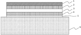
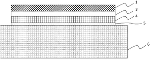
- Item 1 Includes substrate, dielectric layer, and reflective layer, The base material, the dielectric layer, and the reflective layer are laminated in this order.
- a radio wave absorber having a water vapor transmittance of 5 g / (m 2 ⁇ day) or less and a resistance value of the reflective layer after a mixed gas flow corrosion test of 100 ⁇ / ⁇ or less.
- Item 2. Item 2. The radio wave absorber according to Item 1, wherein the base material includes a support and a barrier layer, and the barrier layer is arranged between the support and the dielectric layer.
- Item 3. Item 2. The radio wave absorber according to Item 1 or 2, wherein the reflective layer has a thickness of 8 ⁇ m or more.
- Item 5. Item 2. The radio wave absorber according to any one of Items 1 to 4, wherein the absorption amount of the electromagnetic wave of 79 GHz after the mixed gas flow corrosion test is 20 dB or more.
- Item 6. Item 4. The radio wave absorber according to any one of Items 1 to 5, which is a ⁇ / 4 type radio wave absorber including a resistance film.
- Item 8. Item 6.
- Item 9. A molded product with a radio wave absorber, which comprises the radio wave absorber according to any one of Items 1 to 8.
- Item 10. A millimeter-wave radar comprising the radio wave absorber according to any one of Items 1 to 8.
- the present invention includes a base material, a dielectric layer, and a reflective layer, and the base material, the dielectric layer, and the reflective layer are laminated in this order, and the water vapor transmission rate of the base material is 5 g. / (M 2 ⁇ day) or less, and the resistance value of the reflective layer after the mixed gas flow corrosion test is 100 ⁇ / ⁇ or less (in the present specification, the “radio wave absorber of the present invention”. It may be shown as). This will be described below.
- the base material has a characteristic that the water vapor permeability is 5 g / (m 2 ⁇ day) or less. By having this property, it is possible to suppress the entry of corrosive gas into the radio wave absorber. Furthermore, the corrosive gas durability can be exhibited by combining the characteristics with the characteristics of the reflective layer described later.
- the water vapor permeability is 5 g / (m 2 ⁇ day) or less, preferably 3 g / (m 2 ⁇ day) or less, and more preferably 2 g / (m 2 ⁇ day) or less.
- the lower limit of the water vapor transmittance is not particularly limited, and is, for example, 1 ⁇ 10 ⁇ 2 g / (m 2 ⁇ day) and 1 ⁇ 10 ⁇ 1 g / (m 2 ⁇ day).
- the water vapor permeability can be measured as follows. That is, a water vapor permeation test is carried out using a moisture permeability measuring device PERMATORAN-W 3/33 (manufactured by Mocon Co., Ltd. or an equivalent product thereof). The test temperature is 40 ° C., the test humidity is 90% RH, the adhesive surface side is the detector side, and the measurement can be performed by a method according to JIS K7129: 2019.
- the base material is not particularly limited as long as it satisfies the above characteristics, but may include, for example, a support from the viewpoint of durability and the like. Further, in order to satisfy the above characteristics, the base material preferably contains a barrier layer.
- the substrate comprises a support and a barrier layer.
- the barrier layer is arranged between the support and the dielectric layer (on the surface of the support on the dielectric layer side).
- the support can increase the durability as a radio wave absorber.
- the support is not particularly limited as long as it is in the form of a sheet.
- the support is not particularly limited, and examples thereof include a resin base material.
- the resin base material is a base material containing a resin as a material, and is not particularly limited as long as it is in the form of a sheet.
- the resin base material may contain components other than the resin as long as the effects of the present invention are not significantly impaired.
- particles such as a metal oxide (for example, titanium oxide) may be contained from the viewpoint of adjusting the relative permittivity.
- the total amount of the resin in the resin base material is, for example, 80% by mass or more, preferably 90% by mass or more, more preferably 95% by mass or more, still more preferably 99% by mass or more, and usually less than 100% by mass.
- the resin is not particularly limited, and is, for example, a polyester resin such as polyethylene terephthalate (PET), polyethylene naphthalate, or modified polyester, a polyolefin such as a polyethylene (PE) resin, a polypropylene (PP) resin, a polystyrene resin, or a cyclic olefin resin.
- a polyester resin such as polyethylene terephthalate (PET), polyethylene naphthalate, or modified polyester
- a polyolefin such as a polyethylene (PE) resin, a polypropylene (PP) resin, a polystyrene resin, or a cyclic olefin resin.
- vinyl-based resins such as polyvinyl chloride and vinylidene chloride
- polyvinyl acetal resins such as polyvinyl butyral (PVB), polyether ether ketone (PEEK) resins, polysulfone (PSF) resins, polyether
- polyester resin is preferable, and polyethylene terephthalate is more preferable, from the viewpoint of productivity and strength.
- the relative permittivity of the support is not particularly limited.
- the relative permittivity of the support is, for example, 1 to 20, preferably 1 to 15, more preferably 1 to 10, and even more preferably 1 to 5.
- the relative permittivity of the support can be measured in the same manner as the relative permittivity of the dielectric layer described later.
- the thickness of the support is not particularly limited.
- the lower limit of the thickness of the support is, for example, 5 ⁇ m, preferably 10 ⁇ m, and more preferably 20 ⁇ m.
- the upper limit of the thickness of the support is, for example, 500 ⁇ m, preferably 300 ⁇ m.
- the radio wave absorber can be designed to be lightweight.
- the layer structure of the support is not particularly limited.
- the support may be composed of one type of support alone, or may be a combination of two or more types of supports.
- the barrier layer is placed on at least one surface of the support. As mentioned above, the barrier layer is preferably disposed between the support and the dielectric layer (on the surface of the support on the dielectric layer side). The barrier layer will be described in detail below. By providing the barrier layer, it becomes easy to adjust the water vapor transmittance of the radio wave absorber to 5 g / (m 2 ⁇ day) or less.
- the barrier layer is not particularly limited as long as it has a gas barrier property.
- the material of the barrier layer include metal compounds, metalloid compounds, preferably metal or metalloid oxides, nitrides, nitride oxides and the like.
- the barrier layer may contain components other than the above-mentioned materials as long as the effects of the present invention are not significantly impaired.
- the amount of the material in the barrier layer is, for example, 80% by mass or more, preferably 90% by mass or more, more preferably 95% by mass or more, still more preferably 99% by mass or more, and usually less than 100% by mass. ..
- Examples of the metal element contained in the barrier layer include titanium, aluminum, niobium, cobalt, nickel and the like.
- Examples of the metalloid element contained in the barrier layer include silicon, germanium, antimony, bismuth and the like.
- MO X As the oxide, for example, MO X [in the formula, X is a number satisfying the formula: n / 100 ⁇ X ⁇ n / 2 (n is a valence of a metal or a metalloid), and M is a metal element or It is a metalloid element. ], Examples thereof include compounds represented by.
- nitride for example in MN Y [wherein, Y has the formula: n / 100 ⁇ Y ⁇ n / 3 (n is the valence of the metal or metalloid) is a number satisfying, M is a metal element or It is a metalloid element. ], Examples thereof include compounds represented by.
- nitride oxide examples include MO X NY [in the formula, X and Y are n / 100 ⁇ X, n / 100 ⁇ Y, and X + Y ⁇ n / 2 (n is a valence of a metal or a metalloid). ), And M is a metallic element or a metalloid element. ], Examples thereof include compounds represented by.
- the oxidation number X of the oxide or oxynitride for example, the cross-section of the layer containing MOx or MOxN Y, FE-TEM-EDX (e.g., manufactured by JEOL Ltd. "JEM-ARM200F") elemental analysis by, MOx or by calculating the X elemental ratio of M and O per area of cross section of the layer containing MOxN Y, it is possible to calculate the valence of oxygen atoms.
- Y of the nitride or oxynitride for example, MN a cross-section of the layer containing the Y or MOxN Y, FE-TEM-EDX (e.g., manufactured by JEOL Ltd. "JEM-ARM200F") by elemental analysis
- the valence of nitrogen atoms can be calculated by calculating Y from the elemental ratio of M and N per area of the cross section of the layer containing, MN Y or MOxN Y.
- the material of the barrier layer include SiO 2 , SiOx, Al 2 O 3 , MgAl 2 O 4 , CuO, CuN, TiO 2 , TiN, AZO (aluminum-doped zinc oxide) and the like.
- the thickness of the barrier layer is not particularly limited.
- the lower limit of the thickness of the barrier layer is, for example, 1 nm, preferably 3 nm, and more preferably 5 nm.
- the upper limit of the thickness of the barrier layer is, for example, 100 nm, preferably 50 nm, and more preferably 30 nm.
- the thickness of the barrier layer is 100 nm or less, the wave absorption can be easily controlled.
- the layer structure of the barrier layer is not particularly limited.
- the barrier layer may be composed of one type of barrier layer alone, or may be a combination of two or more types of barrier layers.
- the dielectric layer is not particularly limited as long as it can function as a dielectric for a target wavelength in the radio wave absorber.
- the dielectric layer is not particularly limited, and examples thereof include an adhesive layer, a resin sheet, and a foam layer.
- the pressure-sensitive adhesive layer is not particularly limited as long as it contains a pressure-sensitive adhesive.
- the pressure-sensitive adhesive layer may contain components other than the pressure-sensitive adhesive as long as the effects of the present invention are not significantly impaired.
- the total amount of the resin in the resin sheet is, for example, 50% by mass or more, preferably 70% by mass or more, more preferably 90% by mass or more, still more preferably 95% by mass or more, and usually less than 100% by mass. be.
- the adhesive is not particularly limited, and is, for example, an acrylic adhesive, a urethane adhesive, a polyolefin adhesive, a polyester adhesive, a vinyl alkyl ether adhesive, a polyamide adhesive, a rubber adhesive, or a silicone adhesive.
- an acrylic adhesive is preferable from the viewpoint of high weather resistance.
- the resin sheet is not particularly limited as long as it is in the form of a sheet containing resin as a material.
- the resin sheet may contain components other than the resin as long as the effects of the present invention are not significantly impaired.
- the total amount of the resin in the resin sheet is, for example, 50% by mass or more, preferably 70% by mass or more, more preferably 90% by mass or more, still more preferably 95% by mass or more, and usually less than 100% by mass. be.
- the resin is not particularly limited, and is not particularly limited, for example, ethylene vinyl acetate copolymer (EVA), vinyl chloride, urethane, acrylic, acrylic urethane, polyolefin, polyethylene, polypropylene, silicone, polyethylene terephthalate, polyester, polystyrene, polyimide, polycarbonate, polyamide. , Polysulfone, Polyethersulphon, Synthetic resins such as epoxy, Polyisoprene rubber, Polyolefin / butadiene rubber, Polybutadiene rubber, Chloroprene rubber, Acrylonitrile / Polyolefin rubber, Butyl rubber, Acrylic rubber, Ethylene / propylene rubber, Silicone rubber, etc. It is preferable to use a rubber material as a resin component. These can be used alone or in combination of two or more.
- EVA ethylene vinyl acetate copolymer
- vinyl chloride vinyl chloride
- urethane acrylic
- acrylic urethane poly
- the dielectric layer may have adhesiveness. Therefore, when a dielectric having no adhesiveness is laminated on another layer by the pressure-sensitive adhesive layer, the combination of the dielectric and the pressure-sensitive adhesive layer is the "dielectric layer".
- the dielectric layer preferably includes a pressure-sensitive adhesive layer from the viewpoint of easy stacking with the adjacent layer.
- the relative permittivity of the dielectric layer is not particularly limited.
- the relative permittivity of the dielectric layer is, for example, 1 to 20.
- the relative permittivity is preferably 1 to 15, more preferably. Is 1 to 12, more preferably 2 to 10.
- the relative permittivity is preferably 1 to 15, more preferably 1. It is ⁇ 10, more preferably 1 ⁇ 5.
- the dielectric layer preferably contains magnetic particles. This makes it easy to adjust the relative permittivity of the dielectric layer to a suitable range.
- the magnetic particles are not particularly limited, and examples thereof include particles of metal compounds such as iron nitride, iron carbide, carbonyl iron, ferrite, magnetite, and iron ⁇ ; particles of metals such as iron, cobalt, and nickel.
- the average particle size of the magnetic particles is not particularly limited, but is preferably 0.001 to 800 ⁇ m, and more preferably 0.1 to 100 ⁇ m.
- the average particle size of the magnetic particles is the average particle size measured by a scanning electron microscope.
- the content of the magnetic particles is not particularly limited, but is, for example, 50 to 500 parts by mass, preferably 70 to 450 parts by mass, and more preferably 100 to 400 parts by mass with respect to 100 parts by mass of the resin constituting the dielectric layer. be.
- the relative permittivity of the dielectric layer can be measured by using a network analyzer, a cavity resonator, or the like, and the relative permittivity at 10 GHz can be measured by the cavity resonator permittivity method.
- the thickness of the dielectric layer is not particularly limited as long as it can exhibit radio wave absorption.
- the thickness of the dielectric layer is, for example, 100 to 2000 ⁇ m.
- the thickness is preferably 500 to 1700 ⁇ m, more preferably 800. It is ⁇ 1500 ⁇ m, more preferably 1000-1400 ⁇ m, and even more preferably 1050-1350 ⁇ m.
- the thickness is preferably 100 to 1000 ⁇ m, more preferably 200 to 800 ⁇ m. It is more preferably 300 to 700 ⁇ m, and even more preferably 350 to 650 ⁇ m.
- the thickness of the dielectric layer can be measured by Nikon DIGIMICRO STANDMS-11C + Nikon DIGIMICRO MFC-101.
- the layer structure of the dielectric layer is not particularly limited.
- the dielectric layer may be composed of one type of single dielectric layer, or may be a combination of two or more types of dielectric layers.
- a three-layer structure dielectric layer composed of a non-adhesive dielectric and adhesive layers arranged on both sides thereof, a one-layer structure dielectric layer composed of an adhesive dielectric, and the like can be mentioned.
- the reflective layer can function as a reflective layer of radio waves in a radio wave absorber.
- the reflective layer has a characteristic that the resistance value after the mixed gas flow corrosion test is 100 ⁇ / ⁇ or less.
- the corrosive gas durability can be exhibited by combining the characteristics with the characteristics of the above-mentioned base material.
- the radio wave absorber contains magnetic particles or a resistance film, the characteristics thereof and the characteristics of the above-mentioned base material can be combined to suppress the corrosion of the magnetic particles or the resistance film, and the durability of the corrosive gas is improved. do.
- the method for controlling the characteristics is not particularly limited, but for example, a method for adjusting the type of metal contained in the reflective layer, a method for adjusting the thickness of the reflective layer described later, and the water vapor transmittance of the above-mentioned substrate can be used.
- the method of adjustment and the like can be mentioned.
- the resistance value after the mixed gas flow corrosion test is preferably 50 ⁇ / ⁇ or less, more preferably 30 or less, and even more preferably 20 or less.
- the lower limit of the resistance value is not particularly limited, and is, for example, 1 ⁇ 10 -5 ⁇ / ⁇ , 1 ⁇ 10 -4 ⁇ / ⁇ .
- the mixed gas flow corrosion test can be performed as follows. The sample was allowed to stand in the test tank using a gas corrosion tester (KG120 (N), manufactured by Fact Kay, or an equivalent product thereof), and the gas concentration was adjusted based on Method 4 of IEC6000068-2-60: 2015.
- the resistance value after the mixed gas flow corrosion test can be measured as follows. That is, it can be measured by the eddy current method using a non-contact resistance measuring device (manufactured by Napson Corporation, trade name: EC-80P, or an equivalent product thereof).
- the reflective layer is not particularly limited, and examples thereof include a metal film.
- the metal film is not particularly limited as long as it is a layer containing metal as a material.
- the metal film may contain a component other than the metal as long as the effect of the present invention is not significantly impaired.
- the total amount of the metal in the metal film is, for example, 30% by mass or more, preferably 50% by mass or more, more preferably 75% by mass or more, still more preferably 80% by mass or more, still more preferably 90% by mass or more. Particularly preferably 95% by mass or more, very preferably 99% by mass or more, and usually less than 100% by mass.
- the metal is not particularly limited, and examples thereof include aluminum, copper, iron, silver, gold, nickel, chromium, molybdenum, tantalum, gallium, zinc, tin, niobium, and indium.
- nickel, chromium, molybdenum, tantalum and the like are preferable from the viewpoint of excellent stability against sulfurized gas and easy adjustment of the characteristics of the reflective layer.
- a metal compound such as ITO can also be used as a material for a metal film. These may be one kind alone or a combination of two or more kinds.
- the thickness of the reflective layer is not particularly limited.
- the thickness of the reflective layer is, for example, 1 ⁇ m or more and 1000 ⁇ m or less.
- the thickness is preferably 5 ⁇ m or more, more preferably 8 ⁇ m or more, still more preferably 10 ⁇ m or more, from the viewpoint of facilitating the adjustment of the characteristics of the reflective layer.
- the upper limit of the thickness is not particularly limited, and is, for example, 1000 ⁇ m or 500 ⁇ m.
- the layer structure of the reflective layer is not particularly limited.
- the reflective layer may be composed of one type of reflective layer alone, or may be a combination of two or more types of reflective layers.
- the radio wave absorber of the present invention can be used as either a radio wave absorber that utilizes magnetic loss or a ⁇ / 4 type radio wave absorber.
- the radio series of the present invention further includes a resistance film.
- the resistance film is not particularly limited as long as it includes a layer that can function as a resistance layer in the radio wave absorber.
- the resistance value of the resistance film is not particularly limited.
- the resistance value (sheet resistance) of the resistance film is, for example, 100 ⁇ / ⁇ or more and 800 ⁇ / ⁇ or less. Within this range, it is more preferably 150 ⁇ / ⁇ or more and 750 ⁇ / ⁇ or less, and further preferably 200 ⁇ / ⁇ or more and 600 ⁇ / ⁇ or less.
- the resistance value of the resistance film can be measured by the 4-terminal method using a surface resistance meter (manufactured by MITSUBISHI CHEMICALANALYTECH, trade name "Loresta-EP”). If the resistance film cannot be directly measured due to the lamination of dielectrics, etc., the resistance value is determined by the eddy current method using a non-contact resistance meter (product name "EC-80P, manufactured by Napson, or its equivalent). It can be measured from the surface opposite to the resistance film of the support.
- the thickness of the resistance film is not particularly limited as long as it has a resistance value that can exhibit radio wave absorption when a ⁇ / 4 type radio wave absorber is configured.
- the thickness of the resistance film is, for example, 1 nm or more and 200 nm or less, preferably 2 nm or more and 100 nm or less, and more preferably 2 nm or more and 50 nm or less.
- the layer structure of the resistance film is not particularly limited.
- the resistance film may be composed of a single layer of one type, or may be a combination of a plurality of layers of two or more types.
- the resistance value of the resistance layer is not particularly limited.
- the resistance value of the resistance layer is, for example, 100 ⁇ / ⁇ or more and 800 ⁇ / ⁇ or less. Within this range, it is more preferably 150 ⁇ / ⁇ or more and 750 ⁇ / ⁇ or less, and further preferably 200 ⁇ / ⁇ or more and 600 ⁇ / ⁇ or less.
- the thickness of the resistance layer is not particularly limited as long as it has a resistance value that can exhibit radio wave absorption when a ⁇ / 4 type radio wave absorber is configured.
- the thickness of the resistance layer is, for example, 1 nm or more and 200 nm or less, preferably 2 nm or more and 100 nm or less, and more preferably 2 nm or more and 50 nm or less.
- the layer structure of the resistance layer is not particularly limited.
- the resistance layer may be composed of one type of resistance layer alone, or may be a combination of two or more types of resistance layers.
- Indium oxide-containing resistance layer examples include a resistance layer containing a resistance layer material such as indium oxide.
- the resistance layer material preferably contains a material obtained by doping indium oxide with another material (dopant).
- dopant another material
- Other materials are not particularly limited, and examples thereof include tin oxide and zinc oxide, and mixtures thereof.
- indium oxide preferably, indium (III) oxide (In 2 O 3 ) doped with tin oxide (IV) (SnO 2 ) (indium tin oxide) (tin-).
- ITO indium oxide
- the SnO 2 content in ITO is preferably 1% by weight or more and 40% by weight because the amorphous structure is extremely stable and fluctuations in the sheet resistance of the resistance layer can be suppressed even in a high temperature and high humidity environment. Below, it is more preferably 2% by weight or more and 35% by weight or less.
- the content of the resistance layer material in the resistance layer is, for example, 50% by mass or more, preferably 70% by mass or more, more preferably 90% by mass or more, still more preferably 95% by mass or more, and usually less than 100% by mass. be.
- Molybdenum-containing resistance layer As the resistance layer, a resistance layer containing molybdenum is preferably used from the viewpoint of durability and easy adjustment of sheet resistance.
- the lower limit of the molybdenum content is not particularly limited, but from the viewpoint of further enhancing durability, 5% by weight is preferable, 7% by weight is more preferable, 9% by weight is further preferable, 11% by weight is further preferable, and 13% by weight is used. % Is particularly preferable, 15% by weight is very preferable, and 16% by weight is most preferable.
- the upper limit of the molybdenum content is preferably 30% by weight, more preferably 25% by weight, still more preferably 20% by weight, from the viewpoint of facilitating the adjustment of the surface resistance value.
- the resistance layer contains molybdenum
- nickel and chromium in addition to molybdenum in the resistance layer, a more durable radio wave absorber can be obtained.
- Alloys containing nickel, chromium and molybdenum include, for example, Hastelloy B-2, B-3, C-4, C-2000, C-22, C-276, G-30, N, W, X and the like. Various grades can be mentioned.
- the resistance layer contains molybdenum, nickel and chromium
- the molybdenum content is 5% by weight or more
- the nickel content is 40% by weight or more
- the chromium content is 1% by weight or more.
- a radio wave absorber having more excellent durability can be obtained.
- the molybdenum, nickel and chromium contents are more preferably 7% by weight or more, the nickel content is 45% by weight or more, and the chromium content is 3% by weight or more.
- the molybdenum, nickel and chromium contents are more preferably 9% by weight or more, the nickel content is 47% by weight or more, and the chromium content is 5% by weight or more.
- the molybdenum, nickel and chromium contents are more preferably 11% by weight or more, the nickel content is 50% by weight or more, and the chromium content is 10% by weight or more.
- the contents of molybdenum, nickel and chromium it is particularly preferable that the molybdenum content is 13% by weight or more, the nickel content is 53% by weight or more, and the chromium content is 12% by weight or more.
- the molybdenum content is 15% by weight or more, the nickel content is 55% by weight or more, and the chromium content is 15% by weight or more.
- the molybdenum, nickel and chromium contents are most preferably 16% by weight or more, the nickel content is 57% by weight or more, and the chromium content is 16% by weight or more.
- the nickel content is preferably 80% by weight or less, more preferably 70% by weight or less, and further preferably 65% by weight or less.
- the chromium content is preferably 50% by weight or less, more preferably 40% by weight or less, and further preferably 35% by weight or less.
- the resistance layer may contain a metal other than molybdenum, nickel and chromium.
- a metal include iron, cobalt, tungsten, manganese, titanium and the like.
- the upper limit of the total content of the metals other than molybdenum, nickel and chromium is preferably 45% by weight, more preferably 40, from the viewpoint of the durability of the resistance layer.
- weight% more preferably 35% by weight, even more preferably 30% by weight, particularly preferably 25% by weight, very preferably 23% by weight.
- the lower limit of the total content of the metals other than molybdenum, nickel and chromium is, for example, 1% by weight.
- the preferable upper limit of the content is 25% by weight, the more preferable upper limit is 20% by weight, the further preferable upper limit is 15% by weight, and the preferable lower limit is 15% by weight from the viewpoint of the durability of the resistance layer. 1% by weight.
- the preferable upper limit of the content is 5% by weight, the more preferable upper limit is 4% by weight, and the further preferable upper limit is independently from the viewpoint of the durability of the resistance layer. It is 3% by weight, and the preferable lower limit is 0.1% by weight.
- the preferable upper limit of the content is 8% by weight, the more preferable upper limit is 6% by weight, the further preferable upper limit is 4% by weight, and the preferable lower limit is 4% by weight from the viewpoint of the durability of the resistance layer. 1% by weight.
- the resistance layer may contain silicon and / or carbon.
- the content of the silicon and / or carbon is preferably 1% by weight or less, more preferably 0.5% by weight or less, respectively. ..
- the content of the silicon and / or carbon is preferably 0.01% by weight or more.
- the resistance film includes a barrier layer.
- the barrier layer is placed on at least one surface of the resistance layer. The barrier layer will be described in detail below.
- the barrier layer is not particularly limited as long as it is a layer that can protect the resistance layer and suppress its deterioration.
- the material of the barrier layer include metal compounds, metalloid compounds, preferably metal or metalloid oxides, nitrides, nitride oxides and the like.
- the barrier layer may contain components other than the above-mentioned materials as long as the effects of the present invention are not significantly impaired. In that case, the amount of the material in the barrier layer is, for example, 80% by mass or more, preferably 90% by mass or more, more preferably 95% by mass or more, still more preferably 99% by mass or more, and usually less than 100% by mass. ..
- Examples of the metal element contained in the barrier layer include titanium, aluminum, niobium, cobalt, nickel and the like.
- Examples of the metalloid element contained in the barrier layer include silicon, germanium, antimony, bismuth and the like.
- MO X As the oxide, for example, MO X [in the formula, X is a number satisfying the formula: n / 100 ⁇ X ⁇ n / 2 (n is a valence of a metal or a metalloid), and M is a metal element or It is a metalloid element. ], Examples thereof include compounds represented by.
- nitride for example in MN Y [wherein, Y has the formula: n / 100 ⁇ Y ⁇ n / 3 (n is the valence of the metal or metalloid) is a number satisfying, M is a metal element or It is a metalloid element. ], Examples thereof include compounds represented by.
- nitride oxide examples include MOXN Y [in the formula, X and Y are n / 100 ⁇ X, n / 100 ⁇ Y, and X + Y ⁇ n / 2 (n is a valence of a metal or a metalloid). ), And M is a metal element or a metalloid element. ], Examples thereof include compounds represented by.
- the oxidation number X of the oxide or oxynitride for example, the cross-section of the layer containing MOx or MOxN Y, FE-TEM-EDX (e.g., manufactured by JEOL Ltd. "JEM-ARM200F") elemental analysis by, MOx or by calculating the X elemental ratio of M and O per area of cross section of the layer containing MOxN Y, it is possible to calculate the valence of oxygen atoms.
- Y of the nitride or oxynitride for example, MN a cross-section of the layer containing the Y or MOxN Y, FE-TEM-EDX (e.g., manufactured by JEOL Ltd. "JEM-ARM200F") by elemental analysis
- the valence of nitrogen atoms can be calculated by calculating Y from the elemental ratio of M and N per area of the cross section of the layer containing, MN Y or MOxN Y.
- the material of the barrier layer include SiO 2 , SiOx, Al 2 O 3 , MgAl 2 O 4 , CuO, CuN, TiO 2 , TiN, AZO (aluminum-doped zinc oxide) and the like.
- the thickness of the barrier layer is not particularly limited.
- the thickness of the barrier layer is, for example, 1 nm or more and 200 nm or less, preferably 1 nm or more and 100 nm or less, and more preferably 1 nm or more and 20 nm or less.
- the layer structure of the barrier layer is not particularly limited.
- the barrier layer may be composed of one type of barrier layer alone, or may be a combination of two or more types of barrier layers.
- the layers are arranged in the order in which the radio wave absorption performance can be exhibited.
- the base material, the dielectric layer, and the reflective layer are arranged in this order.
- the radio wave absorber of the present invention is used as a ⁇ / 4 type radio wave absorber (that is, when a resistance film is further included)
- the base material, the resistance film, the dielectric layer, and the reflection layer are arranged in this order. ..
- a layer other than the base material, the dielectric layer, and the reflective layer (or other than the base material, the resistance film, the dielectric layer, and the reflective layer) may be included. good.
- the other layer may be placed on the surface of either the substrate, the resistance film, the dielectric layer, and the reflective layer, respectively.
- Examples of the other layer include an adhesive layer arranged on the outermost surface on the side opposite to the dielectric layer side of the reflective layer.
- This pressure-sensitive adhesive layer makes it possible to easily attach the radio wave absorber of the present invention by another member (for example, a device in an automobile). From this viewpoint, in the radio wave absorber of the present invention, it is preferable that the pressure-sensitive adhesive layer is arranged on the surface of the reflective layer opposite to the dielectric layer side.
- a barrier layer having a gas barrier property can be preferably adopted.
- a barrier layer arranged on a surface of the reflective layer opposite to the dielectric layer side can be mentioned.
- the structure of the barrier layer is the same as that of the barrier layer of the base material.
- the adhesive is not particularly limited, and is, for example, an acrylic adhesive, a urethane adhesive, a polyolefin adhesive, a polyester adhesive, a vinyl alkyl ether adhesive, a polyamide adhesive, a rubber adhesive, or a silicone adhesive. Examples thereof include adhesives and fluorine-based adhesives.
- the radio wave absorber of the present invention can preferably exhibit the performance that the absorption amount of the electromagnetic wave of 79 GHz is 20 dB or more after the mixed gas flow corrosion test.
- the absorption amount is preferably 23 dB or more, more preferably 25 dB or more.
- the upper limit of the absorption amount is not particularly limited, and is, for example, 50 dB and 60 dB.
- the performance can be measured as follows. That is, network analyzer MS4647B (manufactured by Anritsu), free space material measurement device BD1-26.
- a radio wave absorption measuring device is configured using A (manufactured by Keycom). Using this radio wave absorption measuring device, the radio wave absorption amount of the radio wave absorber at 79 GHz can be measured based on JIS R1679. Set so that the radio wave incident direction is vertical incident and the incident is from the opposite side of the reflective layer.
- the radio wave absorber of the present invention can be obtained according to or according to various methods, for example, a known manufacturing method, depending on its configuration. For example, it can be obtained by a method including a step of laminating a resistance film on a substrate, if necessary, and then laminating a dielectric layer and a reflective layer in order.
- the stacking method is not particularly limited.
- the resistance film and the barrier layer can be formed by, for example, a sputtering method, a vacuum vapor deposition method, an ion plating method, a chemical vapor deposition method, a pulse laser deposition method, or the like.
- the sputtering method is preferable from the viewpoint of film thickness controllability.
- the sputtering method is not particularly limited, and examples thereof include DC magnetron sputtering, high frequency magnetron sputtering, and ion beam sputtering.
- the sputtering apparatus may be a batch system or a roll-to-roll system.
- the dielectric layer and the reflective layer can be laminated by utilizing, for example, the adhesiveness of the dielectric layer.
- the radio wave absorber of the present invention has the ability to absorb unnecessary electromagnetic waves, it can be suitably used as a radio wave countermeasure member in, for example, an optical transceiver, a next-generation mobile communication system (5G), a short-range wireless transfer technology, and the like. Also, for other purposes, it should be used for the purpose of suppressing radio wave interference and reducing noise in the millimeter-wave radar used in intelligent transportation systems (ITS) and automobile collision prevention systems that communicate information between automobiles, roads, and people. Can be done.
- ITS intelligent transportation systems
- the present invention relates to, in one embodiment, a molded product and a molded product with a radio wave absorber, which comprises the radio wave absorber of the present invention attached to the molded product.
- the molded product include members used in the above-mentioned various uses.
- the method of attaching the radio wave absorber of the present invention to the molded product is not particularly limited, and examples thereof include a method of attaching via an adhesive and a method of attaching with a fixture.
- a millimeter-wave radar is a preferable example of a molded product with a radio wave absorber.
- the frequency of the radio wave targeted by the radio wave absorber of the present invention is preferably 10 to 150 GHz, more preferably 20 to 120 GHz, still more preferably 30 to 100 GHz, still more preferably 55 to 90 GHz, and particularly preferably 70 to 90 GHz. be.
- Example 5 A radio wave absorber utilizing magnetic loss was obtained in the same manner as in Example 1 except that the thickness of the barrier layer of the base material, the type of metal of the reflective layer, the thickness of the reflective layer, etc. were changed as described in the table below. .. (Example 5) A radio wave absorber utilizing magnetic loss was obtained in the same manner as in Example 1 except that the base material, the type of metal of the reflective layer, the thickness of the reflective layer, etc. were changed as described in the table below.
- the titanium oxide-containing PET substrate was prepared as follows.
- titanium oxide average particle size 200 nm, trade name: ST-41, manufactured by Ishihara Sangyo Co., Ltd.
- This unstretched film was stretched 3 times at 100 ° C. in the vertical direction and 3.3 times at 120 ° C. in the horizontal direction and heat-treated to obtain a PET substrate containing titanium oxide particles having a thickness of 50 ⁇ m.
- a resistance film (resistance layer / barrier layer 2) having a surface resistance value of 372 ⁇ / ⁇ was formed on the surface of the barrier layer 1 of the base material as follows. First, a resistance layer was formed by DC pulse sputtering. Sputtering was carried out using Hastelloy C-276 as a target, introduced at an output of 0.4 kW and an Ar gas flow rate of 100 sccm, and adjusted to a pressure of 0.12 Pa.
- SiO 2 is used as the barrier layer 2.
- a dielectric made of acrylic double-sided adhesive tape having a thickness of 500 ⁇ m and a relative permittivity of 2.6 was laminated on the formed resistance film, and a reflective layer made of copper having a thickness of 30 ⁇ m was further laminated on the dielectric.
- a ⁇ / 4 type radio wave absorber was obtained.
- Example 7 to 10 and Comparative Examples 4 to 6 ⁇ / 4 in the same manner as in Example 6 except that the thickness of the barrier layer of the base material, the presence or absence of the barrier layer of the base material, the type of metal of the reflective layer, the thickness of the reflective layer, etc. are changed as described in the table below. A type radio wave absorber was obtained.
- the radio wave absorber is taken out, the probe is brought into contact with the side opposite to the dielectric of the reflective layer of the radio wave absorber, and a non-contact resistance measuring instrument (manufactured by Napson Corporation, trade name: EC-80P or its equivalent) is used. It was measured by the eddy current method using the product).
- a non-contact resistance measuring instrument manufactured by Napson Corporation, trade name: EC-80P or its equivalent
- radio wave absorber Network analyzer MS4647B manufactured by Anritsu
- free space material measurement device BD1-26 A radio wave absorption measuring device was configured using A (manufactured by Keycom). Using this radio wave absorption measuring device, the radio wave absorption amount of the radio wave absorber at 79 GHz after performing the mixed gas flow corrosion test was measured based on JIS R 1679. The radio wave absorber was set so that the radio wave incident direction was vertical incident and the incident was from the direction opposite to the reflective layer.
- radio wave absorption amount When the radio wave absorption amount was 23 dB or more, it was evaluated as ⁇ , when the radio wave absorption amount was 20 dB or more and less than 23 dB, it was evaluated as ⁇ , and when it was less than 20 dB, it was evaluated as ⁇ .
Landscapes
- Physics & Mathematics (AREA)
- Electromagnetism (AREA)
- Engineering & Computer Science (AREA)
- Microelectronics & Electronic Packaging (AREA)
- Shielding Devices Or Components To Electric Or Magnetic Fields (AREA)
- Laminated Bodies (AREA)
Priority Applications (2)
| Application Number | Priority Date | Filing Date | Title |
|---|---|---|---|
| EP21817673.3A EP4161232A4 (en) | 2020-06-02 | 2021-06-02 | RADIO WAVE ABSORBERS |
| JP2021537097A JPWO2021246438A1 (https=) | 2020-06-02 | 2021-06-02 |
Applications Claiming Priority (2)
| Application Number | Priority Date | Filing Date | Title |
|---|---|---|---|
| JP2020-096038 | 2020-06-02 | ||
| JP2020096038 | 2020-06-02 |
Publications (1)
| Publication Number | Publication Date |
|---|---|
| WO2021246438A1 true WO2021246438A1 (ja) | 2021-12-09 |
Family
ID=78831113
Family Applications (1)
| Application Number | Title | Priority Date | Filing Date |
|---|---|---|---|
| PCT/JP2021/020981 Ceased WO2021246438A1 (ja) | 2020-06-02 | 2021-06-02 | 電波吸収体 |
Country Status (3)
| Country | Link |
|---|---|
| EP (1) | EP4161232A4 (https=) |
| JP (1) | JPWO2021246438A1 (https=) |
| WO (1) | WO2021246438A1 (https=) |
Families Citing this family (1)
| Publication number | Priority date | Publication date | Assignee | Title |
|---|---|---|---|---|
| WO2022235239A1 (en) * | 2021-05-04 | 2022-11-10 | Tusas- Turk Havacilik Ve Uzay Sanayii Anonim Sirketi | A radar absorbing structure |
Citations (4)
| Publication number | Priority date | Publication date | Assignee | Title |
|---|---|---|---|---|
| JP2008124154A (ja) * | 2006-11-09 | 2008-05-29 | Takiron Co Ltd | 電波吸収体 |
| JP2013236064A (ja) * | 2012-04-10 | 2013-11-21 | Idemitsu Kosan Co Ltd | ノイズ吸収積層体 |
| WO2018088492A1 (ja) * | 2016-11-10 | 2018-05-17 | マクセルホールディングス株式会社 | 電磁波吸収シート |
| JP2018098367A (ja) * | 2016-12-14 | 2018-06-21 | 日東電工株式会社 | 電磁波吸収体 |
Family Cites Families (2)
| Publication number | Priority date | Publication date | Assignee | Title |
|---|---|---|---|---|
| JP2006120836A (ja) * | 2004-10-21 | 2006-05-11 | Oji Tac Hanbai Kk | 電波吸収体用積層体および電波吸収体 |
| JP6492114B2 (ja) * | 2017-03-03 | 2019-03-27 | 日東電工株式会社 | 電磁波吸収体及び電磁波吸収体付成形品 |
-
2021
- 2021-06-02 JP JP2021537097A patent/JPWO2021246438A1/ja active Pending
- 2021-06-02 WO PCT/JP2021/020981 patent/WO2021246438A1/ja not_active Ceased
- 2021-06-02 EP EP21817673.3A patent/EP4161232A4/en not_active Withdrawn
Patent Citations (4)
| Publication number | Priority date | Publication date | Assignee | Title |
|---|---|---|---|---|
| JP2008124154A (ja) * | 2006-11-09 | 2008-05-29 | Takiron Co Ltd | 電波吸収体 |
| JP2013236064A (ja) * | 2012-04-10 | 2013-11-21 | Idemitsu Kosan Co Ltd | ノイズ吸収積層体 |
| WO2018088492A1 (ja) * | 2016-11-10 | 2018-05-17 | マクセルホールディングス株式会社 | 電磁波吸収シート |
| JP2018098367A (ja) * | 2016-12-14 | 2018-06-21 | 日東電工株式会社 | 電磁波吸収体 |
Non-Patent Citations (1)
| Title |
|---|
| See also references of EP4161232A4 * |
Also Published As
| Publication number | Publication date |
|---|---|
| JPWO2021246438A1 (https=) | 2021-12-09 |
| EP4161232A1 (en) | 2023-04-05 |
| EP4161232A4 (en) | 2024-06-26 |
Similar Documents
| Publication | Publication Date | Title |
|---|---|---|
| KR102677227B1 (ko) | λ/4 형 전파 흡수체 | |
| JP7554146B2 (ja) | 電波吸収体 | |
| WO2021246438A1 (ja) | 電波吸収体 | |
| WO2019182002A1 (ja) | λ/4型電波吸収体 | |
| JP7547209B2 (ja) | λ/4型電波吸収体 | |
| JP2021136447A (ja) | λ/4型電波吸収体 | |
| JP7587477B2 (ja) | λ/4型電波吸収体用抵抗膜部材 | |
| JP2020161584A (ja) | λ/4型電波吸収体 | |
| JP7642529B2 (ja) | λ/4型電波吸収体 | |
| JP7534997B2 (ja) | 電波吸収体 | |
| JP7502950B2 (ja) | λ/4型電波吸収体 | |
| WO2020196356A1 (ja) | λ/4型電波吸収体 | |
| WO2021060353A1 (ja) | λ/4型電波吸収体 | |
| JP7305392B2 (ja) | λ/4型電波吸収体 | |
| JP7479811B2 (ja) | λ/4型電波吸収体 | |
| JP2024095596A (ja) | 電波吸収体、電波吸収体の製造方法、電波吸収体製造用キット | |
| JP2022181199A (ja) | λ/4型電波吸収シート |
Legal Events
| Date | Code | Title | Description |
|---|---|---|---|
| ENP | Entry into the national phase |
Ref document number: 2021537097 Country of ref document: JP Kind code of ref document: A |
|
| 121 | Ep: the epo has been informed by wipo that ep was designated in this application |
Ref document number: 21817673 Country of ref document: EP Kind code of ref document: A1 |
|
| NENP | Non-entry into the national phase |
Ref country code: DE |
|
| ENP | Entry into the national phase |
Ref document number: 2021817673 Country of ref document: EP Effective date: 20230102 |
|
| WWW | Wipo information: withdrawn in national office |
Ref document number: 2021817673 Country of ref document: EP |