WO2021230292A1 - 光配線部品 - Google Patents
光配線部品 Download PDFInfo
- Publication number
- WO2021230292A1 WO2021230292A1 PCT/JP2021/018074 JP2021018074W WO2021230292A1 WO 2021230292 A1 WO2021230292 A1 WO 2021230292A1 JP 2021018074 W JP2021018074 W JP 2021018074W WO 2021230292 A1 WO2021230292 A1 WO 2021230292A1
- Authority
- WO
- WIPO (PCT)
- Prior art keywords
- optical
- face
- connectors
- wiring component
- component according
- Prior art date
Links
Images


Classifications
-
- G—PHYSICS
- G02—OPTICS
- G02B—OPTICAL ELEMENTS, SYSTEMS OR APPARATUS
- G02B6/00—Light guides; Structural details of arrangements comprising light guides and other optical elements, e.g. couplings
- G02B6/24—Coupling light guides
- G02B6/26—Optical coupling means
- G02B6/30—Optical coupling means for use between fibre and thin-film device
-
- G—PHYSICS
- G02—OPTICS
- G02B—OPTICAL ELEMENTS, SYSTEMS OR APPARATUS
- G02B6/00—Light guides; Structural details of arrangements comprising light guides and other optical elements, e.g. couplings
- G02B6/24—Coupling light guides
- G02B6/36—Mechanical coupling means
- G02B6/3608—Fibre wiring boards, i.e. where fibres are embedded or attached in a pattern on or to a substrate, e.g. flexible sheets
- G02B6/3612—Wiring methods or machines
-
- G—PHYSICS
- G02—OPTICS
- G02B—OPTICAL ELEMENTS, SYSTEMS OR APPARATUS
- G02B6/00—Light guides; Structural details of arrangements comprising light guides and other optical elements, e.g. couplings
- G02B6/24—Coupling light guides
- G02B6/26—Optical coupling means
- G02B6/27—Optical coupling means with polarisation selective and adjusting means
- G02B6/2753—Optical coupling means with polarisation selective and adjusting means characterised by their function or use, i.e. of the complete device
- G02B6/276—Removing selected polarisation component of light, i.e. polarizers
-
- G—PHYSICS
- G02—OPTICS
- G02B—OPTICAL ELEMENTS, SYSTEMS OR APPARATUS
- G02B6/00—Light guides; Structural details of arrangements comprising light guides and other optical elements, e.g. couplings
- G02B6/24—Coupling light guides
- G02B6/26—Optical coupling means
- G02B6/28—Optical coupling means having data bus means, i.e. plural waveguides interconnected and providing an inherently bidirectional system by mixing and splitting signals
- G02B6/2804—Optical coupling means having data bus means, i.e. plural waveguides interconnected and providing an inherently bidirectional system by mixing and splitting signals forming multipart couplers without wavelength selective elements, e.g. "T" couplers, star couplers
- G02B6/2808—Optical coupling means having data bus means, i.e. plural waveguides interconnected and providing an inherently bidirectional system by mixing and splitting signals forming multipart couplers without wavelength selective elements, e.g. "T" couplers, star couplers using a mixing element which evenly distributes an input signal over a number of outputs
- G02B6/2813—Optical coupling means having data bus means, i.e. plural waveguides interconnected and providing an inherently bidirectional system by mixing and splitting signals forming multipart couplers without wavelength selective elements, e.g. "T" couplers, star couplers using a mixing element which evenly distributes an input signal over a number of outputs based on multimode interference effect, i.e. self-imaging
-
- G—PHYSICS
- G02—OPTICS
- G02B—OPTICAL ELEMENTS, SYSTEMS OR APPARATUS
- G02B6/00—Light guides; Structural details of arrangements comprising light guides and other optical elements, e.g. couplings
- G02B6/24—Coupling light guides
- G02B6/26—Optical coupling means
- G02B6/28—Optical coupling means having data bus means, i.e. plural waveguides interconnected and providing an inherently bidirectional system by mixing and splitting signals
- G02B6/2804—Optical coupling means having data bus means, i.e. plural waveguides interconnected and providing an inherently bidirectional system by mixing and splitting signals forming multipart couplers without wavelength selective elements, e.g. "T" couplers, star couplers
- G02B6/2821—Optical coupling means having data bus means, i.e. plural waveguides interconnected and providing an inherently bidirectional system by mixing and splitting signals forming multipart couplers without wavelength selective elements, e.g. "T" couplers, star couplers using lateral coupling between contiguous fibres to split or combine optical signals
- G02B6/2843—Optical coupling means having data bus means, i.e. plural waveguides interconnected and providing an inherently bidirectional system by mixing and splitting signals forming multipart couplers without wavelength selective elements, e.g. "T" couplers, star couplers using lateral coupling between contiguous fibres to split or combine optical signals the couplers having polarisation maintaining or holding properties
-
- G—PHYSICS
- G02—OPTICS
- G02B—OPTICAL ELEMENTS, SYSTEMS OR APPARATUS
- G02B6/00—Light guides; Structural details of arrangements comprising light guides and other optical elements, e.g. couplings
- G02B6/24—Coupling light guides
- G02B6/36—Mechanical coupling means
- G02B6/38—Mechanical coupling means having fibre to fibre mating means
- G02B6/3807—Dismountable connectors, i.e. comprising plugs
- G02B6/3897—Connectors fixed to housings, casing, frames or circuit boards
Definitions
- Non-Patent Document 1 discloses an optical fiber array for connecting a silicon photonics chip.
- the optical fiber array of Non-Patent Document 1 bends an optical fiber that has entered the housing from one end surface of the housing, and guides the optical fiber to another end surface on a plane orthogonal to the plane including the one end surface. be.
- the optical path of the emitted light in the housing is 90 by reflecting the emitted light from the optical fiber connected to one end surface of the housing by the first or second lens provided in the housing.
- An optical connector is disclosed that collimates light whose optical path is bent by a first or second lens by a third or fourth lens.
- the optical wiring component includes a plurality of optical waveguides having a first end face and a second end face and extending from the first end face to the second end face, and the first one.
- One or more first optical connectors mounted and secured to the optical waveguide component with an adhesive at the first end face, and one or more second optical connectors mounted at the second end. To prepare for.
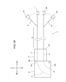
- FIG. 1A is a top view schematically showing an optical wiring component according to the first embodiment.
- FIG. 1B is a side view schematically showing the optical wiring component shown in FIG. 1A.
- FIG. 2A is a schematic view showing a first end face of the optical waveguide component in FIG. 1A.
- FIG. 2B is a schematic view showing a second end face of the optical waveguide component in FIG. 1A.
- FIG. 3 is a top view schematically showing a modified example of the optical wiring component according to the first embodiment.
- the object of the present disclosure is an optical wiring component having a bent optical waveguide, which can be miniaturized, is excellent in terms of workability and optical loss, and is unlikely to increase or break in optical loss even when the temperature changes. It is to provide optical wiring components.
- the configuration of the present disclosure is an optical wiring component having a curved optical waveguide, which can be miniaturized, is excellent in terms of workability and optical loss, and the optical loss is increased or damaged even when the temperature changes. It is possible to provide optical wiring components that are unlikely to occur.
- the optical wiring component includes a plurality of optical waveguides having a first end face and a second end face and extending from the first end face to the second end face, and the first one.
- the plurality of optical waveguides and the plurality of optical fibers are optically connected at the first end surface.
- optical wiring component having a bent optical waveguide which can be miniaturized, is excellent in terms of workability and optical loss, and is less likely to increase or break the optical loss even when the temperature changes.
- Optical wiring components can be provided. More specifically, since the above configuration bends the optical path by the optical waveguide instead of bending the optical fiber itself, it does not require a space for bending the optical fiber and can be miniaturized. In addition, since it is possible to bend the optical path only with the optical waveguide component and the optical waveguide component and the first optical connector are bonded with an adhesive, it is necessary to align a large number of optical components during work. In addition, light loss due to misalignment of optical components is unlikely to occur. Further, since the number of optical components is small, there are few places where the coefficient of thermal expansion is different, and there is a low possibility that distortion will occur when the temperature changes. As a result, the increase in light loss and damage are less likely to occur even when the temperature changes.
- the material of the optical waveguide component and the first or more optical connector may be glass containing silica as a main component.
- the "main component" in the present specification is a component having the largest composition ratio in terms of mass ratio. According to this configuration, since the optical waveguide component and the first optical connector are made of the same material, it is possible to further suppress the occurrence of distortion due to the difference in the coefficient of thermal expansion. As a result, it is possible to further suppress an increase in light loss and damage when the temperature changes.
- the material of the optical waveguide component is glass containing silica as a main component
- the first or more optical connectors may contain a ferrule made of a liquid crystal polymer.
- the difference in thermal expansion coefficient between the optical waveguide component and the first optical connector of 1 or more is preferably 5 ⁇ 10 -5 or less. According to this configuration, since the difference in the coefficient of thermal expansion between the material forming the optical waveguide component and the material forming the first optical connector is small, the occurrence of distortion due to the difference in the coefficient of thermal expansion is further increased. Can be suppressed. As a result, it is possible to further suppress an increase in light loss and damage when the temperature changes.
- the one or more first optical connectors and the one or more second optical connectors may be made of different materials. According to this configuration, it is possible to obtain a profit due to a high degree of freedom in material selection, such as manufacturing the second optical connector from a low-cost material.
- At least one of the plurality of optical fibers may be a polarization-retaining fiber. According to this configuration, it is possible to suppress polarization loss when using a laser light source.
- the number of the first optical connectors of 1 or more may be less than or equal to the number of the second optical connectors of 1 or more. According to this configuration, instead of preparing one first optical connector for one second optical connector, the number of first optical connectors to be coupled to the optical waveguide component is determined by the second optical connector. Since the number is smaller than the number, it is possible to reduce the adverse effect of variation in shape and the like caused by thermal expansion during component manufacturing.
- the plurality of optical fibers include a fiber group composed of a plurality of optical fibers having the first end face side connected in a ribbon shape, and the one or more first optical connectors include a plurality of the first optical connectors. It is a multi-core connector having a book insertion hole, and it is preferable that a plurality of optical fibers constituting the fiber group are inserted into the plurality of insertion holes. This configuration facilitates the manufacture of optical wiring components.
- the pitches of the plurality of optical waveguides may be different between the first end face and the second end face. According to this configuration, it is possible to perform optical connection at the second end face at a pitch different from that of the first end face, and for example, optical connection at the second end face at a pitch shorter than that of the first end face is also possible. can. Further, it becomes easy to match the structure of the other side to which the optical connection is made on the second end face.
- the material of the optical waveguide component preferably contains potassium, fluorine, or germanium. According to this configuration, the optical waveguide can be easily manufactured by the femtosecond laser, and the bending loss in the optical waveguide can be reduced.
- the optical wiring component preferably further contains hydrogen as a material for the optical waveguide component. According to this configuration, it is possible to efficiently aggregate potassium or germanium on the portion irradiated with the femtosecond laser, or to form a refractive index difference by irradiating the femtosecond laser. As a result, bending loss in the optical waveguide can be further reduced.
- front-back direction is the direction perpendicular to the first end face of the optical waveguide component, and the direction from the first end face toward the inside of the optical waveguide component is "front” and the direction toward the outside is “rear”. be.
- the "left-right direction” is a direction parallel to the line of intersection of the first end face and the second end face.
- the “vertical direction” is the direction perpendicular to the second end face.
- FIG. 1A is a top view schematically showing the optical wiring component 1 according to the first embodiment.
- FIG. 1B is a side view schematically showing the optical wiring component 1 shown in FIG. 1A.
- FIG. 2A is a schematic view showing a first end face 40A of the optical waveguide component 40 in FIG. 1A.
- FIG. 2B is a schematic view showing a second end face 40B of the optical waveguide component 40 in FIG. 1A.
- the optical wiring component 1 includes second optical connectors 11a to 11h and 12a to 12h, an optical fiber 21 (including 21a, 21b, 21h) and 22, a first optical connector 30, an optical waveguide component 40, and the like. It is equipped with.
- the optical wiring component 1 is for optically connecting an electronic device and another electronic device or the like.
- the optical wiring component 1 can be suitably used for applications such as optical transceivers and optical switches.
- the second optical connectors 11a to 11h (hereinafter, also referred to as the second optical connector 11) and 12a to 12h (hereinafter, also referred to as the second optical connector 12) are connectors for optical connection with an electronic device.
- the second optical connector 11 is mounted on the rear end (second end) of the optical fiber 21.
- the second optical connector 12 is mounted on the rear end (second end) of the optical fiber 22.
- the structure of the second optical connectors 11 and 12 is not particularly limited, and a conventionally known structure can be appropriately adopted as the optical connector.
- the materials of the second optical connectors 11 and 12 are not particularly limited, but are preferably resin materials such as PPS (Polyphenylene sulfide) from the viewpoint of moldability and economy.
- the number of the second optical connectors 11 and 12 is not particularly limited and may be appropriately determined according to the electronic device to be optically connected.
- the second optical connectors 11 and 12 may be one for one optical fiber or one for a plurality of optical fibers.
- the second optical connectors 11 and 12 may adopt the same configuration or different configurations, respectively. In the present embodiment, the second optical connectors 11 and 12 all have the same configuration.
- optical fibers 21 including the optical fibers 21a, 21b, and 21h are optical fibers constituting the eight-core optical fiber ribbon core wire, and are connected in a ribbon shape by the connecting portion 23. ing.
- a first optical connector 30 is mounted on the front end (first end) of the optical fiber 21.
- the portion located inside the first optical connector 30 is a glass fiber 21a', 21b', 21h', etc. (hereinafter, also referred to as a glass fiber 21') composed of only a core layer and a clad layer. be.
- a glass fiber 21' the portion from the connecting portion 23 to the second optical connector 11 is covered with an ultraviolet curable resin around the glass fiber.
- the optical fiber 22 is the same as the optical fiber 21. At least one of the optical fibers 21 and 22 may be a polarization holding fiber.
- the first optical connector 30 includes a rear end surface 30A, a front end surface 30B, and a plurality of insertion holes (not shown).
- the insertion hole extends from the rear end surface 30A to the front end surface 30B. Glass fibers 21'and 22'are inserted into the insertion holes, respectively. That is, the position of the insertion hole is the position where the glass fibers 21'and 22'exist in FIGS. 1A and 1B. A so-called V-groove may be provided instead of the insertion hole.
- the number of the first optical connectors 30 is not particularly limited, but is preferably not more than the number of the second optical connectors 11 and 12.
- the material of the first optical connector 30 is not particularly limited, but it is preferable to use a material having a difference in thermal expansion coefficient from the optical waveguide component 40 of 5 ⁇ 10 -5 or less.
- the material of the optical waveguide component 40 is preferably glass containing silica (SiO 2 ) as a main component, the first light is used from the viewpoint that the difference in the coefficient of thermal expansion from the glass satisfies the above range.
- the ferrule constituting the connector 30 is preferably made of glass containing SiO 2 as a main component or a liquid crystal polymer. Table 1 shows the preferred materials of the first optical connector 30 and the second optical connectors 11 and 12, and the coefficient of thermal expansion of the materials. As shown in Table 1, the first optical connector 30 and the second optical connectors 11 and 12 are preferably made of different materials.
- the glass fibers 21'and 22' inserted from the rear end surface 30A are fixed in a state of slightly protruding from the front end surface 30B. Then, the protruding portion is cut to form a fiber end face optically connected to the optical waveguides 41 and 42 in the first end face 40A of the optical waveguide component 40.
- the fiber end face may be subjected to a treatment such as polishing.
- the front end surface 30B and the first end surface 40A of the optical waveguide component 40 are planar.
- the front end surface 30B and the first end surface 40A are bonded by an adhesive.
- the adhesive is not particularly limited, but the difference in the coefficient of thermal expansion from the optical waveguide component 40 or the first optical connector 30 is different from the viewpoint of further increasing the optical loss and making it less likely to be damaged when the temperature changes. It is preferably 5 ⁇ 10 -5 or less. Further, since the adhesive may enter between the front end surface 30B and the first end surface 40A, it is preferable that the adhesive has a refractive index comparable to that of the core of the glass fiber 21'. Specific examples of such adhesives include optical precision adhesives.
- the optical waveguide component 40 includes a first end face 40A, a second end face 40B, and a plurality of optical waveguides 41 (including optical waveguides 41a, 41b, 41h, etc.) and 42 (including optical waveguides 42a, 42h, etc.). , Have.
- the angle ⁇ formed by the plane including the first end face 40A and the plane including the second end face 40B is 70 ° or more (in the example shown in FIG. 1B, the angle ⁇ is 90 °).
- the optical waveguides 41 and 42 extend from the first end face 40A to the second end face 40B in the optical waveguide component 40.
- Each of the optical waveguides 41 and 42 is optically connected to the fiber end face of any of the glass fibers 21'and 22'at the first end face 40A. Further, each of the optical waveguides 41 and 42 is optically connected to other electronic devices or the like on the second end surface 40B.
- the optical waveguides 41 and 42 have a high refractive index portion and a low refractive index portion that has a lower refractive index than the high refractive index portion and surrounds the high refractive index portion.
- the light incident on the optical waveguides 41 and 42 from the fiber end face travels through the high refractive index portion due to the effect of confining the light due to the difference in the refractive index between the high refractive index portion and the low refractive index portion, and exits from the second end face 40B. Will be done.
- the light incident on the optical waveguides 41 and 42 from the second end face 40B side travels through the high refractive index portion and is emitted from the first end face 40A.
- the material of the optical waveguide component 40 is preferably glass containing SiO 2 as a main component, and more preferably the glass is doped with potassium, fluorine, or germanium, in addition to the glass and the dopant. It is preferable that the glass further contains hydrogen.
- the method for forming the optical waveguides 41 and 42 is not particularly limited, but can be formed by irradiating a glass member containing SiO 2 as a main component and any of the above dopants with a femtosecond laser. Specifically, by condensing the laser light from the femtosecond laser inside the glass member, the dopant is aggregated or diffused at the condensing position, and then the condensing position is moved.
- Optical waveguides 41 and 42 having a desired path can be formed. A high refractive index portion is formed at the condensing position of the laser beam, and a low refractive index portion is formed around the condensing position. Further, by injecting hydrogen into the glass member, the difference in refractive index between the high refractive index portion and the low refractive index portion can be increased.
- the paths of the optical waveguides 41 and 42 are not particularly limited, but it is preferable that at least a part thereof is curved in the optical waveguide component 40. Further, the pitches of the optical waveguides 41 and 42 on the first end face 40A and the pitches of the optical waveguides 41 and 42 on the second end face 40B may be different. When the pitch is different, it is preferable to gradually change the pitch from the first end face 40A to the second end face 40B.
- the pitch d2 between the optical waveguides 41a and 41b in the second end face 40B is smaller than the pitch d1 between the optical waveguides 41a and 42b in the first end face 40A. It has become.
- the pitch d1 can be determined based on the diameter of the optical fiber 21 and the pitch of each optical fiber 21 in the optical fiber ribbon core wire. Further, the pitch d2 can be determined based on the structure of the electronic device on the other side to be optically connected on the second end surface 40B. As an example, the pitch d1 is 250 ⁇ m and the pitch d2 is 125 ⁇ m or less. The pitch d2 may be larger than the pitch d1.
- FIG. 3 is a top view schematically showing the optical wiring component 101 which is a modification of the optical wiring component 1.
- the optical wiring component 101 is an example in which the number of each member is changed.
- the optical wiring component 101 includes second optical connectors 111a to 111d and 112a to 112d, optical fibers 121a to 121d (hereinafter collectively referred to as “optical fiber 121"), and optical fibers 122a to 122d (hereinafter collectively referred to as “optical fiber 121"). It also includes an optical fiber (also referred to as an optical fiber 122), a first optical connector 130, and an optical waveguide component 140.
- the optical fibers 121 and 122 are 4-core optical fiber ribbon core wires. Further, the optical wiring component 101 includes two first optical connectors 130. The number of the first optical connectors 130 is smaller than the number of the second optical connectors 111a to 111d and 112a to 112d.
- the optical waveguide component 140 is formed with optical waveguides 141a to 141d corresponding to the first optical connector 130 on the right side and optical waveguides 142a to 142d corresponding to the first optical connector 130 on the left side.
- Other configurations are the same as those of the optical wiring component 1 according to the first embodiment.
Landscapes
- Physics & Mathematics (AREA)
- General Physics & Mathematics (AREA)
- Optics & Photonics (AREA)
- Optical Couplings Of Light Guides (AREA)
- Optical Integrated Circuits (AREA)
Abstract
Description
非特許文献1のように光ファイバ自体を曲げる場合、光ファイバを曲げるためのスペースが必要になるので、筐体のサイズが大きくなるという問題があった。なお、上記スペースを小さくするために、光ファイバを急激に曲げることも考えられるが、この場合、曲げ損失や破断の問題が生じてしまう。
本開示の構成によれば、曲がった光導波路を有する光配線部品であって、小型化が可能であり、作業性や光損失の面で優れ、温度変化時においても光損失の増加や破損が生じにくい光配線部品を提供することができる。
最初に本開示の実施態様を列記して説明する。本開示の一態様に係る光配線部品は、第1の端面と第2の端面とを有し、前記第1の端面から前記第2の端面まで延びる複数の光導波路を含み、前記第1の端面を含む平面と前記第2の端面を含む平面のなす角度は70°以上である光導波路部品と、第1の端と第2の端を有する複数の光ファイバと、前記第1の端に実装され、前記第1の端面で前記光導波路部品に接着剤により固定されている1以上の第1の光コネクタと、前記第2の端に実装された1以上の第2の光コネクタと、を備える。前記光配線部品において、前記複数の光導波路と前記複数の光ファイバは、前記第1の端面で光接続している。
以下、本開示に係る光配線部品の実施の形態の例を、図面を参照しつつ説明する。以下の説明では、異なる図面であっても同一又は相当の要素には同一の符号または名称を付し、重複する説明を適宜省略する。
まず、図1A及び1B、並びに図2A及び2Bを用いて、第一の実施形態に係る光配線部品について詳述をする。図1Aは、第一の実施形態に係る光配線部品1を模式的に示す上面図である。図1Bは、図1Aに示す光配線部品1を模式的に示す側面図である。図2Aは、図1A中の光導波路部品40における第1の端面40Aを示す模式図である。図2Bは、図1A中の光導波路部品40における第2の端面40Bを示す模式図である。

次に、図3を用いて、第一の実施の形態の変形例について説明する。図3は、光配線部品1の変形例である光配線部品101を模式的に示す上面図である。光配線部品101は、各部材の数等を変更した例である。
Claims (12)
- 第1の端面と第2の端面とを有し、前記第1の端面から前記第2の端面まで延びる複数の光導波路を含み、前記第1の端面を含む平面と前記第2の端面を含む平面のなす角度は70°以上である光導波路部品と、
第1の端と第2の端を有する複数の光ファイバと、
前記第1の端に実装され、前記第1の端面で前記光導波路部品に接着剤により固定されている1以上の第1の光コネクタと、
前記第2の端に実装された1以上の第2の光コネクタと、
を備える、
光配線部品。 - 前記複数の光導波路と前記複数の光ファイバは、前記第1の端面で光接続している、
請求項1に記載の光配線部品。 - 前記光導波路部品と前記1以上の第1の光コネクタの材料は、シリカを主成分としたガラスである、
請求項1または請求項2に記載の光配線部品。 - 前記光導波路部品の材料は、シリカを主成分としたガラスであり、
前記1以上の第1の光コネクタは、液晶ポリマーからなるフェルールを含む、
請求項1または請求項2に記載の光配線部品。 - 前記光導波路部品と前記1以上の第1の光コネクタの熱膨張係数差は、5×10⁻⁵以下である、
請求項1から請求項4のいずれか一項に記載の光配線部品。 - 前記1以上の第1の光コネクタと前記1以上の第2の光コネクタは異種材料である、
請求項1から請求項5のいずれか一項に記載の光配線部品。 - 前記複数の光ファイバのうち少なくとも1本は偏波保持ファイバである、
請求項1から請求項6のいずれか一項に記載の光配線部品。 - 前記1以上の第1の光コネクタの数は、前記1以上の第2の光コネクタの数以下である、
請求項1から請求項7のいずれか一項に記載の光配線部品。 - 前記複数の光ファイバは、前記第1の端面側がリボン状に連結された複数の光ファイバで構成されるファイバ群を含み、
前記1以上の第1の光コネクタは、複数本の挿通孔を有する多芯コネクタであり、
前記ファイバ群を構成する複数の光ファイバが前記複数本の挿通孔にそれぞれ挿入されている
請求項1から請求項8のいずれか一項に記載の光配線部品。 - 前記第1の端面と前記第2の端面で、前記複数の光導波路のピッチが異なる、
請求項1から請求項9のいずれか一項に記載の光配線部品。 - 前記光導波路部品の材料は、カリウム、フッ素、又はゲルマニウムを含有する、
請求項1~10いずれか一項に記載の光配線部品。 - 前記光導波路部品の材料として、さらに水素を含有する、
請求項11に記載の光配線部品。
Priority Applications (4)
| Application Number | Priority Date | Filing Date | Title |
|---|---|---|---|
| CN202180018628.2A CN115280205A (zh) | 2020-05-13 | 2021-05-12 | 光布线部件 |
| JP2022522179A JPWO2021230292A1 (ja) | 2020-05-13 | 2021-05-12 | |
| US17/909,048 US20230090783A1 (en) | 2020-05-13 | 2021-05-12 | Optical wiring component |
| GB2213200.5A GB2609764A (en) | 2020-05-13 | 2021-05-12 | Optical wiring component |
Applications Claiming Priority (2)
| Application Number | Priority Date | Filing Date | Title |
|---|---|---|---|
| JP2020084636 | 2020-05-13 | ||
| JP2020-084636 | 2020-05-13 |
Publications (1)
| Publication Number | Publication Date |
|---|---|
| WO2021230292A1 true WO2021230292A1 (ja) | 2021-11-18 |
Family
ID=78524461
Family Applications (1)
| Application Number | Title | Priority Date | Filing Date |
|---|---|---|---|
| PCT/JP2021/018074 WO2021230292A1 (ja) | 2020-05-13 | 2021-05-12 | 光配線部品 |
Country Status (5)
| Country | Link |
|---|---|
| US (1) | US20230090783A1 (ja) |
| JP (1) | JPWO2021230292A1 (ja) |
| CN (1) | CN115280205A (ja) |
| GB (1) | GB2609764A (ja) |
| WO (1) | WO2021230292A1 (ja) |
Citations (7)
| Publication number | Priority date | Publication date | Assignee | Title |
|---|---|---|---|---|
| JPH10332965A (ja) * | 1997-05-29 | 1998-12-18 | Sumitomo Electric Ind Ltd | 薄膜導波路 |
| JP2000241657A (ja) * | 1999-02-24 | 2000-09-08 | Nippon Telegr & Teleph Corp <Ntt> | 光導波路ユニット |
| JP2004191564A (ja) * | 2002-12-10 | 2004-07-08 | Mitsubishi Electric Corp | 光路変換コネクタ |
| JP2007264033A (ja) * | 2006-03-27 | 2007-10-11 | Fujitsu Ltd | 光モジュール、光伝送システム、光モジュールの製造方法 |
| JP2013238741A (ja) * | 2012-05-15 | 2013-11-28 | Nippon Telegr & Teleph Corp <Ntt> | 光モジュール |
| WO2014087974A1 (ja) * | 2012-12-05 | 2014-06-12 | 住友電気工業株式会社 | 光導波路および光ファイバ伝送系 |
| US20170146751A1 (en) * | 2015-09-22 | 2017-05-25 | Corning Optical Communications LLC | Optical interface device having a curved waveguide using laser writing and methods of forming |
Family Cites Families (2)
| Publication number | Priority date | Publication date | Assignee | Title |
|---|---|---|---|---|
| GB2395797A (en) * | 2002-11-28 | 2004-06-02 | Univ Southampton | Fabrication of optical waveguides and Bragg gratings |
| US9052475B2 (en) * | 2011-07-29 | 2015-06-09 | Hewlett-Packard Development Company, L.P. | Fiber optics connectors |
-
2021
- 2021-05-12 CN CN202180018628.2A patent/CN115280205A/zh active Pending
- 2021-05-12 US US17/909,048 patent/US20230090783A1/en not_active Abandoned
- 2021-05-12 GB GB2213200.5A patent/GB2609764A/en active Pending
- 2021-05-12 JP JP2022522179A patent/JPWO2021230292A1/ja active Pending
- 2021-05-12 WO PCT/JP2021/018074 patent/WO2021230292A1/ja active Application Filing
Patent Citations (7)
| Publication number | Priority date | Publication date | Assignee | Title |
|---|---|---|---|---|
| JPH10332965A (ja) * | 1997-05-29 | 1998-12-18 | Sumitomo Electric Ind Ltd | 薄膜導波路 |
| JP2000241657A (ja) * | 1999-02-24 | 2000-09-08 | Nippon Telegr & Teleph Corp <Ntt> | 光導波路ユニット |
| JP2004191564A (ja) * | 2002-12-10 | 2004-07-08 | Mitsubishi Electric Corp | 光路変換コネクタ |
| JP2007264033A (ja) * | 2006-03-27 | 2007-10-11 | Fujitsu Ltd | 光モジュール、光伝送システム、光モジュールの製造方法 |
| JP2013238741A (ja) * | 2012-05-15 | 2013-11-28 | Nippon Telegr & Teleph Corp <Ntt> | 光モジュール |
| WO2014087974A1 (ja) * | 2012-12-05 | 2014-06-12 | 住友電気工業株式会社 | 光導波路および光ファイバ伝送系 |
| US20170146751A1 (en) * | 2015-09-22 | 2017-05-25 | Corning Optical Communications LLC | Optical interface device having a curved waveguide using laser writing and methods of forming |
Also Published As
| Publication number | Publication date |
|---|---|
| US20230090783A1 (en) | 2023-03-23 |
| GB202213200D0 (en) | 2022-10-26 |
| CN115280205A (zh) | 2022-11-01 |
| GB2609764A (en) | 2023-02-15 |
| JPWO2021230292A1 (ja) | 2021-11-18 |
Similar Documents
| Publication | Publication Date | Title |
|---|---|---|
| US20080068719A1 (en) | Optical Element, Optical System, and Waveguide | |
| JP6520719B2 (ja) | 光接続部品 | |
| JP2020501198A (ja) | マルチチャネル光結合器アレイ | |
| JP2012194481A (ja) | 光コネクタ、光ファイバの実装方法、及び電子情報機器 | |
| JP2018040925A (ja) | 光ファイバ搭載光集積回路装置 | |
| US20170351044A1 (en) | Optical communication modules | |
| WO2017195636A1 (ja) | 光コネクタ及び光結合構造 | |
| JP2014059479A (ja) | 光コネクタの製造方法及び光コネクタ | |
| JP2007178852A (ja) | 光配線基板及びこれを用いた光モジュール | |
| WO2018135411A1 (ja) | 光導波路部材及び光結合構造 | |
| CN114600019B (zh) | 光纤连接部件以及光纤连接结构 | |
| WO2021230292A1 (ja) | 光配線部品 | |
| JP2010066474A (ja) | 光学接続構造 | |
| WO2018181782A1 (ja) | 光レセプタクル及び光トランシーバ | |
| JP5547686B2 (ja) | マルチコアファイバ用ファンナウト部品 | |
| JP2001324647A (ja) | 光ファイバアレイ、光導波路チップ及びこれらを接続した光モジュール | |
| WO2020091015A1 (ja) | 光学接続部品 | |
| US11372164B2 (en) | Optical connector system and optical connection structure | |
| WO2020027125A1 (ja) | 光接続部品 | |
| JP6810076B2 (ja) | ファイバモジュール | |
| JP2016212414A (ja) | 導波路用結合回路 | |
| JP5059715B2 (ja) | 光学接続構造 | |
| JP2006154868A (ja) | レンズ機能付き光ファイバおよびその製造方法 | |
| JP2018146894A (ja) | 光コネクタ | |
| US20230176286A1 (en) | Optical components and optical connectors having a splice-on connection and method of fabricating the same |
Legal Events
| Date | Code | Title | Description |
|---|---|---|---|
| 121 | Ep: the epo has been informed by wipo that ep was designated in this application |
Ref document number: 21805157 Country of ref document: EP Kind code of ref document: A1 |
|
| ENP | Entry into the national phase |
Ref document number: 202213200 Country of ref document: GB Kind code of ref document: A Free format text: PCT FILING DATE = 20210512 |
|
| ENP | Entry into the national phase |
Ref document number: 2022522179 Country of ref document: JP Kind code of ref document: A |
|
| NENP | Non-entry into the national phase |
Ref country code: DE |
|
| 122 | Ep: pct application non-entry in european phase |
Ref document number: 21805157 Country of ref document: EP Kind code of ref document: A1 |