WO2021221119A1 - 配線基板及び配線基板の製造方法 - Google Patents
配線基板及び配線基板の製造方法 Download PDFInfo
- Publication number
- WO2021221119A1 WO2021221119A1 PCT/JP2021/017032 JP2021017032W WO2021221119A1 WO 2021221119 A1 WO2021221119 A1 WO 2021221119A1 JP 2021017032 W JP2021017032 W JP 2021017032W WO 2021221119 A1 WO2021221119 A1 WO 2021221119A1
- Authority
- WO
- WIPO (PCT)
- Prior art keywords
- wiring
- wiring board
- less
- substrate
- mesh
- Prior art date
- Legal status (The legal status is an assumption and is not a legal conclusion. Google has not performed a legal analysis and makes no representation as to the accuracy of the status listed.)
- Ceased
Links
Images










Classifications
-
- H—ELECTRICITY
- H01—ELECTRIC ELEMENTS
- H01Q—ANTENNAS, i.e. RADIO AERIALS
- H01Q1/00—Details of, or arrangements associated with, antennas
- H01Q1/36—Structural form of radiating elements, e.g. cone, spiral, umbrella; Particular materials used therewith
- H01Q1/38—Structural form of radiating elements, e.g. cone, spiral, umbrella; Particular materials used therewith formed by a conductive layer on an insulating support
-
- H—ELECTRICITY
- H05—ELECTRIC TECHNIQUES NOT OTHERWISE PROVIDED FOR
- H05K—PRINTED CIRCUITS; CASINGS OR CONSTRUCTIONAL DETAILS OF ELECTRIC APPARATUS; MANUFACTURE OF ASSEMBLAGES OF ELECTRICAL COMPONENTS
- H05K1/00—Printed circuits
- H05K1/18—Printed circuits structurally associated with non-printed electric components
- H05K1/181—Printed circuits structurally associated with non-printed electric components associated with surface mounted components
-
- H—ELECTRICITY
- H01—ELECTRIC ELEMENTS
- H01Q—ANTENNAS, i.e. RADIO AERIALS
- H01Q1/00—Details of, or arrangements associated with, antennas
- H01Q1/36—Structural form of radiating elements, e.g. cone, spiral, umbrella; Particular materials used therewith
-
- H—ELECTRICITY
- H01—ELECTRIC ELEMENTS
- H01Q—ANTENNAS, i.e. RADIO AERIALS
- H01Q1/00—Details of, or arrangements associated with, antennas
- H01Q1/36—Structural form of radiating elements, e.g. cone, spiral, umbrella; Particular materials used therewith
- H01Q1/364—Structural form of radiating elements, e.g. cone, spiral, umbrella; Particular materials used therewith using a particular conducting material, e.g. superconductor
-
- H—ELECTRICITY
- H01—ELECTRIC ELEMENTS
- H01Q—ANTENNAS, i.e. RADIO AERIALS
- H01Q5/00—Arrangements for simultaneous operation of antennas on two or more different wavebands, e.g. dual-band or multi-band arrangements
- H01Q5/20—Arrangements for simultaneous operation of antennas on two or more different wavebands, e.g. dual-band or multi-band arrangements characterised by the operating wavebands
- H01Q5/22—RF wavebands combined with non-RF wavebands, e.g. infrared or optical
-
- H—ELECTRICITY
- H05—ELECTRIC TECHNIQUES NOT OTHERWISE PROVIDED FOR
- H05K—PRINTED CIRCUITS; CASINGS OR CONSTRUCTIONAL DETAILS OF ELECTRIC APPARATUS; MANUFACTURE OF ASSEMBLAGES OF ELECTRICAL COMPONENTS
- H05K1/00—Printed circuits
- H05K1/02—Details
- H05K1/0274—Optical details, e.g. printed circuits comprising integral optical means
-
- H—ELECTRICITY
- H05—ELECTRIC TECHNIQUES NOT OTHERWISE PROVIDED FOR
- H05K—PRINTED CIRCUITS; CASINGS OR CONSTRUCTIONAL DETAILS OF ELECTRIC APPARATUS; MANUFACTURE OF ASSEMBLAGES OF ELECTRICAL COMPONENTS
- H05K1/00—Printed circuits
- H05K1/02—Details
- H05K1/03—Use of materials for the substrate
- H05K1/0313—Organic insulating material
-
- H—ELECTRICITY
- H05—ELECTRIC TECHNIQUES NOT OTHERWISE PROVIDED FOR
- H05K—PRINTED CIRCUITS; CASINGS OR CONSTRUCTIONAL DETAILS OF ELECTRIC APPARATUS; MANUFACTURE OF ASSEMBLAGES OF ELECTRICAL COMPONENTS
- H05K1/00—Printed circuits
- H05K1/02—Details
- H05K1/09—Use of materials for the conductive, e.g. metallic pattern
-
- H—ELECTRICITY
- H05—ELECTRIC TECHNIQUES NOT OTHERWISE PROVIDED FOR
- H05K—PRINTED CIRCUITS; CASINGS OR CONSTRUCTIONAL DETAILS OF ELECTRIC APPARATUS; MANUFACTURE OF ASSEMBLAGES OF ELECTRICAL COMPONENTS
- H05K3/00—Apparatus or processes for manufacturing printed circuits
- H05K3/10—Apparatus or processes for manufacturing printed circuits in which conductive material is applied to the insulating support in such a manner as to form the desired conductive pattern
- H05K3/108—Apparatus or processes for manufacturing printed circuits in which conductive material is applied to the insulating support in such a manner as to form the desired conductive pattern by semi-additive methods; masks therefor
-
- H—ELECTRICITY
- H05—ELECTRIC TECHNIQUES NOT OTHERWISE PROVIDED FOR
- H05K—PRINTED CIRCUITS; CASINGS OR CONSTRUCTIONAL DETAILS OF ELECTRIC APPARATUS; MANUFACTURE OF ASSEMBLAGES OF ELECTRICAL COMPONENTS
- H05K3/00—Apparatus or processes for manufacturing printed circuits
- H05K3/30—Assembling printed circuits with electric components, e.g. with resistors
- H05K3/303—Assembling printed circuits with electric components, e.g. with resistors with surface mounted components
-
- H—ELECTRICITY
- H05—ELECTRIC TECHNIQUES NOT OTHERWISE PROVIDED FOR
- H05K—PRINTED CIRCUITS; CASINGS OR CONSTRUCTIONAL DETAILS OF ELECTRIC APPARATUS; MANUFACTURE OF ASSEMBLAGES OF ELECTRICAL COMPONENTS
- H05K2201/00—Indexing scheme relating to printed circuits covered by H05K1/00
- H05K2201/01—Dielectrics
- H05K2201/0104—Properties and characteristics in general
- H05K2201/0108—Transparent
-
- H—ELECTRICITY
- H05—ELECTRIC TECHNIQUES NOT OTHERWISE PROVIDED FOR
- H05K—PRINTED CIRCUITS; CASINGS OR CONSTRUCTIONAL DETAILS OF ELECTRIC APPARATUS; MANUFACTURE OF ASSEMBLAGES OF ELECTRICAL COMPONENTS
- H05K2201/00—Indexing scheme relating to printed circuits covered by H05K1/00
- H05K2201/01—Dielectrics
- H05K2201/0137—Materials
- H05K2201/0158—Polyalkene or polyolefin, e.g. polyethylene [PE], polypropylene [PP]
-
- H—ELECTRICITY
- H05—ELECTRIC TECHNIQUES NOT OTHERWISE PROVIDED FOR
- H05K—PRINTED CIRCUITS; CASINGS OR CONSTRUCTIONAL DETAILS OF ELECTRIC APPARATUS; MANUFACTURE OF ASSEMBLAGES OF ELECTRICAL COMPONENTS
- H05K2201/00—Indexing scheme relating to printed circuits covered by H05K1/00
- H05K2201/03—Conductive materials
- H05K2201/0332—Structure of the conductor
- H05K2201/0335—Layered conductors or foils
- H05K2201/0347—Overplating, e.g. for reinforcing conductors or bumps; Plating over filled vias
-
- H—ELECTRICITY
- H05—ELECTRIC TECHNIQUES NOT OTHERWISE PROVIDED FOR
- H05K—PRINTED CIRCUITS; CASINGS OR CONSTRUCTIONAL DETAILS OF ELECTRIC APPARATUS; MANUFACTURE OF ASSEMBLAGES OF ELECTRICAL COMPONENTS
- H05K2201/00—Indexing scheme relating to printed circuits covered by H05K1/00
- H05K2201/09—Shape and layout
- H05K2201/09209—Shape and layout details of conductors
- H05K2201/09654—Shape and layout details of conductors covering at least two types of conductors provided for in H05K2201/09218 - H05K2201/095
- H05K2201/09681—Mesh conductors, e.g. as a ground plane
-
- H—ELECTRICITY
- H05—ELECTRIC TECHNIQUES NOT OTHERWISE PROVIDED FOR
- H05K—PRINTED CIRCUITS; CASINGS OR CONSTRUCTIONAL DETAILS OF ELECTRIC APPARATUS; MANUFACTURE OF ASSEMBLAGES OF ELECTRICAL COMPONENTS
- H05K2201/00—Indexing scheme relating to printed circuits covered by H05K1/00
- H05K2201/10—Details of components or other objects attached to or integrated in a printed circuit board
- H05K2201/10007—Types of components
- H05K2201/10098—Components for radio transmission, e.g. radio frequency identification [RFID] tag, printed or non-printed antennas
-
- H—ELECTRICITY
- H05—ELECTRIC TECHNIQUES NOT OTHERWISE PROVIDED FOR
- H05K—PRINTED CIRCUITS; CASINGS OR CONSTRUCTIONAL DETAILS OF ELECTRIC APPARATUS; MANUFACTURE OF ASSEMBLAGES OF ELECTRICAL COMPONENTS
- H05K2203/00—Indexing scheme relating to apparatus or processes for manufacturing printed circuits covered by H05K3/00
- H05K2203/03—Metal processing
- H05K2203/0307—Providing micro- or nanometer scale roughness on a metal surface, e.g. by plating of nodules or dendrites
-
- H—ELECTRICITY
- H05—ELECTRIC TECHNIQUES NOT OTHERWISE PROVIDED FOR
- H05K—PRINTED CIRCUITS; CASINGS OR CONSTRUCTIONAL DETAILS OF ELECTRIC APPARATUS; MANUFACTURE OF ASSEMBLAGES OF ELECTRICAL COMPONENTS
- H05K3/00—Apparatus or processes for manufacturing printed circuits
- H05K3/10—Apparatus or processes for manufacturing printed circuits in which conductive material is applied to the insulating support in such a manner as to form the desired conductive pattern
- H05K3/18—Apparatus or processes for manufacturing printed circuits in which conductive material is applied to the insulating support in such a manner as to form the desired conductive pattern using precipitation techniques to apply the conductive material
- H05K3/188—Apparatus or processes for manufacturing printed circuits in which conductive material is applied to the insulating support in such a manner as to form the desired conductive pattern using precipitation techniques to apply the conductive material by direct electroplating
-
- H—ELECTRICITY
- H05—ELECTRIC TECHNIQUES NOT OTHERWISE PROVIDED FOR
- H05K—PRINTED CIRCUITS; CASINGS OR CONSTRUCTIONAL DETAILS OF ELECTRIC APPARATUS; MANUFACTURE OF ASSEMBLAGES OF ELECTRICAL COMPONENTS
- H05K3/00—Apparatus or processes for manufacturing printed circuits
- H05K3/38—Improvement of the adhesion between the insulating substrate and the metal
- H05K3/386—Improvement of the adhesion between the insulating substrate and the metal by the use of an organic polymeric bonding layer, e.g. adhesive
-
- H—ELECTRICITY
- H05—ELECTRIC TECHNIQUES NOT OTHERWISE PROVIDED FOR
- H05K—PRINTED CIRCUITS; CASINGS OR CONSTRUCTIONAL DETAILS OF ELECTRIC APPARATUS; MANUFACTURE OF ASSEMBLAGES OF ELECTRICAL COMPONENTS
- H05K3/00—Apparatus or processes for manufacturing printed circuits
- H05K3/38—Improvement of the adhesion between the insulating substrate and the metal
- H05K3/388—Improvement of the adhesion between the insulating substrate and the metal by the use of a metallic or inorganic thin film adhesion layer
Definitions
- the embodiment of the present disclosure relates to a wiring board and a method of manufacturing the wiring board.
- mobile terminal devices such as smartphones and tablets are becoming more sophisticated, smaller, thinner and lighter. Since these mobile terminal devices use a plurality of communication bands, a plurality of antennas corresponding to the communication bands are required.
- mobile terminal devices include telephone antennas, WiFi (Wireless Fidelity) antennas, 3G (Generation) antennas, 4G (Generation) antennas, LTE (Long Term Evolution) antennas, and Bluetooth (registered trademark) antennas.
- NFC Near Field Communication
- This film antenna is a transparent antenna in which an antenna pattern is formed on a transparent base material, and the antenna pattern is a mesh composed of a conductor portion as a forming portion of an opaque conductor layer and a large number of openings as a non-forming portion. It is formed by a conductive mesh layer in the shape of a shape.
- a mesh wiring layer (conductor mesh layer) is mounted on a transparent base material.
- high-frequency electromagnetic waves have been used in film antennas.
- the number of times electrons pass through the grain boundaries of the metal constituting the mesh wiring layer per unit time increases, so that current does not easily flow and transmission loss may increase.
- the present embodiment provides a wiring board and a method for manufacturing a wiring board, which can suppress the difficulty of current flowing through the mesh wiring layer.
- the wiring board according to the present embodiment is a wiring board, which includes a board and a mesh wiring layer arranged on the board and including a plurality of wirings, and the board has a wavelength of 400 nm or more and 700 nm or less.
- the transmittance is 85% or more
- the wiring includes a surface roughness Ra
- the surface roughness Ra is 100 nm or less.
- the wiring may include a metal crystal, and the area average particle diameter of the metal crystal may be 300 nm or more.
- the line width of the wiring may be 0.1 ⁇ m or more and 5.0 ⁇ m or less.
- the mesh wiring layer may be an antenna.
- the wiring may include gold, silver, copper, platinum, tin, aluminum, iron or nickel.
- the dielectric loss tangent of the board may be 0.002 or less.
- the thickness of the board may be 5 ⁇ m or more and 200 ⁇ m or less.
- the board may contain a cycloolefin polymer or a polynorbornene polymer.
- the mesh wiring layer may exist only in a part of the board.
- the surface roughness Ra may be 90 nm or less.
- the method for manufacturing a wiring board according to the present embodiment is a method for manufacturing a wiring board, which includes a step of preparing a board and a step of forming a mesh wiring layer including a plurality of wires on the board.
- the substrate has a light transmittance of 85% or more and a wavelength of 400 nm or more and 700 nm or less, the wiring includes a surface roughness Ra, and the surface roughness Ra is 100 nm or less.
- the wiring may include a metal crystal, and the area average particle diameter of the metal crystal may be 300 nm or more.
- the line width of the wiring may be 0.1 ⁇ m or more and 5.0 ⁇ m or less.
- the mesh wiring layer may be an antenna.
- the wiring may include gold, silver, copper, platinum, tin, aluminum, iron or nickel.
- the dielectric loss tangent of the board may be 0.002 or less.
- the thickness of the board may be 5 ⁇ m or more and 200 ⁇ m or less.
- the board may contain a cycloolefin polymer or a polynorbornene polymer.
- the mesh wiring layer may exist only in a part of the board.
- the surface roughness Ra may be 90 nm or less.
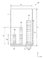
- FIG. 1 is a plan view showing a wiring board according to an embodiment.
- FIG. 2 is an enlarged plan view showing a wiring board according to one embodiment (enlarged view of part II of FIG. 1).
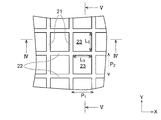
- FIG. 3 is an enlarged plan view showing a wiring board according to one embodiment (enlarged view of part III of FIG. 2).
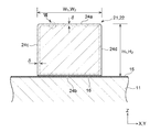
- FIG. 4 is a cross-sectional view showing a wiring board according to one embodiment (VI-VI line cross-sectional view of FIG. 3).
- FIG. 5 is a cross-sectional view (VV line cross-sectional view of FIG. 3) showing a wiring board according to one embodiment.
- FIG. 6 is a cross-sectional view showing the first-direction wiring and the second-direction wiring.
- FIG. 7 is an enlarged cross-sectional view showing a part of the first-direction wiring and the second-direction wiring (enlarged view of part VII in FIG. 6).
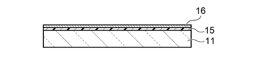
- 8A-8E are cross-sectional views showing a method of manufacturing a wiring board according to an embodiment.
- 9A-9E are cross-sectional views showing a method of manufacturing a wiring board according to an embodiment.
- FIG. 10 is a plan view showing an image display device according to an embodiment.
- FIG. 11 is a plan view showing a wiring board according to Example 1-2 and Comparative Example 1.
- FIGS. 1 to 10 are diagrams showing the present embodiment.
- the "X direction” is a direction parallel to one side of the substrate.
- the "Y direction” is a direction perpendicular to the X direction and parallel to the other side of the substrate.
- the “Z direction” is a direction perpendicular to both the X direction and the Y direction and parallel to the thickness direction of the wiring board.
- the "surface” is a surface on the plus side in the Z direction, and refers to a surface on which wiring is provided with respect to the substrate.
- the “back surface” refers to a surface on the minus side in the Z direction, which is opposite to the surface on which wiring is provided with respect to the substrate.
- FIGS. 1 to 7 are diagrams showing a wiring board according to the present embodiment.
- the wiring board 10 is arranged, for example, on the display of an image display device.
- a wiring board 10 includes a transparent board 11 and a mesh wiring layer (wiring pattern area) 20 arranged on the board 11. Further, the power feeding unit 40 is electrically connected to the mesh wiring layer 20.
- the substrate 11 has a substantially rectangular shape in a plan view, its longitudinal direction is parallel to the Y direction, and its lateral direction is parallel to the X direction.
- the substrate 11 is transparent and has a substantially flat plate shape, and the thickness thereof is substantially uniform as a whole.
- the length L 1 in the longitudinal direction (Y direction) of the substrate 11 can be selected, for example, in the range of 2 mm or more and 300 mm or less, and preferably in the range of 100 mm or more and 200 mm or less.
- the length L 2 in the lateral direction (X direction) of the substrate 11 can be selected in the range of 2 mm or more and 300 mm or less, and preferably, for example, 50 mm or more and 100 mm or less.
- the corners of the substrate 11 may be rounded.
- the material of the substrate 11 may be any material having transparency and electrical insulation in the visible light region.
- the material of the substrate 11 is polyethylene terephthalate, but the material is not limited to this.
- the material of the substrate 11 include polyester resins such as polyethylene terephthalate, acrylic resins such as pomethylmethacrylate, polycarbonate resins, polyimide resins, polyolefin resins such as cycloolefin polymers, and triacetyl cellulose. It is preferable to use an organic insulating material such as the cellulose-based resin material of.
- an organic insulating material such as a cycloolefin polymer (for example, ZF-16 manufactured by ZEON Corporation) or a polynorbornene polymer (manufactured by Sumitomo Bakelite Co., Ltd.) may be used.
- a cycloolefin polymer for example, ZF-16 manufactured by ZEON Corporation
- a polynorbornene polymer manufactured by Sumitomo Bakelite Co., Ltd.
- glass, ceramics and the like can be appropriately selected depending on the intended use.
- the substrate 11 is not limited to this, and may have a structure in which a plurality of base materials or layers are laminated. Further, the substrate 11 may be in the form of a film or a plate.
- the thickness of the substrate 11 is not particularly limited and can be appropriately selected depending on the application.
- the thickness (Z direction) T 1 (see FIGS. 4 and 5) of the substrate 11 is, for example, 5 ⁇ m or more and 200 ⁇ m. It can be in the following range.
- the dielectric loss tangent of the substrate 11 may be 0.002 or less, preferably 0.001 or less.
- the lower limit of the dielectric loss tangent of the substrate 11 is not particularly limited, but it may be more than 0.
- the lower limit of the dielectric loss tangent of the substrate 11 is not particularly limited.
- the dielectric constant of the substrate 11 is not particularly limited, but may be 2.0 or more and 10.0 or less.
- the dielectric loss tangent of the substrate 11 can be measured in accordance with IEC 62562. Specifically, first, the substrate 11 in the portion where the mesh wiring layer 20 is not formed is cut out to prepare a test piece. Alternatively, the substrate 11 on which the mesh wiring layer 20 is formed may be cut out and the mesh wiring layer 20 may be removed by etching or the like. The dimensions of the test piece are 10 mm to 20 mm in width and 50 mm to 100 mm in length. Next, the dielectric loss tangent is measured according to IEC 62562. The dielectric constant and the dielectric loss tangent of the substrate 11 can also be measured according to ASTM D150.
- the substrate 11 may have a transmittance of visible light (light rays having a wavelength of 400 nm or more and 700 nm or less) of 85% or more, preferably 90% or more.
- the upper limit of the visible light transmittance of the substrate 11 is not particularly limited, but may be 100% or less, for example.
- the visible light means a light having a wavelength of 400 nm to 700 nm.
- the absorbance of the substrate 11 is measured using a known spectrophotometer (for example, a spectroscope manufactured by JASCO Corporation: V-670). At that time, it means that the transmittance is 85% or more in the entire wavelength region of 400 nm to 700 nm.
- a known spectrophotometer for example, a spectroscope manufactured by JASCO Corporation: V-670. At that time, it means that the transmittance is 85% or more in the entire wavelength region of 400 nm to 700 nm.
- the mesh wiring layer 20 is composed of an antenna pattern region having a function as an antenna.
- a plurality (three) of mesh wiring layers 20 are formed on the substrate 11, and each corresponds to a different frequency band. That is, the plurality of mesh interconnect layer 20, its length is different (Y length direction) L a mutually have a length corresponding to the respective specific frequency bands. Incidentally, the corresponding frequency band length L a certain extent the mesh wiring layer 20 at a low frequency is longer.
- each mesh wiring layer 20 has a telephone antenna, a WiFi antenna, a 3G antenna, a 4G antenna, and 5G.
- the mesh wiring layer 20 may not exist on the entire surface of the substrate 11, but may exist only in a partial region on the substrate 11.
- Each mesh wiring layer 20 has a substantially rectangular shape in a plan view.
- the longitudinal direction of each mesh wiring layer 20 is parallel to the Y direction, and the lateral direction thereof is parallel to the X direction.
- the length L a of the longitudinal direction of each mesh wiring layers 20 (Y direction) can be selected by 100mm below the range of 3 mm
- the width W a of the transverse direction of the mesh interconnect layer 20 (X-direction) Can be selected, for example, in the range of 1 mm or more and 10 mm or less.
- the mesh wiring layer 20 may be a millimeter wave antenna. If the mesh wiring layer 20 is an antenna for millimeter waves, the length L a of the mesh wiring layer 20, 1 mm or more 10mm or less, more preferably be selected in 5mm below the range of 1.5 mm.
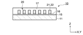
- the mesh wiring layer 20 has metal wires formed in a grid shape or a mesh shape, respectively, and has a repeating pattern in the X direction and the Y direction. That is, the mesh wiring layer 20 has a pattern shape composed of a portion extending in the X direction (second direction wiring 22) and a portion extending in the Y direction (first direction wiring 21).
- each mesh wiring layer 20 has a plurality of first-direction wirings (antenna wirings) 21 having a function as an antenna, and a plurality of second-direction wirings (a plurality of second-direction wirings (21) connecting the plurality of first-direction wirings 21.
- Antenna connection wiring) 22 is included.
- the plurality of first-direction wirings 21 and the plurality of second-direction wirings 22 are integrated as a whole to form a grid shape or a mesh shape.
- Each first-direction wiring 21 extends in a direction corresponding to the frequency band of the antenna (longitudinal direction, Y direction), and each second-direction wiring 22 extends in a direction orthogonal to the first-direction wiring 21 (width direction, X). Extends in the direction).
- the second direction wiring 22 by connecting these first direction wirings 21 to each other, the first direction wiring 21 is disconnected or the first direction wiring 21 and the power feeding unit 40 are not electrically connected. It plays a role in suppressing problems such as wiring.
- each mesh wiring layer 20 a plurality of openings 23 are formed by being surrounded by a first-direction wiring 21 adjacent to each other and a second-direction wiring 22 adjacent to each other. .. Further, the first-direction wiring 21 and the second-direction wiring 22 are arranged at equal intervals with each other. That is, the plurality of first-direction wirings 21 are arranged at equal intervals with each other, and the pitch P 1 thereof can be, for example, in the range of 0.01 mm or more and 1 mm or less. Further, the plurality of second-direction wirings 22 are arranged at equal intervals with each other, and the pitch P 2 thereof can be, for example, in the range of 0.01 mm or more and 1 mm or less.
- each opening 23 has a substantially square shape in a plan view, and the transparent substrate 11 is exposed from each opening 23. Therefore, by increasing the area of each opening 23, the transparency of the wiring board 10 as a whole can be improved.
- the length L 3 of one side of each opening 23 can be, for example, in the range of 0.01 mm or more and 1 mm or less.
- the first-direction wiring 21 and the second-direction wiring 22 are orthogonal to each other, but are not limited to this, and may intersect each other at an acute angle or an obtuse angle. Further, the shape of the opening 23 is preferably the same shape and the same size on the entire surface, but it does not have to be uniform on the entire surface such as changing depending on the location.
- each first-direction wiring 21 has a substantially rectangular shape or a substantially square shape in a cross section perpendicular to the longitudinal direction (cross section in the X direction).
- the cross-sectional shape of the first-direction wiring 21 is substantially uniform along the longitudinal direction (Y direction) of the first-direction wiring 21.
- the shape of the cross section (Y direction cross section) perpendicular to the longitudinal direction of each second direction wiring 22 is a substantially rectangular shape or a substantially square shape, and the cross section of the first direction wiring 21 described above. (Cross section in X direction) It is almost the same as the shape.
- the cross-sectional shape of the second direction wiring 22 is substantially uniform along the longitudinal direction (X direction) of the second direction wiring 22.
- the cross-sectional shape of the first-direction wiring 21 and the second-direction wiring 22 does not necessarily have to be a substantially rectangular shape or a substantially square shape.
- the cross-sectional shape of the first-direction wiring 21 and the second-direction wiring 22 is, for example, a substantially trapezoidal shape in which the front surface side (plus side in the Z direction) is narrower than the back surface side (minus side in the Z direction), or side surfaces located on both sides in the longitudinal direction. May have a curved shape.
- the line width W 1 of the first direction wiring 21 (length in the X direction, see FIG. 4) and the line width W 2 of the second direction wiring 22 (length in the Y direction, see FIG. 5) are , Is not particularly limited, and can be appropriately selected according to the intended use.
- the line width W 1 of the first direction wiring 21 can be selected in the range of 0.1 ⁇ m or more and 5.0 ⁇ m or less, and is preferably 0.2 ⁇ m or more and 2.0 ⁇ m or less.
- the line width W 2 of the second direction wiring 22 can be selected in the range of 0.1 ⁇ m or more and 5.0 ⁇ m or less, and is preferably 0.2 ⁇ m or more and 2.0 ⁇ m or less.
- the height H 1 of the first direction wiring 21 (length in the Z direction, see FIG. 4) and the height H 2 of the second direction wiring 22 (length in the Z direction, see FIG. 5) are not particularly limited. It can be appropriately selected depending on the intended use, for example, it can be selected in the range of 0.1 ⁇ m or more and 5.0 ⁇ m or less, and preferably 0.2 ⁇ m or more and 2.0 ⁇ m or less.
- FIG. 6 shows a cross section of the first direction wiring 21 and the second direction wiring 22 in the width direction (X direction, Y direction).
- the first-direction wiring 21 and the second-direction wiring 22 have a front surface 24a, a back surface 24b, and two side surfaces 24c and 24d, respectively.
- the surface 24a is located on the side where the first-direction wiring 21 and the second-direction wiring 22 are visible to the observer (plus side in the Z direction) during use.
- the back surface 24b is located on the opposite side of the front surface 24a and on the substrate 11 side (minus side in the Z direction).
- the two side surfaces 24c and 24d are located between the front surface 24a and the back surface 24b, and are located on both sides of the first direction wiring 21 and the second direction wiring 22 in the width direction (X direction and Y direction), respectively.
- the front surface 24a and the side surfaces 24c and 24d are substantially orthogonal to each other
- the back surface 24b and the side surfaces 24c and 24d are substantially orthogonal to each other, but the present invention is not limited to this and may intersect at an acute angle or an obtuse angle.
- front surface 24a, the back surface 24b and the side surfaces 24c and 24d are respectively extended linearly, but the present invention is not limited to this, and the front surface 24a, the back surface 24b or the side surfaces 24c and 24d may be curved, respectively.
- FIG. 7 is an enlarged schematic view showing the vicinity of the surface 24a of the first direction wiring 21 and the second direction wiring 22. As shown in FIG. 7, the size of the crystal grains appearing in the cross section in the width direction (X direction, Y direction) of the first direction wiring 21 and the second direction wiring 22 can be measured by the EBSD method, respectively.
- the EBSD method is an electron diffraction pattern (hereinafter, also referred to as SEM) obtained when a sample is irradiated with an electron beam from a direction that is greatly inclined with respect to the surface of the sample using a scanning electron microscope (hereinafter, also referred to as SEM) or the like. It is a method of analyzing crystal grains based on (also referred to as an EBSD pattern).
- SEM scanning electron microscope
- the measuring device for example, a combination of a Schottky field emission scanning electron microscope and an EBSD detector can be used.
- the EBSD detector for example, an OIM (Orientation Imaging Microscopy) detector manufactured by TSL Solutions Co., Ltd. can be used.
- the cross section of the sample may be processed by using the FIB (focused ion beam) method.
- carbon of 200 nm or more may be applied to the sample surface as a protective film.
- the protective film may be a component such as Pt, PtPd, Os, or the like, and either a sputtering method or a thin-film deposition method may be used as the method for applying the protective film.
- the protective film prevents damage to the surface of the processed portion during processing by the FIB method, and the film thickness of the protective film can be appropriately adjusted depending on the processing conditions.
- any device may be used as long as it is equipped with a system capable of picking up from any location, such as microsampling.
- Hitachi High-Tech. NB5000 manufactured by Technologies can be used.
- the finished film thickness obtained by thin-filming the cross section of the observation site is 300 nm or more, and there is no problem with the thick portion.
- the finished width obtained by thin-film processing the cross section of the observation portion may be, for example, 30 ⁇ m. Although it depends on the system mounted on the FIB device, a wider finishing width is more efficient.
- An example of the conditions of the scanning electron microscope used in the EBSD method is as follows. -Observation magnification: 30,000 times (the standard of x1 magnification is 120 mm x 90 mm) ⁇ Acceleration voltage: 15kV ⁇ Working distance: 15mm -Sample tilt angle: 70 degrees An example of the conditions for crystal analysis by the EBSD method is as follows. ⁇ Step size: 25nm Analysis conditions: The following analysis is performed using the crystal orientation analysis software OIM (Ver7.3) manufactured by TSL Solutions Co., Ltd. When the number of crystal grains appearing in the measurement region to be analyzed is less than 100, images are acquired at multiple positions on the cross section of the sample while shifting the measurement target region, and the obtained multiple images are concatenated.
- OIM Crystal orientation analysis software
- the area average particle size of the metal crystal 29 contained in the first-direction wiring 21 and the second-direction wiring 22 may be 300 nm or more, and is preferably 400 nm or more. Although there is no particular upper limit on the area average particle size of the metal crystal 29, it may be, for example, 1000 nm or less.
- the area average particle size of the metal crystal 29 is 300 nm or more, as will be described later, the density of the metal crystal 29 is relatively low, so that the total area of the grain boundaries is reduced and electron diffusion at the grain boundaries is increased. It can be reduced, it can be suppressed that the current does not flow easily, and the transmission loss of electromagnetic waves can be reduced.
- the particle diameter d p of the metal crystal 29 for example, the size of the metal crystal 29 in cross section as shown in FIG. 7, in other words, parallel to the longitudinal direction of the first direction wiring 21 and the second direction wirings 22
- the diameter of the circle having the same area as the size of the metal crystal 29 observed when the first direction wiring 21 and the second direction wiring 22 are observed from the direction may be used.
- the size of the metal crystal 29, of the quantities to be expected may represent the overall trend of the particle size d p of the metal crystals 29 in the first direction wiring 21 and the inner second direction wirings 22 examine the particle diameter d p of the metal crystals 29, it may be the average value as an area average particle diameter of the metal crystals 29.
- the metal crystals 29 and the average value The area average particle size may be used.
- the location where the area average particle size of the metal crystal 29 is measured is separated from the end of the measurement surface such as the cross section of the first direction wiring 21 and the second direction wiring 22 when the size required for measurement is narrower than the measurement surface. It shall be a place.
- the end portion in the width direction is longer than 10% of the width of the first direction wiring 21 and the second direction wiring 22. Measure at a location near the center away from.
- the positions of the first direction wiring 21 and the second direction wiring 22 in the thickness direction can be measured, they are separated from the end portion in the thickness direction by a length of 10% or more of the thickness of the first direction wiring 21 and the second direction wiring 22. Measure at a location near the center. Further, as described above, several points may be measured and the average value thereof may be used as the area average particle size.
- the surface roughness Ra of the first direction wiring 21 and the second direction wiring 22 may be 100 nm or less, preferably 90 nm or less.
- the lower limit of the surface roughness Ra of the first-direction wiring 21 and the second-direction wiring 22 is not particularly limited, but may be, for example, 5 nm or more. Since the surface roughness Ra of the first-direction wiring 21 and the second-direction wiring 22 is 100 nm or less, as will be described later, especially in high-frequency electromagnetic waves, the first-direction wiring 21 and the second-direction wiring are mainly due to the skin effect. Electrons flow on the surface of 22.
- Surface roughness Ra is an arithmetic mean roughness measured using a non-contact roughness meter.
- a laser microscope VK-X250 (control unit) manufactured by KEYENCE Corporation can be used as the non-contact roughness meter.
- the surface roughness Ra of the first direction wiring 21 and the second direction wiring 22 is the surface roughness Ra of the outer surface of the first direction wiring 21 and the second direction wiring 22, and specifically, the first direction.
- the surface roughness Ra of the surface 24a of the wiring 21 and the second direction wiring 22 it is preferable that the entire surface of the surface 24a satisfies the above range, but the present invention is not limited to this, and a part of the surface roughness Ra of the surface 24a may satisfy the above range.
- the location where the surface roughness Ra of the first-direction wiring 21 and the second-direction wiring 22 is measured is a portion on the surface 24a that is separated from the end portion in the width direction.
- the measurement is performed at a position near the center away from the end in the width direction by a length of 10% or more of the width of the first direction wiring 21 and the second direction wiring 22. Further, one point may be used, but several points may be measured and used as the average value thereof.
- the area average particle diameter of the metal crystal 29 contained in the first-direction wiring 21 and the second-direction wiring 22 is 300 nm or more, and (ii) the first. It is preferable that the surface roughness Ra of the one-way wiring 21 and the second-way wiring 22 is 100 nm or less.
- the present invention is not limited to this, and only one of the above conditions (i) or (ii) may be satisfied.
- the material of the first direction wiring 21 and the second direction wiring 22 may be any metal material having conductivity.
- the material of the first-direction wiring 21 and the second-direction wiring 22 is copper, but the material is not limited thereto.
- metal materials including alloys
- the first-direction wiring 21 and the second-direction wiring 22 may be a plating layer formed by an electrolytic plating method.
- an easy-adhesion layer 15 is formed on the substrate 11.
- the easy-adhesion layer 15 enhances the adhesiveness between the substrate 11 and the first-direction wiring 21 and the second-direction wiring 22, and is formed on substantially the entire surface of the substrate 11.
- the easy-adhesion layer 15 is made of an insulating coating.
- the material of the easy-adhesion layer 15 include acrylic resins such as polymethyl (meth) acrylate and polyethyl (meth) acrylate and their modified resins and copolymers, polyester, polyvinyl alcohol, polyvinyl acetate, and polyvinyl acetal.
- Polyvinyl resins such as polyvinyl butyral and their copolymers, colorless and transparent resins such as polyurethane, epoxy resins, polyamides and chlorinated polyolefins can be used.
- the thickness of the easy-adhesion layer 15 can be appropriately set in the range of 10 nm or more and 800 nm or less.
- the easy-adhesion layer 15 may be formed on at least the mesh wiring layer 20 on the surface of the substrate 11.
- An adhesion layer 16 is formed on the easy-adhesion layer 15.
- the adhesion layer 16 is located between the first-direction wiring 21 and the second-direction wiring 22 and the easy-adhesion layer 15.
- the adhesion layer 16 enhances the adhesion between the substrate 11 and the first-direction wiring 21 and the second-direction wiring 22, and is formed in the same planar shape as the first-direction wiring 21 and the second-direction wiring 22. .. That is, the adhesion layer 16 has a lattice shape or a mesh shape in a plan view.
- the material of the adhesion layer 16 examples include titanium, titanium oxide, nickel, nickel oxide, indium-zinc oxide (IZO: Indium-Zinc-Oxide), and indium-tin oxide (ITO: Indium-Tin-Oxide). ) And other metal oxides can be used. Further, the thickness of the adhesion layer 16 can be selected in the range of 10 nm or more and 100 nm or less. The adhesion layer 16 does not necessarily have to be provided.
- a protective layer 17 is formed on the surface of the substrate 11 so as to cover the first-direction wiring 21, the second-direction wiring 22, and the easy-adhesion layer 15.
- the protective layer 17 protects the first-direction wiring 21 and the second-direction wiring 22, and is formed on substantially the entire surface of the substrate 11.
- the material of the protective layer 17 include acrylic resins such as polymethyl (meth) acrylate and polyethyl (meth) acrylate, modified resins and copolymers thereof, and polyvinyl such as polyester, polyvinyl alcohol, polyvinyl acetate, polyvinyl acetal, and polyvinyl butyral.
- Colorless and transparent insulating resins such as resins and their copolymers, polyurethanes, epoxy resins, polyamides and chlorinated polyolefins can be used.
- the thickness of the protective layer 17 can be selected in the range of 0.3 ⁇ m or more and 10 ⁇ m or less.
- the protective layer 17 may be formed so as to cover at least the mesh wiring layer 20 of the substrate 11.
- the overall aperture ratio At of the mesh wiring layer 20 can be, for example, in the range of 87% or more and less than 100%. By setting the overall aperture ratio At of the wiring board 10 within this range, the conductivity and transparency of the wiring board 10 can be ensured.
- the aperture ratio is the aperture ratio (for example, the entire area of the mesh wiring layer 20) that occupies a unit area, and the opening region (first-direction wiring 21, second-direction wiring 22 and the like) does not exist, and the substrate 11 Refers to the ratio (%) of the area (area where is exposed).
- the power feeding unit 40 is electrically connected to the mesh wiring layer 20.
- the feeding portion 40 is made of a substantially rectangular conductive thin plate-shaped member.
- the longitudinal direction of the feeding portion 40 is parallel to the X direction, and the lateral direction of the feeding portion 40 is parallel to the Y direction.
- the feeding portion 40 is arranged at the end portion in the longitudinal direction (the end portion on the minus side in the Y direction) of the substrate 11.
- a metal material including an alloy
- gold, silver, copper, platinum, tin, aluminum, iron, and nickel can be used as gold, silver, copper, platinum, tin, aluminum, iron, and nickel.
- the power feeding unit 40 is electrically connected to the wireless communication circuit 92 of the image display device 90 when the wiring board 10 is incorporated in the image display device 90 (see FIG. 10).
- the power feeding unit 40 is provided on the surface of the substrate 11, but the present invention is not limited to this, and a part or all of the power feeding unit 40 may be located outside the peripheral edge of the substrate 11. Further, by flexibly forming the power feeding unit 40, the power feeding unit 40 may wrap around the side surface or the back surface of the image display device 90 so that the power feeding unit 40 can be electrically connected on the side surface or the back surface side.
- FIGS. 8A-8E and 9A-9E are cross-sectional views showing a method of manufacturing a wiring board according to the present embodiment.
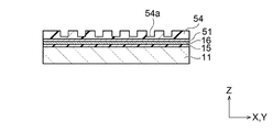
- the substrate 11 is prepared, and the easy-adhesion layer 15 and the adhesion layer 16 are sequentially formed on substantially the entire surface of the substrate 11.
- a roll coat, a gravure coat, a gravure reverse coat, a micro gravure coat, a slot die coat, a die coat, a knife coat, an inkjet coat, a dispenser coat, a kiss coat, and a spray coat may be used.
- a vapor deposition method, a sputtering method, or a plasma CVD method may be used as a method for forming the adhesion layer 16.
- the conductive layer 51 is formed on the close contact layer 16 in substantially the entire surface of the substrate 11.
- the thickness of the conductive layer 51 is 200 nm.
- the thickness of the conductive layer 51 is not limited to this, and can be appropriately selected in the range of 10 nm or more and 1000 nm or less.
- the conductive layer 51 is formed by a sputtering method using copper. As a method for forming the conductive layer 51, a plasma CVD method may be used.
- the photocurable insulating resist 52 is supplied on the adhesion layer 16 in substantially the entire surface of the substrate 11.
- the photocurable insulating resist 52 include organic resins such as epoxy resins.
- a transparent imprint mold 53 having a convex portion 53a is prepared (FIG. 8D), the mold 53 and the substrate 11 are brought close to each other, and a photocurable insulating resist is placed between the mold 53 and the substrate 11. Expand 52. Next, light irradiation is performed from the mold 53 side to cure the photocurable insulating resist 52, thereby forming the insulating layer 54. As a result, a trench 54a having a shape in which the convex portion 53a is transferred is formed on the surface of the insulating layer 54.
- the trench 54a has a planar shape pattern corresponding to the first-direction wiring 21 and the second-direction wiring 22.
- the direction in which the mold 53 is peeled from the insulating layer 54 is preferably the Y direction in which the longer first-direction wiring 21 extends.
- the insulating layer 54 may be formed by a photolithography method.
- the resist pattern is formed by the photolithography method so as to expose the conductive layer 51 corresponding to the first-direction wiring 21 and the second-direction wiring 22.
- a residue of the insulating material may remain at the bottom of the trench 54a of the insulating layer 54. Therefore, the residue of the insulating material is removed by performing a wet treatment using an organic solvent such as a permanganate solution or N-methyl-2-pyrrolidone, or a dry treatment using oxygen plasma.
- an organic solvent such as a permanganate solution or N-methyl-2-pyrrolidone
- the trench 54a of the insulating layer 54 is filled with the conductor 55.
- the conductive layer 51 is used as a seed layer, and the trench 54a of the insulating layer 54 is filled with copper by an electrolytic plating method.
- the conductor 55 has a planar shape corresponding to the first-direction wiring 21 and the second-direction wiring 22.
- the conductor 55 (first-direction wiring 21 and second).
- the area average particle size of the metal crystal 29 contained in the directional wiring 22) is set to 300 nm or more, and / or (ii) the surface roughness Ra of the conductor 55 (first direction wiring 21 and second direction wiring 22) is 100 nm. It can be as follows.
- the conductor 55 is made of copper and a copper sulfate bath containing copper sulfate as a main component is used as the plating solution
- various components such as copper sulfate, sulfuric acid, and a brightener containing a surfactant and the like contained in the plating solution are used.
- the growth rate of the crystal can be suppressed, and as a result, the area average particle size of the metal crystal 29 contained in the conductor 55 can be increased, and the surface roughness Ra of the conductor 55 can be suppressed.
- the metal crystals 29 contained in the conductor 55 are compared with the case where a general plating solution containing copper cyanide as a main component is used.
- the area average particle size of the conductor 55 can be increased and the outer surface of the conductor 55 can be made smooth.
- the insulating layer 54 is removed.
- the insulating layer 54 on the substrate 11 is removed by performing a wet treatment using an organic solvent such as a permanganate solution or N-methyl-2-pyrrolidone, or a dry treatment using oxygen plasma.
- the conductive layer 51 and the adhesive layer 16 on the surface of the substrate 11 are removed.
- the substrate 11 is subjected to a wet treatment using a copper etching solution such as an aqueous solution of ferric chloride, an aqueous solution of cupric chloride, an aqueous solution of ammonium peroxodisulfate, an aqueous solution of sodium peroxodisulfate, sulfuric acid, and a hydrogen peroxide solution.
- the conductive layer 51 and the adhesive layer 16 are etched so that the surface is exposed. After that, a blackening layer may be formed on the surface of the conductor 55 (first-direction wiring 21 and second-direction wiring 22).
- the protective layer 17 is formed so as to cover the easy-adhesion layer 15, the conductor 55, and the adhesion layer 16 on the substrate 11.
- the method for forming the protective layer 17 include roll coating, gravure coating, gravure reverse coating, micro gravure coating, slot die coating, die coating, knife coating, inkjet coating, dispenser coating, kiss coating, spray coating, screen printing, offset printing, and flexography. Printing may be used.
- the mesh wiring layer 20 includes the first direction wiring 21 and the second direction wiring 22.
- the feeding portion 40 may be formed by a part of the conductor 55.
- a flat plate-shaped power feeding unit 40 may be prepared separately, and the power feeding unit 40 may be electrically connected to the mesh wiring layer 20.
- the wiring board 10 is incorporated in an image display device 90 having a display 91.
- the wiring board 10 is arranged on the display 91.
- Examples of such an image display device 90 include mobile terminal devices such as smartphones and tablets.
- the mesh wiring layer 20 of the wiring board 10 is electrically connected to the wireless communication circuit 92 of the image display device 90 via the power feeding unit 40. In this way, radio waves of a predetermined frequency can be transmitted and received via the mesh wiring layer 20, and communication can be performed using the image display device 90.
- the area average particle diameter of the metal crystal 29 contained in the first-direction wiring 21 and the second-direction wiring 22 is 300 nm or more, and / or (ii).
- the surface roughness Ra of the first-direction wiring 21 and the second-direction wiring 22 is 100 nm or less.
- the development of mobile terminal devices for 5th generation communication that is, 5G (Generation) has been promoted.
- the mesh wiring layer 20 of the wiring board 10 is used as, for example, a 5G antenna (particularly a millimeter wave antenna)
- the radio waves (millimeter waves) transmitted and received by the mesh wiring layer 20 are, for example, the radio waves transmitted and received by the 4G antenna. It is higher frequency than that.
- the higher the frequency the more difficult it is for the current to flow in the central portion of the wiring, and the more the current flows on the surface of the wiring.
- the phenomenon in which an alternating current flows only on the surface when an alternating current is passed through the wiring is called the skin effect.
- the skin depth is the depth from the surface of the wiring that is attenuated 1 / e (about 0.37) times the current on the surface of the wiring through which the current is most likely to flow.
- the skin depth ⁇ (see FIG. 6) can generally be calculated by the following formula.
- ⁇ is the magnetic permeability (4 ⁇ ⁇ 10-7 [H / m] in vacuum)
- ⁇ is the conductivity of the conductors that make up the wiring (in the case of copper). means 5.8 ⁇ 10 7 [S / m ]).
- the smoother the surface of the mesh wiring layer 20, that is, the smaller the surface roughness Ra the more the skin resistance of the wiring is suppressed from increasing, and the transmission loss that occurs when transmitting and receiving radio waves can be reduced.
- the surface roughness Ra of the wiring when the surface roughness Ra of the wiring is large, the skin resistance of the wiring increases, and there is a possibility that transmission loss may occur when transmitting and receiving radio waves.
- the radio waves (millimeter waves) transmitted and received by the mesh wiring layer 20 are high frequencies
- the surface roughness Ra of the first direction wiring 21 and the second direction wiring 22 is suppressed to 100 nm or less, so that the first direction wiring 21 and the first direction wiring 21 and The skin resistance of the second direction wiring 22 can be reduced. Therefore, the skin resistance of the first-direction wiring 21 and the second-direction wiring 22 can prevent the current flow in the mesh wiring layer 20 from being obstructed.
- the line widths of the first direction wiring 21 and the second direction wiring 22 are 0.1 ⁇ m or more and 5.0 ⁇ m or less.
- the dielectric loss tangent of the substrate 11 is 0.002 or less, the dielectric generated during transmission / reception of radio waves is particularly high when the radio waves (millimeter waves) transmitted / received by the mesh wiring layer 20 are high frequencies. The loss can be reduced.
- the height of the height H 1 and the second direction line 22 of the first directional wires 21 H 2 can be raised.
- the adhesiveness between the substrate 11 and the first-direction wiring 21 and the second-direction wiring 22 can be improved. .. Further, since the adhesion layer 16 is formed on the easy-adhesion layer 15, the adhesion between the substrate 11 and the first-direction wiring 21 and the second-direction wiring 22 can be further improved.
- the protective layer 17 is formed on the substrate 11 so as to cover the first direction wiring 21 and the second direction wiring 22, the first direction wiring 21 and the second direction wiring 21 are formed. 22 can be protected from an external impact or the like.
- the mesh wiring layer 20 has a function as an antenna.
- the mesh wiring layer 20 as the antenna can be arranged on the outermost surface side of the image display device 90. Therefore, the communication performance can be improved as compared with the case where the antenna is built in the image display device 90. Further, since a plurality of mesh wiring layers 20 as antennas can be arranged in the plane of the image display device 90, the communication performance can be further improved.
- S11 means, for example, a value obtained by dividing the power reflected from the input terminal of the antenna by the power incident on the input terminal of the antenna. S11 can be measured using, for example, a network analyzer.
- the mesh wiring layer 20 has a function as an antenna has been described as an example, but the present invention is not limited to this.
- the mesh wiring layer 20 may perform functions such as hovering (a function that allows the user to operate without directly touching the display), fingerprint authentication, a heater, noise cut (shield), and the like. Even in such a case, the current can easily flow through the mesh wiring layer 20.
- both the first direction wiring 21 and the second direction wiring 22 have (i) an area average particle size of the metal crystal 29 contained in the first direction wiring 21 and the second direction wiring 22 of 300 nm or more. And / or (ii) the case where the surface roughness Ra of the first-direction wiring 21 and the second-direction wiring 22 is 100 nm or less has been described as an example, but the present invention is not limited to this.
- Only one of the first-direction wiring 21 and the second-direction wiring 22 has (i) an area average particle diameter of the metal crystal 29 contained in the first-direction wiring 21 and the second-direction wiring 22 of 300 nm or more, and / Or, (ii) the surface roughness Ra of the first-direction wiring 21 and the second-direction wiring 22 may be 100 nm or less.
- Example 1 A copper mesh pattern was produced on a PET film substrate by an electrolytic plating method using a plating solution containing copper sulfate as a main component. As a result, a wiring board 100 including the board 101 and the mesh wiring layer 102 was obtained (see FIG. 11).
- the size of the mesh wiring layer 102 was 2 mm in width ⁇ 7.5 mm in length, and a solid copper region 103 having the same width of 2 mm and a length of 1 mm was formed at the end portion having a length of 7.5 mm.
- the mesh wiring layer 102 and the solid copper region 103 are electrically connected.
- a width of 1 to 2 mm was opened from the solid copper region 103 to form a solid copper region (ground) 104 having a width of 6 mm or more and a length of 6 mm or more.
- the mesh wiring layer 102 has a grid pattern, and the solid regions 103 and 104 are solid (solid).
- the width of each wiring was set to 1 ⁇ m in both the width direction and the length direction of the mesh wiring layer 102.
- the height of each wiring was 1 ⁇ m, and the pitch of each wiring was 100 ⁇ m.
- the heights of the solid regions 103 and 104 were set to 1 ⁇ m.
- Example 2 The wiring board of Example 2 was produced in the same manner as in Example 1 except that the various components of the plating solution when producing the mesh wiring layer 102 and the solid regions 103 and 104 were different.
- Comparative Example 1 The wiring board of Comparative Example 1 was produced in the same manner as in Example 2 except that the various components of the plating solution when producing the mesh wiring layer 102 and the solid regions 103 and 104 were different.
- the area average particle diameter of the copper crystal and the surface roughness Ra of the wiring were measured, respectively.
- the area average particle size of the copper crystals was analyzed by the SEM-EBSD method.
- the surface roughness Ra of the wiring was measured using a laser microscope (VK-X250 (control unit), VK-X260 (measurement unit) manufactured by KEYENCE CORPORATION, laser wavelength 408 nm).
Landscapes
- Engineering & Computer Science (AREA)
- Microelectronics & Electronic Packaging (AREA)
- Manufacturing & Machinery (AREA)
- Manufacturing Of Printed Wiring (AREA)
- Structure Of Printed Boards (AREA)
- Details Of Aerials (AREA)
Priority Applications (7)
| Application Number | Priority Date | Filing Date | Title |
|---|---|---|---|
| KR1020227038545A KR20230004562A (ko) | 2020-05-01 | 2021-04-28 | 배선 기판 및 배선 기판의 제조 방법 |
| CN202180029449.9A CN115428259A (zh) | 2020-05-01 | 2021-04-28 | 配线基板和配线基板的制造方法 |
| US17/996,805 US12156337B2 (en) | 2020-05-01 | 2021-04-28 | Wiring board and method for manufacturing wiring board |
| JP2022518128A JP7667960B2 (ja) | 2020-05-01 | 2021-04-28 | 配線基板及び配線基板の製造方法 |
| EP21795893.3A EP4145621A4 (en) | 2020-05-01 | 2021-04-28 | PRINTED CIRCUIT BOARD AND METHOD FOR PRODUCING A PRINTED CIRCUIT BOARD |
| US18/889,578 US20250016928A1 (en) | 2020-05-01 | 2024-09-19 | Wiring board and method for manufacturing wiring board |
| JP2025065227A JP2025103028A (ja) | 2020-05-01 | 2025-04-10 | 配線基板及び配線基板の製造方法 |
Applications Claiming Priority (2)
| Application Number | Priority Date | Filing Date | Title |
|---|---|---|---|
| JP2020-081050 | 2020-05-01 | ||
| JP2020081050 | 2020-05-01 |
Related Child Applications (2)
| Application Number | Title | Priority Date | Filing Date |
|---|---|---|---|
| US17/996,805 A-371-Of-International US12156337B2 (en) | 2020-05-01 | 2021-04-28 | Wiring board and method for manufacturing wiring board |
| US18/889,578 Continuation US20250016928A1 (en) | 2020-05-01 | 2024-09-19 | Wiring board and method for manufacturing wiring board |
Publications (1)
| Publication Number | Publication Date |
|---|---|
| WO2021221119A1 true WO2021221119A1 (ja) | 2021-11-04 |
Family
ID=78374123
Family Applications (1)
| Application Number | Title | Priority Date | Filing Date |
|---|---|---|---|
| PCT/JP2021/017032 Ceased WO2021221119A1 (ja) | 2020-05-01 | 2021-04-28 | 配線基板及び配線基板の製造方法 |
Country Status (6)
| Country | Link |
|---|---|
| US (2) | US12156337B2 (https=) |
| EP (1) | EP4145621A4 (https=) |
| JP (2) | JP7667960B2 (https=) |
| KR (1) | KR20230004562A (https=) |
| CN (1) | CN115428259A (https=) |
| WO (1) | WO2021221119A1 (https=) |
Cited By (1)
| Publication number | Priority date | Publication date | Assignee | Title |
|---|---|---|---|---|
| CN114465008A (zh) * | 2022-02-15 | 2022-05-10 | 武汉大学 | 天线的制造方法 |
Families Citing this family (3)
| Publication number | Priority date | Publication date | Assignee | Title |
|---|---|---|---|---|
| TWI818257B (zh) * | 2021-05-07 | 2023-10-11 | 財團法人工業技術研究院 | 透明天線及其製作方法 |
| JP2022178307A (ja) * | 2021-05-20 | 2022-12-02 | イビデン株式会社 | プリント配線板 |
| TWI814207B (zh) * | 2022-01-12 | 2023-09-01 | 友達光電股份有限公司 | 天線模組及顯示裝置 |
Citations (9)
| Publication number | Priority date | Publication date | Assignee | Title |
|---|---|---|---|---|
| JP2005286891A (ja) * | 2004-03-30 | 2005-10-13 | Toto Ltd | アンテナ装置およびアンテナ装置の製造方法 |
| JP2008124446A (ja) * | 2006-10-19 | 2008-05-29 | National Institute Of Advanced Industrial & Technology | 導電パターン形成フィルムと、そのための導電パターン形成方法及び導電パターン形成装置 |
| JP2010239259A (ja) * | 2009-03-30 | 2010-10-21 | Sumitomo Osaka Cement Co Ltd | 透明平面アンテナ及び粘着剤層付き透明平面アンテナ |
| JP2011066610A (ja) | 2009-09-16 | 2011-03-31 | Dainippon Printing Co Ltd | 透明アンテナ |
| JP2014110514A (ja) * | 2012-11-30 | 2014-06-12 | Toppan Forms Co Ltd | アンテナ構造体、通信機器及びアンテナ構造体の製造方法 |
| JP5636735B2 (ja) | 2009-09-24 | 2014-12-10 | 大日本印刷株式会社 | 透明アンテナ用エレメント及び透明アンテナ |
| JP5695947B2 (ja) | 2010-03-25 | 2015-04-08 | ソニーモバイルコミュニケーションズ株式会社 | アンテナ装置および携帯機器 |
| WO2016104723A1 (ja) * | 2014-12-26 | 2016-06-30 | 株式会社フジクラ | 配線体、配線基板、タッチセンサ、及び配線体の製造方法 |
| JP2017185690A (ja) * | 2016-04-05 | 2017-10-12 | 住友金属鉱山株式会社 | 導電性基板、導電性基板の製造方法 |
Family Cites Families (9)
| Publication number | Priority date | Publication date | Assignee | Title |
|---|---|---|---|---|
| JPS5392930A (en) | 1977-01-26 | 1978-08-15 | Agency Of Ind Science & Technol | Combustion system |
| US20050079903A1 (en) * | 2002-04-18 | 2005-04-14 | Hirokazu Taketomi | Cell phone and built-in antenna thereof |
| WO2005069713A1 (ja) * | 2004-01-13 | 2005-07-28 | Dai Nippon Printing Co., Ltd. | 電磁波シールドシート及びその製造方法 |
| US8237213B2 (en) * | 2010-07-15 | 2012-08-07 | Micron Technology, Inc. | Memory arrays having substantially vertical, adjacent semiconductor structures and the formation thereof |
| JP5927927B2 (ja) * | 2012-01-18 | 2016-06-01 | 新日鐵住金株式会社 | 現地溶接性に優れるラインパイプ用高強度熱延鋼板およびその製造方法 |
| WO2014156827A1 (ja) * | 2013-03-27 | 2014-10-02 | 富士フイルム株式会社 | 導電シートおよびその製造方法、タッチパネル |
| WO2016143201A1 (ja) * | 2015-03-06 | 2016-09-15 | コニカミノルタ株式会社 | 透明電極とその製造方法及び有機エレクトロルミネッセンス素子 |
| TWI652698B (zh) * | 2016-03-08 | 2019-03-01 | 日商藤倉股份有限公司 | 導線體、導線基板及觸控感測器 |
| TWI681872B (zh) * | 2017-07-18 | 2020-01-11 | 日商旭化成股份有限公司 | 具有導電性圖案區域之構造體及其製造方法、積層體及其製造方法 |
-
2021
- 2021-04-28 JP JP2022518128A patent/JP7667960B2/ja active Active
- 2021-04-28 WO PCT/JP2021/017032 patent/WO2021221119A1/ja not_active Ceased
- 2021-04-28 US US17/996,805 patent/US12156337B2/en active Active
- 2021-04-28 KR KR1020227038545A patent/KR20230004562A/ko not_active Ceased
- 2021-04-28 EP EP21795893.3A patent/EP4145621A4/en active Pending
- 2021-04-28 CN CN202180029449.9A patent/CN115428259A/zh active Pending
-
2024
- 2024-09-19 US US18/889,578 patent/US20250016928A1/en active Pending
-
2025
- 2025-04-10 JP JP2025065227A patent/JP2025103028A/ja active Pending
Patent Citations (9)
| Publication number | Priority date | Publication date | Assignee | Title |
|---|---|---|---|---|
| JP2005286891A (ja) * | 2004-03-30 | 2005-10-13 | Toto Ltd | アンテナ装置およびアンテナ装置の製造方法 |
| JP2008124446A (ja) * | 2006-10-19 | 2008-05-29 | National Institute Of Advanced Industrial & Technology | 導電パターン形成フィルムと、そのための導電パターン形成方法及び導電パターン形成装置 |
| JP2010239259A (ja) * | 2009-03-30 | 2010-10-21 | Sumitomo Osaka Cement Co Ltd | 透明平面アンテナ及び粘着剤層付き透明平面アンテナ |
| JP2011066610A (ja) | 2009-09-16 | 2011-03-31 | Dainippon Printing Co Ltd | 透明アンテナ |
| JP5636735B2 (ja) | 2009-09-24 | 2014-12-10 | 大日本印刷株式会社 | 透明アンテナ用エレメント及び透明アンテナ |
| JP5695947B2 (ja) | 2010-03-25 | 2015-04-08 | ソニーモバイルコミュニケーションズ株式会社 | アンテナ装置および携帯機器 |
| JP2014110514A (ja) * | 2012-11-30 | 2014-06-12 | Toppan Forms Co Ltd | アンテナ構造体、通信機器及びアンテナ構造体の製造方法 |
| WO2016104723A1 (ja) * | 2014-12-26 | 2016-06-30 | 株式会社フジクラ | 配線体、配線基板、タッチセンサ、及び配線体の製造方法 |
| JP2017185690A (ja) * | 2016-04-05 | 2017-10-12 | 住友金属鉱山株式会社 | 導電性基板、導電性基板の製造方法 |
Non-Patent Citations (1)
| Title |
|---|
| See also references of EP4145621A4 |
Cited By (1)
| Publication number | Priority date | Publication date | Assignee | Title |
|---|---|---|---|---|
| CN114465008A (zh) * | 2022-02-15 | 2022-05-10 | 武汉大学 | 天线的制造方法 |
Also Published As
| Publication number | Publication date |
|---|---|
| US20250016928A1 (en) | 2025-01-09 |
| US20230062683A1 (en) | 2023-03-02 |
| JPWO2021221119A1 (https=) | 2021-11-04 |
| CN115428259A (zh) | 2022-12-02 |
| US12156337B2 (en) | 2024-11-26 |
| KR20230004562A (ko) | 2023-01-06 |
| JP7667960B2 (ja) | 2025-04-24 |
| JP2025103028A (ja) | 2025-07-08 |
| EP4145621A1 (en) | 2023-03-08 |
| EP4145621A4 (en) | 2024-04-03 |
| TW202147687A (zh) | 2021-12-16 |
Similar Documents
| Publication | Publication Date | Title |
|---|---|---|
| JP7667960B2 (ja) | 配線基板及び配線基板の製造方法 | |
| KR102672229B1 (ko) | 배선 기판 및 배선 기판의 제조 방법 | |
| JP7587758B2 (ja) | 配線基板および配線基板の製造方法 | |
| TWI905166B (zh) | 配線基板及配線基板之製造方法 | |
| CN116325348A (zh) | 布线基板和布线基板的制造方法 | |
| JP2022163867A (ja) | 配線基板、モジュール、配線基板の製造方法およびモジュールの製造方法 | |
| TWI920081B (zh) | 配線基板及配線基板之製造方法 | |
| JP2025061455A (ja) | 配線基板および配線基板の製造方法 | |
| JP7482390B2 (ja) | 配線基板及び配線基板の製造方法 | |
| JP7593055B2 (ja) | 配線基板および配線基板の製造方法 | |
| JP7528717B2 (ja) | 配線基板および配線基板の製造方法 | |
| JP2026071256A (ja) | 配線基板、モジュール及び画像表示装置 |
Legal Events
| Date | Code | Title | Description |
|---|---|---|---|
| 121 | Ep: the epo has been informed by wipo that ep was designated in this application |
Ref document number: 21795893 Country of ref document: EP Kind code of ref document: A1 |
|
| ENP | Entry into the national phase |
Ref document number: 2022518128 Country of ref document: JP Kind code of ref document: A |
|
| ENP | Entry into the national phase |
Ref document number: 2021795893 Country of ref document: EP Effective date: 20221201 |
|
| NENP | Non-entry into the national phase |
Ref country code: DE |
|
| WWR | Wipo information: refused in national office |
Ref document number: 1020227038545 Country of ref document: KR |