WO2021220852A1 - 信号処理装置、信号処理方法、及び表示装置 - Google Patents
信号処理装置、信号処理方法、及び表示装置 Download PDFInfo
- Publication number
- WO2021220852A1 WO2021220852A1 PCT/JP2021/015794 JP2021015794W WO2021220852A1 WO 2021220852 A1 WO2021220852 A1 WO 2021220852A1 JP 2021015794 W JP2021015794 W JP 2021015794W WO 2021220852 A1 WO2021220852 A1 WO 2021220852A1
- Authority
- WO
- WIPO (PCT)
- Prior art keywords
- signal processing
- panel
- unit
- information
- panel unit
- Prior art date
- Legal status (The legal status is an assumption and is not a legal conclusion. Google has not performed a legal analysis and makes no representation as to the accuracy of the status listed.)
- Ceased
Links
Images




Classifications
-
- G—PHYSICS
- G09—EDUCATION; CRYPTOGRAPHY; DISPLAY; ADVERTISING; SEALS
- G09G—ARRANGEMENTS OR CIRCUITS FOR CONTROL OF INDICATING DEVICES USING STATIC MEANS TO PRESENT VARIABLE INFORMATION
- G09G3/00—Control arrangements or circuits, of interest only in connection with visual indicators other than cathode-ray tubes
- G09G3/20—Control arrangements or circuits, of interest only in connection with visual indicators other than cathode-ray tubes for presentation of an assembly of a number of characters, e.g. a page, by composing the assembly by combination of individual elements arranged in a matrix no fixed position being assigned to or needed to be assigned to the individual characters or partial characters
- G09G3/22—Control arrangements or circuits, of interest only in connection with visual indicators other than cathode-ray tubes for presentation of an assembly of a number of characters, e.g. a page, by composing the assembly by combination of individual elements arranged in a matrix no fixed position being assigned to or needed to be assigned to the individual characters or partial characters using controlled light sources
- G09G3/30—Control arrangements or circuits, of interest only in connection with visual indicators other than cathode-ray tubes for presentation of an assembly of a number of characters, e.g. a page, by composing the assembly by combination of individual elements arranged in a matrix no fixed position being assigned to or needed to be assigned to the individual characters or partial characters using controlled light sources using electroluminescent panels
- G09G3/32—Control arrangements or circuits, of interest only in connection with visual indicators other than cathode-ray tubes for presentation of an assembly of a number of characters, e.g. a page, by composing the assembly by combination of individual elements arranged in a matrix no fixed position being assigned to or needed to be assigned to the individual characters or partial characters using controlled light sources using electroluminescent panels semiconductive, e.g. using light-emitting diodes [LED]
- G09G3/3208—Control arrangements or circuits, of interest only in connection with visual indicators other than cathode-ray tubes for presentation of an assembly of a number of characters, e.g. a page, by composing the assembly by combination of individual elements arranged in a matrix no fixed position being assigned to or needed to be assigned to the individual characters or partial characters using controlled light sources using electroluminescent panels semiconductive, e.g. using light-emitting diodes [LED] organic, e.g. using organic light-emitting diodes [OLED]
-
- G—PHYSICS
- G09—EDUCATION; CRYPTOGRAPHY; DISPLAY; ADVERTISING; SEALS
- G09G—ARRANGEMENTS OR CIRCUITS FOR CONTROL OF INDICATING DEVICES USING STATIC MEANS TO PRESENT VARIABLE INFORMATION
- G09G2320/00—Control of display operating conditions
- G09G2320/02—Improving the quality of display appearance
- G09G2320/029—Improving the quality of display appearance by monitoring one or more pixels in the display panel, e.g. by monitoring a fixed reference pixel
-
- G—PHYSICS
- G09—EDUCATION; CRYPTOGRAPHY; DISPLAY; ADVERTISING; SEALS
- G09G—ARRANGEMENTS OR CIRCUITS FOR CONTROL OF INDICATING DEVICES USING STATIC MEANS TO PRESENT VARIABLE INFORMATION
- G09G2320/00—Control of display operating conditions
- G09G2320/04—Maintaining the quality of display appearance
- G09G2320/041—Temperature compensation
-
- G—PHYSICS
- G09—EDUCATION; CRYPTOGRAPHY; DISPLAY; ADVERTISING; SEALS
- G09G—ARRANGEMENTS OR CIRCUITS FOR CONTROL OF INDICATING DEVICES USING STATIC MEANS TO PRESENT VARIABLE INFORMATION
- G09G2320/00—Control of display operating conditions
- G09G2320/06—Adjustment of display parameters
- G09G2320/0626—Adjustment of display parameters for control of overall brightness
-
- G—PHYSICS
- G09—EDUCATION; CRYPTOGRAPHY; DISPLAY; ADVERTISING; SEALS
- G09G—ARRANGEMENTS OR CIRCUITS FOR CONTROL OF INDICATING DEVICES USING STATIC MEANS TO PRESENT VARIABLE INFORMATION
- G09G2330/00—Aspects of power supply; Aspects of display protection and defect management
- G09G2330/02—Details of power systems and of start or stop of display operation
- G09G2330/021—Power management, e.g. power saving
-
- G—PHYSICS
- G09—EDUCATION; CRYPTOGRAPHY; DISPLAY; ADVERTISING; SEALS
- G09G—ARRANGEMENTS OR CIRCUITS FOR CONTROL OF INDICATING DEVICES USING STATIC MEANS TO PRESENT VARIABLE INFORMATION
- G09G2330/00—Aspects of power supply; Aspects of display protection and defect management
- G09G2330/02—Details of power systems and of start or stop of display operation
- G09G2330/021—Power management, e.g. power saving
- G09G2330/023—Power management, e.g. power saving using energy recovery or conservation
-
- G—PHYSICS
- G09—EDUCATION; CRYPTOGRAPHY; DISPLAY; ADVERTISING; SEALS
- G09G—ARRANGEMENTS OR CIRCUITS FOR CONTROL OF INDICATING DEVICES USING STATIC MEANS TO PRESENT VARIABLE INFORMATION
- G09G2330/00—Aspects of power supply; Aspects of display protection and defect management
- G09G2330/02—Details of power systems and of start or stop of display operation
- G09G2330/028—Generation of voltages supplied to electrode drivers in a matrix display other than LCD
-
- G—PHYSICS
- G09—EDUCATION; CRYPTOGRAPHY; DISPLAY; ADVERTISING; SEALS
- G09G—ARRANGEMENTS OR CIRCUITS FOR CONTROL OF INDICATING DEVICES USING STATIC MEANS TO PRESENT VARIABLE INFORMATION
- G09G2360/00—Aspects of the architecture of display systems
- G09G2360/14—Detecting light within display terminals, e.g. using a single or a plurality of photosensors
- G09G2360/145—Detecting light within display terminals, e.g. using a single or a plurality of photosensors the light originating from the display screen
-
- G—PHYSICS
- G09—EDUCATION; CRYPTOGRAPHY; DISPLAY; ADVERTISING; SEALS
- G09G—ARRANGEMENTS OR CIRCUITS FOR CONTROL OF INDICATING DEVICES USING STATIC MEANS TO PRESENT VARIABLE INFORMATION
- G09G2360/00—Aspects of the architecture of display systems
- G09G2360/16—Calculation or use of calculated indices related to luminance levels in display data
-
- G—PHYSICS
- G09—EDUCATION; CRYPTOGRAPHY; DISPLAY; ADVERTISING; SEALS
- G09G—ARRANGEMENTS OR CIRCUITS FOR CONTROL OF INDICATING DEVICES USING STATIC MEANS TO PRESENT VARIABLE INFORMATION
- G09G5/00—Control arrangements or circuits for visual indicators common to cathode-ray tube indicators and other visual indicators
- G09G5/02—Control arrangements or circuits for visual indicators common to cathode-ray tube indicators and other visual indicators characterised by the way in which colour is displayed
-
- G—PHYSICS
- G09—EDUCATION; CRYPTOGRAPHY; DISPLAY; ADVERTISING; SEALS
- G09G—ARRANGEMENTS OR CIRCUITS FOR CONTROL OF INDICATING DEVICES USING STATIC MEANS TO PRESENT VARIABLE INFORMATION
- G09G5/00—Control arrangements or circuits for visual indicators common to cathode-ray tube indicators and other visual indicators
- G09G5/10—Intensity circuits
-
- H—ELECTRICITY
- H04—ELECTRIC COMMUNICATION TECHNIQUE
- H04N—PICTORIAL COMMUNICATION, e.g. TELEVISION
- H04N5/00—Details of television systems
- H04N5/44—Receiver circuitry for the reception of television signals according to analogue transmission standards
- H04N5/57—Control of contrast or brightness
-
- H—ELECTRICITY
- H10—SEMICONDUCTOR DEVICES; ELECTRIC SOLID-STATE DEVICES NOT OTHERWISE PROVIDED FOR
- H10K—ORGANIC ELECTRIC SOLID-STATE DEVICES
- H10K59/00—Integrated devices, or assemblies of multiple devices, comprising at least one organic light-emitting element covered by group H10K50/00
- H10K59/30—Devices specially adapted for multicolour light emission
- H10K59/35—Devices specially adapted for multicolour light emission comprising red-green-blue [RGB] subpixels
- H10K59/351—Devices specially adapted for multicolour light emission comprising red-green-blue [RGB] subpixels comprising more than three subpixels, e.g. red-green-blue-white [RGBW]
Definitions
- the present technology relates to a signal processing device, a signal processing method, and a display device, and more particularly to a signal processing device, a signal processing method, and a display device capable of performing control suitable for an application.
- Patent Document 1 discloses a technique for reducing power consumption as a technique for an OLED display device.
- display devices such as self-luminous display devices are required to perform control suitable for applications such as realization of low power consumption.
- This technology was made in view of such a situation, and makes it possible to perform control suitable for the application.
- the signal processing device on one aspect of the present technology is measured as a first information regarding the color of the image displayed on the panel unit, a second information regarding the screen brightness of the panel unit, and a physical quantity related to the panel unit.
- Signal processing that acquires at least one of the third pieces of information and, based on the acquired information, adaptively controls the voltage for driving the panel unit according to the load and application of the panel unit. It is a signal processing device including a unit.
- the signal processing device relates to the first information regarding the color of the image displayed on the panel unit, the second information regarding the screen brightness of the panel unit, and the panel unit. At least one of the third pieces of information measured as a physical quantity is acquired, and based on the acquired information, the voltage for driving the panel portion is adaptively applied according to the load and application of the panel portion. It is a signal processing method to control.
- the first information regarding the color of the image displayed on the panel unit the second information regarding the screen brightness of the panel unit, and the panel unit.
- At least one of the third pieces of information measured as a physical quantity related to the above is acquired, and based on the acquired information, the voltage for driving the panel unit is determined according to the load and application of the panel unit. It is adaptively controlled.
- the display device on one side of the present technology includes a panel unit and a signal processing unit, and the signal processing unit provides first information regarding the color of the image displayed on the panel unit, the brightness of the screen of the panel unit.
- the signal processing unit provides first information regarding the color of the image displayed on the panel unit, the brightness of the screen of the panel unit.
- the second information related to the above and the third information measured as a physical quantity related to the panel unit at least one piece of information is acquired, and the voltage for driving the panel unit is calculated based on the acquired information.
- This is a display device that is adaptively controlled according to the load and application of the panel unit.
- the display device on one aspect of the present technology, it is measured as the first information regarding the color of the image displayed on the panel unit, the second information regarding the screen brightness of the panel unit, and the physical quantity related to the panel unit. At least one of the third pieces of information is acquired, and based on the acquired information, the voltage for driving the panel unit is adaptively controlled according to the load and application of the panel unit. ..
- the signal processing device and the display device on one aspect of the present technology may be independent devices or internal blocks constituting one device.
- the OLED display device As a technology for reducing power consumption, a technology for adjusting the gamma voltage and the drive voltage of the reference by measuring the APL (Average Picture Level) and the maximum gradation value of the image is known.
- APL Average Picture Level
- the judgment process is performed using only the measured APL and the maximum gradation value, so it is not possible to consider the difference in the amount of current with respect to the light emission of each pixel arranged on the display panel. , It is not possible to grasp the load of the entire screen of the display panel.
- each pixel arranged in a two-dimensional shape is composed of four sub-pixels of white (W), red (R), green (G), and blue (B), or red (R).
- Green (G), and blue (B) can be composed of three sub-pixels.
- a method in which each pixel is a WRGB pixel is referred to as a WRGB method
- a method in which each pixel is an RGB pixel is referred to as an RGB method.
- each pixel of the display panel corresponding to the WRGB system the current applied to each emission level of white (W), red (R), green (G), and blue (B) is different.
- the current applied to each of the red (R), green (G), and blue (B) light emission levels is different. Therefore, when grasping the load of the entire screen of the display panel, it is difficult to accurately grasp (predict) unless information on colors is also taken into consideration.
- FIG. 1 shows the relationship between the color component of each pixel and the current value.
- the horizontal axis represents the color of the sub-pixel (White, Red, Green, Blue) and the color when the sub-pixel is lit in two colors (Yellow, Cyan, Magenta), and the vertical axis represents the panel drive current value. Shown. In each pixel, when the sub-pixels R and G are lit, the color becomes yellow (Y), when the sub-pixels R and B are lit, the color becomes magenta (M), and when the sub-pixels G and B are lit, the color becomes cyan (C). )become.
- the current value of each color component is represented by a bar extending in the vertical direction for each color component. From this bar graph, it can be seen that the current value differs for each color component. In particular, in yellow (Y), magenta (M), and cyan (C), since the sub-pixels are lit in two colors, the increase in the current value becomes remarkable.
- a timing controller (T-CON: Timing Controller) is provided for the display panel.
- T-CON Timing Controller
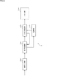
- FIG. 2 shows a configuration when the function is realized by the timing controller 13 provided for the panel unit 14.
- the timing controller 13 controls the panel drive voltage via the power supply unit 12, but since the video signal processed by the signal processing unit 11 is held in the frame memory 22, the voltage drive and the video It is difficult to control the signals at the same time.
- FIG. 3 shows a configuration in which a function is realized by a signal processing unit 11 configured as a video SoC or the like on a set board.
- the timing controller 13 since the signal processing unit 11 controls the panel drive voltage via the power supply unit 12, the timing controller 13 has a margin for the frame buffer of the frame memory 22.
- FIG. 4 shows an example of the screen brightness of the panel unit 14 due to the panel drive voltage.
- the horizontal axis corresponds to the height position of the screen of the panel unit 14, the substantially central portion corresponds to the central portion of the screen in the height direction, and the left side of the horizontal axis is closer to the upper part of the screen. It shows that the closer to the right side of the horizontal axis, the closer to the bottom of the screen.
- the vertical axis shows the brightness, and the upper side of the vertical axis shows the higher brightness, while the lower side of the vertical axis shows the lower brightness.
- the thick lines L11 to L13 represent the screen brightness according to the panel drive voltage.
- the thick line L11 represents the case where the panel drive voltage is V11
- the thick line L12 represents the case where the panel drive voltage is V12
- the thick line L13 represents the case where the panel drive voltage is V13.
- these panel drive voltages have a relationship of V11> V12> V13.
- the voltage value of the panel drive voltage is low as shown by the thick line L12 and the thick line L13 (V12 and V13 are higher than V11). If the value is low), the brightness of the central part of the screen of the panel unit 14 does not increase, and a difference in brightness occurs.
- the panel drive voltage indicated by the thick line L12 is V12
- the central portion of the screen has a predetermined ratio such as several percent (for example, about 7% in FIG. 4) as compared with the portion near the upper part of the screen or the lower part of the screen. The brightness is decreasing.
- the panel drive voltage is increased to V11 as shown by the thick line L11 in FIG. 4).
- FIG. 5 schematically shows the relationship between the power supply wiring of the panel unit 14 and the current supply.
- the image of the window pattern (white area in the figure) as shown in A of FIG. 5 is displayed on the panel unit 14, the relationship between the power supply wiring and the current supply of the panel unit 14 is as shown in B of FIG. Become a relationship.
- the rectangular broken line of B in FIG. 5 corresponds to the window pattern of A in FIG.
- FIG. 6 shows a configuration example of an embodiment of a display device to which the present technology is applied.
- the display device 1 is a self-luminous display device such as an OLED display device having an OLED panel.
- the display device 1 is configured as a television receiver or the like.
- the display device 1 is composed of a signal input unit 110, a signal processing unit 111, a power supply unit 112, a panel drive unit 113, and a panel unit 114.
- the signal input unit 110 is composed of a tuner connected to an antenna, a communication module that can be connected to a communication network such as the Internet, an input interface conforming to a predetermined standard, and the like.
- the signal input unit 110 records broadcast content transmitted by terrestrial broadcasting, satellite broadcasting, etc., communication content streamed via a communication network such as the Internet, or a recording medium such as an optical disk or semiconductor memory, a recorder, or the like. Video signals of various contents such as recorded contents are supplied to the signal processing unit 111.
- the signal processing unit 111 performs video signal processing on the video signal of the content supplied from the signal input unit 110, and supplies the video signal obtained as a result to the panel drive unit 113. Further, the signal processing unit 111 controls the panel drive voltage for the panel drive unit 113 to drive the panel unit 114 via the power supply unit 112.
- the panel drive unit 113 drives the panel unit 114 based on the video signal supplied from the signal processing unit 111 and the panel drive voltage controlled by the signal processing unit 111. Further, the panel drive unit 113 measures the surface temperature and the amount of current of the panel unit 114, and supplies the measurement result to the signal processing unit 111.
- the panel unit 114 is a display panel such as an OLED panel.
- the panel unit 114 displays images according to the image signals of various contents according to the drive from the panel drive unit 113.
- the OLED panel is a display panel in which pixels including an OLED element as a self-luminous element are arranged two-dimensionally.
- An OLED Organic Light Emitting Diode
- An OLED is a light emitting element having a structure in which an organic light emitting material is sandwiched between a cathode and an anode, and constitutes pixels (display pixels) arranged two-dimensionally on an OLED panel. There is.
- each pixel is composed of four sub-pixels of white (W), red (R), green (G), and blue (B) in the case of the RGB system, and is of the RGB system. In the case, it is composed of three sub-pixels of red (R), green (G), and blue (B).
- the minimum configuration is shown for the sake of simplification of the explanation, but there are other devices such as a sound signal processing circuit that processes a sound signal and a speaker that outputs a sound corresponding to the sound signal. Circuits and devices may be included.
- FIG. 7 shows a detailed configuration example of the signal processing unit 111 of FIG.
- the signal processing unit 111 includes a W conversion unit 131, a hue detection unit 132, a saturation detection unit 133, a brightness detection unit 134, an APL detection unit 135, and a voltage control unit 136.
- the video signal from the signal input unit 110 is supplied to the W conversion unit 131 and the APL detection unit 135, respectively. Further, the video signal is supplied to the panel drive unit 113.
- the W conversion unit 131 performs White conversion processing on the video signal input therein, and the video signal after W conversion obtained as a result of the processing is subjected to the hue detection unit 132, the saturation detection unit 133, and the brightness detection unit 134. Supply to each.
- the hue detection unit 132 performs hue detection processing on the video signal supplied from the W conversion unit 131, and supplies the hue information obtained as a result of the processing to the voltage control unit 136. In this hue detection process, the hue (H: Hue) is detected among the components of the color space (HSV color space) of the video signal.
- the saturation detection unit 133 performs saturation detection processing on the video signal supplied from the W conversion unit 131, and supplies the saturation information obtained as a result of the processing to the voltage control unit 136.
- saturation S: Saturation
- HSV color space the color space
- the brightness detection unit 134 performs brightness detection processing on the video signal supplied from the W conversion unit 131, and supplies the brightness information obtained as a result of the processing to the voltage control unit 136.
- the brightness (V: Value) is detected among the components of the color space (HSV color space) of the video signal.
- the APL detection unit 135 performs APL detection processing on the video signal input therein, and supplies the APL information obtained as a result of the processing to the voltage control unit 136.
- the average pixel level (APL: Average Pixel Level) is detected based on the video signal.
- the average pixel level (APL) is a value that is an index of the brightness of the entire screen of the panel unit 114.
- Hue information from the hue detection unit 132, saturation information from the saturation detection unit 133, brightness information from the brightness detection unit 134, and APL information from the APL detection unit 135 are supplied to the voltage control unit 136, respectively. ..
- the voltage control unit 136 is also supplied with temperature information and current information from the panel drive unit 113.
- the voltage control unit 136 loads the panel drive voltage for driving the panel unit 114 based on at least one of the hue information, the saturation information, the brightness information, the APL information, the temperature information, and the current information. And adaptively control according to the application.
- the power supply unit 112 variably controls the panel drive voltage according to the control from the voltage control unit 136 and supplies it to the panel drive unit 113, so that the panel unit 114 is driven based on the applied panel drive voltage.
- the voltage control unit 136 controls the HSV color space based on the hue information, the saturation information, and the brightness information. Details of the control related to the HSV color space will be described later with reference to FIGS. 8 to 11. Further, the voltage control unit 136 controls the brightness curve based on the APL information. Details of the control related to the luminance curve will be described later with reference to FIGS. 12 and 13. Further, the voltage control unit 136 controls the panel drive voltage based on the temperature information and the current information.
- the panel drive unit 113 includes a panel temperature measurement unit 151 and a panel current measurement unit 152.
- the panel temperature measuring unit 151 supplies the voltage control unit 136 with temperature information indicating the surface temperature of the panel unit 114 measured by a temperature sensor or the like provided for the panel unit 114.
- a temperature sensor or the like provided for the panel unit 114.
- a configuration example of the temperature sensor will be described later with reference to FIGS. 14 and 15.
- the panel current measuring unit 152 supplies the voltage control unit 136 with current information indicating the amount of current of the panel drive voltage applied to the panel unit 114 measured by a current sensor or the like provided for the panel unit 114.
- a current sensor or the like provided for the panel unit 114.
- FIG. 8 shows an example of the color expression range of the video signal.
- the color expression range of the video signal is represented by the HSV color space.
- the HSV color space is a color space composed of three components: hue (H: Hue), saturation (S: Saturation), and lightness (V: Value).
- hue means the type of color
- saturation means the vividness of the color
- lightness means the brightness of the color.
- the HSV color space is represented by a cylinder 51.
- the azimuth direction shows the hue H
- the radial direction shows the saturation S
- the axial direction shows the lightness V.
- a part of the cross section of hue H in the HSV color space is cut out and shown.
- the cylinder 51 in the HSV color space is the four sub-pixels of white (W), red (R), green (G), and blue (B) in each pixel of the WRGB system, or red (red) in each pixel of the RGB system. It corresponds to the range of colors that can be expressed by the three sub-pixels of R), green (G), and blue (B).
- the current applied to each pixel in the panel unit 114 is different for each emission level of the WRGB method or the RGB method. Therefore, in order to accurately grasp the load of the panel unit 114, it is necessary to add color information.
- FIG. 9 shows an example of gain control linked to hue H.
- the horizontal axis represents the hue H and the vertical axis represents the hue-linked gain.
- Hue H on the horizontal axis is represented by a value in the range of 0 ° to 360 °. Specifically, hue 0 ° is red, hue 60 ° is yellow, hue 120 ° is green, hue 180 ° is cyan, hue 240 ° is blue, and hue 300 ° is magenta.
- the weight of the current load is grasped for each hue H according to the characteristics of the OLED element of each pixel.
- complementary colors such as yellow (Y: Yellow), cyan (C: Cyan), and magenta (M: Magenta) light up two RGB sub-pixels in each pixel, so the RGB sub-pixels are turned on. Since the load is larger than when it is lit in a single color, it is necessary to adjust the weight.
- the hue interlocking gain according to the hue H is shown by the thick line L21 represented by the triangular wave, but it is a complementary color of yellow (Y), cyan (C), and magenta (M).
- the hue-linked gain is 1.0 times, and the weight is changed for other colors.
- the voltage control unit 136 adaptively controls the panel drive voltage by adjusting the weight using the hue interlocking gain according to the hue information from the hue detection unit 132. Thereby, for example, when the RGB sub-pixels are lit in two colors by the complementary color video signal, the weight can be adjusted to suppress the load.
- FIG. 10 shows an example of gain control linked to saturation S.
- the horizontal axis represents the saturation S
- the vertical axis represents the saturation-linked gain.
- Saturation S on the horizontal axis is represented by a value in the range of 0 to 1 (0% to 100%). Specifically, it becomes 0 in achromatic color according to the distance from the central axis (achromatic color axis) of the cylinder 51 in the HSV color space, and increases as the distance from the achromatic axis becomes maximum in pure color or the like.
- the weight is controlled according to the shade of color.
- the luminous efficiency of the sub-pixel W is better than the luminous efficiency of the other sub-pixels R, G, and B in each pixel. Therefore, the darker the color, the more the weight needs to be considered.
- the saturation-linked gain according to the saturation S is indicated by a thick line L31 represented by a straight line rising to the right, but as the saturation S increases, the gain also increases with a constant inclination, and the saturation increases. It is possible to change the weight in the direction.
- This saturation-linked gain can be referred to as a high-saturation-linked gain because the higher the saturation, the larger the gain.
- the panel drive voltage is adaptively controlled by adjusting the weight using the saturation interlocking gain according to the saturation information from the saturation detection unit 133.
- the saturation interlocking gain according to the saturation information from the saturation detection unit 133.
- FIG. 11 shows an example of gain control linked to the brightness V.
- the horizontal axis represents the brightness V
- the vertical axis represents the brightness-linked gain.
- Brightness V on the horizontal axis is represented by a value in the range of 0 to 1 (0% to 100%). Specifically, in the cylinder 51 of the HSV color space, the brightness increases in the height direction, and the higher the lightness, the brighter the lightness, while the lower the lightness, the darker the lightness.
- the weight is controlled according to the signal level of the video signal. That is, in each pixel, when the light emission level is simply increased, the load is increased by that amount, so that the brightness-linked gain is controlled as a mechanism linked to the load.
- the brightness-linked gain according to the brightness V is indicated by a thick line L41 represented by a straight line rising to the right, but as the brightness V increases, the gain also increases with a constant inclination, and the weight in the brightness direction increases. Can be changed.
- This brightness-linked gain can be referred to as a high-brightness-linked gain because the higher the brightness, the larger the gain.
- the panel drive voltage is adaptively controlled by adjusting the weight using the brightness interlocking gain according to the brightness information from the brightness detection unit 134. As a result, when the light emission level of the pixel is high, the weight can be adjusted to suppress the load.
- the voltage control unit 136 has gain (hue) based on information (hue information, saturation information, lightness information) related to each component (hue, saturation, lightness) of the color space (HSV color space) of the video signal.
- gain based on information (hue information, saturation information, lightness information) related to each component (hue, saturation, lightness) of the color space (HSV color space) of the video signal.
- an OLED panel has a feature that the brightness decreases according to the brightness of the entire screen. The reason is that in the OLED panel, the pixels including the OLED element are arranged two-dimensionally, and as the light emitting area expands, the amount of current in the entire screen increases. Therefore, in the OLED panel, when the light emitting area is small, it can be made to shine brightly, but when the light emitting area is large, the total light emitting amount is reduced.
- the display device 1 In order to consider such characteristics of the OLED display device, in the display device 1, it is necessary to predict the load of the panel unit 114 according to the average pixel level (APL) indicating the brightness of the entire screen of the panel unit 114. Yes, it is necessary to weight according to the light emitting area.
- APL average pixel level
- FIGS. 12 and 13 show an example of the relationship between the average pixel level (APL) and the emission brightness in the panel unit 114.
- the horizontal axis represents the average pixel level (APL) and the vertical axis represents the luminance (Luminance).
- the average pixel level (APL) on the horizontal axis is represented by a value in the range 0-100%.
- the control of the peak luminance according to the average pixel level (APL) is shown by the thick line L51.
- the emission luminance of the sub-pixels R, G, and B gradually decreases as the value of the average pixel level (APL) increases.
- the control of the peak luminance according to the average pixel level (APL) is shown by a thick line L61 represented by a curve.
- the emission brightness of the sub-pixel W gradually decreases as the average pixel level (APL) value increases.
- the sub-pixel W has a higher luminous efficiency than the sub-pixels R, G, and B.
- the voltage control unit 136 controls the luminance curve (for example, thick line L51, thick line L61) based on the average pixel level (APL) obtained from the APL information from the APL detection unit 135, and responds to the light emitting area of the panel unit 114.
- the panel drive voltage is adaptively controlled by performing weighting (adjusting the weight according to the load of the panel unit 114). As a result, in the display device 1 configured as the OLED display device, it is possible to drive according to the characteristics of the panel unit 114 configured as the OLED panel.
- FIG. 14 shows a configuration example of one temperature sensor provided for the panel unit 114.
- the temperature sensor 171 is attached at a position corresponding to a substantially central portion of the screen of the panel portion 114, and measures the surface temperature of the panel portion 114.
- the temperature sensor 171 is not limited to the position corresponding to the substantially central portion of the screen, and may be attached to another position.
- FIG. 15 shows a configuration example of a plurality of temperature sensors provided for the panel unit 114.
- FIG. 15 an example in which the entire screen area of the panel unit 114 is divided into 4 ⁇ 9 areas having the same size in the vertical direction and the horizontal direction, and the temperature sensor 171 is attached to each divided area. Shown. For convenience of explanation, a broken line indicating the boundary of the divided region is described on the screen of the panel unit 114.
- the numbers corresponding to the vertical direction and the horizontal direction of the divided area A are described in the upper left divided area A11 and the lower right divided area Aij on the screen of the panel unit 114. Further, the numbers corresponding to the vertical direction and the horizontal direction of the temperature sensor 171 are described in the temperature sensor 171-11 on the upper left and the temperature sensor 171-ij on the lower right.
- i represents a vertical number and j represents a horizontal number. That is, in FIG. 15, an example in which the screen of the panel unit 114 is divided into 4 ⁇ 9 divided areas is shown, but it is possible to divide the screen into i ⁇ j (integer of i, j: 1 or more) divided area A. It is possible, and the number of divided regions A to which the temperature sensor 171 is attached is arbitrary.
- the temperature sensor 171-11 measures the surface temperature of the divided region A11 in the screen of the panel unit 114. Since it will be repeated, the description thereof will be omitted, but the surface temperature of the divided region Aij corresponding to the mounting position is similarly measured for the temperature sensors 171-ij other than the temperature sensors 171-11.
- the temperature sensor 171 in FIG. 14 and the temperature sensors 171-11 to 171-ij in FIG. 15 correspond to the panel temperature measurement unit 151 in FIG. 7.
- a plurality of temperature sensors 171-11 to 171-ij are attached, it is possible to measure the surface temperature more accurately than when one temperature sensor 171 is attached.
- the surface temperature measured by the temperature sensor 171 of FIG. 14 or the temperature sensors 171-11 to 171-ij of FIG. 15 is supplied to the voltage control unit 136 as temperature information.
- the voltage control unit 136 controls the panel drive voltage based on the temperature information supplied from the temperature sensor 171 and the like in FIG.
- the current sensor may be mounted on the power supply board that generates the panel drive voltage, or may be mounted on the panel portion 114 itself.
- FIG. 16 shows a configuration example of a plurality of current sensors provided for the panel unit 114.
- FIG. 16 shows an enlarged circuit configuration of a sub-pixel constituting one of the pixels two-dimensionally arranged on the panel unit 114.
- the sub-pixel has an OLED element 191 and a drive transistor 192, and a holding capacitance element 193.
- the drive transistor 192 configured as a TFT (Thin Film Transistor) or the like is connected between the OLED element 191 and the drive circuit (not shown).
- the drive transistor 192 causes the current Ids corresponding to the voltage from the drive circuit to flow through the OLED element 191 so that the OLED element 191 emits light with the emission brightness corresponding to the current Ids.
- the current sensor 181 is connected between the drive transistor 192 and the drive circuit.
- the current sensor 181 measures the current Ids supplied to the OLED element 191.
- the current sensor 181 of FIG. 16 corresponds to the panel current measuring unit 152 of FIG.
- the current measured by the current sensor 181 of FIG. 16 is supplied to the voltage control unit 136 as current information.
- the voltage control unit 136 controls the panel drive voltage based on the current information supplied from the current sensor 181 and the like in FIG.
- FIG. 17 is a flowchart illustrating a flow of panel drive voltage control processing executed by the signal processing unit 111.
- step S11 the voltage control unit 136 acquires at least one of the hue information, the saturation information, the brightness information, the APL information, the temperature information, and the current information.
- the hue information, the saturation information, and the brightness information are information related to the color of the image displayed on the panel unit 114.
- the APL information is information regarding the brightness of the screen of the panel unit 114.
- the temperature information and the current information are information measured as physical quantities related to the panel unit 114.
- step S12 the voltage control unit 136 adaptively controls the panel drive voltage according to the load and the application based on the acquired information.
- Applications include the realization of high brightness of the screen of the panel unit 114, the realization of suppression of temperature rise in the panel unit 114, and the realization of low power consumption of the panel unit 114.
- the APL value is lower than the reference value, the light emitting area of the panel unit 114 is smaller, and the color component is as much as possible based on the acquired information.
- control is performed to raise the panel drive voltage.
- the value of the panel drive voltage is set to a predetermined value by giving feedback until the load becomes constant while measuring the surface temperature and the amount of current. It is also possible to perform control such as returning to the state.
- the voltage control unit 136 has as many color components as possible in a state where the APL value is higher than the reference value and the light emitting area is larger based on the acquired information.
- control is performed to reduce the panel drive voltage.
- the voltage control unit 136 measures the surface temperature and the amount of current, and feeds back until the load reaches a constant load to measure the value of the panel drive voltage. It is also possible to perform control such as returning to a predetermined state.
- the voltage control unit 136 measures the load based on the acquired information, and drives the panel according to the purpose of achieving high brightness, suppressing temperature rise, and reducing power consumption.
- the voltage can be controlled adaptively.
- the signal processing unit 111 detects a high-load video signal and causes a temperature rise. At that time, by controlling the panel drive voltage to be lowered, it is possible to reduce the load and obtain the effect of suppressing the temperature rise.
- FIG. 18 shows a specific configuration example of a display device to which the present technology is applied.
- the display device 1 of FIG. 6 can be composed of a set board 211, a power supply board 212, and a T-CON / OLED panel 213.
- the set board 211 includes a video SoC 231, a power MCU 232, and an I / F unit 233.
- the video SoC 231 performs video signal processing on the video signal input therein.
- the video SoC 231 is a signal processing device having the function of the signal processing unit 111 of FIG.
- the panel drive voltage is controlled by using PWM signals, analog signals, etc. corresponding to those controls.
- the PWM signal from the video SoC 231 is output to the power supply board 212 as a panel drive voltage control signal via the I / F unit 233 (a signal corresponding to the rectangular wave of the frame F11 in the figure).
- the power MCU 232 instructs the power on / off based on the signal from GPIO (General Purpose Input / Output).
- the power supply control signal from the power MCU 232 is output to the power supply board 212 via the I / F unit 233 (a signal corresponding to the pulse wave of the frame F12 in the drawing).
- the power supply board 212 corresponds to the power supply unit 112 in FIG.
- the power supply board 212 includes an LPF 251 and a current sensor 252, an I / F unit 253, an I / F unit 254, and an I / F unit 255.
- the input signal is returned to the analog signal by the LPF251 (waveform of frame F13 in the figure).
- the analog signal may be used as it is.
- the panel drive voltage is variably controlled according to the input amplitude and the input level based on the analog signal (linear relationship of the frame F14 in the figure).
- the panel drive voltage is applied to the OLED panel of the T-CON / OLED panel 213 via the I / F unit 255.
- the panel drive voltage may drive the entire screen of the OLED panel, or may drive each predetermined region such as a region corresponding to the power supply wiring.
- the panel drive voltage is a voltage for driving the OLED panel (for example, EVDD voltage).
- the current sensor 252 measures the amount of current of the panel drive voltage applied to the OLED panel of the T-CON / OLED panel 213.
- the current sensor 252 feeds back the measured amount of current to the video SoC 231 of the set board 211 as current information.
- the current sensor 252 may be provided on the OLED panel of the T-CON / OLED panel 213.
- the power supply board 212 the power supply is turned on / off based on the power supply control signal from the set board 211. Further, on the power supply board 212, the T-CON power supply is output to the timing controller (T-CON) of the T-CON / OLED panel 213 via the I / F unit 254.
- the T-CON / OLED panel 213 corresponds to the panel drive unit 113 and the panel unit 114 in FIG.
- the T-CON / OLED panel 213 includes a temperature sensor 271, an I / F unit 272, and an I / F unit 273.
- the drive is performed based on the panel drive voltage applied from the power supply board 212 via the I / F section 273.
- the timing controller (T-CON) of the T-CON / OLED panel 213 the operation based on the T-CON power supply input from the power supply board 212 via the I / F unit 272 is performed.
- the temperature sensor 271 measures the surface temperature of the OLED panel.
- the temperature sensor 271 feeds back the measured surface temperature to the video SoC 231 of the set board 211 as temperature information.
- the panel drive voltage is controlled based on at least one of the current information from the current sensor 252 and the temperature information from the temperature sensor 271 fed back to the video SoC 231.
- FIG. 19 shows another configuration example of the signal processing unit 111 of FIG.
- FIG. 19 shows a detailed configuration of the signal processing unit 111 in the case of the RGB system, which is different from the configuration of FIG. 7 showing the detailed configuration in the case of the WRGB system.
- the same parts as those of the signal processing unit 111 of FIG. 7 are designated by the same reference numerals, and the description thereof will be omitted.
- the signal processing unit 111 of FIG. 19 is different from the signal processing unit 111 of FIG. 7 in that the W conversion unit 131 that performs W conversion (for example, WCT (White Color Translation)) is removed. That is, in the case of the RGB method, the sub-pixel W is not included in the pixels and white conversion is not required. Therefore, in the signal processing unit 111 of FIG. 19, the video signal from the signal input unit 110 is APL. Together with the detection unit 135, it is directly input to the hue detection unit 132, the saturation detection unit 133, and the brightness detection unit 134.
- WCT White Color Translation
- the hue detection unit 132 performs hue detection processing on the video signal input therein.
- the saturation detection unit 133 performs saturation detection processing on the video signal input therein.
- the brightness detection unit 134 performs brightness detection processing on the video signal input therein.
- the signal processing unit 111 has been described as a component of the display device 1, but the signal processing unit 111 may be regarded as a single device and may be a signal processing device.
- the display device 1 is a television receiver
- a device such as a display device may be used.
- the display device includes, for example, a monitor for medical use, a monitor for broadcasting, a display for digital signage, and the like.
- the display device 1 can be used as a PC (Personal Computer), a tablet terminal, a smartphone, a mobile phone, a game machine, a head-mounted display, an in-vehicle device such as a car navigation system or a monitor for a rear seat, a wearable device such as a wristwatch type or a glasses type, and the like. It may be used as a display unit of.
- PC Personal Computer
- tablet terminal a smartphone
- a mobile phone such as a game machine
- a head-mounted display such as a car navigation system or a monitor for a rear seat
- a wearable device such as a wristwatch type or a glasses type, and the like. It may be used as a display unit of.
- the display device 1 is an example of an OLED display device having an OLED panel, but the present technology can also be applied to a display device such as a self-luminous display device having another self-luminous display panel. ..
- each pixel arranged two-dimensionally on the panel unit 114 is composed of four sub-pixels of white (W), red (R), green (G), and blue (B).
- the color of the sub-pixel is not limited to these.
- a sub-pixel of another color having the same high visual sensitivity as the white (W) may be used.
- the HSV color space is an example of a color space that quantitatively expresses colors, and other color spaces may be used.
- OLED may be read as “organic EL (Electro Luminescence)".
- OLED display device can be said to be an organic EL display device.
- video since the video is composed of a plurality of image frames, "video” may be read as "image”.
- a signal processing device including a signal processing unit that adaptively controls a voltage for driving the panel unit based on the acquired information according to the load and application of the panel unit.
- the signal processing unit adaptively controls the voltage according to the application while measuring the load of the panel unit based on the acquired information.
- the first information includes information on a component of a color space.
- the color space includes the HSV color space.
- the signal processing apparatus according to (3) above, wherein the components of the color space include hue, saturation, and lightness.
- the signal processing unit controls a gain linked to hue, saturation, or brightness to adjust a weight according to a load of the panel unit.
- the second information includes an average pixel level indicating the brightness of the entire screen of the panel unit.
- the signal processing unit controls a luminance curve based on the average pixel level to adjust weights according to a load of the panel unit.
- the third information includes at least one physical quantity of a surface temperature of the panel portion and an amount of current corresponding to the voltage applied to the panel portion. Processing equipment.
- the signal processing unit feedback-controls the load of the panel unit based on the measurement result of the surface temperature or the current amount.
- the current sensor for measuring the amount of current is provided one or more with respect to the power supply board or the panel portion that generates the voltage.
- the application includes any of the above (1) to (11), including realization of high brightness of the screen of the panel portion, realization of suppression of temperature rise in the panel portion, and realization of low power consumption of the panel portion.
- the signal processing apparatus according to. (13)
- the signal processing unit aims to increase the brightness of the screen of the panel unit, the value of the average pixel level indicating the brightness of the entire screen of the panel unit included in the second information is used as a reference.
- a video signal that is lower than the value has a smaller light emitting area of the panel portion, and has a color component less than the reference value as information on the color space component included in the first information, and is a signal of the video signal.
- the signal processing device which raises the voltage when a state in which the level is higher than the reference value is detected.
- the signal processing unit has a surface temperature of the panel unit included in the third information and a current corresponding to the voltage applied to the panel unit.
- the signal processing device according to (13) above, wherein feedback control is performed based on the measurement result of at least one physical quantity of the quantity, and the voltage is controlled to return to a predetermined state.
- the signal processing unit aims to suppress the temperature rise in the panel unit, the average pixel level value indicating the brightness of the entire screen of the panel unit included in the second information is larger than the reference value.
- the signal processing unit receives the surface temperature of the panel unit included in the third information and the current corresponding to the voltage applied to the panel unit.
- the signal processing device according to (15) above, wherein feedback control is performed based on the measurement result of at least one physical quantity of the quantity, and the voltage is controlled to return to a predetermined state.
- the signal processing device according to any one of (1) to (16) above, wherein the panel portion includes an OLED panel.
- the signal processing device At least one of the first information regarding the color of the image displayed on the panel unit, the second information regarding the screen brightness of the panel unit, and the third information measured as a physical quantity related to the panel unit.
- a signal processing method that adaptively controls the voltage for driving the panel unit based on the acquired information according to the load and application of the panel unit.
- a signal processing unit that processes video signals and It is equipped with a panel unit that displays an image corresponding to the image signal.
- the signal processing unit At least one of the first information regarding the color of the image displayed on the panel unit, the second information regarding the screen brightness of the panel unit, and the third information measured as a physical quantity related to the panel unit.
- Get information A display device that adaptively controls the voltage for driving the panel unit based on the acquired information according to the load and application of the panel unit. (20) The display device according to (19) above, wherein the panel portion includes an OLED panel.
- 1 Display device 110 signal input unit, 111 signal processing unit, 112 power supply unit, 113 panel drive unit, 114 panel unit, 131 W conversion unit, 132 hue detection unit, 133 saturation detection unit, 134 brightness detection unit, 135 APL Detection unit, 136 voltage control unit, 151 panel temperature measurement unit, 152 panel current measurement unit, 171 temperature sensor, 181 current sensor, 191 OLED element, 192 drive transistor, 193 holding capacity element, 211 set board, 212 power supply board, 213 T-CON / OLED panel, 231 video SoC, 232 power MCU, 233 I / F section, 251 LPF, 252 current sensor, 253, 254, 255 I / F section, 271 temperature sensor, 272, 273 I / F section
Landscapes
- Engineering & Computer Science (AREA)
- Physics & Mathematics (AREA)
- Computer Hardware Design (AREA)
- General Physics & Mathematics (AREA)
- Theoretical Computer Science (AREA)
- Control Of Indicators Other Than Cathode Ray Tubes (AREA)
- Electroluminescent Light Sources (AREA)
- Control Of El Displays (AREA)
Priority Applications (5)
| Application Number | Priority Date | Filing Date | Title |
|---|---|---|---|
| CN202180031483.XA CN115516547B (zh) | 2020-05-01 | 2021-04-19 | 信号处理装置、信号处理方法和显示装置 |
| US17/918,182 US11817048B2 (en) | 2020-05-01 | 2021-04-19 | Signal processing apparatus, signal processing method, and display apparatus |
| EP21797329.6A EP4148721A4 (en) | 2020-05-01 | 2021-04-19 | SIGNAL PROCESSING DEVICE, SIGNAL PROCESSING METHOD, AND DISPLAY DEVICE |
| JP2022517638A JPWO2021220852A1 (https=) | 2020-05-01 | 2021-04-19 | |
| US18/240,600 US12236857B2 (en) | 2020-05-01 | 2023-08-31 | Signal processing apparatus, signal processing method, and display apparatus |
Applications Claiming Priority (2)
| Application Number | Priority Date | Filing Date | Title |
|---|---|---|---|
| JP2020081149 | 2020-05-01 | ||
| JP2020-081149 | 2020-05-01 |
Related Child Applications (2)
| Application Number | Title | Priority Date | Filing Date |
|---|---|---|---|
| US17/918,182 A-371-Of-International US11817048B2 (en) | 2020-05-01 | 2021-04-19 | Signal processing apparatus, signal processing method, and display apparatus |
| US18/240,600 Continuation US12236857B2 (en) | 2020-05-01 | 2023-08-31 | Signal processing apparatus, signal processing method, and display apparatus |
Publications (1)
| Publication Number | Publication Date |
|---|---|
| WO2021220852A1 true WO2021220852A1 (ja) | 2021-11-04 |
Family
ID=78374091
Family Applications (1)
| Application Number | Title | Priority Date | Filing Date |
|---|---|---|---|
| PCT/JP2021/015794 Ceased WO2021220852A1 (ja) | 2020-05-01 | 2021-04-19 | 信号処理装置、信号処理方法、及び表示装置 |
Country Status (5)
| Country | Link |
|---|---|
| US (2) | US11817048B2 (https=) |
| EP (1) | EP4148721A4 (https=) |
| JP (1) | JPWO2021220852A1 (https=) |
| CN (1) | CN115516547B (https=) |
| WO (1) | WO2021220852A1 (https=) |
Families Citing this family (2)
| Publication number | Priority date | Publication date | Assignee | Title |
|---|---|---|---|---|
| JP2024024477A (ja) * | 2022-08-09 | 2024-02-22 | キヤノン株式会社 | 表示装置、制御方法およびプログラム |
| DE102024128192B4 (de) * | 2024-09-30 | 2026-04-30 | Dr. Ing. H.C. F. Porsche Aktiengesellschaft | Verfahren zum Betreiben eines Bildschirms und Kraftfahrzeug |
Citations (5)
| Publication number | Priority date | Publication date | Assignee | Title |
|---|---|---|---|---|
| JP2005208228A (ja) * | 2004-01-21 | 2005-08-04 | Seiko Epson Corp | 電気光学装置、その駆動回路及び駆動方法、並びに電子機器 |
| JP2010145664A (ja) * | 2008-12-17 | 2010-07-01 | Sony Corp | 自発光型表示装置、半導体装置、電子機器及び電源線駆動方法 |
| US20160140894A1 (en) * | 2014-11-17 | 2016-05-19 | Samsung Display Co., Ltd. | Electroluminescent display device, system including the same and method of driving the same |
| US20160155382A1 (en) * | 2014-11-27 | 2016-06-02 | Samsung Display Co., Ltd. | Display device and method of driving the display device |
| US10325552B2 (en) | 2013-10-08 | 2019-06-18 | Lg Display Co., Ltd. | Organic light emitting display device |
Family Cites Families (8)
| Publication number | Priority date | Publication date | Assignee | Title |
|---|---|---|---|---|
| EP1331624A1 (en) * | 2002-01-23 | 2003-07-30 | Koninklijke Philips Electronics N.V. | Method of and apparatus for driving a plasma display panel |
| KR100536476B1 (ko) * | 2003-01-29 | 2005-12-14 | 삼성에스디아이 주식회사 | 플라즈마 표시 패널의 구동 전력을 온도에 따라 제어하는방법과 장치, 그 장치를 포함하는 플라즈마 표시 패널 장치 |
| US8537081B2 (en) * | 2003-09-17 | 2013-09-17 | Hitachi Displays, Ltd. | Display apparatus and display control method |
| US20070201056A1 (en) * | 2006-02-24 | 2007-08-30 | Eastman Kodak Company | Light-scattering color-conversion material layer |
| JP5304211B2 (ja) * | 2008-12-11 | 2013-10-02 | ソニー株式会社 | 表示装置、輝度調整装置、バックライト装置、輝度調整方法及びプログラム |
| JP2015152645A (ja) * | 2014-02-10 | 2015-08-24 | シナプティクス・ディスプレイ・デバイス合同会社 | 画像処理装置、画像処理方法、表示パネルドライバ及び表示装置 |
| KR102505640B1 (ko) * | 2016-06-29 | 2023-03-06 | 삼성디스플레이 주식회사 | 표시 장치 및 이의 피크 휘도 제어 방법 |
| KR102659203B1 (ko) | 2017-09-12 | 2024-04-23 | 소니그룹주식회사 | 표시 장치, 및 신호 처리 장치 |
-
2021
- 2021-04-19 JP JP2022517638A patent/JPWO2021220852A1/ja active Pending
- 2021-04-19 US US17/918,182 patent/US11817048B2/en active Active
- 2021-04-19 EP EP21797329.6A patent/EP4148721A4/en active Pending
- 2021-04-19 WO PCT/JP2021/015794 patent/WO2021220852A1/ja not_active Ceased
- 2021-04-19 CN CN202180031483.XA patent/CN115516547B/zh active Active
-
2023
- 2023-08-31 US US18/240,600 patent/US12236857B2/en active Active
Patent Citations (5)
| Publication number | Priority date | Publication date | Assignee | Title |
|---|---|---|---|---|
| JP2005208228A (ja) * | 2004-01-21 | 2005-08-04 | Seiko Epson Corp | 電気光学装置、その駆動回路及び駆動方法、並びに電子機器 |
| JP2010145664A (ja) * | 2008-12-17 | 2010-07-01 | Sony Corp | 自発光型表示装置、半導体装置、電子機器及び電源線駆動方法 |
| US10325552B2 (en) | 2013-10-08 | 2019-06-18 | Lg Display Co., Ltd. | Organic light emitting display device |
| US20160140894A1 (en) * | 2014-11-17 | 2016-05-19 | Samsung Display Co., Ltd. | Electroluminescent display device, system including the same and method of driving the same |
| US20160155382A1 (en) * | 2014-11-27 | 2016-06-02 | Samsung Display Co., Ltd. | Display device and method of driving the display device |
Non-Patent Citations (1)
| Title |
|---|
| See also references of EP4148721A4 |
Also Published As
| Publication number | Publication date |
|---|---|
| EP4148721A4 (en) | 2023-12-27 |
| US20230125418A1 (en) | 2023-04-27 |
| EP4148721A1 (en) | 2023-03-15 |
| CN115516547A (zh) | 2022-12-23 |
| US11817048B2 (en) | 2023-11-14 |
| JPWO2021220852A1 (https=) | 2021-11-04 |
| CN115516547B (zh) | 2025-01-10 |
| US12236857B2 (en) | 2025-02-25 |
| US20230410733A1 (en) | 2023-12-21 |
Similar Documents
| Publication | Publication Date | Title |
|---|---|---|
| US8228270B2 (en) | Display device and driving method thereof | |
| US10157568B2 (en) | Image processing method, image processing circuit, and organic light emitting diode display device using the same | |
| US11514867B2 (en) | Display apparatus and method of driving display panel using the same | |
| KR102302451B1 (ko) | 표시 장치 및 표시 장치의 구동 방법 | |
| KR102659203B1 (ko) | 표시 장치, 및 신호 처리 장치 | |
| KR20160049073A (ko) | 데이터 신호 처리 장치 및 이를 포함하는 표시 장치 | |
| KR102154698B1 (ko) | 표시장치와 그 휘도 향상 방법 | |
| KR20190079962A (ko) | 타일드 디스플레이와 그 광학 보상 방법 | |
| US12236857B2 (en) | Signal processing apparatus, signal processing method, and display apparatus | |
| WO2021131830A1 (ja) | 信号処理装置、信号処理方法、及び表示装置 | |
| KR102417424B1 (ko) | 타일드 디스플레이와 그 휘도 보상 방법 | |
| US10431165B2 (en) | Display apparatus and method of driving the same | |
| US12531014B2 (en) | Signal processing device, signal processing method, and display device | |
| KR100753318B1 (ko) | 표시 장치 | |
| KR101968911B1 (ko) | 유기발광 표시장치 및 이의 구동방법 | |
| KR20200083420A (ko) | 표시장치와 그 휘도 제어 방법 | |
| KR102587620B1 (ko) | 표시장치와 그 휘도 제어 방법 | |
| KR20260011488A (ko) | 디스플레이 장치 | |
| KR102517246B1 (ko) | 곡면형 표시 장치 | |
| KR101902182B1 (ko) | 데이터 변조 방법 및 유기발광 표시장치 |
Legal Events
| Date | Code | Title | Description |
|---|---|---|---|
| 121 | Ep: the epo has been informed by wipo that ep was designated in this application |
Ref document number: 21797329 Country of ref document: EP Kind code of ref document: A1 |
|
| ENP | Entry into the national phase |
Ref document number: 2022517638 Country of ref document: JP Kind code of ref document: A |
|
| ENP | Entry into the national phase |
Ref document number: 2021797329 Country of ref document: EP Effective date: 20221201 |
|
| NENP | Non-entry into the national phase |
Ref country code: DE |
|
| WWG | Wipo information: grant in national office |
Ref document number: 202180031483.X Country of ref document: CN |