WO2021131830A1 - 信号処理装置、信号処理方法、及び表示装置 - Google Patents
信号処理装置、信号処理方法、及び表示装置 Download PDFInfo
- Publication number
- WO2021131830A1 WO2021131830A1 PCT/JP2020/046460 JP2020046460W WO2021131830A1 WO 2021131830 A1 WO2021131830 A1 WO 2021131830A1 JP 2020046460 W JP2020046460 W JP 2020046460W WO 2021131830 A1 WO2021131830 A1 WO 2021131830A1
- Authority
- WO
- WIPO (PCT)
- Prior art keywords
- signal processing
- emission duty
- light emission
- self
- duty value
- Prior art date
Links
Images


Classifications
-
- G—PHYSICS
- G09—EDUCATION; CRYPTOGRAPHY; DISPLAY; ADVERTISING; SEALS
- G09G—ARRANGEMENTS OR CIRCUITS FOR CONTROL OF INDICATING DEVICES USING STATIC MEANS TO PRESENT VARIABLE INFORMATION
- G09G3/00—Control arrangements or circuits, of interest only in connection with visual indicators other than cathode-ray tubes
- G09G3/20—Control arrangements or circuits, of interest only in connection with visual indicators other than cathode-ray tubes for presentation of an assembly of a number of characters, e.g. a page, by composing the assembly by combination of individual elements arranged in a matrix no fixed position being assigned to or needed to be assigned to the individual characters or partial characters
- G09G3/22—Control arrangements or circuits, of interest only in connection with visual indicators other than cathode-ray tubes for presentation of an assembly of a number of characters, e.g. a page, by composing the assembly by combination of individual elements arranged in a matrix no fixed position being assigned to or needed to be assigned to the individual characters or partial characters using controlled light sources
- G09G3/30—Control arrangements or circuits, of interest only in connection with visual indicators other than cathode-ray tubes for presentation of an assembly of a number of characters, e.g. a page, by composing the assembly by combination of individual elements arranged in a matrix no fixed position being assigned to or needed to be assigned to the individual characters or partial characters using controlled light sources using electroluminescent panels
- G09G3/32—Control arrangements or circuits, of interest only in connection with visual indicators other than cathode-ray tubes for presentation of an assembly of a number of characters, e.g. a page, by composing the assembly by combination of individual elements arranged in a matrix no fixed position being assigned to or needed to be assigned to the individual characters or partial characters using controlled light sources using electroluminescent panels semiconductive, e.g. using light-emitting diodes [LED]
- G09G3/3208—Control arrangements or circuits, of interest only in connection with visual indicators other than cathode-ray tubes for presentation of an assembly of a number of characters, e.g. a page, by composing the assembly by combination of individual elements arranged in a matrix no fixed position being assigned to or needed to be assigned to the individual characters or partial characters using controlled light sources using electroluminescent panels semiconductive, e.g. using light-emitting diodes [LED] organic, e.g. using organic light-emitting diodes [OLED]
-
- G—PHYSICS
- G09—EDUCATION; CRYPTOGRAPHY; DISPLAY; ADVERTISING; SEALS
- G09G—ARRANGEMENTS OR CIRCUITS FOR CONTROL OF INDICATING DEVICES USING STATIC MEANS TO PRESENT VARIABLE INFORMATION
- G09G3/00—Control arrangements or circuits, of interest only in connection with visual indicators other than cathode-ray tubes
- G09G3/20—Control arrangements or circuits, of interest only in connection with visual indicators other than cathode-ray tubes for presentation of an assembly of a number of characters, e.g. a page, by composing the assembly by combination of individual elements arranged in a matrix no fixed position being assigned to or needed to be assigned to the individual characters or partial characters
- G09G3/2007—Display of intermediate tones
- G09G3/2077—Display of intermediate tones by a combination of two or more gradation control methods
- G09G3/2081—Display of intermediate tones by a combination of two or more gradation control methods with combination of amplitude modulation and time modulation
-
- G—PHYSICS
- G09—EDUCATION; CRYPTOGRAPHY; DISPLAY; ADVERTISING; SEALS
- G09G—ARRANGEMENTS OR CIRCUITS FOR CONTROL OF INDICATING DEVICES USING STATIC MEANS TO PRESENT VARIABLE INFORMATION
- G09G3/00—Control arrangements or circuits, of interest only in connection with visual indicators other than cathode-ray tubes
- G09G3/20—Control arrangements or circuits, of interest only in connection with visual indicators other than cathode-ray tubes for presentation of an assembly of a number of characters, e.g. a page, by composing the assembly by combination of individual elements arranged in a matrix no fixed position being assigned to or needed to be assigned to the individual characters or partial characters
- G09G3/34—Control arrangements or circuits, of interest only in connection with visual indicators other than cathode-ray tubes for presentation of an assembly of a number of characters, e.g. a page, by composing the assembly by combination of individual elements arranged in a matrix no fixed position being assigned to or needed to be assigned to the individual characters or partial characters by control of light from an independent source
- G09G3/3406—Control of illumination source
- G09G3/342—Control of illumination source using several illumination sources separately controlled corresponding to different display panel areas, e.g. along one dimension such as lines
- G09G3/3426—Control of illumination source using several illumination sources separately controlled corresponding to different display panel areas, e.g. along one dimension such as lines the different display panel areas being distributed in two dimensions, e.g. matrix
-
- H—ELECTRICITY
- H10—SEMICONDUCTOR DEVICES; ELECTRIC SOLID-STATE DEVICES NOT OTHERWISE PROVIDED FOR
- H10K—ORGANIC ELECTRIC SOLID-STATE DEVICES
- H10K71/00—Manufacture or treatment specially adapted for the organic devices covered by this subclass
- H10K71/70—Testing, e.g. accelerated lifetime tests
-
- G—PHYSICS
- G09—EDUCATION; CRYPTOGRAPHY; DISPLAY; ADVERTISING; SEALS
- G09G—ARRANGEMENTS OR CIRCUITS FOR CONTROL OF INDICATING DEVICES USING STATIC MEANS TO PRESENT VARIABLE INFORMATION
- G09G2320/00—Control of display operating conditions
- G09G2320/02—Improving the quality of display appearance
- G09G2320/0223—Compensation for problems related to R-C delay and attenuation in electrodes of matrix panels, e.g. in gate electrodes or on-substrate video signal electrodes
-
- G—PHYSICS
- G09—EDUCATION; CRYPTOGRAPHY; DISPLAY; ADVERTISING; SEALS
- G09G—ARRANGEMENTS OR CIRCUITS FOR CONTROL OF INDICATING DEVICES USING STATIC MEANS TO PRESENT VARIABLE INFORMATION
- G09G2320/00—Control of display operating conditions
- G09G2320/02—Improving the quality of display appearance
- G09G2320/0233—Improving the luminance or brightness uniformity across the screen
-
- G—PHYSICS
- G09—EDUCATION; CRYPTOGRAPHY; DISPLAY; ADVERTISING; SEALS
- G09G—ARRANGEMENTS OR CIRCUITS FOR CONTROL OF INDICATING DEVICES USING STATIC MEANS TO PRESENT VARIABLE INFORMATION
- G09G2320/00—Control of display operating conditions
- G09G2320/02—Improving the quality of display appearance
- G09G2320/0238—Improving the black level
-
- G—PHYSICS
- G09—EDUCATION; CRYPTOGRAPHY; DISPLAY; ADVERTISING; SEALS
- G09G—ARRANGEMENTS OR CIRCUITS FOR CONTROL OF INDICATING DEVICES USING STATIC MEANS TO PRESENT VARIABLE INFORMATION
- G09G2320/00—Control of display operating conditions
- G09G2320/02—Improving the quality of display appearance
- G09G2320/0261—Improving the quality of display appearance in the context of movement of objects on the screen or movement of the observer relative to the screen
-
- G—PHYSICS
- G09—EDUCATION; CRYPTOGRAPHY; DISPLAY; ADVERTISING; SEALS
- G09G—ARRANGEMENTS OR CIRCUITS FOR CONTROL OF INDICATING DEVICES USING STATIC MEANS TO PRESENT VARIABLE INFORMATION
- G09G2320/00—Control of display operating conditions
- G09G2320/02—Improving the quality of display appearance
- G09G2320/0271—Adjustment of the gradation levels within the range of the gradation scale, e.g. by redistribution or clipping
-
- G—PHYSICS
- G09—EDUCATION; CRYPTOGRAPHY; DISPLAY; ADVERTISING; SEALS
- G09G—ARRANGEMENTS OR CIRCUITS FOR CONTROL OF INDICATING DEVICES USING STATIC MEANS TO PRESENT VARIABLE INFORMATION
- G09G2320/00—Control of display operating conditions
- G09G2320/02—Improving the quality of display appearance
- G09G2320/029—Improving the quality of display appearance by monitoring one or more pixels in the display panel, e.g. by monitoring a fixed reference pixel
-
- G—PHYSICS
- G09—EDUCATION; CRYPTOGRAPHY; DISPLAY; ADVERTISING; SEALS
- G09G—ARRANGEMENTS OR CIRCUITS FOR CONTROL OF INDICATING DEVICES USING STATIC MEANS TO PRESENT VARIABLE INFORMATION
- G09G2320/00—Control of display operating conditions
- G09G2320/04—Maintaining the quality of display appearance
- G09G2320/043—Preventing or counteracting the effects of ageing
- G09G2320/045—Compensation of drifts in the characteristics of light emitting or modulating elements
-
- G—PHYSICS
- G09—EDUCATION; CRYPTOGRAPHY; DISPLAY; ADVERTISING; SEALS
- G09G—ARRANGEMENTS OR CIRCUITS FOR CONTROL OF INDICATING DEVICES USING STATIC MEANS TO PRESENT VARIABLE INFORMATION
- G09G2320/00—Control of display operating conditions
- G09G2320/06—Adjustment of display parameters
- G09G2320/0626—Adjustment of display parameters for control of overall brightness
- G09G2320/064—Adjustment of display parameters for control of overall brightness by time modulation of the brightness of the illumination source
-
- G—PHYSICS
- G09—EDUCATION; CRYPTOGRAPHY; DISPLAY; ADVERTISING; SEALS
- G09G—ARRANGEMENTS OR CIRCUITS FOR CONTROL OF INDICATING DEVICES USING STATIC MEANS TO PRESENT VARIABLE INFORMATION
- G09G2320/00—Control of display operating conditions
- G09G2320/10—Special adaptations of display systems for operation with variable images
- G09G2320/103—Detection of image changes, e.g. determination of an index representative of the image change
-
- G—PHYSICS
- G09—EDUCATION; CRYPTOGRAPHY; DISPLAY; ADVERTISING; SEALS
- G09G—ARRANGEMENTS OR CIRCUITS FOR CONTROL OF INDICATING DEVICES USING STATIC MEANS TO PRESENT VARIABLE INFORMATION
- G09G2330/00—Aspects of power supply; Aspects of display protection and defect management
- G09G2330/02—Details of power systems and of start or stop of display operation
- G09G2330/021—Power management, e.g. power saving
-
- G—PHYSICS
- G09—EDUCATION; CRYPTOGRAPHY; DISPLAY; ADVERTISING; SEALS
- G09G—ARRANGEMENTS OR CIRCUITS FOR CONTROL OF INDICATING DEVICES USING STATIC MEANS TO PRESENT VARIABLE INFORMATION
- G09G2330/00—Aspects of power supply; Aspects of display protection and defect management
- G09G2330/04—Display protection
- G09G2330/045—Protection against panel overheating
-
- G—PHYSICS
- G09—EDUCATION; CRYPTOGRAPHY; DISPLAY; ADVERTISING; SEALS
- G09G—ARRANGEMENTS OR CIRCUITS FOR CONTROL OF INDICATING DEVICES USING STATIC MEANS TO PRESENT VARIABLE INFORMATION
- G09G2360/00—Aspects of the architecture of display systems
- G09G2360/14—Detecting light within display terminals, e.g. using a single or a plurality of photosensors
- G09G2360/145—Detecting light within display terminals, e.g. using a single or a plurality of photosensors the light originating from the display screen
- G09G2360/147—Detecting light within display terminals, e.g. using a single or a plurality of photosensors the light originating from the display screen the originated light output being determined for each pixel
-
- G—PHYSICS
- G09—EDUCATION; CRYPTOGRAPHY; DISPLAY; ADVERTISING; SEALS
- G09G—ARRANGEMENTS OR CIRCUITS FOR CONTROL OF INDICATING DEVICES USING STATIC MEANS TO PRESENT VARIABLE INFORMATION
- G09G2360/00—Aspects of the architecture of display systems
- G09G2360/16—Calculation or use of calculated indices related to luminance levels in display data
Definitions
- the present technology relates to a signal processing device, a signal processing method, and a display device, and more particularly to a signal processing device, a signal processing method, and a display device capable of improving hold blur more appropriately.
- OLED display devices which are becoming mainstream as display devices for displaying images, are hold-type display devices. It has been reported that hold blur occurs in this type of display device due to human visual characteristics.
- Patent Document 1 a liquid crystal display device that improves hold blur by controlling the drive of a backlight provided on a liquid crystal display panel according to the movement of an object included in the video content has been proposed.
- This technology was made in view of such a situation, and makes it possible to improve hold blur more appropriately.
- the signal processing device of one aspect of the present technology analyzes the video signal of the content, detects an index correlating with the hold blur, and the light emitting duty value of the self-luminous display panel based on the detected index.
- This is a signal processing device including a first calculation unit for calculating the brightness compensation and a second calculation unit for calculating the gain for luminance compensation based on the calculated emission duty value.
- the signal processing device analyzes the video signal of the content, detects an index correlating with the hold blur, and emits light from the self-luminous display panel based on the detected index.
- This is a signal processing method for calculating a duty value and calculating a gain for luminance compensation based on the calculated light emission duty value.
- the display device on one aspect of the present technology includes a signal processing unit that processes a video signal of the content, a self-luminous display panel that displays the video of the content, and the self-luminous light based on the video signal from the signal processing unit.
- a display panel driving unit for driving the display panel is provided, and the signal processing unit analyzes the video signal of the content to detect an index correlating with hold blur, and the signal processing unit is based on the detected index.
- the self-luminous display panel has a first calculation unit for calculating a light emission duty value and a second calculation unit for calculating a gain for brightness compensation based on the calculated light emission duty value.
- the display panel drive unit is a display device that drives the self-luminous display panel based on the light emission duty value and the gain calculated by the signal processing unit.
- the video signal of the content is analyzed, an index correlating with the hold blur is detected, and the self is based on the detected index.
- the light emission duty value of the light emission display panel is calculated, and the gain for luminance compensation is calculated based on the calculated light emission duty value.
- the signal processing device or display device on one side of the present technology may be an independent device or an internal block constituting one device.
- FIG. 1 shows an example of the configuration of an embodiment of a signal processing device to which the present technology is applied.
- FIG. 1 shows a signal processing device 10 for processing an input signal input from a signal input unit (not shown) provided in the front stage, and a panel driver 20 for driving an OLED display panel (not shown) provided in the rear stage. Is illustrated.
- the signal processing device 10 and the panel driver 20 are connected by a plurality of signal lines 30 and control lines 40.
- the signal processing device 10 outputs a video signal to the panel driver 20 via the signal line 30. Further, the signal processing device 10 outputs a control signal to the panel driver 20 via the control line 40.
- the signal processing device 10 performs predetermined signal processing based on the input signal input therein. In this signal processing, a video signal for controlling the drive of the OLED display panel is generated and supplied to the panel driver 20.
- the panel driver 20 drives the OLED display panel in the subsequent stage based on the video signal supplied from the signal processing device 10.
- the OLED display panel is a display panel in which pixels including OLED elements are arranged in a two-dimensional shape (matrix shape), and displays an image according to the drive from the panel driver 20.
- the OLED display panel is an example of a self-luminous display panel using an OLED element as a self-luminous element. The details of the self-luminous display device having the self-luminous display panel will be described later with reference to FIG.
- OLED Organic Light Emitting Diode
- OLED Organic Light Emitting Diode
- each pixel (display pixel) is composed of, for example, four sub-pixels of red (R), green (G), blue (B), and white (W).
- FIG. 2 shows a detailed configuration of the signal processing device 10 of FIG.
- the signal processing device 10 includes an image flatness detection unit 101, a saturation detection unit 102, a motion detection unit 103, an APL detection unit 104, an optimum duty value calculation unit 105, a gain calculation unit 106, and a peak current control unit 107. , And the offset calculation unit 108.
- the image flatness detection unit 101 performs image flatness detection processing on the video signal input therein, and supplies the detail level (Detail_Lev) obtained as a result of the processing to the optimum duty value calculation unit 105.
- the image flatness detection process the spatial resolution of a plurality of image frames constituting the image is analyzed. By doing so, the detail level is detected as an index representing the edge portion included in the video signal.
- a bandpass filter that passes only a specific frequency can be used for detection.
- the saturation detection unit 102 performs saturation detection processing on the video signal input therein, and supplies the saturation level (Color_Sat_Lev) obtained as a result of the processing to the optimum duty value calculation unit 105.
- the saturation level is detected as an index showing the characteristics related to the vividness of the image by analyzing the color signal or the like obtained from the image signal.
- the motion detection unit 103 performs motion detection processing on the video signal input therein, and supplies the motion amount (Motion) obtained as a result of the processing to the optimum duty value calculation unit 105.
- the amount of movement is detected as an index indicating the movement of the displayed object in the image.
- the difference in brightness of each pixel between image frames and the amount of motion vector of the displayed object can be used for detection.
- the APL detection unit 104 performs APL detection processing on the video signal input therein, and supplies the average pixel level (Ave_Pix_Lev) obtained as a result of the processing to the optimum duty value calculation unit 105.
- the average pixel level is detected as an index showing the characteristics related to the image by obtaining the average value of the pixel levels of the image frames constituting the image.
- the image flatness detection unit 101, the saturation detection unit 102, the motion detection unit 103, and the APL detection unit 104 analyze the video signal of the content and use various parameters as indexes correlating with the hold blur. It constitutes a detection unit 100 for detection. Then, at least one of the four parameters (Detail_Lev, Color_Sat_Lev, Motion, Ave_Pix_Lev) detected by the detection unit 100 is supplied to the optimum duty value calculation unit 105.
- the video signal processed by the detection unit 100 is output to the panel driver 20 via the signal line 30.
- the optimum duty value calculation unit 105 calculates the optimum light emission duty value (Duty) based on the parameters supplied from the detection unit 100, and the panel driver 20 (FIG. 1), the gain calculation unit 106, or the offset calculation unit 108. Supply to.
- This emission duty value is the emission duty ratio of the OLED element arranged on the OLED display panel, and is also hereinafter referred to as emission duty.
- the gain calculation unit 106 calculates the gain for luminance compensation based on the light emission duty value supplied from the optimum duty value calculation unit 105, and supplies the gain to the panel driver 20 or the peak current control unit 107.
- the peak current control unit 107 calculates a current limit value (Cur_ratio) based on the gain supplied from the gain calculation unit 106, and supplies the current limit value (Cur_ratio) to the panel driver 20.
- the offset calculation unit 108 calculates an offset value related to the brightness of the video signal based on the light emission duty value supplied from the optimum duty value calculation unit 105, and supplies the offset value (offset) to the panel driver 20.
- the panel driver 20 is controlled by a control signal including at least one of four parameters of emission duty value (Duty), gain (Gain), current limit value (Cur_ratio), and offset value (offset). It is input from the signal processing device 10 via the line 40.
- the panel driver 20 drives the OLED display panel in the subsequent stage based on the parameters included in the control signal.
- the signal processing device 10 is configured as described above.
- a self-luminous display device such as an OLED display device is a hold-type display device like a non-self-luminous display device such as a liquid crystal display device.
- the hold-type display device in principle, pixels arranged in a two-dimensional manner on the display unit perform display (hold-type display) with the same brightness between one frame. Therefore, it is known that hold blur occurs in this type of display device due to human visual characteristics.
- an OLED display device when a moving display object in the frame is continuously lit for one frame period, the user feels it as a hold type afterimage. If the emission duty of the OLED element is reduced, the hold blur is improved, but in order to maintain the brightness, it is necessary to increase the gain by the reciprocal of the emission duty value (1 / Duty).
- FIG. 3 shows an example of improvement of hold blur by black insertion drive.
- a and B in FIG. 3 show actual movements and visual effects during normal driving, and C and D in FIG. 3 show actual movements and visual effects during black insertion driving.
- the black insertion drive In normal drive, drive with a light emission duty of 100% (Duty 100%).
- the display time of the image is shortened by providing the black display period during the display period for displaying the same image (image frame).
- the moving image display performance can be improved.
- the light emission duty can be changed in the range of Duty 50% to Duty 100%. In this example, the case where the light emission duty is 50% (Duty 50%) will be described.
- the direction of time is from the left side to the right side, and image frames F1, F2, and F3 are displayed in order between 0, 1 / 240sec, 2 / 240sec, 3 / 240sec, and 4 / 240sec.
- the hold blur can be improved as shown in the visual effect of the black insertion drive shown in FIG. 3D.
- the light emission duty is reduced, the brightness is lowered accordingly.
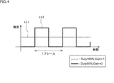
- FIG. 4 shows an example of luminance compensation at the time of black insertion drive.
- the horizontal axis represents time and the vertical axis represents brightness level.
- the waveform L11 shows the emission waveform of the OLED element during normal driving.
- the emission waveform of the normal drive always has a constant luminance level, indicates that the emission duty is 100% (Duty 100%) and the gain is 1 time (Gain ⁇ 1).
- Waveform L12 shows the light emission waveform of the OLED element when the black insertion is driven.
- the emission waveform of the black insertion drive is a rectangular wave, indicating that the emission duty is 50% (Duty 50%) and the gain is doubled (Gain ⁇ 2).
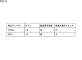
- FIG. 5 shows an example of the relationship between the light emission duty and gain, the moving image display performance, and the self-luminous element stress.
- a method of increasing the gain is used.
- the duty ratio is set to 100% and the gain is restored to minimize the temperature rise and stress of the LED etc., achieving both reliability and video performance. Further, in a fine image (a clear image frame having a high frequency component), a control for lowering the duty ratio is performed in order to enhance the effect of improving hold blur.
- the OLED display device has an OLED element as a self-luminous element, it is possible to control the light emission duty and improve the hold blur by changing the configuration of the drive circuit inside the display cell and performing black insertion drive. As mentioned earlier, it has become possible.
- the light emission duty is controlled according to parameters such as the amount of movement indicating the movement of the displayed object and the level of detail indicating the fineness of the image.
- the optimum duty value calculation unit 105 calculates the optimum light emission duty value using the amount of motion detected by the motion detection unit 103, thereby holding blurring the moving image. Make improvements in place.
- FIG. 6 shows an example of controlling the light emission duty according to the amount of movement.
- the horizontal axis represents the amount of motion (Motion)
- the vertical axis represents the light emission duty value.
- FIG. 6 it is shown that the movement amount of the displayed object in the image increases as the value on the horizontal axis moves to the right side, and the light emission duty value increases as the value on the vertical axis moves upward. Since hold blur is easily visible in an image including a display object having a large amount of movement, control is performed to reduce the light emission duty as shown by a polygonal line L21. On the other hand, in an image having a small amount of movement such as a still image, control is performed to increase the light emission duty as shown by the polygonal line L21. That is, the light emission duty value is lowered as the detected amount of movement increases.
- the optimum duty value calculation unit 105 calculates the optimum emission duty value using the detail level detected by the image flatness detection unit 101, so that the frequency component is high and clear. The hold blur is improved for the video (image frame including the edge).
- FIG. 7 shows an example of controlling the emission duty according to the level of detail.
- the horizontal axis represents the detail level (Detail_Lev), and the vertical axis represents the light emission duty value.
- FIG. 7 it is shown that the more the value on the horizontal axis goes to the right side, the finer the image includes more edge portions and the like, and the more the value on the vertical axis goes to the upper side, the higher the light emission duty value.
- control is performed to reduce the light emission duty as shown by the polygonal line L22.
- control is performed to increase the light emission duty as shown by the polygonal line L22. That is, the emission duty value decreases as the detected level of detail increases.
- the hold blur can be improved. Further, the stress of the OLED element can be reduced, and the decrease in the life of the OLED element can be suppressed.
- each pixel has a sub-pixel R that generates red (R) light, a sub-pixel G that generates green (G) light, a sub-pixel B that generates blue (B) light, and a white (W). It is composed of four sub-pixels of sub-pixel W that generate the light of.
- each pixel arranged two-dimensionally is an RGBW pixel.
- each pixel in the display area of the OLED display panel is RGBW pixel, but when lit at 100% level, the sub pixel R, the sub pixel G, and the sub pixel G are compared with the sub pixel W.
- the sub-pixel B has lower light emission efficiency and a larger current because it passes through a color filter corresponding to the wavelength band of each color. Therefore, the upper limit of the gain of the sub-pixel R, the sub-pixel G, and the sub-pixel B is lower than the gain of the sub-pixel W.
- complementary colors such as yellow (Y), magenta (M), and cyan (C) illuminate two sub-pixels in each pixel, so if they are lit at the maximum level as they are, the current limit value will be exceeded. It ends up.
- This current limit value depends on the temperature rise of the panel due to the self-heating of the OLED element and the limitation of the current capacity of the power supply.
- each pixel when the sub pixel R and the sub pixel G are lit, the color becomes yellow (Y), and when the sub pixel R and the sub pixel B are lit, the color becomes magenta (M), and the sub pixel G and the sub pixel B are displayed. When is lit, it becomes cyan (C).
- FIG. 8 shows an example of comparison of the drive current of the OLED element at the time of displaying each color.
- the horizontal axis represents the colors of the sub-pixels (W, R, G, B) and the colors (Y, M, C) when the sub-pixels are lit in two colors
- the vertical axis represents the EVDD current value. Shown.
- the EVDD current represents the total current flowing through the OLED element over the entire display area of the OLED display panel.
- the upper limit of the gain is lower.
- complementary colors such as yellow (Y), magenta (M), and cyan (C) exceed the current limit values shown by the broken lines in the figure when lit at the maximum level.
- the thick lines D1 to D3 the brightness level of the entire display area of the OLED display panel is lowered so as to be kept within the current limit value.
- the brightness of the sub-pixel W at the time of driving with black insertion for which brightness compensation is performed can be matched with the brightness at the time of driving without black insertion.
- the luminance level is the luminance of the input level 100%
- the luminance level of the sub-pixels R, G, and B is, for convenience, the luminance at the time of driving without black insertion as the luminance level of the sub-pixel W. It is said to be the same.
- the sub-pixel W can double the gain to compensate for the brightness, but the sub-pixels R, G, and B have an upper limit in gain, so the display area.
- the brightness level is lowered by lowering the light emission duty.
- FIG. 9 shows an example of peak brightness control at the time of black insertion drive for performing brightness compensation.
- the horizontal axis represents the average pixel level (APL) and the vertical axis represents the luminance level.
- the polygonal line L31 shows the control of the peak luminance of the sub-pixel W. Further, the polygonal lines L32 and L33 indicate the control of the peak luminance of the sub-pixels R, G, and B.
- the brightness level is lowered by setting the emission duty to 75% (Duty75%) in the region where the average pixel level is low. Can be avoided. In the region where the average pixel level is high, the emission duty is 50% (Duty50%) and 75% (Duty75%), which are almost the same brightness levels.
- the sub-pixels R, G, and B have a restriction that the upper limit value of the gain is lower than that of the sub-pixel W, the saturation of the highly saturated pixel is maintained even if the emission duty is lowered. Therefore, there is a problem that the gain cannot be raised sufficiently and the brightness is lowered. Therefore, in the present technology, in order to maintain the brightness balance between the low-saturation pixel and the high-saturation pixel, the lower limit value of the light emission duty is set according to the saturation level parameter.
- the optimum duty value calculation unit 105 calculates the optimum emission duty value using the saturation level detected by the saturation detection unit 102, so that the saturation is high. Make sure that the brightness balance between the low part and the low part is maintained.
- FIG. 10 shows an example of controlling the emission duty according to the saturation level.
- the horizontal axis represents the saturation level (Color_Sat_Lev), and the vertical axis represents the emission duty value.
- FIG. 10 it is shown that the more the value on the horizontal axis goes to the right, the higher the saturation becomes, and the more the value on the vertical axis goes to the upper side, the higher the emission duty value. If the emission duty is lowered for a large number of images, the brightness balance will be lost due to the upper limit of the gain of the sub-pixels R, G, and B. Therefore, as shown by the polygonal line L23, a lower limit value of the light emission duty is set according to the saturation level, and in an image having many high saturation regions, the light emission duty is controlled to be increased to obtain a pixel with high saturation. Ensure that the brightness balance of low pixels is maintained.
- Black crushing is a state in which the difference in brightness of a dark part cannot be sufficiently expressed and is filled like a solid black color.
- FIG. 11 shows an example of the gamma characteristic at the time of black insertion drive.
- the horizontal axis represents the input level and the vertical axis represents the output level.
- the straight line L41 indicates the target gamma value (2.2).
- the polygonal line L42 indicates a normal drive in which the light emission duty is 100% (Duty 100%) and the gain is 1 times (Gain ⁇ 1).
- the polygonal line L43 indicates a black insertion drive in which the light emission duty is 50% (Duty 50%) and the gain is doubled (Gain ⁇ 2).
- FIG. 12 shows an example of the effective light emission period during the normal drive and the black insertion drive.
- the horizontal axis represents time and the vertical axis represents voltage level.
- FIG. 12A shows the voltage fluctuation of the OLED element during normal driving, and the time after the voltage level indicated by the waveform L51 exceeds the threshold voltage Vth for each frame is the effective light emission period T1.
- FIG. 12B shows the voltage fluctuation of the OLED element during the black insertion drive, and the time after the voltage level indicated by the waveform L52 for each frame exceeds the threshold voltage Vth is the effective light emission period T2.
- the effective light emitting period T2 during the black insertion drive is shorter than the effective light emitting period T1 during the normal drive.
- the OLED element when the OLED element is driven with black insertion, the lower the gradation level, the greater the effect on the drive duty due to the rising characteristics of light emission. Therefore, when performing black insertion drive as a measure against hold blur, the light emission duty is set. As the value is lowered, the effective light emission period in the low gradation region is reduced, the brightness is significantly reduced, and black crushing tends to occur.
- the optimum duty value calculation unit 105 calculates the optimum emission duty value using the average pixel level (APL) detected by the APL detection unit 104, thereby lowering the order. Suppression of brightness reduction at the tuning level is implemented.
- APL average pixel level
- FIG. 13 shows an example of controlling the emission duty according to the average pixel level (APL).
- the horizontal axis represents the average pixel level (Ave_Pix_Lev), and the vertical axis represents the light emission duty value.
- Offset control In the above description, control of the emission duty according to the average pixel level (APL) has been described as a countermeasure for the decrease in brightness at a low gradation level when the OLED element is driven by inserting black, but other methods are used. It doesn't matter.
- the offset control unit 108 calculates an offset value related to the brightness of the video signal based on the light emission duty value calculated by the optimum duty value calculation unit 105, and adds the offset value to the video signal. May be performed so that the brightness is corrected.
- the offset value of the video signal By controlling the offset value of the video signal according to the light emission duty value in this way, the decrease in brightness at the low gradation level can be suppressed, and as a result, blackout can be suppressed.
- the gamma characteristic is corrected by correcting the brightness by the offset value.
- the OLED display panel is configured by arranging a plurality of OLED elements in a two-dimensional manner, a scan for a black signal is required to turn off each OLED element.
- the black insertion drive is performed, the light emitting region changes within one frame, and the current fluctuates.
- FIG. 14 shows an example of current fluctuation of the power supply circuit for driving the OLED element.
- the horizontal axis represents time and the vertical axis represents E VDD current value.
- the polygonal line L61 shows the temporal fluctuation of the EVDD current value. Further, in FIG. 14, the images I1 to I6 in one frame are arranged in time series, and correspond to the temporal fluctuation of the EVDD current value indicated by the polygonal line L61.
- the straight line L62 indicates a peak current limit value, and is controlled so that the peak current does not exceed this limit value. Further, the straight line L63 indicates an average current limit value, and is controlled so that the average current does not exceed this limit value.
- Image I is an image consisting of a monochromatic window represented by a dot pattern and a black background.
- the black insertion drive is performed, the light emitting region corresponding to the monochromatic window in the image I changes within one image frame as in the images I1 to I6.
- the EVDD current value indicated by the polygonal line L61 fluctuates according to this light emitting region.
- the frame FR on the image I indicates an area in which a black signal for black insertion is displayed in the frame.
- images I1 to I6 since the black insertion is performed from the upper side to the lower side, the scan proceeds downward and the displayed signal is updated from the upper side. That is, the black insertion area in the frame FR moves downward.
- the peak current increases by the average current ⁇ the gain, so that the EVDD current value indicated by the broken line L61 exceeds the peak current limit value.
- the E VDD current value is set to approximately 0.
- the average current of one frame can be set to the same value as when the black insertion drive is not performed, but since the light emitting region changes within one frame, the current There is a problem that there is fluctuation and it must be suppressed within the peak current value that the drive power supply circuit can tolerate. Therefore, in the present technology, the calculation method of the current limit is corrected according to the gain for luminance compensation, and the control is performed so that the peak current becomes a certain value or less.
- the calculated value of the peak current is corrected according to the gain, and even in the case where the peak current in which the load is concentrated is the maximum, the peak current limit value is not exceeded, for example, the peak current limit value is exceeded. It is possible to control the average current value to decrease according to the gain ratio.
- the peak current control unit 107 controls the peak current based on the gain calculated by the gain calculation unit 106 to limit the peak current to the peak current of the drive power supply circuit. Try to keep it within the value.
- FIG. 15 shows an example of peak current control.
- the horizontal axis represents time and the vertical axis represents E VDD current value.
- the polygonal line L71 shows the temporal fluctuation of the E VDD current value when the peak current control is not performed.
- the polygonal line L72 shows the temporal variation of the EVDD current value when the peak current is controlled.
- the straight line L73 indicates the peak current limit value. Further, the straight line L74 indicates an average current limit value.
- the limits regarding the current value in the drive power supply circuit include the limit of the average current value and the limit of the peak current value. If the peak current is not limited, the peak current value increases by a maximum of 1 / Duty. In the end (for example, in the case of Duty 50%, it is up to twice), and the peak current limit value is exceeded.
- the gain increased by the luminance compensation at the time of black insertion drive is controlled so as to be a value represented by the following equation (1).
- the peak current exceeds the peak current limit value L73 as shown by the polygonal line L71, but by performing the peak current control, it is shown by the polygonal line L72. , The peak current is controlled within the peak current limit value L73. As a result, the reliability of the drive power supply circuit can be ensured.
- FIG. 16 shows an example of the configuration of an embodiment of a self-luminous display device to which the present technology is applied.
- the self-luminous display device 1 is configured as a television receiver or the like.
- the self-luminous display device 1 includes a signal input unit 111, a signal processing unit 112, a display panel drive unit 113, and a self-luminous display panel 114.
- the signal processing unit 112 corresponds to the signal processing device 10 of FIG. 1
- the display panel driving unit 113 corresponds to the panel driver 20 of FIG.
- the signal input unit 111 is composed of a tuner connected to an antenna, a communication module that can be connected to a communication network such as the Internet, an input interface conforming to a predetermined standard, and the like.
- the signal input unit 111 records broadcast content transmitted by terrestrial broadcasting, satellite broadcasting, etc., communication content streamed via a communication network such as the Internet, or a recording medium such as an optical disk or semiconductor memory, a recorder, or the like. Video signals of various contents such as recorded contents are supplied to the signal processing unit 112.
- the signal processing unit 112 performs predetermined video signal processing based on the video signal of the content supplied from the signal input unit 111.
- a video signal and a control signal for controlling the drive of the self-luminous display panel 114 are generated and supplied to the display panel drive unit 113.
- the control signal includes parameters such as emission duty value (Duty), gain (Gain), current limit value (Cur_ratio), or offset value (offset).
- the display panel drive unit 113 drives the self-luminous display panel 114 based on the video signal and the control signal supplied from the signal processing unit 112.
- the self-luminous display panel 114 is a display panel in which pixels including self-luminous elements are arranged in a two-dimensional manner, and displays an image according to the drive from the display panel driving unit 113.
- the self-luminous display panel 114 an OLED display panel using an OLED element as the self-luminous element can be adopted.
- the self-luminous display device 1 is an OLED display device.
- the minimum configuration is shown for the sake of simplification of the description, but there are other devices such as an audio signal processing circuit that processes an audio signal and a speaker that outputs an audio according to the audio signal. Circuits and devices may be included.
- the optimum duty value calculation unit 105 calculates the light emission duty value
- one of the four parameters (Detail_Lev, Color_Sat_Lev, Motion, Ave_Pix_Lev) is of course used, and a plurality of parameters are used.
- the emission duty value may be calculated using the parameters of.
- the plurality of controls described above, for example, current control by the peak current control unit 107 and offset value control by the offset calculation unit 108 may be performed at the same time.
- the self-luminous display device 1 is a television receiver
- examples of the electronic device using the self-luminous display device 1 include a display device, a personal computer, and a tablet computer. It may be a smartphone, a mobile phone, a digital camera, a head mount display, a game machine, or the like.
- the self-luminous display device 1 may be used as a display unit for in-vehicle devices such as car navigation systems and rear seat monitors, or wearable devices such as wristwatch type and eyeglass type.
- the display device includes, for example, a medical monitor, a broadcasting monitor, a display for digital signage, and the like.
- OLED may be read as “organic EL”.
- the OLED display device can be said to be an organic EL display device.
- hold blur is also referred to as motion blur
- hold blur may be read as “movement blur”.
- video since the video is composed of a plurality of image frames, "video” may be read as "image”.
- a detector that analyzes the video signal of the content and detects an index that correlates with hold blur, A first calculation unit that calculates the light emission duty value of the self-luminous display panel based on the detected index, and A signal processing device including a second calculation unit that calculates a gain for luminance compensation based on the calculated emission duty value.
- the detection unit detects the amount of movement of the object displayed on the self-luminous display panel, and detects the amount of movement of the object.
- the signal processing device according to (1), wherein the first calculation unit calculates the light emission duty value according to the detected movement amount.
- the first calculation unit lowers the light emission duty value as the detected movement amount increases.
- the detection unit detects the level of detail of the image displayed on the self-luminous display panel.
- the signal processing device according to any one of (1) to (3), wherein the first calculation unit calculates the light emission duty value according to the detected detailed level.
- the first calculation unit lowers the emission duty value as the detected level of detail increases.
- the signal processing device according to (4), wherein the second calculation unit raises the gain in response to a change in the light emission duty value.
- the detection unit detects the saturation level of the image displayed on the self-luminous display panel.
- the signal processing device according to any one of (1) to (5), wherein the first calculation unit calculates the emission duty value according to the detected saturation level.
- the signal processing device according to (6), wherein the first calculation unit sets a limit on the lower limit of the emission duty value according to the detected saturation level.
- the detection unit detects the average pixel level of the video signal and The signal processing device according to any one of (1) to (7), wherein the first calculation unit calculates the light emission duty value according to the detected average pixel level.
- the first calculation unit sets a limit on the lower limit of the emission duty value, and increases the emission duty value as the average pixel level decreases.
- the signal processing device according to (8).
- the control unit (1) to (9) further includes a control unit that controls the current flowing through the self-luminous element arranged in the self-luminous display panel according to the gain so as to be suppressed within an allowable peak current by the power supply circuit. ).
- the signal processing device according to any one of. (11)
- the control unit controls so that the light emitting region of the self-luminous display panel does not exceed the peak current limit value when the peak current becomes maximum when the current fluctuation occurs due to a change within one frame of the image.
- (12) The signal processing device according to (11) above, wherein the control unit controls the gain to be a value obtained by dividing a peak current limit value by an average current limit value.
- the signal processing device according to any one of (1) to (12), further comprising a third calculation unit for calculating an offset value relating to the brightness of the video signal according to the light emission duty value.
- the signal processing apparatus according to (13), wherein the offset value corrects a decrease in brightness at a low gradation level.
- the signal processing device according to any one of (1) to (14) above, wherein the light emission duty is reduced by a black insertion drive provided with a black display period during the display period for displaying the same image.
- the gain is obtained by the reciprocal of the light emission duty value.
- the self-luminous display panel has a first sub-pixel that generates red (R) light, a second sub-pixel that generates green (G) light, and a third sub that generates blue (B) light.
- the signal processing apparatus according to any one of (1) to (16) above, wherein the pixels and the pixels having the fourth sub-pixels that generate white (W) light are arranged in a two-dimensional manner.
- the pixel includes an OLED (Organic Light Emitting Diode) element as a self-luminous element.
- the signal processing device Analyze the video signal of the content to detect the index that correlates with the hold blur, Based on the detected index, the light emission duty value of the self-luminous display panel is calculated.
- a signal processing method for calculating a gain for luminance compensation based on the calculated emission duty value (20) A signal processing unit that processes the video signal of the content, A self-luminous display panel that displays the video of the content, and A display panel drive unit that drives the self-luminous display panel based on a video signal from the signal processing unit is provided.
- the signal processing unit A detection unit that analyzes the video signal of the content and detects an index that correlates with hold blur.
- a first calculation unit that calculates the light emission duty value of the self-luminous display panel based on the detected index, and It has a second calculation unit that calculates the gain for luminance compensation based on the calculated emission duty value.
- the display panel drive unit is a display device that drives the self-luminous display panel based on the light emission duty value and the gain calculated by the signal processing unit.
- 1 Self-luminous display device 10 signal processing device, 20 panel driver, 30 signal line, 40 control line, 100 detection unit, 101 image flatness detection unit, 102 saturation detection unit, 103 motion detection unit, 104 APL detection unit , 105 Optimal duty value calculation unit, 106 Gain calculation unit, 107 Peak current control unit, 108 Offset calculation unit, 111 Signal input unit, 112 Signal processing unit, 113 Display panel drive unit, 114 Self-luminous display panel
Abstract
本技術は、より適切に、ホールドボケを改善することができるようにする信号処理装置、信号処理方法、及び表示装置に関する。 コンテンツの映像信号を解析して、ホールドボケに相関のある指標を検出する検出部と、検出した指標に基づいて、自発光表示パネルの発光デューティ値を算出する第1の算出部と、算出した発光デューティ値に基づいて、輝度補償のためのゲインを算出する第2の算出部とを備える信号処理装置が提供される。本技術は、例えば、自発光型表示装置に適用することができる。
Description
本技術は、信号処理装置、信号処理方法、及び表示装置に関し、特に、より適切に、ホールドボケを改善することができるようにした信号処理装置、信号処理方法、及び表示装置に関する。
近年、映像を表示する表示デバイスとして主流になりつつあるOLED表示装置は、ホールド型の表示装置である。この種の表示装置では、人間の視覚特性から、ホールドボケが発生することが報告されている。
この種のホールドボケの改善方法としては、各種の提案がなされている。例えば、映像コンテンツに含まれる物体の動きなどに応じて、液晶表示パネルに対して設けられるバックライトの駆動を制御することで、ホールドボケを改善する液晶表示装置が提案されている(特許文献1参照)。
ところで、OLED表示装置等の自発光型表示装置においても、ホールドボケを改善することが求められるが、現状では、そのような技術方式は確立されていない。
本技術はこのような状況に鑑みてなされたものであり、より適切に、ホールドボケを改善することができるようにするものである。
本技術の一側面の信号処理装置は、コンテンツの映像信号を解析して、ホールドボケに相関のある指標を検出する検出部と、検出した前記指標に基づいて、自発光表示パネルの発光デューティ値を算出する第1の算出部と、算出した前記発光デューティ値に基づいて、輝度補償のためのゲインを算出する第2の算出部とを備える信号処理装置である。
本技術の一側面の信号処理方法は、信号処理装置が、コンテンツの映像信号を解析して、ホールドボケに相関のある指標を検出し、検出した前記指標に基づいて、自発光表示パネルの発光デューティ値を算出し、算出した前記発光デューティ値に基づいて、輝度補償のためのゲインを算出する信号処理方法である。
本技術の一側面の表示装置は、コンテンツの映像信号を処理する信号処理部と、前記コンテンツの映像を表示する自発光表示パネルと、前記信号処理部からの映像信号に基づいて、前記自発光表示パネルを駆動する表示パネル駆動部とを備え、前記信号処理部は、前記コンテンツの映像信号を解析して、ホールドボケに相関のある指標を検出する検出部と、検出した前記指標に基づいて、前記自発光表示パネルの発光デューティ値を算出する第1の算出部と、算出した前記発光デューティ値に基づいて、輝度補償のためのゲインを算出する第2の算出部とを有し、前記表示パネル駆動部は、前記信号処理部により算出された前記発光デューティ値と前記ゲインに基づいて、前記自発光表示パネルを駆動する表示装置である。
本技術の一側面の信号処理装置、信号処理方法、及び表示装置においては、コンテンツの映像信号を解析して、ホールドボケに相関のある指標が検出され、検出された前記指標に基づいて、自発光表示パネルの発光デューティ値が算出され、算出された前記発光デューティ値に基づいて、輝度補償のためのゲインが算出される。
なお、本技術の一側面の信号処理装置、又は表示装置は、独立した装置であってもよいし、1つの装置を構成している内部ブロックであってもよい。
<1.本技術の実施の形態>
(信号処理装置の構成)
図1は、本技術を適用した信号処理装置の一実施の形態の構成の例を示している。
図1は、本技術を適用した信号処理装置の一実施の形態の構成の例を示している。
図1には、前段に設けられた信号入力部(不図示)から入力される入力信号を処理する信号処理装置10と、後段に設けられたOLED表示パネル(不図示)を駆動するパネルドライバ20を図示している。信号処理装置10とパネルドライバ20とは、複数の信号線30と制御線40により接続される。
信号処理装置10は、信号線30を介して、映像信号をパネルドライバ20に出力する。また、信号処理装置10は、制御線40を介して、制御信号をパネルドライバ20に出力する。
信号処理装置10は、そこに入力される入力信号に基づいて、所定の信号処理を行う。この信号処理では、OLED表示パネルの駆動を制御するための映像信号が生成され、パネルドライバ20に供給される。
パネルドライバ20は、信号処理装置10から供給される映像信号に基づいて、後段のOLED表示パネルを駆動する。
OLED表示パネルは、OLED素子を含む画素を2次元状(行列状)に配置した表示パネルであり、パネルドライバ20からの駆動に従い、映像の表示を行う。OLED表示パネルは、自発光素子としてOLED素子を用いた自発光型の表示パネルの一例である。なお、自発光型の表示パネルを有する自発光型表示装置の詳細は、図16を参照して後述する。
OLED(Organic Light Emitting Diode)は、陰極と陽極との間に、有機発光材料を挟んだ構造からなる発光素子であって、OLED表示パネルに2次元状に配列される画素(表示画素)を構成している。この画素に含まれるOLED素子は、信号処理によって生成される駆動制御信号に従って駆動される。OLED表示パネルにおいて、各画素(表示画素)は、例えば、赤色(R),緑色(G),青色(B),白色(W)の4つのサブ画素により構成される。
図2は、図1の信号処理装置10の詳細な構成を示している。
図2において、信号処理装置10は、画像平坦度検出部101、彩度検出部102、動き検出部103、APL検出部104、最適デューティ値算出部105、ゲイン算出部106、ピーク電流制御部107、及びオフセット算出部108から構成される。
画像平坦度検出部101は、そこに入力される映像信号に対する画像平坦度検出処理を行い、その処理の結果得られる詳細レベル(Detail_Lev)を、最適デューティ値算出部105に供給する。
例えば、ホールドボケは、エッジを多く含んだ細かい部分を含む画像フレームで発生し、平坦な部分では発生しないため、画像平坦度検出処理では、映像を構成する複数の画像フレームの空間解像度などを解析することで、映像信号に含まれるエッジ部分を表す指標として詳細レベルを検出する。この詳細レベルの検出方法としては、例えば、特定の周波数のみを通すバンドパスフィルタを用いて検出することができる。
彩度検出部102は、そこに入力される映像信号に対する彩度検出処理を行い、その処理の結果得られる彩度レベル(Color_Sat_Lev)を、最適デューティ値算出部105に供給する。
例えば、彩度検出処理では、映像信号から得られる色信号等を解析することで、映像の鮮やかさに関する特性を表す指標として彩度レベルを検出する。
動き検出部103は、そこに入力される映像信号に対する動き検出処理を行い、その処理の結果得られる動き量(Motion)を、最適デューティ値算出部105に供給する。
例えば、ホールドボケは、映像として表示される物体(表示物)が動いていないと発生しないため、動き検出処理では、映像内の表示物の動きを表す指標として動き量を検出する。この動き量の検出方法としては、例えば、画像フレーム間の各画素の輝度差分や、表示物の動きベクトル量を用いて検出することができる。
APL検出部104は、そこに入力される映像信号に対するAPL検出処理を行い、その処理の結果得られる平均画素レベル(Ave_Pix_Lev)を、最適デューティ値算出部105に供給する。
例えば、APL検出処理では、映像を構成する画像フレームの画素レベルの平均値を求めることで、映像に関する特性を表す指標として、平均画素レベルを検出する。
このように、画像平坦度検出部101、彩度検出部102、動き検出部103、及びAPL検出部104は、コンテンツの映像信号を解析して、ホールドボケに相関のある指標として各種のパラメータを検出する検出部100を構成している。そして、検出部100により検出される4つのパラメータ(Detail_Lev,Color_Sat_Lev,Motion,Ave_Pix_Lev)のうち、少なくとも1つのパラメータが、最適デューティ値算出部105に供給される。
なお、検出部100の処理対象となった映像信号は、信号線30を介してパネルドライバ20に出力される。
最適デューティ値算出部105は、検出部100から供給されるパラメータに基づいて、最適な発光デューティ値(Duty)を算出し、パネルドライバ20(図1)、ゲイン算出部106、又はオフセット算出部108に供給する。この発光デューティ値は、OLED表示パネルに配置されたOLED素子の発光のデューティ比であり、以下、発光デューティとも称する。
ゲイン算出部106は、最適デューティ値算出部105から供給される発光デューティ値に基づいて、輝度補償のためのゲイン(Gain)を算出し、パネルドライバ20、又はピーク電流制御部107に供給する。
ピーク電流制御部107は、ゲイン算出部106から供給されるゲインに基づいて、電流の制限値(Cur_ratio)を算出し、パネルドライバ20に供給する。
オフセット算出部108は、最適デューティ値算出部105から供給される発光デューティ値に基づいて、映像信号の輝度に関するオフセット値(offset)を算出し、パネルドライバ20に供給する。
パネルドライバ20には、発光デューティ値(Duty)、ゲイン(Gain)、電流の制限値(Cur_ratio)、及びオフセット値(offset)の4つのパラメータのうち、少なくとも1つのパラメータを含む制御信号が、制御線40を介して信号処理装置10から入力される。パネルドライバ20は、制御信号に含まれるパラメータに基づき、後段のOLED表示パネルを駆動する。
信号処理装置10は、以上のように構成される。
(黒挿入駆動の例)
ところで、OLED表示装置等の自発光型表示装置は、液晶表示装置等の非自発光型表示装置と同様に、ホールド型の表示装置である。ホールド型の表示装置では、原理的には、表示部に2次元状に配置された画素が、1フレーム間で、同一の輝度での表示(ホールド型表示)を行う。そのため、この種の表示装置では、人間の視覚特性から、ホールドボケが発生することが知られている。
ところで、OLED表示装置等の自発光型表示装置は、液晶表示装置等の非自発光型表示装置と同様に、ホールド型の表示装置である。ホールド型の表示装置では、原理的には、表示部に2次元状に配置された画素が、1フレーム間で、同一の輝度での表示(ホールド型表示)を行う。そのため、この種の表示装置では、人間の視覚特性から、ホールドボケが発生することが知られている。
例えば、OLED表示装置では、1フレーム期間点灯し続けた場合に、そのフレーム内の動く表示物をユーザが目で追ったときに、ホールド型の残像として感じることになる。OLED素子の発光デューティを小さくすれば、ホールドボケは改善するが、輝度を維持するためには、発光デューティ値の逆数(1/Duty)だけゲインを上げる必要がある。
図3は、黒挿入駆動によるホールドボケの改善の例を示している。図3のA,Bは、通常駆動時の実動作と視覚効果を示し、図3のC,Dは、黒挿入駆動時の実動作と視覚効果を示している。
通常駆動では、発光デューティが100%(Duty100%)での駆動を行う。一方で、黒挿入駆動では、同じ映像(画像フレーム)を表示する表示期間中に黒表示期間を設けることで、その映像の表示時間を短くしている。この黒挿入駆動により、動画表示性能を高くすることができる。黒挿入駆動では、発光デューティをDuty50%からDuty100%までの範囲で変化させることができ、この例では、発光デューティが50%(Duty50%)での駆動を行う場合を説明する。
図3において、時間の方向は、左側から右側に向かう方向とされ、0,1/240sec,2/240sec,3/240sec,4/240secの間に、画像フレームF1,F2,F3が順に表示される。
図3のAに示した通常駆動の実動作が行われた場合、図3のBの通常駆動の視覚効果に示すように、ユーザは、画像フレームF内の動く表示物(ボール)を目で追ったとき、ホールド型の残像を感じてしまう。
一方で、図3のCに示した黒挿入駆動が行われた場合、図3のDの黒挿入駆動の視覚効果に示すように、ホールドボケを改善することができる。しかしながら、発光デューティを小さくした場合、それに応じて輝度が低下してしまう。
図4は、黒挿入駆動時の輝度補償の例を示している。図4において、横軸は時間を示し、縦軸は輝度レベルを示している。
図4において、波形L11は、通常駆動時のOLED素子の発光波形を示している。通常駆動の発光波形は、常に一定の輝度レベルであり、発光デューティが100%(Duty100%)で、かつ、ゲインが1倍(Gain×1)であることを表している。
波形L12は、黒挿入駆動時のOLED素子の発光波形を示している。黒挿入駆動の発光波形は、矩形波となり、発光デューティが50%(Duty50%)で、かつ、ゲインが2倍(Gain×2)であることを表している。
このように、黒挿入駆動時に、Duty50%となる場合には、OLED素子の発光時の輝度が2倍になるようにゲインを上げて、平均輝度がDuty100%と同じになるようにすることで、輝度補償が行われる。
(動きやエッジに応じた制御)
図5は、発光デューティ及びゲインと、動画表示性能及び自発光素子ストレスとの関係の例を示している。
図5は、発光デューティ及びゲインと、動画表示性能及び自発光素子ストレスとの関係の例を示している。
図5に示すように、輝度を一定に保つために、発光デューティを50%に下げるときに、ゲインを2倍に上げることで、動画表示性能を向上させることはできるが、OLED素子等の自発光素子のストレスが増大してしまう。そのため、静止画では、発光デューティを100%に戻して、OLED素子のストレスを軽減させて、OLED素子の寿命の低下を抑制する必要がある。
例えば、液晶表示装置では、ホールド型のホールドボケを改善するために、動きの速い表示物を含む画像フレームでは、LED(Light Emitting Diode)等のバックライトを点灯させるデューティ比を下げて、輝度補償のために、ゲインを上げる手法が用いられている。
一方で、静止画の画像フレームでは、デューティ比を100%に、ゲインを元に戻してLED等の温度上昇やストレスを最小限に抑えて、信頼性と動画性能を両立させている。また、細かい映像(周波数成分の高いはっきりとした画像フレーム)では、ホールドボケの改善効果を高めるために、デューティ比を下げる制御が行われている。
OLED表示装置では、自発光素子としてのOLED素子を有するため、表示セル内部の駆動回路の構成に変更を加えて黒挿入駆動を行うことで、発光デューティを制御し、ホールドボケを改善することが可能になったのは、先に述べた通りである。
OLED表示装置において、黒挿入駆動時の輝度低下を抑えるために、ゲインをかけて輝度補償することは可能であるが、常時この駆動を行うと、OLED素子へのストレスが増加し、寿命が低下してしまう。そこで、本技術では、表示物の動きを示す動き量や、映像の細かさを示す詳細レベルなどのパラメータに応じて、発光デューティが制御されるようにしている。
具体的には、信号処理装置10において、最適デューティ値算出部105が、動き検出部103により検出された動き量を用いて、最適な発光デューティ値を算出することで、動画に対してホールドボケの改善が実施されるようにする。
図6は、動き量に応じた発光デューティの制御の例を示している。図6において、横軸は動き量(Motion)を示し、縦軸は発光デューティ値を示している。
図6においては、横軸の値が右側にいくほど、映像内の表示物の動き量が大きくなり、縦軸の値が上側に行くほど、発光デューティ値が高くなることを示しているが、動き量が大きい表示物を含む映像では、ホールドボケが視認されやすいため、折れ線L21で示すように、発光デューティを下げる制御を行う。一方で、静止画などの動き量が小さい映像では、折れ線L21で示すように、発光デューティを上げる制御が行われる。すなわち、検出された動き量の増加とともに発光デューティ値が下げられる。
また、信号処理装置10において、最適デューティ値算出部105が、画像平坦度検出部101により検出された詳細レベルを用いて、最適な発光デューティ値を算出することで、周波数成分の高いはっきりとした映像(エッジを含む画像フレーム)に対してホールドボケの改善が実施されるようにする。
図7は、詳細レベルに応じた発光デューティの制御の例を示している。図7において、横軸は詳細レベル(Detail_Lev)を示し、縦軸は発光デューティ値を示している。
図7においては、横軸の値が右側にいくほど、より多くのエッジ部分等を含む細かい映像であることを示し、縦軸の値が上側に行くほど、発光デューティ値が高くなることを示しているが、細かい映像では、ホールドボケが視認されやすいため、折れ線L22で示すように、発光デューティを下げる制御を行う。一方で、平坦な映像では、折れ線L22で示すように、発光デューティを上げる制御が行われる。すなわち、検出された詳細レベルの増加とともに発光デューティ値が下げられる。
このような発光デューティの制御が実施されることで、ホールドボケを改善することができる。また、OLED素子のストレスを軽減させて、OLED素子の寿命の低下を抑制することができる。
(彩度に応じた制御)
OLED表示装置では、OLED表示パネルの表示領域に、複数の画素が2次元状に配列される。各画素は、赤色(R)の光を発生するサブ画素Rと、緑色(G)の光を発生するサブ画素Gと、青色(B)の光を発生するサブ画素Bと、白色(W)の光を発生するサブ画素Wの4つのサブ画素から構成される。換言すれば、OLED表示パネルの表示領域において、2次元状に配列される各画素は、RGBW画素とされる。
OLED表示装置では、OLED表示パネルの表示領域に、複数の画素が2次元状に配列される。各画素は、赤色(R)の光を発生するサブ画素Rと、緑色(G)の光を発生するサブ画素Gと、青色(B)の光を発生するサブ画素Bと、白色(W)の光を発生するサブ画素Wの4つのサブ画素から構成される。換言すれば、OLED表示パネルの表示領域において、2次元状に配列される各画素は、RGBW画素とされる。
ここで、OLED表示パネルの表示領域の各画素の構成は、RGBW画素となるが、100%のレベルで点灯させた際には、サブ画素Wに比べて、サブ画素R、サブ画素G、及びサブ画素Bのほうが、各色の波長帯に応じたカラーフィルタを通す都合上発光効率が悪く、電流が多くなる。このため、サブ画素R、サブ画素G、及びサブ画素Bのゲインの上限値は、サブ画素Wのゲインよりも低くなる。
また、黄色(Y)、マゼンタ色(M)、及びシアン色(C)のような補色は、各画素におけるサブ画素を2色点灯させるため、そのまま最大レベルで点灯した場合、電流制限値を超えてしまう。
そのため、OLED表示パネルの表示領域全体の輝度レベルを落として、電流制限値内に抑える必要がある。この電流制限値は、OLED素子の自己発熱によるパネルの温度上昇や電源の電流容量の制約に依存するものである。
なお、各画素において、サブ画素Rとサブ画素Gが点灯すると、黄色(Y)になり、サブ画素Rとサブ画素Bが点灯すると、マゼンタ色(M)になり、サブ画素Gとサブ画素Bが点灯すると、シアン色(C)になる。
図8は、各色表示時のOLED素子の駆動電流の比較の例を示している。図8において、横軸は、サブ画素の色(W,R,G,B)と、サブ画素を2色点灯した時の色(Y,M,C)を示し、縦軸はEVDD電流値を示している。EVDD電流は、OLED表示パネルの表示領域全体のOLED素子に流れる電流の合計を表している。
図8に示すように、サブ画素R、サブ画素G、及びサブ画素Bは、サブ画素Wに比べて、EVDD電流値が高いため、ゲインの上限値が低くなる。また、黄色(Y)、マゼンタ色(M)、及びシアン色(C)のような補色は、最大レベルで点灯した場合、図中の破線で示した電流制限値を超えてしまうため、図中の太線D1乃至D3で示すように、OLED表示パネルの表示領域全体の輝度レベルを落として、電流制限値内に抑えるようにする。
ここで、輝度補償を行う黒挿入駆動時のサブ画素Wの輝度は、黒挿入なし駆動時の輝度と一致させることができる。ただし、このとき、輝度レベルは、入力レベル100%の輝度であり、サブ画素R,G,Bの輝度レベルは、便宜的に、黒挿入なし駆動時の輝度を、サブ画素Wの輝度レベルと同じであるとしている。
例えば、黒挿入駆動時にDuty50%の場合、サブ画素Wは、ゲインを2倍にして輝度補償が可能であるが、サブ画素R,G,Bについては、ゲインに上限値があるため、表示領域のうち、平均画素レベル(APL:Average Pixel Level)の低い領域では、発光デューティを下げていくことで、輝度レベルが下がってしまう。
図9は、輝度補償を行う黒挿入駆動時におけるピーク輝度制御の例を示している。図9において、横軸は平均画素レベル(APL)を示し、縦軸は輝度レベルを示している。
図9において、折れ線L31は、サブ画素Wのピーク輝度の制御を示している。また、折れ線L32,L33は、サブ画素R,G,Bのピーク輝度の制御を示している。
図9に示すように、サブ画素R,G,Bは、ゲインに上限値があるため、平均画素レベルが低い領域では、発光デューティを75%(Duty75%)とすることで、輝度レベルが下がらないようにすることができる。なお、平均画素レベルが高い領域では、発光デューティが50%(Duty50%)と75%(Duty75%)で、ほぼ同程度の輝度レベルとされる。
このように、サブ画素R,G,Bは、サブ画素Wと比べて、ゲインの上限値が低いという制約があるため、彩度の高い画素では、発光デューティを下げても、彩度を維持するために、ゲインを十分に上げられずに、輝度が低下してしまうという問題がある。そこで、本技術では、彩度の低い画素と高い画素の輝度バランスを維持するために、彩度レベルのパラメータに応じて、発光デューティの下限値を設定するようにしている。
具体的には、信号処理装置10において、最適デューティ値算出部105が、彩度検出部102により検出された彩度レベルを用いて、最適な発光デューティ値を算出することで、彩度が高い部分と低い部分の輝度バランスが保たれるようにする。
図10は、彩度レベルに応じた発光デューティの制御の例を示している。図10において、横軸は彩度レベル(Color_Sat_Lev)を示し、縦軸は発光デューティ値を示している。
図10においては、横軸の値が右側にいくほど、彩度が高くなり、縦軸の値が上側に行くほど、発光デューティ値が高くなることを示しているが、彩度が高い領域が多い映像で発光デューティを下げてしまうと、サブ画素R,G,Bのゲインの上限制約により輝度バランスが崩れてしまう。そのため、折れ線L23で示すように、彩度レベルに応じて発光デューティの下限値を設けて、彩度の高い領域が多い映像では、発光デューティを上げる制御を行うことで、彩度が高い画素と低い画素の輝度バランスの維持が実施されるようにする。
(APLに応じた制御)
OLED表示パネルにおいて、OLED素子の両端に電圧をかけてから、発光量が所定の量に達するまでに要する時間は、低い階調レベルになるほど、駆動デューティに対する影響が大きくなる。
OLED表示パネルにおいて、OLED素子の両端に電圧をかけてから、発光量が所定の量に達するまでに要する時間は、低い階調レベルになるほど、駆動デューティに対する影響が大きくなる。
そのため、OLED表示装置が、ホールドボケ対策として黒挿入駆動を行う際に、発光デューティを下げるにしたがって、低階調領域での実効発光期間が減少し、黒潰れが生じる傾向にある。黒潰れとは、暗い部分の明るさ差分が十分に表現できず、黒一色のように塗りつぶされた状態である。
図11は、黒挿入駆動時のガンマ特性の例を示している。図11において、横軸が入力レベルを示し、縦軸が出力レベルを示している。
図11において、直線L41は、目標となるガンマ値(2.2)を示している。折れ線L42は、発光デューティが100%(Duty100%)であって、ゲインが1倍(Gain×1)である通常駆動を示している。折れ線L43は、発光デューティが50%(Duty50%)であって、ゲインが2倍(Gain×2)である黒挿入駆動を示している。
図11の左下の領域における直線L41と、折れ線L42,L43との関係に注目すれば、OLED素子を駆動した場合に、発光の立ち上がり特性により、低い階調レベルほど、駆動デューティに対する影響が大きくなることは明らかである。
図12は、通常駆動時と黒挿入駆動時における実効発光期間の例を示している。図12において、横軸が時間を示し、縦軸が電圧レベルを示している。
図12のAは、通常駆動時のOLED素子の電圧変動を示しており、1フレームごとに波形L51で示す電圧レベルが閾値電圧Vthを超えてからの時間が、実効発光期間T1となる。図12のBは、黒挿入駆動時のOLED素子の電圧変動を示しており、1フレームごとに波形L52で示す電圧レベルが閾値電圧Vthを超えてからの時間が、実効発光期間T2となる。黒挿入駆動時の実効発光期間T2は、通常駆動時の実効発光期間T1よりも期間が短くなる。
このように、OLED素子を黒挿入駆動時した場合、発光の立ち上がり特性により、低い階調レベルほど、駆動デューティに対する影響が大きくなるため、ホールドボケ対策として黒挿入駆動を行う際に、発光デューティを下げるにしたがって、低階調領域での実効発光期間が減少して輝度低下が顕著になり、黒潰れが生じる傾向にある。
そこで、本技術では、平均画素レベル(APL)の低い画像フレーム(画面全体が暗い映像)の場合には、ホールドボケの改善効果があまり感じられないことに注目して、平均画素レベルのパラメータに応じて発光デューティの下限値を制御することで、ガンマ特性のずれを抑えて、低階調レベルでの黒潰れを抑制するようにしている。
具体的には、信号処理装置10において、最適デューティ値算出部105が、APL検出部104により検出された平均画素レベル(APL)を用いて、最適な発光デューティ値を算出することで、低階調レベルでの輝度低下の抑制が実施されるようにする。
図13は、平均画素レベル(APL)に応じた発光デューティの制御の例を示している。図13において、横軸は平均画素レベル(Ave_Pix_Lev)を示し、縦軸は発光デューティ値を示している。
図13においては、横軸の値が右側にいくほど、平均画素レベルが高く明るい映像であることを示し、縦軸の値が上側に行くほど、発光デューティ値が高くなることを示しているが、平均画素レベルが低い暗い映像では、発光デューティを下げてしまうと、黒潰れしてしまう傾向がある。そのため、折れ線L24で示すように、平均画素レベルに応じて発光デューティの下限値を設けて、平均画素レベルが低いときには、発光デューティを上げる制御を行い、平均画素レベルの減少とともに発光デューティ値が上げられようにすることで、低階調レベルでの黒潰れの抑制が実施されるようにする。
(オフセット制御)
上述した説明では、OLED素子を黒挿入駆動した場合の低階調レベルでの輝度低下の対策として、平均画素レベル(APL)に応じた発光デューティの制御を説明したが、他の手法を用いても構わない。
上述した説明では、OLED素子を黒挿入駆動した場合の低階調レベルでの輝度低下の対策として、平均画素レベル(APL)に応じた発光デューティの制御を説明したが、他の手法を用いても構わない。
例えば、信号処理装置10において、オフセット制御部108が、最適デューティ値算出部105により算出された発光デューティ値に基づき、映像信号の輝度に関するオフセット値を算出し、当該オフセット値を映像信号に加える制御を行うことで、輝度が補正されるようにしてもよい。
このように、発光デューティ値に応じて映像信号のオフセット値を制御することで、低階調レベルの輝度低下が抑制され、結果として黒潰れを抑制することができる。なお、ここでは、オフセット値によって輝度を補正することで、ガンマ特性を補正していると捉えることもできる。
(ピーク電流制御)
OLED表示パネルは、複数のOLED素子が2次元状に配置されて構成されるため、各OLED素子を消灯するためには、黒信号用のスキャンが必要となる。黒挿入駆動を行う場合には、発光領域が1フレーム内で変化して、電流が変動することになる。
OLED表示パネルは、複数のOLED素子が2次元状に配置されて構成されるため、各OLED素子を消灯するためには、黒信号用のスキャンが必要となる。黒挿入駆動を行う場合には、発光領域が1フレーム内で変化して、電流が変動することになる。
そのため、あるスキャンタイミングで負荷が集中するような表示の場合、ピーク電流が、平均電流×ゲイン分だけ増加してしまい、OLED素子の駆動用電源回路のピーク電流制限値を超えてしまうという問題がある。
図14は、OLED素子の駆動用電源回路の電流変動の例を示している。図14において、横軸は時間を示し、縦軸はEVDD電流値を示している。
図14において、折れ線L61は、EVDD電流値の時間的な変動を示している。また、図14では、1フレーム内の画像I1乃至I6が、時系列に並べられており、折れ線L61により示されるEVDD電流値の時間的な変動に対応している。
なお、直線L62は、ピーク電流制限値を示し、この制限値をピーク電流が超えないように制御される。また、直線L63は、平均電流制限値を示し、この制限値を平均電流が超えないように制御される。
画像Iは、ドットパターンで表した単色ウィンドウと、黒色の背景からなる画像である。黒挿入駆動を行う場合、画像Iにおける単色ウィンドウに対応した発光領域が、画像I1乃至I6のように1つの画像フレーム内で変化する。このとき、この発光領域に対応して、折れ線L61により示したEVDD電流値が変動する。
また、図14において、画像I上の枠FRは、その枠内に黒挿入用の黒信号が表示された領域を示している。画像I1乃至I6で表現されるように、黒挿入は上側から下側に向かって行われるため、下方向にスキャンが進行し、上側から、表示される信号が更新される。つまり、枠FR内の黒挿入の領域が下方向に移動していくことになる。
ここで、1フレーム内の画像I1,I2,I6などのように、ドットパターンの横帯で表した発光領域がある程度の高さを有するとき、すなわち、あるスキャンタイミングで負荷が集中するような表示となる場合、ピーク電流は、平均電流×ゲイン分だけ増加することで、折れ線L61で示すEVDD電流値が、ピーク電流制限値を超えてしまう。
なお、1フレーム内の画像I4などのように、発光領域が存在しない場合には、EVDD電流値は略0とされる。
このように、黒挿入駆動を行う場合でも、1フレームの平均電流は、黒挿入駆動を行わない場合と同一の値にすることができるが、1フレーム内で発光する領域が変化するため、電流変動があり、駆動用電源回路が許容できるピーク電流値以内に抑えなければならないという問題がある。そこで、本技術では、輝度補償のためのゲインに応じて電流制限の算出方法を補正し、ピーク電流が一定値以下になるように制御が行われるようにしている。
すなわち、本技術では、ゲインに応じて、ピーク電流の算出値を補正し、負荷が集中したピーク電流が最大のケースでも、ピーク電流制限値を超えないように、例えば、ピーク電流制限値を超えたゲインの比率に応じて平均電流値が下がるような制御を行うことができる。
具体的には、信号処理装置10において、ピーク電流制御部107が、ゲイン算出部106により算出されたゲインに基づき、ピーク電流を制御することで、ピーク電流を、駆動用電源回路のピーク電流制限値内に抑えるようにする。
図15は、ピーク電流制御の例を示している。図15において、横軸は時間を示し、縦軸はEVDD電流値を示している。
図15において、折れ線L71は、ピーク電流制御を行わない場合のEVDD電流値の時間的な変動を示している。折れ線L72は、ピーク電流制御を行う場合のEVDD電流値の時間的な変動を示している。なお、直線L73は、ピーク電流制限値を示している。また、直線L74は、平均電流制限値を示している。
ここで、駆動用電源回路における電流値に関する制限には、平均電流値の制限と、ピーク電流値の制限があり、ピーク電流を制限しない場合、ピーク電流値は、最大1/Dutyだけ増加してしまい(例えば、Duty50%の場合には最大2倍)、ピーク電流制限値を超えてしまう。
ピーク電流を、ピーク電流制限値内に抑えるためには、表示領域全体のゲインを下げる制御が必要になる。図15に示した例では、黒挿入駆動時の輝度補償で上げるゲインを、下記の式(1)で表すような値になるように制御している。
ゲイン = ピーク電流制限値 / 平均電流制限値 ・・・(1)
このように、ピーク電流制御を行わない場合には、折れ線L71で示すように、ピーク電流が、ピーク電流制限値L73を超えていたが、ピーク電流制御を行うことで、折れ線L72で示すように、ピーク電流が、ピーク電流制限値L73内に制御される。これにより、駆動用電源回路の信頼性を担保することができる。
(自発光型表示装置の構成)
図16は、本技術を適用した自発光型表示装置の一実施の形態の構成の例を示している。
図16は、本技術を適用した自発光型表示装置の一実施の形態の構成の例を示している。
図16において、自発光型表示装置1は、テレビ受像機などとして構成される。自発光型表示装置1は、信号入力部111、信号処理部112、表示パネル駆動部113、及び自発光表示パネル114から構成される。なお、信号処理部112は、図1の信号処理装置10に対応し、表示パネル駆動部113は、図1のパネルドライバ20に対応している。
信号入力部111は、アンテナに接続されたチューナ、インターネット等の通信網に接続可能な通信モジュール、又は所定の規格に準拠した入力インターフェースなどから構成される。
信号入力部111は、地上波放送や衛星放送などにより送信される放送コンテンツ、インターネット等の通信網を介してストリーミング配信される通信コンテンツ、又は光ディスクや半導体メモリ等の記録媒体や録画機などに記録された記録コンテンツなどの各種のコンテンツの映像信号を、信号処理部112に供給する。
信号処理部112は、信号入力部111から供給されるコンテンツの映像信号に基づいて、所定の映像信号処理を行う。この映像信号処理では、自発光表示パネル114の駆動を制御するための映像信号と制御信号が生成され、表示パネル駆動部113に供給される。例えば、制御信号は、発光デューティ値(Duty)、ゲイン(Gain)、電流の制限値(Cur_ratio)、又はオフセット値(offset)等のパラメータを含む。
表示パネル駆動部113は、信号処理部112から供給される映像信号と制御信号に基づいて、自発光表示パネル114を駆動する。自発光表示パネル114は、自発光素子を含む画素を2次元状に配置した表示パネルであり、表示パネル駆動部113からの駆動に従い、映像の表示を行う。
自発光表示パネル114としては、自発光素子としてOLED素子を用いたOLED表示パネルを採用することができる。自発光表示パネル114として、OLED表示パネルを採用した場合、自発光型表示装置1は、OLED表示装置とされる。
なお、図16に示した構成では、説明の簡略化のため、最小限の構成を示したが、音声信号を処理する音声信号処理回路や、音声信号に応じた音声を出力するスピーカなど、他の回路やデバイス等を含めても構わない。
<2.変形例>
信号処理装置10において、最適デューティ値算出部105によって、発光デューティ値を算出する際には、4つのパラメータ(Detail_Lev,Color_Sat_Lev,Motion,Ave_Pix_Lev)のうち、1つのパラメータを使用することは勿論、複数のパラメータを用い、発光デューティ値を算出しても構わない。また、信号処理装置10においては、上述した複数の制御、例えば、ピーク電流制御部107による電流制御と、オフセット算出部108によるオフセット値制御などが同時に実施されても構わない。
上述した説明では、自発光型表示装置1が、テレビ受像機である場合を例示したが、自発光型表示装置1を用いた電子機器としては、例えば、ディスプレイ装置、パーソナルコンピュータ、タブレット型コンピュータ、スマートフォン、携帯電話機、デジタルカメラ、ヘッドマウントディスプレイ、ゲーム機などであってもよい。
さらには、自発光型表示装置1を、カーナビゲーションや後部座席用モニタ等の車載機器、又は腕時計型や眼鏡型等のウェアラブル機器などの表示部として用いても構わない。なお、ディスプレイ装置としては、例えば、メディカル用のモニタや放送用モニタ、デジタルサイネージ用のディスプレイなどを含む。
なお、本明細書において、「OLED」は、「有機EL」と読み替えても構わない。例えば、OLED表示装置は、有機EL表示装置であるとも言える。また、ホールドボケは、動きボケとも称されるため、「ホールドボケ」を、「動きボケ」と読み替えても構わない。さらに、映像は、複数の画像フレームから構成されるものであるため、「映像」を、「画像」と読み替えても構わない。
なお、本技術の実施の形態は、上述した実施の形態に限定されるものではなく、本技術の要旨を逸脱しない範囲において種々の変更が可能である。
また、本明細書に記載された効果はあくまで例示であって限定されるものではなく、他の効果があってもよい。
なお、本技術は、以下のような構成をとることができる。
(1)
コンテンツの映像信号を解析して、ホールドボケに相関のある指標を検出する検出部と、
検出した前記指標に基づいて、自発光表示パネルの発光デューティ値を算出する第1の算出部と、
算出した前記発光デューティ値に基づいて、輝度補償のためのゲインを算出する第2の算出部と
を備える信号処理装置。
(2)
前記検出部は、前記自発光表示パネルに表示される物体の動き量を検出し、
前記第1の算出部は、検出した前記動き量に応じた前記発光デューティ値を算出する
前記(1)に記載の信号処理装置。
(3)
前記第1の算出部は、検出した前記動き量の増加とともに、前記発光デューティ値を下げ、
前記第2の算出部は、前記発光デューティ値の変化に応じて、前記ゲインを上げる
前記(2)に記載の信号処理装置。
(4)
前記検出部は、前記自発光表示パネルに表示される映像の詳細レベルを検出し、
前記第1の算出部は、検出した前記詳細レベルに応じた前記発光デューティ値を算出する
前記(1)乃至(3)のいずれかに記載の信号処理装置。
(5)
前記第1の算出部は、検出した前記詳細レベルの増加とともに、前記発光デューティ値を下げ、
前記第2の算出部は、前記発光デューティ値の変化に応じて、前記ゲインを上げる
前記(4)に記載の信号処理装置。
(6)
前記検出部は、前記自発光表示パネルに表示される映像の彩度レベルを検出し、
前記第1の算出部は、検出した前記彩度レベルに応じた前記発光デューティ値を算出する
前記(1)乃至(5)のいずれかに記載の信号処理装置。
(7)
前記第1の算出部は、検出した前記彩度レベルに応じて、前記発光デューティ値の下限値の制限を設ける
前記(6)に記載の信号処理装置。
(8)
前記検出部は、前記映像信号の平均画素レベルを検出し、
前記第1の算出部は、検出した前記平均画素レベルに応じた前記発光デューティ値を算出する
前記(1)乃至(7)のいずれかに記載の信号処理装置。
(9)
前記第1の算出部は、検出した前記平均画素レベルが一定レベル未満となる場合、前記発光デューティ値の下限値の制限を設けて、前記平均画素レベルの減少とともに、前記発光デューティ値を上げる
前記(8)に記載の信号処理装置。
(10)
前記ゲインに応じて、前記自発光表示パネルに配置された自発光素子に流れる電流を、電源回路が許容可能なピーク電流内に抑えるように制御する制御部をさらに備える
前記(1)乃至(9)のいずれかに記載の信号処理装置。
(11)
前記制御部は、前記自発光表示パネルの発光領域が、映像の1フレーム内で変化して電流変動が生じたとき、ピーク電流が最大となる場合にピーク電流制限値を超えないように制御する
前記(10)に記載の信号処理装置。
(12)
前記制御部は、前記ゲインが、ピーク電流制限値を平均電流制限値で除算した値になるように制御する
前記(11)に記載の信号処理装置。
(13)
前記発光デューティ値に応じて、前記映像信号の輝度に関するオフセット値を算出する第3の算出部をさらに備える
前記(1)乃至(12)のいずれかに記載の信号処理装置。
(14)
前記オフセット値により低階調レベルでの輝度の低下が補正される
前記(13)に記載の信号処理装置。
(15)
同じ映像を表示する表示期間中に黒表示期間を設けた黒挿入駆動により、発光デューティを小さくする
前記(1)乃至(14)のいずれかに記載の信号処理装置。
(16)
前記ゲインは、前記発光デューティ値の逆数により求められる
前記(15)に記載の信号処理装置。
(17)
前記自発光表示パネルは、赤色(R)の光を発生する第1のサブ画素、緑色(G)の光を発生する第2のサブ画素、青色(B)の光を発生する第3のサブ画素、及び白色(W)の光を発生する第4のサブ画素を有する画素を2次元状に配置している
前記(1)乃至(16)のいずれかに記載の信号処理装置。
(18)
前記画素は、自発光素子としてOLED(Organic Light Emitting Diode)素子を含んで構成される
前記(17)に記載の信号処理装置。
(19)
信号処理装置が、
コンテンツの映像信号を解析して、ホールドボケに相関のある指標を検出し、
検出した前記指標に基づいて、自発光表示パネルの発光デューティ値を算出し、
算出した前記発光デューティ値に基づいて、輝度補償のためのゲインを算出する
信号処理方法。
(20)
コンテンツの映像信号を処理する信号処理部と、
前記コンテンツの映像を表示する自発光表示パネルと、
前記信号処理部からの映像信号に基づいて、前記自発光表示パネルを駆動する表示パネル駆動部と
を備え、
前記信号処理部は、
前記コンテンツの映像信号を解析して、ホールドボケに相関のある指標を検出する検出部と、
検出した前記指標に基づいて、前記自発光表示パネルの発光デューティ値を算出する第1の算出部と、
算出した前記発光デューティ値に基づいて、輝度補償のためのゲインを算出する第2の算出部と
を有し、
前記表示パネル駆動部は、前記信号処理部により算出された前記発光デューティ値と前記ゲインに基づいて、前記自発光表示パネルを駆動する
表示装置。
1 自発光型表示装置, 10 信号処理装置, 20 パネルドライバ, 30 信号線, 40 制御線, 100 検出部, 101 画像平坦度検出部, 102 彩度検出部, 103 動き検出部, 104 APL検出部, 105 最適デューティ値算出部, 106 ゲイン算出部, 107 ピーク電流制御部, 108 オフセット算出部, 111 信号入力部, 112 信号処理部, 113 表示パネル駆動部, 114 自発光表示パネル
Claims (20)
- コンテンツの映像信号を解析して、ホールドボケに相関のある指標を検出する検出部と、
検出した前記指標に基づいて、自発光表示パネルの発光デューティ値を算出する第1の算出部と、
算出した前記発光デューティ値に基づいて、輝度補償のためのゲインを算出する第2の算出部と
を備える信号処理装置。 - 前記検出部は、前記自発光表示パネルに表示される物体の動き量を検出し、
前記第1の算出部は、検出した前記動き量に応じた前記発光デューティ値を算出する
請求項1に記載の信号処理装置。 - 前記第1の算出部は、検出した前記動き量の増加とともに、前記発光デューティ値を下げ、
前記第2の算出部は、前記発光デューティ値の変化に応じて、前記ゲインを上げる
請求項2に記載の信号処理装置。 - 前記検出部は、前記自発光表示パネルに表示される映像の詳細レベルを検出し、
前記第1の算出部は、検出した前記詳細レベルに応じた前記発光デューティ値を算出する
請求項1に記載の信号処理装置。 - 前記第1の算出部は、検出した前記詳細レベルの増加とともに、前記発光デューティ値を下げ、
前記第2の算出部は、前記発光デューティ値の変化に応じて、前記ゲインを上げる
請求項4に記載の信号処理装置。 - 前記検出部は、前記自発光表示パネルに表示される映像の彩度レベルを検出し、
前記第1の算出部は、検出した前記彩度レベルに応じた前記発光デューティ値を算出する
請求項1に記載の信号処理装置。 - 前記第1の算出部は、検出した前記彩度レベルに応じて、前記発光デューティ値の下限値の制限を設ける
請求項6に記載の信号処理装置。 - 前記検出部は、前記映像信号の平均画素レベルを検出し、
前記第1の算出部は、検出した前記平均画素レベルに応じた前記発光デューティ値を算出する
請求項1に記載の信号処理装置。 - 前記第1の算出部は、検出した前記平均画素レベルが一定レベル未満となる場合、前記発光デューティ値の下限値の制限を設けて、前記平均画素レベルの減少とともに、前記発光デューティ値を上げる
請求項8に記載の信号処理装置。 - 前記ゲインに応じて、前記自発光表示パネルに配置された自発光素子に流れる電流を、電源回路が許容可能なピーク電流内に抑えるように制御する制御部をさらに備える
請求項1に記載の信号処理装置。 - 前記制御部は、前記自発光表示パネルの発光領域が、映像の1フレーム内で変化して電流変動が生じたとき、ピーク電流が最大となる場合にピーク電流制限値を超えないように制御する
請求項10に記載の信号処理装置。 - 前記制御部は、前記ゲインが、ピーク電流制限値を平均電流制限値で除算した値になるように制御する
請求項11に記載の信号処理装置。 - 前記発光デューティ値に応じて、前記映像信号の輝度に関するオフセット値を算出する第3の算出部をさらに備える
請求項1に記載の信号処理装置。 - 前記オフセット値により低階調レベルでの輝度の低下が補正される
請求項13に記載の信号処理装置。 - 同じ映像を表示する表示期間中に黒表示期間を設けた黒挿入駆動により、発光デューティを小さくする
請求項1に記載の信号処理装置。 - 前記ゲインは、前記発光デューティ値の逆数により求められる
請求項15に記載の信号処理装置。 - 前記自発光表示パネルは、赤色(R)の光を発生する第1のサブ画素、緑色(G)の光を発生する第2のサブ画素、青色(B)の光を発生する第3のサブ画素、及び白色(W)の光を発生する第4のサブ画素を有する画素を2次元状に配置している
請求項1に記載の信号処理装置。 - 前記画素は、自発光素子としてOLED(Organic Light Emitting Diode)素子を含んで構成される
請求項17に記載の信号処理装置。 - 信号処理装置が、
コンテンツの映像信号を解析して、ホールドボケに相関のある指標を検出し、
検出した前記指標に基づいて、自発光表示パネルの発光デューティ値を算出し、
算出した前記発光デューティ値に基づいて、輝度補償のためのゲインを算出する
信号処理方法。 - コンテンツの映像信号を処理する信号処理部と、
前記コンテンツの映像を表示する自発光表示パネルと、
前記信号処理部からの映像信号に基づいて、前記自発光表示パネルを駆動する表示パネル駆動部と
を備え、
前記信号処理部は、
前記コンテンツの映像信号を解析して、ホールドボケに相関のある指標を検出する検出部と、
検出した前記指標に基づいて、前記自発光表示パネルの発光デューティ値を算出する第1の算出部と、
算出した前記発光デューティ値に基づいて、輝度補償のためのゲインを算出する第2の算出部と
を有し、
前記表示パネル駆動部は、前記信号処理部により算出された前記発光デューティ値と前記ゲインに基づいて、前記自発光表示パネルを駆動する
表示装置。
Priority Applications (4)
| Application Number | Priority Date | Filing Date | Title |
|---|---|---|---|
| US17/757,768 US20230018404A1 (en) | 2019-12-27 | 2020-12-14 | Signal processing device, signal processing method, and display device |
| EP20905180.4A EP4083983A4 (en) | 2019-12-27 | 2020-12-14 | SIGNAL PROCESSING DEVICE, SIGNAL PROCESSING METHOD AND DISPLAY DEVICE |
| CN202080088009.6A CN114846534A (zh) | 2019-12-27 | 2020-12-14 | 信号处理装置、信号处理方法以及显示装置 |
| JP2021567265A JPWO2021131830A1 (ja) | 2019-12-27 | 2020-12-14 |
Applications Claiming Priority (2)
| Application Number | Priority Date | Filing Date | Title |
|---|---|---|---|
| JP2019238105 | 2019-12-27 | ||
| JP2019-238105 | 2019-12-27 |
Publications (1)
| Publication Number | Publication Date |
|---|---|
| WO2021131830A1 true WO2021131830A1 (ja) | 2021-07-01 |
Family
ID=76574424
Family Applications (1)
| Application Number | Title | Priority Date | Filing Date |
|---|---|---|---|
| PCT/JP2020/046460 WO2021131830A1 (ja) | 2019-12-27 | 2020-12-14 | 信号処理装置、信号処理方法、及び表示装置 |
Country Status (5)
| Country | Link |
|---|---|
| US (1) | US20230018404A1 (ja) |
| EP (1) | EP4083983A4 (ja) |
| JP (1) | JPWO2021131830A1 (ja) |
| CN (1) | CN114846534A (ja) |
| WO (1) | WO2021131830A1 (ja) |
Families Citing this family (2)
| Publication number | Priority date | Publication date | Assignee | Title |
|---|---|---|---|---|
| KR20210129310A (ko) * | 2020-04-17 | 2021-10-28 | 삼성디스플레이 주식회사 | 표시 장치 및 그 구동 방법 |
| KR20220084602A (ko) * | 2020-12-14 | 2022-06-21 | 엘지디스플레이 주식회사 | 전계 발광 표시장치와 그 구동방법 |
Citations (8)
| Publication number | Priority date | Publication date | Assignee | Title |
|---|---|---|---|---|
| JP2004252216A (ja) * | 2003-02-20 | 2004-09-09 | Hitachi Ltd | 自発光型表示装置とその駆動方法 |
| JP2006189658A (ja) * | 2005-01-06 | 2006-07-20 | Toshiba Corp | 画像表示装置及びその画像表示方法 |
| JP2008139797A (ja) * | 2006-12-05 | 2008-06-19 | Semiconductor Energy Lab Co Ltd | 表示装置およびその駆動方法 |
| WO2008153055A1 (ja) * | 2007-06-13 | 2008-12-18 | Sony Corporation | 表示装置、映像信号処理方法、およびプログラム |
| JP2010160237A (ja) * | 2009-01-07 | 2010-07-22 | Seiko Epson Corp | 発光制御信号生成方法、発光制御信号生成回路、表示装置、電子機器 |
| US20160155382A1 (en) * | 2014-11-27 | 2016-06-02 | Samsung Display Co., Ltd. | Display device and method of driving the display device |
| JP2018151666A (ja) * | 2018-06-08 | 2018-09-27 | 双葉電子工業株式会社 | 表示駆動装置、表示装置、表示駆動方法 |
| WO2019124254A1 (ja) | 2017-12-19 | 2019-06-27 | ソニー株式会社 | 信号処理装置、信号処理方法、及び表示装置 |
Family Cites Families (6)
| Publication number | Priority date | Publication date | Assignee | Title |
|---|---|---|---|---|
| JP4433041B2 (ja) * | 2007-11-16 | 2010-03-17 | ソニー株式会社 | 表示装置、画像信号処理方法、およびプログラム |
| JP2010015008A (ja) * | 2008-07-04 | 2010-01-21 | Samsung Electronics Co Ltd | 映像信号処理装置、映像信号処理方法、プログラム、および表示装置 |
| TW201445542A (zh) * | 2013-05-20 | 2014-12-01 | Sony Corp | 影像信號處理電路、影像信號處理方法及顯示裝置 |
| CN105489170B (zh) * | 2014-09-16 | 2019-08-06 | 青岛海信电器股份有限公司 | 一种背光源的驱动方法、装置及显示设备 |
| US10497321B2 (en) * | 2017-10-31 | 2019-12-03 | Wuhan China Star Optoelectronics Technology Co., Ltd. | Image processing method and device thereof |
| CN109360530B (zh) * | 2018-10-30 | 2023-06-27 | 武汉华星光电技术有限公司 | 液晶显示装置及其背光控制方法 |
-
2020
- 2020-12-14 EP EP20905180.4A patent/EP4083983A4/en active Pending
- 2020-12-14 US US17/757,768 patent/US20230018404A1/en active Pending
- 2020-12-14 CN CN202080088009.6A patent/CN114846534A/zh active Pending
- 2020-12-14 JP JP2021567265A patent/JPWO2021131830A1/ja active Pending
- 2020-12-14 WO PCT/JP2020/046460 patent/WO2021131830A1/ja unknown
Patent Citations (8)
| Publication number | Priority date | Publication date | Assignee | Title |
|---|---|---|---|---|
| JP2004252216A (ja) * | 2003-02-20 | 2004-09-09 | Hitachi Ltd | 自発光型表示装置とその駆動方法 |
| JP2006189658A (ja) * | 2005-01-06 | 2006-07-20 | Toshiba Corp | 画像表示装置及びその画像表示方法 |
| JP2008139797A (ja) * | 2006-12-05 | 2008-06-19 | Semiconductor Energy Lab Co Ltd | 表示装置およびその駆動方法 |
| WO2008153055A1 (ja) * | 2007-06-13 | 2008-12-18 | Sony Corporation | 表示装置、映像信号処理方法、およびプログラム |
| JP2010160237A (ja) * | 2009-01-07 | 2010-07-22 | Seiko Epson Corp | 発光制御信号生成方法、発光制御信号生成回路、表示装置、電子機器 |
| US20160155382A1 (en) * | 2014-11-27 | 2016-06-02 | Samsung Display Co., Ltd. | Display device and method of driving the display device |
| WO2019124254A1 (ja) | 2017-12-19 | 2019-06-27 | ソニー株式会社 | 信号処理装置、信号処理方法、及び表示装置 |
| JP2018151666A (ja) * | 2018-06-08 | 2018-09-27 | 双葉電子工業株式会社 | 表示駆動装置、表示装置、表示駆動方法 |
Non-Patent Citations (1)
| Title |
|---|
| See also references of EP4083983A4 |
Also Published As
| Publication number | Publication date |
|---|---|
| CN114846534A (zh) | 2022-08-02 |
| US20230018404A1 (en) | 2023-01-19 |
| JPWO2021131830A1 (ja) | 2021-07-01 |
| EP4083983A1 (en) | 2022-11-02 |
| EP4083983A4 (en) | 2023-05-03 |
Similar Documents
| Publication | Publication Date | Title |
|---|---|---|
| EP3098803B1 (en) | Image processing method, image processing circuit, and organic light emitting diode display device using the same | |
| US8358293B2 (en) | Method for driving light source blocks, driving unit for performing the method and display apparatus having the driving unit | |
| RU2497168C2 (ru) | Жидкокристаллический дисплей | |
| US8593391B2 (en) | Liquid crystal display device control circuit and liquid crystal display system, which adjust brightness of display image by using height distribution of gradations of input image | |
| US9183797B2 (en) | Display device and control method for display device | |
| EP3223266B1 (en) | Organic light emitting diode display device and method of operating the same | |
| KR20100007748A (ko) | 표시 장치, 표시 장치의 구동 방법, 구동용 집적 회로, 구동용 집적 회로에 의한 구동 방법 및 신호 처리 방법 | |
| KR102385628B1 (ko) | 표시장치 및 그의 구동방법 | |
| US11942049B2 (en) | Signal processing apparatus, signal processing method, and display apparatus | |
| US20160140924A1 (en) | Data clipping method and display device using the same | |
| WO2021131830A1 (ja) | 信号処理装置、信号処理方法、及び表示装置 | |
| KR102510573B1 (ko) | 투명 표시 장치 및 그 구동 방법 | |
| KR20160035192A (ko) | 표시장치와 그 휘도 향상 방법 | |
| KR20150071549A (ko) | 표시 장치 및 이를 이용한 표시장치의 구동 방법 | |
| US20230410733A1 (en) | Signal Processing Apparatus, Signal Processing Method, And Display Apparatus | |
| JP2008176111A (ja) | 画像表示装置および画像表示方法 | |
| US20230162668A1 (en) | Signal Processing Device, Signal Processing Method, And Display Device | |
| KR101611907B1 (ko) | 표시 장치의 색 보정 방법 및 장치 | |
| KR101870991B1 (ko) | 표시 장치의 색 보정장치 및 방법 | |
| JP2013250562A (ja) | 表示装置、映像種別判定装置、表示装置の駆動方法、及び映像種別の判定方法 | |
| KR20140092159A (ko) | 표시 장치 및 그 구동 방법 |
Legal Events
| Date | Code | Title | Description |
|---|---|---|---|
| 121 | Ep: the epo has been informed by wipo that ep was designated in this application |
Ref document number: 20905180 Country of ref document: EP Kind code of ref document: A1 |
|
| ENP | Entry into the national phase |
Ref document number: 2021567265 Country of ref document: JP Kind code of ref document: A |
|
| NENP | Non-entry into the national phase |
Ref country code: DE |
|
| ENP | Entry into the national phase |
Ref document number: 2020905180 Country of ref document: EP Effective date: 20220727 |