WO2021131830A1 - Dispositif de traitement de signal, procédé de traitement de signal et dispositif d'affichage - Google Patents
Dispositif de traitement de signal, procédé de traitement de signal et dispositif d'affichage Download PDFInfo
- Publication number
- WO2021131830A1 WO2021131830A1 PCT/JP2020/046460 JP2020046460W WO2021131830A1 WO 2021131830 A1 WO2021131830 A1 WO 2021131830A1 JP 2020046460 W JP2020046460 W JP 2020046460W WO 2021131830 A1 WO2021131830 A1 WO 2021131830A1
- Authority
- WO
- WIPO (PCT)
- Prior art keywords
- signal processing
- emission duty
- light emission
- self
- duty value
- Prior art date
Links
Images


Classifications
-
- G—PHYSICS
- G09—EDUCATION; CRYPTOGRAPHY; DISPLAY; ADVERTISING; SEALS
- G09G—ARRANGEMENTS OR CIRCUITS FOR CONTROL OF INDICATING DEVICES USING STATIC MEANS TO PRESENT VARIABLE INFORMATION
- G09G3/00—Control arrangements or circuits, of interest only in connection with visual indicators other than cathode-ray tubes
- G09G3/20—Control arrangements or circuits, of interest only in connection with visual indicators other than cathode-ray tubes for presentation of an assembly of a number of characters, e.g. a page, by composing the assembly by combination of individual elements arranged in a matrix no fixed position being assigned to or needed to be assigned to the individual characters or partial characters
- G09G3/22—Control arrangements or circuits, of interest only in connection with visual indicators other than cathode-ray tubes for presentation of an assembly of a number of characters, e.g. a page, by composing the assembly by combination of individual elements arranged in a matrix no fixed position being assigned to or needed to be assigned to the individual characters or partial characters using controlled light sources
- G09G3/30—Control arrangements or circuits, of interest only in connection with visual indicators other than cathode-ray tubes for presentation of an assembly of a number of characters, e.g. a page, by composing the assembly by combination of individual elements arranged in a matrix no fixed position being assigned to or needed to be assigned to the individual characters or partial characters using controlled light sources using electroluminescent panels
- G09G3/32—Control arrangements or circuits, of interest only in connection with visual indicators other than cathode-ray tubes for presentation of an assembly of a number of characters, e.g. a page, by composing the assembly by combination of individual elements arranged in a matrix no fixed position being assigned to or needed to be assigned to the individual characters or partial characters using controlled light sources using electroluminescent panels semiconductive, e.g. using light-emitting diodes [LED]
- G09G3/3208—Control arrangements or circuits, of interest only in connection with visual indicators other than cathode-ray tubes for presentation of an assembly of a number of characters, e.g. a page, by composing the assembly by combination of individual elements arranged in a matrix no fixed position being assigned to or needed to be assigned to the individual characters or partial characters using controlled light sources using electroluminescent panels semiconductive, e.g. using light-emitting diodes [LED] organic, e.g. using organic light-emitting diodes [OLED]
-
- G—PHYSICS
- G09—EDUCATION; CRYPTOGRAPHY; DISPLAY; ADVERTISING; SEALS
- G09G—ARRANGEMENTS OR CIRCUITS FOR CONTROL OF INDICATING DEVICES USING STATIC MEANS TO PRESENT VARIABLE INFORMATION
- G09G3/00—Control arrangements or circuits, of interest only in connection with visual indicators other than cathode-ray tubes
- G09G3/20—Control arrangements or circuits, of interest only in connection with visual indicators other than cathode-ray tubes for presentation of an assembly of a number of characters, e.g. a page, by composing the assembly by combination of individual elements arranged in a matrix no fixed position being assigned to or needed to be assigned to the individual characters or partial characters
- G09G3/2007—Display of intermediate tones
- G09G3/2077—Display of intermediate tones by a combination of two or more gradation control methods
- G09G3/2081—Display of intermediate tones by a combination of two or more gradation control methods with combination of amplitude modulation and time modulation
-
- G—PHYSICS
- G09—EDUCATION; CRYPTOGRAPHY; DISPLAY; ADVERTISING; SEALS
- G09G—ARRANGEMENTS OR CIRCUITS FOR CONTROL OF INDICATING DEVICES USING STATIC MEANS TO PRESENT VARIABLE INFORMATION
- G09G3/00—Control arrangements or circuits, of interest only in connection with visual indicators other than cathode-ray tubes
- G09G3/20—Control arrangements or circuits, of interest only in connection with visual indicators other than cathode-ray tubes for presentation of an assembly of a number of characters, e.g. a page, by composing the assembly by combination of individual elements arranged in a matrix no fixed position being assigned to or needed to be assigned to the individual characters or partial characters
- G09G3/34—Control arrangements or circuits, of interest only in connection with visual indicators other than cathode-ray tubes for presentation of an assembly of a number of characters, e.g. a page, by composing the assembly by combination of individual elements arranged in a matrix no fixed position being assigned to or needed to be assigned to the individual characters or partial characters by control of light from an independent source
- G09G3/3406—Control of illumination source
- G09G3/342—Control of illumination source using several illumination sources separately controlled corresponding to different display panel areas, e.g. along one dimension such as lines
- G09G3/3426—Control of illumination source using several illumination sources separately controlled corresponding to different display panel areas, e.g. along one dimension such as lines the different display panel areas being distributed in two dimensions, e.g. matrix
-
- H—ELECTRICITY
- H10—SEMICONDUCTOR DEVICES; ELECTRIC SOLID-STATE DEVICES NOT OTHERWISE PROVIDED FOR
- H10K—ORGANIC ELECTRIC SOLID-STATE DEVICES
- H10K71/00—Manufacture or treatment specially adapted for the organic devices covered by this subclass
- H10K71/70—Testing, e.g. accelerated lifetime tests
-
- G—PHYSICS
- G09—EDUCATION; CRYPTOGRAPHY; DISPLAY; ADVERTISING; SEALS
- G09G—ARRANGEMENTS OR CIRCUITS FOR CONTROL OF INDICATING DEVICES USING STATIC MEANS TO PRESENT VARIABLE INFORMATION
- G09G2320/00—Control of display operating conditions
- G09G2320/02—Improving the quality of display appearance
- G09G2320/0223—Compensation for problems related to R-C delay and attenuation in electrodes of matrix panels, e.g. in gate electrodes or on-substrate video signal electrodes
-
- G—PHYSICS
- G09—EDUCATION; CRYPTOGRAPHY; DISPLAY; ADVERTISING; SEALS
- G09G—ARRANGEMENTS OR CIRCUITS FOR CONTROL OF INDICATING DEVICES USING STATIC MEANS TO PRESENT VARIABLE INFORMATION
- G09G2320/00—Control of display operating conditions
- G09G2320/02—Improving the quality of display appearance
- G09G2320/0233—Improving the luminance or brightness uniformity across the screen
-
- G—PHYSICS
- G09—EDUCATION; CRYPTOGRAPHY; DISPLAY; ADVERTISING; SEALS
- G09G—ARRANGEMENTS OR CIRCUITS FOR CONTROL OF INDICATING DEVICES USING STATIC MEANS TO PRESENT VARIABLE INFORMATION
- G09G2320/00—Control of display operating conditions
- G09G2320/02—Improving the quality of display appearance
- G09G2320/0238—Improving the black level
-
- G—PHYSICS
- G09—EDUCATION; CRYPTOGRAPHY; DISPLAY; ADVERTISING; SEALS
- G09G—ARRANGEMENTS OR CIRCUITS FOR CONTROL OF INDICATING DEVICES USING STATIC MEANS TO PRESENT VARIABLE INFORMATION
- G09G2320/00—Control of display operating conditions
- G09G2320/02—Improving the quality of display appearance
- G09G2320/0261—Improving the quality of display appearance in the context of movement of objects on the screen or movement of the observer relative to the screen
-
- G—PHYSICS
- G09—EDUCATION; CRYPTOGRAPHY; DISPLAY; ADVERTISING; SEALS
- G09G—ARRANGEMENTS OR CIRCUITS FOR CONTROL OF INDICATING DEVICES USING STATIC MEANS TO PRESENT VARIABLE INFORMATION
- G09G2320/00—Control of display operating conditions
- G09G2320/02—Improving the quality of display appearance
- G09G2320/0271—Adjustment of the gradation levels within the range of the gradation scale, e.g. by redistribution or clipping
-
- G—PHYSICS
- G09—EDUCATION; CRYPTOGRAPHY; DISPLAY; ADVERTISING; SEALS
- G09G—ARRANGEMENTS OR CIRCUITS FOR CONTROL OF INDICATING DEVICES USING STATIC MEANS TO PRESENT VARIABLE INFORMATION
- G09G2320/00—Control of display operating conditions
- G09G2320/02—Improving the quality of display appearance
- G09G2320/029—Improving the quality of display appearance by monitoring one or more pixels in the display panel, e.g. by monitoring a fixed reference pixel
-
- G—PHYSICS
- G09—EDUCATION; CRYPTOGRAPHY; DISPLAY; ADVERTISING; SEALS
- G09G—ARRANGEMENTS OR CIRCUITS FOR CONTROL OF INDICATING DEVICES USING STATIC MEANS TO PRESENT VARIABLE INFORMATION
- G09G2320/00—Control of display operating conditions
- G09G2320/04—Maintaining the quality of display appearance
- G09G2320/043—Preventing or counteracting the effects of ageing
- G09G2320/045—Compensation of drifts in the characteristics of light emitting or modulating elements
-
- G—PHYSICS
- G09—EDUCATION; CRYPTOGRAPHY; DISPLAY; ADVERTISING; SEALS
- G09G—ARRANGEMENTS OR CIRCUITS FOR CONTROL OF INDICATING DEVICES USING STATIC MEANS TO PRESENT VARIABLE INFORMATION
- G09G2320/00—Control of display operating conditions
- G09G2320/06—Adjustment of display parameters
- G09G2320/0626—Adjustment of display parameters for control of overall brightness
- G09G2320/064—Adjustment of display parameters for control of overall brightness by time modulation of the brightness of the illumination source
-
- G—PHYSICS
- G09—EDUCATION; CRYPTOGRAPHY; DISPLAY; ADVERTISING; SEALS
- G09G—ARRANGEMENTS OR CIRCUITS FOR CONTROL OF INDICATING DEVICES USING STATIC MEANS TO PRESENT VARIABLE INFORMATION
- G09G2320/00—Control of display operating conditions
- G09G2320/10—Special adaptations of display systems for operation with variable images
- G09G2320/103—Detection of image changes, e.g. determination of an index representative of the image change
-
- G—PHYSICS
- G09—EDUCATION; CRYPTOGRAPHY; DISPLAY; ADVERTISING; SEALS
- G09G—ARRANGEMENTS OR CIRCUITS FOR CONTROL OF INDICATING DEVICES USING STATIC MEANS TO PRESENT VARIABLE INFORMATION
- G09G2330/00—Aspects of power supply; Aspects of display protection and defect management
- G09G2330/02—Details of power systems and of start or stop of display operation
- G09G2330/021—Power management, e.g. power saving
-
- G—PHYSICS
- G09—EDUCATION; CRYPTOGRAPHY; DISPLAY; ADVERTISING; SEALS
- G09G—ARRANGEMENTS OR CIRCUITS FOR CONTROL OF INDICATING DEVICES USING STATIC MEANS TO PRESENT VARIABLE INFORMATION
- G09G2330/00—Aspects of power supply; Aspects of display protection and defect management
- G09G2330/04—Display protection
- G09G2330/045—Protection against panel overheating
-
- G—PHYSICS
- G09—EDUCATION; CRYPTOGRAPHY; DISPLAY; ADVERTISING; SEALS
- G09G—ARRANGEMENTS OR CIRCUITS FOR CONTROL OF INDICATING DEVICES USING STATIC MEANS TO PRESENT VARIABLE INFORMATION
- G09G2360/00—Aspects of the architecture of display systems
- G09G2360/14—Detecting light within display terminals, e.g. using a single or a plurality of photosensors
- G09G2360/145—Detecting light within display terminals, e.g. using a single or a plurality of photosensors the light originating from the display screen
- G09G2360/147—Detecting light within display terminals, e.g. using a single or a plurality of photosensors the light originating from the display screen the originated light output being determined for each pixel
-
- G—PHYSICS
- G09—EDUCATION; CRYPTOGRAPHY; DISPLAY; ADVERTISING; SEALS
- G09G—ARRANGEMENTS OR CIRCUITS FOR CONTROL OF INDICATING DEVICES USING STATIC MEANS TO PRESENT VARIABLE INFORMATION
- G09G2360/00—Aspects of the architecture of display systems
- G09G2360/16—Calculation or use of calculated indices related to luminance levels in display data
Definitions
- the present technology relates to a signal processing device, a signal processing method, and a display device, and more particularly to a signal processing device, a signal processing method, and a display device capable of improving hold blur more appropriately.
- OLED display devices which are becoming mainstream as display devices for displaying images, are hold-type display devices. It has been reported that hold blur occurs in this type of display device due to human visual characteristics.
- Patent Document 1 a liquid crystal display device that improves hold blur by controlling the drive of a backlight provided on a liquid crystal display panel according to the movement of an object included in the video content has been proposed.
- This technology was made in view of such a situation, and makes it possible to improve hold blur more appropriately.
- the signal processing device of one aspect of the present technology analyzes the video signal of the content, detects an index correlating with the hold blur, and the light emitting duty value of the self-luminous display panel based on the detected index.
- This is a signal processing device including a first calculation unit for calculating the brightness compensation and a second calculation unit for calculating the gain for luminance compensation based on the calculated emission duty value.
- the signal processing device analyzes the video signal of the content, detects an index correlating with the hold blur, and emits light from the self-luminous display panel based on the detected index.
- This is a signal processing method for calculating a duty value and calculating a gain for luminance compensation based on the calculated light emission duty value.
- the display device on one aspect of the present technology includes a signal processing unit that processes a video signal of the content, a self-luminous display panel that displays the video of the content, and the self-luminous light based on the video signal from the signal processing unit.
- a display panel driving unit for driving the display panel is provided, and the signal processing unit analyzes the video signal of the content to detect an index correlating with hold blur, and the signal processing unit is based on the detected index.
- the self-luminous display panel has a first calculation unit for calculating a light emission duty value and a second calculation unit for calculating a gain for brightness compensation based on the calculated light emission duty value.
- the display panel drive unit is a display device that drives the self-luminous display panel based on the light emission duty value and the gain calculated by the signal processing unit.
- the video signal of the content is analyzed, an index correlating with the hold blur is detected, and the self is based on the detected index.
- the light emission duty value of the light emission display panel is calculated, and the gain for luminance compensation is calculated based on the calculated light emission duty value.
- the signal processing device or display device on one side of the present technology may be an independent device or an internal block constituting one device.
- FIG. 1 shows an example of the configuration of an embodiment of a signal processing device to which the present technology is applied.
- FIG. 1 shows a signal processing device 10 for processing an input signal input from a signal input unit (not shown) provided in the front stage, and a panel driver 20 for driving an OLED display panel (not shown) provided in the rear stage. Is illustrated.
- the signal processing device 10 and the panel driver 20 are connected by a plurality of signal lines 30 and control lines 40.
- the signal processing device 10 outputs a video signal to the panel driver 20 via the signal line 30. Further, the signal processing device 10 outputs a control signal to the panel driver 20 via the control line 40.
- the signal processing device 10 performs predetermined signal processing based on the input signal input therein. In this signal processing, a video signal for controlling the drive of the OLED display panel is generated and supplied to the panel driver 20.
- the panel driver 20 drives the OLED display panel in the subsequent stage based on the video signal supplied from the signal processing device 10.
- the OLED display panel is a display panel in which pixels including OLED elements are arranged in a two-dimensional shape (matrix shape), and displays an image according to the drive from the panel driver 20.
- the OLED display panel is an example of a self-luminous display panel using an OLED element as a self-luminous element. The details of the self-luminous display device having the self-luminous display panel will be described later with reference to FIG.
- OLED Organic Light Emitting Diode
- OLED Organic Light Emitting Diode
- each pixel (display pixel) is composed of, for example, four sub-pixels of red (R), green (G), blue (B), and white (W).
- FIG. 2 shows a detailed configuration of the signal processing device 10 of FIG.
- the signal processing device 10 includes an image flatness detection unit 101, a saturation detection unit 102, a motion detection unit 103, an APL detection unit 104, an optimum duty value calculation unit 105, a gain calculation unit 106, and a peak current control unit 107. , And the offset calculation unit 108.
- the image flatness detection unit 101 performs image flatness detection processing on the video signal input therein, and supplies the detail level (Detail_Lev) obtained as a result of the processing to the optimum duty value calculation unit 105.
- the image flatness detection process the spatial resolution of a plurality of image frames constituting the image is analyzed. By doing so, the detail level is detected as an index representing the edge portion included in the video signal.
- a bandpass filter that passes only a specific frequency can be used for detection.
- the saturation detection unit 102 performs saturation detection processing on the video signal input therein, and supplies the saturation level (Color_Sat_Lev) obtained as a result of the processing to the optimum duty value calculation unit 105.
- the saturation level is detected as an index showing the characteristics related to the vividness of the image by analyzing the color signal or the like obtained from the image signal.
- the motion detection unit 103 performs motion detection processing on the video signal input therein, and supplies the motion amount (Motion) obtained as a result of the processing to the optimum duty value calculation unit 105.
- the amount of movement is detected as an index indicating the movement of the displayed object in the image.
- the difference in brightness of each pixel between image frames and the amount of motion vector of the displayed object can be used for detection.
- the APL detection unit 104 performs APL detection processing on the video signal input therein, and supplies the average pixel level (Ave_Pix_Lev) obtained as a result of the processing to the optimum duty value calculation unit 105.
- the average pixel level is detected as an index showing the characteristics related to the image by obtaining the average value of the pixel levels of the image frames constituting the image.
- the image flatness detection unit 101, the saturation detection unit 102, the motion detection unit 103, and the APL detection unit 104 analyze the video signal of the content and use various parameters as indexes correlating with the hold blur. It constitutes a detection unit 100 for detection. Then, at least one of the four parameters (Detail_Lev, Color_Sat_Lev, Motion, Ave_Pix_Lev) detected by the detection unit 100 is supplied to the optimum duty value calculation unit 105.
- the video signal processed by the detection unit 100 is output to the panel driver 20 via the signal line 30.
- the optimum duty value calculation unit 105 calculates the optimum light emission duty value (Duty) based on the parameters supplied from the detection unit 100, and the panel driver 20 (FIG. 1), the gain calculation unit 106, or the offset calculation unit 108. Supply to.
- This emission duty value is the emission duty ratio of the OLED element arranged on the OLED display panel, and is also hereinafter referred to as emission duty.
- the gain calculation unit 106 calculates the gain for luminance compensation based on the light emission duty value supplied from the optimum duty value calculation unit 105, and supplies the gain to the panel driver 20 or the peak current control unit 107.
- the peak current control unit 107 calculates a current limit value (Cur_ratio) based on the gain supplied from the gain calculation unit 106, and supplies the current limit value (Cur_ratio) to the panel driver 20.
- the offset calculation unit 108 calculates an offset value related to the brightness of the video signal based on the light emission duty value supplied from the optimum duty value calculation unit 105, and supplies the offset value (offset) to the panel driver 20.
- the panel driver 20 is controlled by a control signal including at least one of four parameters of emission duty value (Duty), gain (Gain), current limit value (Cur_ratio), and offset value (offset). It is input from the signal processing device 10 via the line 40.
- the panel driver 20 drives the OLED display panel in the subsequent stage based on the parameters included in the control signal.
- the signal processing device 10 is configured as described above.
- a self-luminous display device such as an OLED display device is a hold-type display device like a non-self-luminous display device such as a liquid crystal display device.
- the hold-type display device in principle, pixels arranged in a two-dimensional manner on the display unit perform display (hold-type display) with the same brightness between one frame. Therefore, it is known that hold blur occurs in this type of display device due to human visual characteristics.
- an OLED display device when a moving display object in the frame is continuously lit for one frame period, the user feels it as a hold type afterimage. If the emission duty of the OLED element is reduced, the hold blur is improved, but in order to maintain the brightness, it is necessary to increase the gain by the reciprocal of the emission duty value (1 / Duty).
- FIG. 3 shows an example of improvement of hold blur by black insertion drive.
- a and B in FIG. 3 show actual movements and visual effects during normal driving, and C and D in FIG. 3 show actual movements and visual effects during black insertion driving.
- the black insertion drive In normal drive, drive with a light emission duty of 100% (Duty 100%).
- the display time of the image is shortened by providing the black display period during the display period for displaying the same image (image frame).
- the moving image display performance can be improved.
- the light emission duty can be changed in the range of Duty 50% to Duty 100%. In this example, the case where the light emission duty is 50% (Duty 50%) will be described.
- the direction of time is from the left side to the right side, and image frames F1, F2, and F3 are displayed in order between 0, 1 / 240sec, 2 / 240sec, 3 / 240sec, and 4 / 240sec.
- the hold blur can be improved as shown in the visual effect of the black insertion drive shown in FIG. 3D.
- the light emission duty is reduced, the brightness is lowered accordingly.
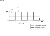
- FIG. 4 shows an example of luminance compensation at the time of black insertion drive.
- the horizontal axis represents time and the vertical axis represents brightness level.
- the waveform L11 shows the emission waveform of the OLED element during normal driving.
- the emission waveform of the normal drive always has a constant luminance level, indicates that the emission duty is 100% (Duty 100%) and the gain is 1 time (Gain ⁇ 1).
- Waveform L12 shows the light emission waveform of the OLED element when the black insertion is driven.
- the emission waveform of the black insertion drive is a rectangular wave, indicating that the emission duty is 50% (Duty 50%) and the gain is doubled (Gain ⁇ 2).
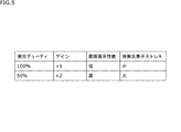
- FIG. 5 shows an example of the relationship between the light emission duty and gain, the moving image display performance, and the self-luminous element stress.
- a method of increasing the gain is used.
- the duty ratio is set to 100% and the gain is restored to minimize the temperature rise and stress of the LED etc., achieving both reliability and video performance. Further, in a fine image (a clear image frame having a high frequency component), a control for lowering the duty ratio is performed in order to enhance the effect of improving hold blur.
- the OLED display device has an OLED element as a self-luminous element, it is possible to control the light emission duty and improve the hold blur by changing the configuration of the drive circuit inside the display cell and performing black insertion drive. As mentioned earlier, it has become possible.
- the light emission duty is controlled according to parameters such as the amount of movement indicating the movement of the displayed object and the level of detail indicating the fineness of the image.
- the optimum duty value calculation unit 105 calculates the optimum light emission duty value using the amount of motion detected by the motion detection unit 103, thereby holding blurring the moving image. Make improvements in place.
- FIG. 6 shows an example of controlling the light emission duty according to the amount of movement.
- the horizontal axis represents the amount of motion (Motion)
- the vertical axis represents the light emission duty value.
- FIG. 6 it is shown that the movement amount of the displayed object in the image increases as the value on the horizontal axis moves to the right side, and the light emission duty value increases as the value on the vertical axis moves upward. Since hold blur is easily visible in an image including a display object having a large amount of movement, control is performed to reduce the light emission duty as shown by a polygonal line L21. On the other hand, in an image having a small amount of movement such as a still image, control is performed to increase the light emission duty as shown by the polygonal line L21. That is, the light emission duty value is lowered as the detected amount of movement increases.
- the optimum duty value calculation unit 105 calculates the optimum emission duty value using the detail level detected by the image flatness detection unit 101, so that the frequency component is high and clear. The hold blur is improved for the video (image frame including the edge).
- FIG. 7 shows an example of controlling the emission duty according to the level of detail.
- the horizontal axis represents the detail level (Detail_Lev), and the vertical axis represents the light emission duty value.
- FIG. 7 it is shown that the more the value on the horizontal axis goes to the right side, the finer the image includes more edge portions and the like, and the more the value on the vertical axis goes to the upper side, the higher the light emission duty value.
- control is performed to reduce the light emission duty as shown by the polygonal line L22.
- control is performed to increase the light emission duty as shown by the polygonal line L22. That is, the emission duty value decreases as the detected level of detail increases.
- the hold blur can be improved. Further, the stress of the OLED element can be reduced, and the decrease in the life of the OLED element can be suppressed.
- each pixel has a sub-pixel R that generates red (R) light, a sub-pixel G that generates green (G) light, a sub-pixel B that generates blue (B) light, and a white (W). It is composed of four sub-pixels of sub-pixel W that generate the light of.
- each pixel arranged two-dimensionally is an RGBW pixel.
- each pixel in the display area of the OLED display panel is RGBW pixel, but when lit at 100% level, the sub pixel R, the sub pixel G, and the sub pixel G are compared with the sub pixel W.
- the sub-pixel B has lower light emission efficiency and a larger current because it passes through a color filter corresponding to the wavelength band of each color. Therefore, the upper limit of the gain of the sub-pixel R, the sub-pixel G, and the sub-pixel B is lower than the gain of the sub-pixel W.
- complementary colors such as yellow (Y), magenta (M), and cyan (C) illuminate two sub-pixels in each pixel, so if they are lit at the maximum level as they are, the current limit value will be exceeded. It ends up.
- This current limit value depends on the temperature rise of the panel due to the self-heating of the OLED element and the limitation of the current capacity of the power supply.
- each pixel when the sub pixel R and the sub pixel G are lit, the color becomes yellow (Y), and when the sub pixel R and the sub pixel B are lit, the color becomes magenta (M), and the sub pixel G and the sub pixel B are displayed. When is lit, it becomes cyan (C).
- FIG. 8 shows an example of comparison of the drive current of the OLED element at the time of displaying each color.
- the horizontal axis represents the colors of the sub-pixels (W, R, G, B) and the colors (Y, M, C) when the sub-pixels are lit in two colors
- the vertical axis represents the EVDD current value. Shown.
- the EVDD current represents the total current flowing through the OLED element over the entire display area of the OLED display panel.
- the upper limit of the gain is lower.
- complementary colors such as yellow (Y), magenta (M), and cyan (C) exceed the current limit values shown by the broken lines in the figure when lit at the maximum level.
- the thick lines D1 to D3 the brightness level of the entire display area of the OLED display panel is lowered so as to be kept within the current limit value.
- the brightness of the sub-pixel W at the time of driving with black insertion for which brightness compensation is performed can be matched with the brightness at the time of driving without black insertion.
- the luminance level is the luminance of the input level 100%
- the luminance level of the sub-pixels R, G, and B is, for convenience, the luminance at the time of driving without black insertion as the luminance level of the sub-pixel W. It is said to be the same.
- the sub-pixel W can double the gain to compensate for the brightness, but the sub-pixels R, G, and B have an upper limit in gain, so the display area.
- the brightness level is lowered by lowering the light emission duty.
- FIG. 9 shows an example of peak brightness control at the time of black insertion drive for performing brightness compensation.
- the horizontal axis represents the average pixel level (APL) and the vertical axis represents the luminance level.
- the polygonal line L31 shows the control of the peak luminance of the sub-pixel W. Further, the polygonal lines L32 and L33 indicate the control of the peak luminance of the sub-pixels R, G, and B.
- the brightness level is lowered by setting the emission duty to 75% (Duty75%) in the region where the average pixel level is low. Can be avoided. In the region where the average pixel level is high, the emission duty is 50% (Duty50%) and 75% (Duty75%), which are almost the same brightness levels.
- the sub-pixels R, G, and B have a restriction that the upper limit value of the gain is lower than that of the sub-pixel W, the saturation of the highly saturated pixel is maintained even if the emission duty is lowered. Therefore, there is a problem that the gain cannot be raised sufficiently and the brightness is lowered. Therefore, in the present technology, in order to maintain the brightness balance between the low-saturation pixel and the high-saturation pixel, the lower limit value of the light emission duty is set according to the saturation level parameter.
- the optimum duty value calculation unit 105 calculates the optimum emission duty value using the saturation level detected by the saturation detection unit 102, so that the saturation is high. Make sure that the brightness balance between the low part and the low part is maintained.
- FIG. 10 shows an example of controlling the emission duty according to the saturation level.
- the horizontal axis represents the saturation level (Color_Sat_Lev), and the vertical axis represents the emission duty value.
- FIG. 10 it is shown that the more the value on the horizontal axis goes to the right, the higher the saturation becomes, and the more the value on the vertical axis goes to the upper side, the higher the emission duty value. If the emission duty is lowered for a large number of images, the brightness balance will be lost due to the upper limit of the gain of the sub-pixels R, G, and B. Therefore, as shown by the polygonal line L23, a lower limit value of the light emission duty is set according to the saturation level, and in an image having many high saturation regions, the light emission duty is controlled to be increased to obtain a pixel with high saturation. Ensure that the brightness balance of low pixels is maintained.
- Black crushing is a state in which the difference in brightness of a dark part cannot be sufficiently expressed and is filled like a solid black color.
- FIG. 11 shows an example of the gamma characteristic at the time of black insertion drive.
- the horizontal axis represents the input level and the vertical axis represents the output level.
- the straight line L41 indicates the target gamma value (2.2).
- the polygonal line L42 indicates a normal drive in which the light emission duty is 100% (Duty 100%) and the gain is 1 times (Gain ⁇ 1).
- the polygonal line L43 indicates a black insertion drive in which the light emission duty is 50% (Duty 50%) and the gain is doubled (Gain ⁇ 2).
- FIG. 12 shows an example of the effective light emission period during the normal drive and the black insertion drive.
- the horizontal axis represents time and the vertical axis represents voltage level.
- FIG. 12A shows the voltage fluctuation of the OLED element during normal driving, and the time after the voltage level indicated by the waveform L51 exceeds the threshold voltage Vth for each frame is the effective light emission period T1.
- FIG. 12B shows the voltage fluctuation of the OLED element during the black insertion drive, and the time after the voltage level indicated by the waveform L52 for each frame exceeds the threshold voltage Vth is the effective light emission period T2.
- the effective light emitting period T2 during the black insertion drive is shorter than the effective light emitting period T1 during the normal drive.
- the OLED element when the OLED element is driven with black insertion, the lower the gradation level, the greater the effect on the drive duty due to the rising characteristics of light emission. Therefore, when performing black insertion drive as a measure against hold blur, the light emission duty is set. As the value is lowered, the effective light emission period in the low gradation region is reduced, the brightness is significantly reduced, and black crushing tends to occur.
- the optimum duty value calculation unit 105 calculates the optimum emission duty value using the average pixel level (APL) detected by the APL detection unit 104, thereby lowering the order. Suppression of brightness reduction at the tuning level is implemented.
- APL average pixel level
- FIG. 13 shows an example of controlling the emission duty according to the average pixel level (APL).
- the horizontal axis represents the average pixel level (Ave_Pix_Lev), and the vertical axis represents the light emission duty value.
- Offset control In the above description, control of the emission duty according to the average pixel level (APL) has been described as a countermeasure for the decrease in brightness at a low gradation level when the OLED element is driven by inserting black, but other methods are used. It doesn't matter.
- the offset control unit 108 calculates an offset value related to the brightness of the video signal based on the light emission duty value calculated by the optimum duty value calculation unit 105, and adds the offset value to the video signal. May be performed so that the brightness is corrected.
- the offset value of the video signal By controlling the offset value of the video signal according to the light emission duty value in this way, the decrease in brightness at the low gradation level can be suppressed, and as a result, blackout can be suppressed.
- the gamma characteristic is corrected by correcting the brightness by the offset value.
- the OLED display panel is configured by arranging a plurality of OLED elements in a two-dimensional manner, a scan for a black signal is required to turn off each OLED element.
- the black insertion drive is performed, the light emitting region changes within one frame, and the current fluctuates.
- FIG. 14 shows an example of current fluctuation of the power supply circuit for driving the OLED element.
- the horizontal axis represents time and the vertical axis represents E VDD current value.
- the polygonal line L61 shows the temporal fluctuation of the EVDD current value. Further, in FIG. 14, the images I1 to I6 in one frame are arranged in time series, and correspond to the temporal fluctuation of the EVDD current value indicated by the polygonal line L61.
- the straight line L62 indicates a peak current limit value, and is controlled so that the peak current does not exceed this limit value. Further, the straight line L63 indicates an average current limit value, and is controlled so that the average current does not exceed this limit value.
- Image I is an image consisting of a monochromatic window represented by a dot pattern and a black background.
- the black insertion drive is performed, the light emitting region corresponding to the monochromatic window in the image I changes within one image frame as in the images I1 to I6.
- the EVDD current value indicated by the polygonal line L61 fluctuates according to this light emitting region.
- the frame FR on the image I indicates an area in which a black signal for black insertion is displayed in the frame.
- images I1 to I6 since the black insertion is performed from the upper side to the lower side, the scan proceeds downward and the displayed signal is updated from the upper side. That is, the black insertion area in the frame FR moves downward.
- the peak current increases by the average current ⁇ the gain, so that the EVDD current value indicated by the broken line L61 exceeds the peak current limit value.
- the E VDD current value is set to approximately 0.
- the average current of one frame can be set to the same value as when the black insertion drive is not performed, but since the light emitting region changes within one frame, the current There is a problem that there is fluctuation and it must be suppressed within the peak current value that the drive power supply circuit can tolerate. Therefore, in the present technology, the calculation method of the current limit is corrected according to the gain for luminance compensation, and the control is performed so that the peak current becomes a certain value or less.
- the calculated value of the peak current is corrected according to the gain, and even in the case where the peak current in which the load is concentrated is the maximum, the peak current limit value is not exceeded, for example, the peak current limit value is exceeded. It is possible to control the average current value to decrease according to the gain ratio.
- the peak current control unit 107 controls the peak current based on the gain calculated by the gain calculation unit 106 to limit the peak current to the peak current of the drive power supply circuit. Try to keep it within the value.
- FIG. 15 shows an example of peak current control.
- the horizontal axis represents time and the vertical axis represents E VDD current value.
- the polygonal line L71 shows the temporal fluctuation of the E VDD current value when the peak current control is not performed.
- the polygonal line L72 shows the temporal variation of the EVDD current value when the peak current is controlled.
- the straight line L73 indicates the peak current limit value. Further, the straight line L74 indicates an average current limit value.
- the limits regarding the current value in the drive power supply circuit include the limit of the average current value and the limit of the peak current value. If the peak current is not limited, the peak current value increases by a maximum of 1 / Duty. In the end (for example, in the case of Duty 50%, it is up to twice), and the peak current limit value is exceeded.
- the gain increased by the luminance compensation at the time of black insertion drive is controlled so as to be a value represented by the following equation (1).
- the peak current exceeds the peak current limit value L73 as shown by the polygonal line L71, but by performing the peak current control, it is shown by the polygonal line L72. , The peak current is controlled within the peak current limit value L73. As a result, the reliability of the drive power supply circuit can be ensured.
- FIG. 16 shows an example of the configuration of an embodiment of a self-luminous display device to which the present technology is applied.
- the self-luminous display device 1 is configured as a television receiver or the like.
- the self-luminous display device 1 includes a signal input unit 111, a signal processing unit 112, a display panel drive unit 113, and a self-luminous display panel 114.
- the signal processing unit 112 corresponds to the signal processing device 10 of FIG. 1
- the display panel driving unit 113 corresponds to the panel driver 20 of FIG.
- the signal input unit 111 is composed of a tuner connected to an antenna, a communication module that can be connected to a communication network such as the Internet, an input interface conforming to a predetermined standard, and the like.
- the signal input unit 111 records broadcast content transmitted by terrestrial broadcasting, satellite broadcasting, etc., communication content streamed via a communication network such as the Internet, or a recording medium such as an optical disk or semiconductor memory, a recorder, or the like. Video signals of various contents such as recorded contents are supplied to the signal processing unit 112.
- the signal processing unit 112 performs predetermined video signal processing based on the video signal of the content supplied from the signal input unit 111.
- a video signal and a control signal for controlling the drive of the self-luminous display panel 114 are generated and supplied to the display panel drive unit 113.
- the control signal includes parameters such as emission duty value (Duty), gain (Gain), current limit value (Cur_ratio), or offset value (offset).
- the display panel drive unit 113 drives the self-luminous display panel 114 based on the video signal and the control signal supplied from the signal processing unit 112.
- the self-luminous display panel 114 is a display panel in which pixels including self-luminous elements are arranged in a two-dimensional manner, and displays an image according to the drive from the display panel driving unit 113.
- the self-luminous display panel 114 an OLED display panel using an OLED element as the self-luminous element can be adopted.
- the self-luminous display device 1 is an OLED display device.
- the minimum configuration is shown for the sake of simplification of the description, but there are other devices such as an audio signal processing circuit that processes an audio signal and a speaker that outputs an audio according to the audio signal. Circuits and devices may be included.
- the optimum duty value calculation unit 105 calculates the light emission duty value
- one of the four parameters (Detail_Lev, Color_Sat_Lev, Motion, Ave_Pix_Lev) is of course used, and a plurality of parameters are used.
- the emission duty value may be calculated using the parameters of.
- the plurality of controls described above, for example, current control by the peak current control unit 107 and offset value control by the offset calculation unit 108 may be performed at the same time.
- the self-luminous display device 1 is a television receiver
- examples of the electronic device using the self-luminous display device 1 include a display device, a personal computer, and a tablet computer. It may be a smartphone, a mobile phone, a digital camera, a head mount display, a game machine, or the like.
- the self-luminous display device 1 may be used as a display unit for in-vehicle devices such as car navigation systems and rear seat monitors, or wearable devices such as wristwatch type and eyeglass type.
- the display device includes, for example, a medical monitor, a broadcasting monitor, a display for digital signage, and the like.
- OLED may be read as “organic EL”.
- the OLED display device can be said to be an organic EL display device.
- hold blur is also referred to as motion blur
- hold blur may be read as “movement blur”.
- video since the video is composed of a plurality of image frames, "video” may be read as "image”.
- a detector that analyzes the video signal of the content and detects an index that correlates with hold blur, A first calculation unit that calculates the light emission duty value of the self-luminous display panel based on the detected index, and A signal processing device including a second calculation unit that calculates a gain for luminance compensation based on the calculated emission duty value.
- the detection unit detects the amount of movement of the object displayed on the self-luminous display panel, and detects the amount of movement of the object.
- the signal processing device according to (1), wherein the first calculation unit calculates the light emission duty value according to the detected movement amount.
- the first calculation unit lowers the light emission duty value as the detected movement amount increases.
- the detection unit detects the level of detail of the image displayed on the self-luminous display panel.
- the signal processing device according to any one of (1) to (3), wherein the first calculation unit calculates the light emission duty value according to the detected detailed level.
- the first calculation unit lowers the emission duty value as the detected level of detail increases.
- the signal processing device according to (4), wherein the second calculation unit raises the gain in response to a change in the light emission duty value.
- the detection unit detects the saturation level of the image displayed on the self-luminous display panel.
- the signal processing device according to any one of (1) to (5), wherein the first calculation unit calculates the emission duty value according to the detected saturation level.
- the signal processing device according to (6), wherein the first calculation unit sets a limit on the lower limit of the emission duty value according to the detected saturation level.
- the detection unit detects the average pixel level of the video signal and The signal processing device according to any one of (1) to (7), wherein the first calculation unit calculates the light emission duty value according to the detected average pixel level.
- the first calculation unit sets a limit on the lower limit of the emission duty value, and increases the emission duty value as the average pixel level decreases.
- the signal processing device according to (8).
- the control unit (1) to (9) further includes a control unit that controls the current flowing through the self-luminous element arranged in the self-luminous display panel according to the gain so as to be suppressed within an allowable peak current by the power supply circuit. ).
- the signal processing device according to any one of. (11)
- the control unit controls so that the light emitting region of the self-luminous display panel does not exceed the peak current limit value when the peak current becomes maximum when the current fluctuation occurs due to a change within one frame of the image.
- (12) The signal processing device according to (11) above, wherein the control unit controls the gain to be a value obtained by dividing a peak current limit value by an average current limit value.
- the signal processing device according to any one of (1) to (12), further comprising a third calculation unit for calculating an offset value relating to the brightness of the video signal according to the light emission duty value.
- the signal processing apparatus according to (13), wherein the offset value corrects a decrease in brightness at a low gradation level.
- the signal processing device according to any one of (1) to (14) above, wherein the light emission duty is reduced by a black insertion drive provided with a black display period during the display period for displaying the same image.
- the gain is obtained by the reciprocal of the light emission duty value.
- the self-luminous display panel has a first sub-pixel that generates red (R) light, a second sub-pixel that generates green (G) light, and a third sub that generates blue (B) light.
- the signal processing apparatus according to any one of (1) to (16) above, wherein the pixels and the pixels having the fourth sub-pixels that generate white (W) light are arranged in a two-dimensional manner.
- the pixel includes an OLED (Organic Light Emitting Diode) element as a self-luminous element.
- the signal processing device Analyze the video signal of the content to detect the index that correlates with the hold blur, Based on the detected index, the light emission duty value of the self-luminous display panel is calculated.
- a signal processing method for calculating a gain for luminance compensation based on the calculated emission duty value (20) A signal processing unit that processes the video signal of the content, A self-luminous display panel that displays the video of the content, and A display panel drive unit that drives the self-luminous display panel based on a video signal from the signal processing unit is provided.
- the signal processing unit A detection unit that analyzes the video signal of the content and detects an index that correlates with hold blur.
- a first calculation unit that calculates the light emission duty value of the self-luminous display panel based on the detected index, and It has a second calculation unit that calculates the gain for luminance compensation based on the calculated emission duty value.
- the display panel drive unit is a display device that drives the self-luminous display panel based on the light emission duty value and the gain calculated by the signal processing unit.
- 1 Self-luminous display device 10 signal processing device, 20 panel driver, 30 signal line, 40 control line, 100 detection unit, 101 image flatness detection unit, 102 saturation detection unit, 103 motion detection unit, 104 APL detection unit , 105 Optimal duty value calculation unit, 106 Gain calculation unit, 107 Peak current control unit, 108 Offset calculation unit, 111 Signal input unit, 112 Signal processing unit, 113 Display panel drive unit, 114 Self-luminous display panel
Abstract
La présente technologie concerne un dispositif de traitement de signal, un procédé de traitement de signal et un dispositif d'affichage qui permettent d'améliorer le flou de maintien de façon plus appropriée. L'invention concerne un dispositif de traitement de signal comprenant : une unité de détection qui analyse le signal vidéo d'un contenu et qui détecte un indice qui est en corrélation avec le flou de maintien; une première unité de calcul qui calcule une valeur de rapport cyclique d'émission de lumière d'un panneau d'affichage auto-lumineux sur la base de l'indice détecté; et une seconde unité de calcul qui calcule un gain pour la compensation de luminance sur la base de la valeur de rapport cyclique d'émission de lumière calculée. La présente technologie peut être appliquée, par exemple, à un dispositif d'imagerie auto-lumineux.
Priority Applications (4)
| Application Number | Priority Date | Filing Date | Title |
|---|---|---|---|
| JP2021567265A JPWO2021131830A1 (fr) | 2019-12-27 | 2020-12-14 | |
| EP20905180.4A EP4083983A4 (fr) | 2019-12-27 | 2020-12-14 | Dispositif de traitement de signal, procédé de traitement de signal et dispositif d'affichage |
| CN202080088009.6A CN114846534A (zh) | 2019-12-27 | 2020-12-14 | 信号处理装置、信号处理方法以及显示装置 |
| US17/757,768 US20230018404A1 (en) | 2019-12-27 | 2020-12-14 | Signal processing device, signal processing method, and display device |
Applications Claiming Priority (2)
| Application Number | Priority Date | Filing Date | Title |
|---|---|---|---|
| JP2019-238105 | 2019-12-27 | ||
| JP2019238105 | 2019-12-27 |
Publications (1)
| Publication Number | Publication Date |
|---|---|
| WO2021131830A1 true WO2021131830A1 (fr) | 2021-07-01 |
Family
ID=76574424
Family Applications (1)
| Application Number | Title | Priority Date | Filing Date |
|---|---|---|---|
| PCT/JP2020/046460 WO2021131830A1 (fr) | 2019-12-27 | 2020-12-14 | Dispositif de traitement de signal, procédé de traitement de signal et dispositif d'affichage |
Country Status (5)
| Country | Link |
|---|---|
| US (1) | US20230018404A1 (fr) |
| EP (1) | EP4083983A4 (fr) |
| JP (1) | JPWO2021131830A1 (fr) |
| CN (1) | CN114846534A (fr) |
| WO (1) | WO2021131830A1 (fr) |
Families Citing this family (2)
| Publication number | Priority date | Publication date | Assignee | Title |
|---|---|---|---|---|
| KR20210129310A (ko) * | 2020-04-17 | 2021-10-28 | 삼성디스플레이 주식회사 | 표시 장치 및 그 구동 방법 |
| KR20220084602A (ko) * | 2020-12-14 | 2022-06-21 | 엘지디스플레이 주식회사 | 전계 발광 표시장치와 그 구동방법 |
Citations (8)
| Publication number | Priority date | Publication date | Assignee | Title |
|---|---|---|---|---|
| JP2004252216A (ja) * | 2003-02-20 | 2004-09-09 | Hitachi Ltd | 自発光型表示装置とその駆動方法 |
| JP2006189658A (ja) * | 2005-01-06 | 2006-07-20 | Toshiba Corp | 画像表示装置及びその画像表示方法 |
| JP2008139797A (ja) * | 2006-12-05 | 2008-06-19 | Semiconductor Energy Lab Co Ltd | 表示装置およびその駆動方法 |
| WO2008153055A1 (fr) * | 2007-06-13 | 2008-12-18 | Sony Corporation | Dispositif d'affichage, procédé et programme de traitement de signaux vidéo |
| JP2010160237A (ja) * | 2009-01-07 | 2010-07-22 | Seiko Epson Corp | 発光制御信号生成方法、発光制御信号生成回路、表示装置、電子機器 |
| US20160155382A1 (en) * | 2014-11-27 | 2016-06-02 | Samsung Display Co., Ltd. | Display device and method of driving the display device |
| JP2018151666A (ja) * | 2018-06-08 | 2018-09-27 | 双葉電子工業株式会社 | 表示駆動装置、表示装置、表示駆動方法 |
| WO2019124254A1 (fr) | 2017-12-19 | 2019-06-27 | ソニー株式会社 | Dispositif de traitement de signal, procédé de traitement de signal et dispositif d'affichage |
Family Cites Families (6)
| Publication number | Priority date | Publication date | Assignee | Title |
|---|---|---|---|---|
| JP4433041B2 (ja) * | 2007-11-16 | 2010-03-17 | ソニー株式会社 | 表示装置、画像信号処理方法、およびプログラム |
| JP2010015008A (ja) * | 2008-07-04 | 2010-01-21 | Samsung Electronics Co Ltd | 映像信号処理装置、映像信号処理方法、プログラム、および表示装置 |
| TW201445542A (zh) * | 2013-05-20 | 2014-12-01 | Sony Corp | 影像信號處理電路、影像信號處理方法及顯示裝置 |
| CN105489170B (zh) * | 2014-09-16 | 2019-08-06 | 青岛海信电器股份有限公司 | 一种背光源的驱动方法、装置及显示设备 |
| US10497321B2 (en) * | 2017-10-31 | 2019-12-03 | Wuhan China Star Optoelectronics Technology Co., Ltd. | Image processing method and device thereof |
| CN109360530B (zh) * | 2018-10-30 | 2023-06-27 | 武汉华星光电技术有限公司 | 液晶显示装置及其背光控制方法 |
-
2020
- 2020-12-14 JP JP2021567265A patent/JPWO2021131830A1/ja active Pending
- 2020-12-14 CN CN202080088009.6A patent/CN114846534A/zh active Pending
- 2020-12-14 WO PCT/JP2020/046460 patent/WO2021131830A1/fr unknown
- 2020-12-14 US US17/757,768 patent/US20230018404A1/en active Pending
- 2020-12-14 EP EP20905180.4A patent/EP4083983A4/fr active Pending
Patent Citations (8)
| Publication number | Priority date | Publication date | Assignee | Title |
|---|---|---|---|---|
| JP2004252216A (ja) * | 2003-02-20 | 2004-09-09 | Hitachi Ltd | 自発光型表示装置とその駆動方法 |
| JP2006189658A (ja) * | 2005-01-06 | 2006-07-20 | Toshiba Corp | 画像表示装置及びその画像表示方法 |
| JP2008139797A (ja) * | 2006-12-05 | 2008-06-19 | Semiconductor Energy Lab Co Ltd | 表示装置およびその駆動方法 |
| WO2008153055A1 (fr) * | 2007-06-13 | 2008-12-18 | Sony Corporation | Dispositif d'affichage, procédé et programme de traitement de signaux vidéo |
| JP2010160237A (ja) * | 2009-01-07 | 2010-07-22 | Seiko Epson Corp | 発光制御信号生成方法、発光制御信号生成回路、表示装置、電子機器 |
| US20160155382A1 (en) * | 2014-11-27 | 2016-06-02 | Samsung Display Co., Ltd. | Display device and method of driving the display device |
| WO2019124254A1 (fr) | 2017-12-19 | 2019-06-27 | ソニー株式会社 | Dispositif de traitement de signal, procédé de traitement de signal et dispositif d'affichage |
| JP2018151666A (ja) * | 2018-06-08 | 2018-09-27 | 双葉電子工業株式会社 | 表示駆動装置、表示装置、表示駆動方法 |
Non-Patent Citations (1)
| Title |
|---|
| See also references of EP4083983A4 |
Also Published As
| Publication number | Publication date |
|---|---|
| CN114846534A (zh) | 2022-08-02 |
| US20230018404A1 (en) | 2023-01-19 |
| JPWO2021131830A1 (fr) | 2021-07-01 |
| EP4083983A1 (fr) | 2022-11-02 |
| EP4083983A4 (fr) | 2023-05-03 |
Similar Documents
| Publication | Publication Date | Title |
|---|---|---|
| EP3098803B1 (fr) | Procédé de traitement d'image, circuit de traitement d'image et dispositif d'affichage à diode électroluminescente organique utilisant celui-ci | |
| RU2497168C2 (ru) | Жидкокристаллический дисплей | |
| US8593391B2 (en) | Liquid crystal display device control circuit and liquid crystal display system, which adjust brightness of display image by using height distribution of gradations of input image | |
| US9183797B2 (en) | Display device and control method for display device | |
| EP3223266B1 (fr) | Dispositif d'affichage à diodes électroluminescentes organiques et son procédé de fonctionnement | |
| KR20100007748A (ko) | 표시 장치, 표시 장치의 구동 방법, 구동용 집적 회로, 구동용 집적 회로에 의한 구동 방법 및 신호 처리 방법 | |
| US9990878B2 (en) | Data clipping method using red, green, blue and white data, and display device using the same | |
| KR102385628B1 (ko) | 표시장치 및 그의 구동방법 | |
| US11942049B2 (en) | Signal processing apparatus, signal processing method, and display apparatus | |
| WO2021131830A1 (fr) | Dispositif de traitement de signal, procédé de traitement de signal et dispositif d'affichage | |
| KR102510573B1 (ko) | 투명 표시 장치 및 그 구동 방법 | |
| KR20160035192A (ko) | 표시장치와 그 휘도 향상 방법 | |
| US20230410733A1 (en) | Signal Processing Apparatus, Signal Processing Method, And Display Apparatus | |
| JP2008176111A (ja) | 画像表示装置および画像表示方法 | |
| US20230162668A1 (en) | Signal Processing Device, Signal Processing Method, And Display Device | |
| KR101611907B1 (ko) | 표시 장치의 색 보정 방법 및 장치 | |
| KR101870991B1 (ko) | 표시 장치의 색 보정장치 및 방법 | |
| JP2013250562A (ja) | 表示装置、映像種別判定装置、表示装置の駆動方法、及び映像種別の判定方法 | |
| KR102666134B1 (ko) | 표시 장치 | |
| KR20140092159A (ko) | 표시 장치 및 그 구동 방법 |
Legal Events
| Date | Code | Title | Description |
|---|---|---|---|
| 121 | Ep: the epo has been informed by wipo that ep was designated in this application |
Ref document number: 20905180 Country of ref document: EP Kind code of ref document: A1 |
|
| ENP | Entry into the national phase |
Ref document number: 2021567265 Country of ref document: JP Kind code of ref document: A |
|
| NENP | Non-entry into the national phase |
Ref country code: DE |
|
| ENP | Entry into the national phase |
Ref document number: 2020905180 Country of ref document: EP Effective date: 20220727 |