WO2021206069A1 - 半導体封止成形用仮保護フィルム及びその製造方法、仮保護フィルム付きリードフレーム、仮保護された封止成形体、並びに、半導体パッケージを製造する方法 - Google Patents
半導体封止成形用仮保護フィルム及びその製造方法、仮保護フィルム付きリードフレーム、仮保護された封止成形体、並びに、半導体パッケージを製造する方法 Download PDFInfo
- Publication number
- WO2021206069A1 WO2021206069A1 PCT/JP2021/014555 JP2021014555W WO2021206069A1 WO 2021206069 A1 WO2021206069 A1 WO 2021206069A1 JP 2021014555 W JP2021014555 W JP 2021014555W WO 2021206069 A1 WO2021206069 A1 WO 2021206069A1
- Authority
- WO
- WIPO (PCT)
- Prior art keywords
- protective film
- lead frame
- temporary protective
- adhesive layer
- sealing
- Prior art date
- Legal status (The legal status is an assumption and is not a legal conclusion. Google has not performed a legal analysis and makes no representation as to the accuracy of the status listed.)
- Ceased
Links
Images




Classifications
-
- C—CHEMISTRY; METALLURGY
- C09—DYES; PAINTS; POLISHES; NATURAL RESINS; ADHESIVES; COMPOSITIONS NOT OTHERWISE PROVIDED FOR; APPLICATIONS OF MATERIALS NOT OTHERWISE PROVIDED FOR
- C09J—ADHESIVES; NON-MECHANICAL ASPECTS OF ADHESIVE PROCESSES IN GENERAL; ADHESIVE PROCESSES NOT PROVIDED FOR ELSEWHERE; USE OF MATERIALS AS ADHESIVES
- C09J7/00—Adhesives in the form of films or foils
- C09J7/30—Adhesives in the form of films or foils characterised by the adhesive composition
-
- C—CHEMISTRY; METALLURGY
- C08—ORGANIC MACROMOLECULAR COMPOUNDS; THEIR PREPARATION OR CHEMICAL WORKING-UP; COMPOSITIONS BASED THEREON
- C08K—Use of inorganic or non-macromolecular organic substances as compounding ingredients
- C08K5/00—Use of organic ingredients
- C08K5/04—Oxygen-containing compounds
- C08K5/15—Heterocyclic compounds having oxygen in the ring
- C08K5/151—Heterocyclic compounds having oxygen in the ring having one oxygen atom in the ring
- C08K5/1515—Three-membered rings
-
- C—CHEMISTRY; METALLURGY
- C09—DYES; PAINTS; POLISHES; NATURAL RESINS; ADHESIVES; COMPOSITIONS NOT OTHERWISE PROVIDED FOR; APPLICATIONS OF MATERIALS NOT OTHERWISE PROVIDED FOR
- C09J—ADHESIVES; NON-MECHANICAL ASPECTS OF ADHESIVE PROCESSES IN GENERAL; ADHESIVE PROCESSES NOT PROVIDED FOR ELSEWHERE; USE OF MATERIALS AS ADHESIVES
- C09J11/00—Features of adhesives not provided for in group C09J9/00, e.g. additives
- C09J11/02—Non-macromolecular additives
- C09J11/06—Non-macromolecular additives organic
-
- C—CHEMISTRY; METALLURGY
- C09—DYES; PAINTS; POLISHES; NATURAL RESINS; ADHESIVES; COMPOSITIONS NOT OTHERWISE PROVIDED FOR; APPLICATIONS OF MATERIALS NOT OTHERWISE PROVIDED FOR
- C09J—ADHESIVES; NON-MECHANICAL ASPECTS OF ADHESIVE PROCESSES IN GENERAL; ADHESIVE PROCESSES NOT PROVIDED FOR ELSEWHERE; USE OF MATERIALS AS ADHESIVES
- C09J201/00—Adhesives based on unspecified macromolecular compounds
-
- H—ELECTRICITY
- H10—SEMICONDUCTOR DEVICES; ELECTRIC SOLID-STATE DEVICES NOT OTHERWISE PROVIDED FOR
- H10W—GENERIC PACKAGES, INTERCONNECTIONS, CONNECTORS OR OTHER CONSTRUCTIONAL DETAILS OF DEVICES COVERED BY CLASS H10
- H10W72/00—Interconnections or connectors in packages
-
- H—ELECTRICITY
- H10—SEMICONDUCTOR DEVICES; ELECTRIC SOLID-STATE DEVICES NOT OTHERWISE PROVIDED FOR
- H10W—GENERIC PACKAGES, INTERCONNECTIONS, CONNECTORS OR OTHER CONSTRUCTIONAL DETAILS OF DEVICES COVERED BY CLASS H10
- H10W74/00—Encapsulations, e.g. protective coatings
- H10W74/01—Manufacture or treatment
-
- H—ELECTRICITY
- H10—SEMICONDUCTOR DEVICES; ELECTRIC SOLID-STATE DEVICES NOT OTHERWISE PROVIDED FOR
- H10W—GENERIC PACKAGES, INTERCONNECTIONS, CONNECTORS OR OTHER CONSTRUCTIONAL DETAILS OF DEVICES COVERED BY CLASS H10
- H10W74/00—Encapsulations, e.g. protective coatings
- H10W74/01—Manufacture or treatment
- H10W74/014—Manufacture or treatment using batch processing
-
- H—ELECTRICITY
- H10—SEMICONDUCTOR DEVICES; ELECTRIC SOLID-STATE DEVICES NOT OTHERWISE PROVIDED FOR
- H10W—GENERIC PACKAGES, INTERCONNECTIONS, CONNECTORS OR OTHER CONSTRUCTIONAL DETAILS OF DEVICES COVERED BY CLASS H10
- H10W74/00—Encapsulations, e.g. protective coatings
- H10W74/01—Manufacture or treatment
- H10W74/019—Manufacture or treatment using temporary auxiliary substrates
-
- C—CHEMISTRY; METALLURGY
- C09—DYES; PAINTS; POLISHES; NATURAL RESINS; ADHESIVES; COMPOSITIONS NOT OTHERWISE PROVIDED FOR; APPLICATIONS OF MATERIALS NOT OTHERWISE PROVIDED FOR
- C09J—ADHESIVES; NON-MECHANICAL ASPECTS OF ADHESIVE PROCESSES IN GENERAL; ADHESIVE PROCESSES NOT PROVIDED FOR ELSEWHERE; USE OF MATERIALS AS ADHESIVES
- C09J2203/00—Applications of adhesives in processes or use of adhesives in the form of films or foils
- C09J2203/326—Applications of adhesives in processes or use of adhesives in the form of films or foils for bonding electronic components such as wafers, chips or semiconductors
-
- C—CHEMISTRY; METALLURGY
- C09—DYES; PAINTS; POLISHES; NATURAL RESINS; ADHESIVES; COMPOSITIONS NOT OTHERWISE PROVIDED FOR; APPLICATIONS OF MATERIALS NOT OTHERWISE PROVIDED FOR
- C09J—ADHESIVES; NON-MECHANICAL ASPECTS OF ADHESIVE PROCESSES IN GENERAL; ADHESIVE PROCESSES NOT PROVIDED FOR ELSEWHERE; USE OF MATERIALS AS ADHESIVES
- C09J2301/00—Additional features of adhesives in the form of films or foils
- C09J2301/30—Additional features of adhesives in the form of films or foils characterized by the chemical, physicochemical or physical properties of the adhesive or the carrier
- C09J2301/312—Additional features of adhesives in the form of films or foils characterized by the chemical, physicochemical or physical properties of the adhesive or the carrier parameters being the characterizing feature
-
- H—ELECTRICITY
- H10—SEMICONDUCTOR DEVICES; ELECTRIC SOLID-STATE DEVICES NOT OTHERWISE PROVIDED FOR
- H10W—GENERIC PACKAGES, INTERCONNECTIONS, CONNECTORS OR OTHER CONSTRUCTIONAL DETAILS OF DEVICES COVERED BY CLASS H10
- H10W72/00—Interconnections or connectors in packages
- H10W72/01—Manufacture or treatment
- H10W72/0198—Manufacture or treatment batch processes
-
- H—ELECTRICITY
- H10—SEMICONDUCTOR DEVICES; ELECTRIC SOLID-STATE DEVICES NOT OTHERWISE PROVIDED FOR
- H10W—GENERIC PACKAGES, INTERCONNECTIONS, CONNECTORS OR OTHER CONSTRUCTIONAL DETAILS OF DEVICES COVERED BY CLASS H10
- H10W72/00—Interconnections or connectors in packages
- H10W72/071—Connecting or disconnecting
- H10W72/075—Connecting or disconnecting of bond wires
-
- H—ELECTRICITY
- H10—SEMICONDUCTOR DEVICES; ELECTRIC SOLID-STATE DEVICES NOT OTHERWISE PROVIDED FOR
- H10W—GENERIC PACKAGES, INTERCONNECTIONS, CONNECTORS OR OTHER CONSTRUCTIONAL DETAILS OF DEVICES COVERED BY CLASS H10
- H10W72/00—Interconnections or connectors in packages
- H10W72/50—Bond wires
-
- H—ELECTRICITY
- H10—SEMICONDUCTOR DEVICES; ELECTRIC SOLID-STATE DEVICES NOT OTHERWISE PROVIDED FOR
- H10W—GENERIC PACKAGES, INTERCONNECTIONS, CONNECTORS OR OTHER CONSTRUCTIONAL DETAILS OF DEVICES COVERED BY CLASS H10
- H10W74/00—Encapsulations, e.g. protective coatings
-
- H—ELECTRICITY
- H10—SEMICONDUCTOR DEVICES; ELECTRIC SOLID-STATE DEVICES NOT OTHERWISE PROVIDED FOR
- H10W—GENERIC PACKAGES, INTERCONNECTIONS, CONNECTORS OR OTHER CONSTRUCTIONAL DETAILS OF DEVICES COVERED BY CLASS H10
- H10W74/00—Encapsulations, e.g. protective coatings
- H10W74/10—Encapsulations, e.g. protective coatings characterised by their shape or disposition
- H10W74/111—Encapsulations, e.g. protective coatings characterised by their shape or disposition the semiconductor body being completely enclosed
-
- H—ELECTRICITY
- H10—SEMICONDUCTOR DEVICES; ELECTRIC SOLID-STATE DEVICES NOT OTHERWISE PROVIDED FOR
- H10W—GENERIC PACKAGES, INTERCONNECTIONS, CONNECTORS OR OTHER CONSTRUCTIONAL DETAILS OF DEVICES COVERED BY CLASS H10
- H10W90/00—Package configurations
- H10W90/701—Package configurations characterised by the relative positions of pads or connectors relative to package parts
- H10W90/751—Package configurations characterised by the relative positions of pads or connectors relative to package parts of bond wires
- H10W90/756—Package configurations characterised by the relative positions of pads or connectors relative to package parts of bond wires between a chip and a stacked lead frame, conducting package substrate or heat sink
Definitions
- the present invention relates to a temporary protective film for semiconductor encapsulation molding and a method for manufacturing the same, a lead frame with a temporary protective film, a temporarily protected encapsulation molded product, and a method for manufacturing a semiconductor package.
- Patent Documents 1 and 2 a structure in which a sealing layer is formed only on the semiconductor element side of the lead frame and the back surface of the lead frame is exposed may be adopted (Patent Documents 1 and 2).
- the back surface of the lead frame may be temporarily protected by attaching a temporary protective film. The temporary protective film is peeled off from the lead frame after the sealing layer is formed.
- the assembly process for manufacturing a semiconductor package may require heating at a high temperature of up to about 400 ° C for reflow connection or the like.
- a high temperature of up to about 400 ° C for reflow connection or the like.
- the temporary protective film attached to the lead frame receives a heat history at such a high temperature, the temporary protective film and the lead frame and the sealing layer are firmly adhered to each other, and the temporary protective film is peeled off from the lead frame. In some cases, it was not possible to remove the lead frame cleanly without leaving a residue.
- the present disclosure is a temporary protective film for semiconductor encapsulation molding that can be attached to a lead frame with an appropriate adhesive force and can be easily peeled off after receiving a heat history of a high temperature of about 400 ° C. Regarding.
- One aspect of the present disclosure provides a temporary protective film including a support film and an adhesive layer provided on one or both sides of the support film.
- This temporary protective film is used to temporarily protect the surface of the lead frame opposite to the semiconductor element during sealing molding to form a sealing layer for sealing the semiconductor element mounted on the die pad of the lead frame. Used for.
- one aspect of the present disclosure is that during the sealing molding of the temporary protective film to form a sealing layer that seals the semiconductor element mounted on the die pad of the lead frame, the semiconductor element of the lead frame An application is provided to provide temporary protection for the opposite surface.
- the adhesive layer is a sticker made of the copper plate and the temporary protective film for semiconductor encapsulation by attaching the temporary protective film for semiconductor encapsulation molding to the surface of the copper plate in a direction in which the adhesive layer is in contact with the copper plate.
- the ratio of oxygen atoms on the surface of the copper plate after heating the patch at 180 ° C. for 1 hour is X1, and then the patch is further heated at 400 ° C. for 2 minutes for heat treatment.
- X2 is smaller than X1.
- the protective film for semiconductor encapsulation molding is attached to the surface of the copper plate in a direction in which the adhesive layer is in contact with the copper plate, and then a sticker made of the copper plate and the temporary protective film for semiconductor encapsulation molding is attached to 180.
- the proportion of oxygen atoms on the surface of the copper plate after heating at 180 ° C. for 1 hour is 2 minutes at 400 ° C.
- the proportion of oxygen atoms on the surface of the copper plate after heating is small.
- Another aspect of the present disclosure provides a method of manufacturing a temporary protective film comprising a support film and an adhesive layer provided on one or both sides of the support film.
- the manufactured temporary protective film temporarily protects the surface of the lead frame opposite to the semiconductor element during sealing molding to form a sealing layer for sealing the semiconductor element mounted on the die pad of the lead frame.
- It is a protective film for semiconductor encapsulation molding used for this purpose.
- an adhesive layer consisting of 100 parts by mass of a thermoplastic resin and 5 to 20 parts by mass of a low molecular weight additive is attached to the surface of a copper plate to form a sticker made of the copper plate and the adhesive layer, and the sticker is formed.
- the method comprises attaching an adhesive layer consisting of 100 parts by mass of a thermoplastic resin and 5 to 20 parts by mass of a low molecular weight additive to the surface of a copper plate, and applying a sticker obtained by attaching the adhesive layer to the surface of a copper plate at 180 ° C.
- the surface of the copper plate after heating at 400 ° C. for 2 minutes is larger than the proportion of oxygen atoms on the surface of the copper plate after heating at 180 ° C. for 1 hour.
- Yet another aspect of the present disclosure is to provide a lead frame with a temporary protective film, comprising a lead frame having a die pad and the temporary protective film for semiconductor encapsulation molding.
- the temporary protective film is attached to one surface of the lead frame so that the adhesive layer of the temporary protective film is in contact with the lead frame.
- Yet another aspect of the present disclosure is a lead frame having a die pad, a semiconductor element mounted on the die pad on one surface side of the lead frame, and a sealing layer that seals the semiconductor element.
- a temporarily protected encapsulation molded product comprising the above-mentioned temporary protection film for semiconductor encapsulation molding.
- the temporary protective film is attached to the surface of the lead frame opposite to the semiconductor element so that the adhesive layer of the temporary protective film is in contact with the lead frame.
- Yet another aspect of the present disclosure is a step of attaching the temporary protective film for semiconductor encapsulation molding to one surface of a lead frame having a die pad in a direction in which the adhesive layer is in contact with the lead frame, and the die pad.
- the step of mounting the semiconductor element on the surface opposite to the temporary protective film, and the sealing layer for sealing the semiconductor element are formed to have the lead frame, the semiconductor element, and the sealing layer.
- the present invention relates to a method for manufacturing a semiconductor package, comprising a step of obtaining a temporarily protected sealed molded product and a step of peeling the temporary protective film from the sealed molded product in this order.
- a semiconductor encapsulation that can be attached to a lead frame with an appropriate adhesive force and can be easily peeled off after receiving a heat history of a high temperature of about 400 ° C.
- a temporary protective film for molding is provided.
- the present invention is not limited to some embodiments exemplified below.
- the upper and lower limits of the numerical range described in the present specification can be arbitrarily combined.
- the numerical values described in the examples can also be used as the upper limit value or the lower limit value of the numerical range.
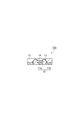
- FIG. 1 is a cross-sectional view showing a temporary protective film according to an embodiment.
- the temporary protective film 10 shown in FIG. 1 is composed of a support film 1 and an adhesive layer 2 provided on one side of the support film 1. Adhesive layers may be formed on both sides of the support film 1.
- FIG. 2 is also a cross-sectional view showing a temporary protective film according to an embodiment.
- the temporary protective film 10'in FIG. 2 has a support film 1, an adhesive layer 2 provided on one main surface of the support film 1, and a non-adhesive layer 3 provided on the other main surface of the support film 1. And have.
- These temporary protective films are used on the back surface of the lead frame (the side opposite to the surface on which the semiconductor element is mounted) in the sealing molding process of forming a sealing layer for sealing the semiconductor element mounted on the die pad of the lead frame.
- the adhesive layer 2 contains a thermoplastic resin and a low molecular weight additive.
- Thermoplastic resins include aromatic polyetherimides, aromatic polyetherimides, aromatic polyetheramides, aromatic polyamides, aromatic polyesters, aromatic polyimides, aromatic polyamideimides, aromatic polyethers, and aromatic polyesters. It may contain at least one selected from the group consisting of imides. From the viewpoint of heat resistance and adhesiveness, the thermoplastic resin may be at least one selected from the group consisting of aromatic polyetherimide, aromatic polyetherimide and aromatic polyetheramide, and may be aromatic. It may be a polyetheramide imide.
- Aromatic polyetheramidoimide is a polycondensate formed from an acid component containing an aromatic tricarboxylic acid or a reactive derivative thereof and an amine component containing an aromatic diamine, and is an aromatic tricarboxylic acid or an aromatic diamine. It can be a polycondensate containing at least one of the aromatic groups and a compound having an oxy group (—O—) that binds the aromatic groups to each other.
- the aromatic polyetherimide is a polycondensate formed from an acid component containing an aromatic tetracarboxylic acid or a reactive derivative thereof and an amine component containing an aromatic diamine, and is an aromatic tetracarboxylic acid or an aromatic diamine.
- At least one of them can be a polycondensate containing a plurality of aromatic groups and a compound having an oxy that binds the aromatic groups to each other.
- the aromatic polyether amide is a polycondensate formed from an acid component containing an aromatic dicarboxylic acid or a reactive derivative thereof and an amine component containing an aromatic diamine, and is one of the aromatic dicarboxylic acids or aromatic diamines. It can be a polycondensate containing at least one aromatic group and a compound having an oxy that binds the aromatic groups to each other.
- the reactive derivative of the carboxylic acid may be, for example, an acid anhydride or an acid chloride.
- aromatic polyetheramidoimide and the aromatic polyamideimide may contain a structural unit derived from trimellitic acid or a reactive derivative thereof.
- Aromatic polyimides and aromatic polyetherimides may contain building blocks derived from pyromellitic acids, polynuclear aromatic tetracarboxylic acids, or reactive derivatives thereof. Examples of polynuclear aromatic tetracarboxylic acids include bisphenol A bistrimeritate, and oxydiphthalic acid.
- Aromatic polyamides may contain constituent units derived from terephthalic acid, isophthalic acid, or reactive derivatives thereof.
- Aromatic polyetheramidoimides, aromatic polyetherimides and aromatic polyetheramides are, for example, 2,2-bis [4- (4-aminophenoxy) phenyl] propane, bis [4- (4-aminophenoxy). Oxy selected from phenyl] sulfone, 4,4'-diaminodiphenyl ether, bis [4- (4-aminophenoxy) phenyl] ether, and 2,2-bis [4- (4-aminophenoxy)] hexafluoropropane. It may contain a structural unit derived from an aromatic diamine having a group.
- Aromatic polyetheramidoimides, aromatic polyetherimides and aromatic polyetheramides are aromatic diamines having no oxy group (eg (eg, 4,4'-methylenebis (2-isopropylaniline)), siloxane diamines (eg, siloxanediamine). Derived from 1,3-bis (3-aminopropyl) tetramethyldisiloxane) and other diamines selected from ⁇ , ⁇ -diaminoalkanes (eg 1,12-diaminododecane, 1,6-diaminohexane) It may further include a structural unit.
- the ratio of the constituent units derived from the aromatic diamine having an oxy group is 40, based on the total amount of the constituent units derived from the diamine component. It may be -100 mol% or 50-97 mol%.
- the ratio of the constituent units derived from the aromatic diamine having an oxy group is 60 to 60, based on the total amount of the constituent units derived from the diamine component.
- the proportion of constituent units derived from siloxane diamine is 1-10 mol%, or 3-7 mol%, and the proportion of constituent units derived from ⁇ , ⁇ -diaminoalkane is It may be 10 to 30 mol% or 15 to 25 mol%.
- the ratio of the constituent units derived from the aromatic diamine having an oxy group is 90 to 90, based on the total amount of the constituent units derived from the diamine component.
- the proportion of the constituent units derived from the siloxane diamine may be 1 to 10 mol%, or 3 to 7 mol%.
- the ratio of the constituent units derived from the aromatic diamine having an oxy group is 40 to 40, based on the total amount of the constituent units derived from the diamine component. It may be 70 mol%, or 45-60 mol%, and the proportion of the structural unit derived from the aromatic diamine having no oxy group may be 30-60 mol%, or 40-55 mol%.
- the low molecular weight additive is a compound having a molecular weight of less than 1000, and is based on a change in the amount of oxygen on the surface of the copper plate when the paste obtained by attaching the adhesive layer to the surface of the copper plate is subjected to a predetermined heat treatment.
- the ratio of oxygen atoms X1 on the surface of the copper plate after heating at 180 ° C. for 1 hour is larger than the ratio of oxygen atoms X1 on the surface of the copper plate after heating at 180 ° C. for 1 hour.
- a low molecular weight additive having a small proportion X2 of oxygen atoms in the above is selected.
- the surface in contact with the adhesive layer of the copper plate is oxidized by heating at 180 ° C. for 1 hour to form a surface containing a large amount of oxygen atoms derived from copper oxide.
- the proportion of oxygen atoms on the surface of the copper plate decreases after heating at 400 ° C. for 2 minutes.
- the peelability from the lead frame after the heat treatment is improved.
- the decrease in the proportion of oxygen atoms suggests that at least part of the copper oxide is reduced by the reducing gas generated by the decomposition of the low molecular weight additives.
- the reducing gas may be hydrogen, carbon monoxide, or a hydrocarbon gas such as methane, propane, and butane.
- the temperature at which the reducing gas is generated may be 200 ° C. or higher, 250 ° C. or higher, 300 ° C. or higher, or 350 ° C. or higher, and 550 ° C. or higher. Hereinafter, it may be 500 ° C. or lower, 450 ° C. or lower, or 400 ° C. or lower.
- the surface of the copper plate used for measuring X1 and X2 may or may not be subjected to plasma irradiation treatment.
- the proportion of oxygen atoms on the surface of the copper plate can be measured, for example, by energy dispersive X-ray analysis (EDS) or X-ray photoelectron spectroscopy (XPS) on the surface exposed by peeling the adhesive layer.
- EDS energy dispersive X-ray analysis
- XPS X-ray photoelectron spectroscopy
- the proportion of oxygen atoms measured by the EDS method is 1.2 atomic% or less, 1.1 atomic% or less at the time after the heat treatment of heating at 180 ° C. for 1 hour and 400 ° C. for 2 minutes.
- the proportion of oxygen atoms measured by the EDS method is 0.5 atomic% or less, 0.4 atomic% or less, 0.3 atomic% or less, 0.2 atomic% or less, or 0. It may be 1 atomic% or less.
- the proportion of oxygen atoms measured by the EDS method is 0.5-5.0 atomic%, 0.5-4 at the time point after heating at 180 ° C. for 1 hour and before heating at 400 ° C. for 2 minutes. It may be .5 atomic%, 0.5-4.0 atomic%, 0.5-3.5 atomic%, 0.5-3.0 atomic%, or 0.5-1.0 atomic%. ..
- the low molecular weight additive may be an epoxy compound having one or more epoxy groups (or glycidyl ether groups), polyethylene glycol monoalkyl ether, polyethyleglycol dialkyl ether, or a combination thereof.
- epoxy compounds include sorbitol polyglycidyl ether and polyethylene glycol diglycidyl ether.
- Sorbitol polyglycidyl ether is a compound having a residue of sorbitol and two or more glycidyl ether groups bonded thereto, and may be a mixture of two or more components having different numbers of glycidyl ether groups.
- the epoxy equivalent of sorbitol polyglycidyl ether is, for example, 150-200 g / eq. It may be.
- Polyethylene glycol monoalkyl ether and polyethylene glycol dialkyl ether are ether compounds formed from one molecule of polyethylene glycol and one or two molecules of alkyl alcohol.
- the alkyl alcohol may have 6 to 24 carbon atoms.
- the alkyl alcohol may be a secondary alcohol.
- Examples of polyethylene glycol monoalkyl ethers and polyethylene glycol dialkyl ethers include polyoxyethylene (9) secondary alkyl (11-15 carbon atoms) ethers.
- the content of the low molecular weight additive is 5 to 30 parts by mass and 5 to 25 parts by mass with respect to 100 parts by mass of the thermoplastic resin from the viewpoint of peelability from the lead frame after receiving a thermal history at 400 ° C. It may be 5 to 20 parts by mass, 5 to 15 parts by mass, or 7 to 15 parts by mass. From the same viewpoint, the content of sorbitol polyglycidyl ether may be 5 to 20 parts by mass or 5 to 12 parts by mass with respect to the content of 100 parts by mass of the thermoplastic resin.
- the adhesive layer may further contain one or more coupling agents.
- the coupling agent may be a silane coupling agent.
- the silane coupling agent has the following formula (I): It may be a compound represented by.
- R 1 , R 2 and R 3 independently represent an alkoxy group having 1 to 3 carbon atoms, an alkyl group having 1 to 6 carbon atoms or an aryl group having 6 to 12 carbon atoms, and X is Indicates a group containing a reactive functional group.
- Examples of the alkoxy group having 1 to 3 carbon atoms as R 1 , R 2 or R 3 include a methoxy group, an ethoxy group, and a propoxy group.
- Examples of alkyl groups having 1 to 6 carbon atoms as R 1 , R 2 or R 3 include methyl group, ethyl group, propyl group, isopropyl group, butyl group, isobutyl group, tert-butyl group, pentyl group, and Hexyl groups can be mentioned.
- Examples of the aryl group having 6 to 12 carbon atoms as R 1 , R 2 or R 3 include a phenyl group, a tolyl group, a xsilyl group, and a naphthyl group.
- the reactive functional group of X may be, for example, an amino group, an isocyanate group, an amide group, or an epoxy group.
- X is the following formula (IIa), (IIb), (IIc), (IId), or (IIe): It may be a group represented by.
- R 4, R 5 and R 6 represents an alkyl group having 1 to 6 carbon atoms, an aryl group or a hydrogen atom having 6 to 12 carbon atoms. * Indicates the binding site with a carbon atom.
- R 4 , R 5 and R 6 are alkyl groups having 1 to 6 carbon atoms selected from methyl group, ethyl group, propyl group, isopropyl group, butyl group, isobutyl group, tert-butyl group, pentyl group and hexyl group.
- it may be an aryl group having 6 to 12 carbon atoms selected from a phenyl group, a tolyl group, a xsilyl group, and a naphthyl group.
- Examples of the silane coupling agent in which X is a group represented by the formula (IIa) are 3-aminopropyltrimethoxysilane, 3-aminopropylmethyldimethoxysilane, 3-aminopropyltriethoxysilane, and 3-aminopropyl.
- Methyldiethoxysilane 3-phenylaminopropyltrimethoxysilane, 3-phenylaminopropyltriethoxysilane, 3-phenylaminopropylmethyldimethoxysilane, 3-phenylaminopropylmethyldiethoxysilane, 3-methylaminopropyltrimethoxysilane , 3-Methylaminopropyltriethoxysilane, 3-ethylaminopropyltrimethoxysilane, and 3-ethylaminopropyltriethoxysilane.
- Examples of the silane coupling agent in which X is a group represented by the formula (IIb) are 3- (2-aminoethyl) -3-aminopropyltrimethoxysilane and 3- (2-aminoethyl) -3-.
- silane coupling agents in which X is a group represented by the formula (IIc) include 3-isocyanatopropyltrimethoxysilane, 3-isocyanatopropylmethyldimethoxysilane, 3-isocyanatopropyltriethoxysilane, and Examples thereof include 3-isocyanatopropylmethyldiethoxysilane.
- silane coupling agents in which X is a group represented by the formula (IId) are 3-ureidopropyltrimethoxysilane, 3-ureidopropylmethyldimethoxysilane, 3-ureidopropyltriethoxysilane, and 3-ureidopropyl.
- Examples of the silane coupling agent in which X is a group represented by the formula (IIe) are 3-glycidoxypropyltrimethoxysilane, 3-glycidoxypropylmethyldimethoxysilane, and 3-glycidoxypropyltriethoxy. Examples include silane and 3-glycidoxypropylmethyldiethoxysilane.
- the content of the coupling agent may be 1 to 40 parts by mass with respect to 100 parts by mass of the content of the thermoplastic resin.
- the content of the silane coupling agent is 1% by mass or more, the peelability from the lead frame after the heat treatment tends to be further improved.
- the content of the coupling agent is 40% by mass or less, gelation of the varnish for forming the adhesive layer 2 and decrease in viscosity are unlikely to occur, and a temporary protective film can be produced more easily.
- the content of the coupling agent is 1 to 35 parts by mass, 2 to 35 parts by mass, 3 to 30 parts by mass, and more than 5 parts by mass, 35 parts by mass with respect to 100 parts by mass of the thermoplastic resin content.
- it may be more than 5 parts by mass and 30% by mass or less, or more than 5 parts by mass and 20 parts by mass or less.
- the adhesive layer 2 may further contain a filler.
- fillers include ceramic powder, glass powder, silver powder, copper powder, resin particles, and rubber particles.
- the content of the filler may be 0 to 30 parts by mass, 1 to 30 parts by mass, or 5 to 15 parts by mass with respect to 100 parts by mass of the content of the thermoplastic resin.
- the total content of the thermoplastic resin, the low molecular weight additive, and the coupling agent in the adhesive layer 2 or the total content of the thermoplastic resin, the low molecular weight additive, the coupling agent, and the filler is the adhesive layer 2. It may be 90 to 100% by mass based on the mass of.
- the thickness of the adhesive layer 2 is 20 ⁇ m or less, 18 ⁇ m or less, 16 ⁇ m or less, 14 ⁇ m or less, 12 ⁇ m or less, 10 ⁇ m or less, 9 ⁇ m or less, or 8 ⁇ m or less from the viewpoint that the curl of the temporary protective film is more easily suppressed. good.
- the thickness of the adhesive layer 2 may be 1 ⁇ m or more, 2 ⁇ m or more, 3 ⁇ m or more, 4 ⁇ m or more, 5 ⁇ m or more, 6 ⁇ m or more, 7 ⁇ m or more, or 8 ⁇ m or more.
- the support film 1 includes, for example, aromatic polyimide, aromatic polyamide, aromatic polyamideimide, aromatic polysulfone, aromatic polyethersulfone, polyphenylene sulfide, aromatic polyetherketone, polyarylate, aromatic polyetheretherketone and polyethylene. It may be a film of at least one polymer selected from the group consisting of naphthalate.
- the support film 1 may be a film-like copper, aluminum, stainless steel or nickel. When the support film 1 is a polymer film, its surface is surface-treated by methods such as alkali treatment, chemical treatment such as silane coupling treatment, physical treatment such as sand mat treatment, plasma treatment, and corona treatment. You may.
- the thickness of the support film 1 may be, for example, 5 to 100 ⁇ m or 5 to 50 ⁇ m or less.
- the ratio T 2 / T 1 of the thickness T 2 of the adhesive layer to the thickness T 1 of the support film may be 0.5 or less, 0.3 or less, or 0.2 or less.
- the non-adhesive layer 3 is a resin layer that does not substantially have adhesiveness (or pressure-sensitive adhesiveness) to the lead frame at 0 to 270 ° C.
- the non-adhesive layer may be a resin layer that is hard to soften at a high temperature.
- a resin layer having a high glass transition temperature can function as a non-adhesive layer.
- the resin layer as the non-adhesive layer 3 contains a thermoplastic resin, a thermosetting resin (cured product), or a resin that is a combination thereof.
- the thermoplastic resin may have an amide group, an ester group, an imide group, an oxy group or a sulfonyl group.
- the thermosetting resin may be, for example, an epoxy resin, a phenol resin, or a bismaleimide resin. When the thermoplastic resin and the thermosetting resin are combined, the amount of the thermosetting resin may be 5 to 100 parts by mass or 20 to 70 parts by mass with respect to 100 parts by mass of the thermoplastic resin.
- the non-adhesive layer 3 may contain a filler (for example, ceramic powder, glass powder, silver powder, copper powder, resin particles, rubber particles), a coupling agent, or the like.
- the content of the filler in the non-adhesive layer 3 may be 1 to 30 parts by mass or 5 to 15 parts by mass with respect to 100 parts by mass of the resin content.
- the content of the coupling agent may be 1 to 20 parts by mass or 2 to 15 parts by mass with respect to 100 parts by mass of the resin content.
- the peel strength of the non-adhesive layer 3 with respect to the brass mold at 90 degrees may be less than 5 N / m or 1 N / m or less at 25 ° C. This peel strength is measured after the non-adhesive layer 3 is pressure-bonded to a brass mold at a temperature of 250 ° C. and a pressure of 8 MPa for 10 seconds.
- the thickness of the non-adhesive layer 3 may be, for example, 10 ⁇ m or less, 9 ⁇ m or less, 8 ⁇ m or less, or 7 ⁇ m or less.
- the thickness of the non-adhesive layer may be, for example, 1 ⁇ m or more, 2 ⁇ m or more, 3 ⁇ m or more, 4 ⁇ m or more, 5 ⁇ m or more, or 6 ⁇ m or more.
- the thickness of the non-adhesive layer is not particularly limited, but may be, for example, 1 to 10 ⁇ m or 1 to 8 ⁇ m.
- the temporary protective film can be produced, for example, by a method including a step of applying a varnish containing a thermoplastic resin, an epoxy compound and a solvent to a support film and removing the solvent from the coating film to form an adhesive layer.
- the non-adhesive layer can be formed in the same manner.
- a semiconductor package can be manufactured by using the temporary protective film according to the above-exemplified embodiment.
- the semiconductor package to be manufactured has, for example, a lead frame, a semiconductor element mounted on the lead frame, and a sealing layer for sealing the semiconductor element on the semiconductor element side of the lead frame, and the back surface of the lead frame is for external connection. It may be a Non Lead Type Package exposed to. Specific examples thereof include QFN (QuadFlat Non-led Package) and SON (Small Outline Non-read Package).
- FIG. 3 and 4 are cross-sectional views showing an embodiment of a method for manufacturing a semiconductor package.
- FIG. 5 is a cross-sectional view showing an embodiment of a semiconductor package obtained by the manufacturing methods of FIGS. 3 and 4.
- each process will be described with reference to each drawing as necessary.
- the method shown in FIGS. 3 and 4 is a step of attaching the temporary protective film 10 to the back surface, which is one surface of the lead frame 11 having the die pad 11a and the inner lead 11b, with the adhesive layer in contact with the lead frame 11.
- the step of mounting the semiconductor element 14 on the surface of the die pad 11a opposite to the temporary protective film 10, the step of providing the wire 12 connecting the semiconductor element 14 and the inner lead 11b, and the semiconductor element 14 and the wire 12 A step of forming a sealing layer 13 for sealing a seal to obtain a temporarily protected sealing molded body 20 having a lead frame 11, a semiconductor element 14, and a sealing layer 13, and temporary protection from the sealing molded body 20.
- a step of peeling the film 10 and a step of peeling the film 10 are provided in this order.
- the temporarily protected sealing molded body is composed of the sealing molded body 20 and the temporary protective film 10.
- the step of attaching the temporary protective film 10 to the lead frame 11 may include heating and pressurizing the temporary protective film 10 arranged on the lead frame 11.
- the heating temperature may be 150 ° C. or higher, 180 ° C. or higher, 200 ° C. or higher, or 400 ° C. or lower.
- the pressure may be 0.5 to 30 MPa, 1 to 20 MPa, or 3 to 15 MPa.
- the heating and pressurizing time may be 0.1 to 60 seconds, 1 to 30 seconds, or 3 to 20 seconds.
- the lead frame 11 may be formed of, for example, an iron-based alloy such as 42 alloy, copper, or a copper-based alloy.
- the lead frame 11 may have a molded body formed of copper or a copper-based alloy, and a coating layer of palladium, gold, silver, or the like that coats the surface thereof.
- the semiconductor element 14 is usually adhered to the die pad 11a via an adhesive (for example, silver paste). After adhering the semiconductor element 14 to the die pad 11a, reflow connection (CuClip connection or the like) may be performed under the conditions of a maximum temperature of 250 to 440 ° C. or 250 to 400 ° C. and 1 to 30 minutes.
- an adhesive for example, silver paste.
- the wire 12 is not particularly limited, but may be, for example, a gold wire, a copper wire, or a palladium-coated copper wire.
- the semiconductor element 14 and the inner lead 11b may be joined to the wire 12 by heating at 200 to 260 ° C. or 350 to 260 ° C. for 3 to 60 minutes using ultrasonic waves and pressing pressure.
- the sealing layer 13 is formed by sealing molding using a sealing material.
- a sealing molded body 20 having a plurality of semiconductor elements 14 and a sealing layer 13 that collectively seals them may be obtained. Since the temporary protective film 10 is provided during the sealing molding, it is possible to prevent the sealing material from wrapping around to the back surface side of the lead frame 11.
- the temperature during the formation of the sealing layer 13 (the temperature of the sealing material) may be 140 to 200 ° C. or 160 to 180 ° C.
- the pressure during the formation of the sealing layer may be 6 to 15 MPa or 7 to 10 MPa.
- the sealing molding time may be 1 to 5 minutes or 2 to 3 minutes.
- the formed sealing layer 13 may be heat-cured if necessary.
- the heating temperature for curing the sealing layer 13 may be 150 to 200 ° C. or 160 to 180 ° C.
- the heating time for curing the sealing layer 13 may be 4 to 7 hours, or 5 to 6 hours.
- a sealing material for example, an epoxy resin such as cresol novolac epoxy resin, phenol novolac epoxy resin, biphenyl diepoxy resin, or naphthol novolac epoxy resin may be contained.
- the sealing material may contain a filler, a flame-retardant substance such as a brom compound, a wax component, and the like.
- the temporary protective film 10 is peeled off from the lead frame 11 and the sealing layer 13 of the obtained sealing molded body 20.
- the temporary protective film 10 may be peeled off at any time before or after the curing of the sealing layer 13.
- the temperature at which the temporary protective film 10 is peeled from the sealed molded product 20 may be 0 to 250 ° C., 100 to 200 ° C., or 150 to 250 ° C.
- the solvent may be, for example, N-methyl-2-pyrrolidone, dimethylacetamide, diethylene glycol dimethyl ether, tetrahydrofuran, cyclohexanone, methyl ethyl ketone, or dimethylformamide.
- the sealing molded body 20 may be divided to obtain a plurality of semiconductor packages 100 of FIG. 5 each having one semiconductor element, if necessary. can. That is, when the lead frame 11 has a plurality of die pads 11a and the semiconductor element 14 is mounted on each of the plurality of die pads 11a, the manufacturing method according to one embodiment seals the temporary protective film 10 (or 10'). A step of dividing the sealing molded body 20 after peeling from the stop-molded body 20 to obtain a semiconductor package 100 having one die pad 11a and a semiconductor element 14 may be further provided.
- a semiconductor package may be manufactured by winding a long temporary protective film around a winding core and unwinding the temporary protective film from the obtained reel body.
- the reel body in this case has a winding core and a temporary protective film wound around the winding core according to the above-described embodiment.
- FIG. 6 is a perspective view showing an embodiment of the reel body.
- the reel body 30 shown in FIG. 6 includes a winding core 31, a temporary protective film 10 wound around the winding core 31, and a side plate 32.
- the width of the winding core 31 and the temporary protective film 10 (the length in the direction orthogonal to the winding direction) may be 0.001 cm or more, 0.005 cm or more, or 0.008 cm or more, and is 0.03 cm or less. It's okay.
- the width of the winding core 31 and the temporary protective film 10 (the length in the direction orthogonal to the winding direction) is, for example, 0.001 cm or more and 0.03 cm or less, 0.005 cm 0.03 cm or less, or 0.008 cm or more and 0.03 cm. It may be:
- the temporary protective film according to the above-described embodiment may be provided as a packaging body in which the reel body is housed in a packaging bag.
- FIG. 7 shows an embodiment of the package.
- the packaging body 50 includes a reel body 30 and a packaging bag 40 containing the reel body 30.
- the reel bodies 30 are usually individually housed in a packaging bag, but a plurality of (for example, 2 to 3) reel bodies 30 may be housed in one packaging bag 40.
- the packaging bag 40 may be formed of a resin film, or may be formed of a composite film which is a resin film having an aluminum layer. Specific examples of the packaging bag 40 include an aluminum-coated plastic bag and the like. Examples of the material of the resin film include plastics such as polyethylene, polyester, vinyl chloride, and polyethylene terephthalate.
- the reel body 30 may be housed in a packaging bag in a vacuum-packed state, for example.
- the package 50 is not limited to the vacuum-packed one.
- the packaging bag 40 may contain a desiccant together with the reel body 30.
- the desiccant include silica gel.
- the packaging body 50 may further have a cushioning material for wrapping the packaging bag 40 containing the reel body 30.
- the package 50 may be provided as a package housed in a package box.
- FIG. 8 shows an embodiment of the package.
- the package 70 includes a package 50 and a packaging box 60 containing the package 50.
- the packing box 60 contains one or more packaging bodies 50.
- the packing box 60 for example, corrugated cardboard can be used.
- the semiconductor device manufactured by using the temporary protective film according to one embodiment is excellent in terms of high density, small area, thinning, and the like.
- electronic devices such as mobile phones, smartphones, personal computers, and tablets. Can be suitably used for.
- a polyimide film having a chemically treated surface (thickness: 25 ⁇ m, manufactured by Ube Industries, Ltd., trade name: Upirex SGA) was used.
- the coating film on the support film is dried by heating at 100 ° C. for 10 minutes and at 200 ° C. for 10 minutes to form an adhesive layer having a thickness of 2 ⁇ m, and the temporary protection of Example 1 having the support film and the adhesive layer is formed. I got a film.
- Example 2 A varnish for forming an adhesive layer and a temporary protective film were obtained in the same manner as in Example 1 except that the amount of sorbitol polyglycidyl ether was changed to 10 parts by mass with respect to 100 parts by mass of aromatic polyether amidoimide. ..
- Example 3 Instead of sorbitol polyglycidyl ether, polyethylene glycol diglycidyl ether (manufactured by Kyoei Chemical Co., Ltd., trade name: Epolite 400E, epoxy equivalent: 264 to 290 g / eq.) Is used, and the amount is 100 mass of aromatic polyetheramidoimide.
- a varnish for forming an adhesive layer and a temporary protective film were obtained in the same manner as in Example 1 except that the portion was 10 parts by mass.
- Comparative Example 1 A varnish for forming an adhesive layer and a temporary protective film were obtained in the same manner as in Example 1 except that sorbitol polyglycidyl ether was not used.
- the temporary protective film was peeled off from each of the patches.
- the exposed copper plate surface was elementally analyzed by energy dispersive X-ray analysis (EDS) to determine the proportion of oxygen atoms (atomic%). The results are shown in Table 1.
- the copper plate A and the temporary protective film attached thereto were subjected to heat treatment at 180 ° C. for 1 hour, and subsequently at 400 ° C. for 2 minutes.
- the 90-degree peel strength between the adhesive layer and the copper plate A at 200 ° C. was measured under the condition of peeling speed: 300 mm / min.
- Table 2 shows the evaluation results of peel strength after pasting and after heat treatment.
- the temporary protective film of Example 1 exhibited an appropriate peel strength after application and a sufficiently reduced peel strength after heat treatment.
- Example 5 The same as in Example 4 except that the amount of polyoxyethylene (9) secondary alkyl (11 to 15 carbon atoms) ether was changed to 20 parts by mass with respect to 100 parts by mass of aromatic polyetheramideimide. A varnish for forming an adhesive layer and a temporary protective film were obtained.
Landscapes
- Chemical & Material Sciences (AREA)
- Organic Chemistry (AREA)
- Health & Medical Sciences (AREA)
- Chemical Kinetics & Catalysis (AREA)
- Medicinal Chemistry (AREA)
- Polymers & Plastics (AREA)
- Adhesives Or Adhesive Processes (AREA)
- Encapsulation Of And Coatings For Semiconductor Or Solid State Devices (AREA)
- Laminated Bodies (AREA)
Priority Applications (4)
| Application Number | Priority Date | Filing Date | Title |
|---|---|---|---|
| US17/995,408 US20230178385A1 (en) | 2020-04-06 | 2021-04-05 | Temporary protection film for semiconductor encapsulation, production method therefor, lead frame with temporary protection film, temporarily protected encapsulation object, and method for producing semiconductor package |
| KR1020227034878A KR102897541B1 (ko) | 2020-04-06 | 2021-04-05 | 반도체 밀봉 성형용 임시 보호 필름 및 그 제조 방법, 임시 보호 필름 부착 리드 프레임, 임시 보호된 밀봉 성형체, 및 반도체 패키지를 제조하는 방법 |
| JP2022514073A JP7687336B2 (ja) | 2020-04-06 | 2021-04-05 | 半導体封止成形用仮保護フィルム及びその製造方法、仮保護フィルム付きリードフレーム、仮保護された封止成形体、並びに、半導体パッケージを製造する方法 |
| CN202180024873.4A CN115335990B (zh) | 2020-04-06 | 2021-04-05 | 半导体密封成形用临时保护膜及其制造方法、带有临时保护膜的引线框、被临时保护的密封成形体以及制造半导体封装件的方法 |
Applications Claiming Priority (2)
| Application Number | Priority Date | Filing Date | Title |
|---|---|---|---|
| JP2020068397 | 2020-04-06 | ||
| JP2020-068397 | 2020-04-06 |
Publications (1)
| Publication Number | Publication Date |
|---|---|
| WO2021206069A1 true WO2021206069A1 (ja) | 2021-10-14 |
Family
ID=78023257
Family Applications (1)
| Application Number | Title | Priority Date | Filing Date |
|---|---|---|---|
| PCT/JP2021/014555 Ceased WO2021206069A1 (ja) | 2020-04-06 | 2021-04-05 | 半導体封止成形用仮保護フィルム及びその製造方法、仮保護フィルム付きリードフレーム、仮保護された封止成形体、並びに、半導体パッケージを製造する方法 |
Country Status (6)
| Country | Link |
|---|---|
| US (1) | US20230178385A1 (https=) |
| JP (1) | JP7687336B2 (https=) |
| KR (1) | KR102897541B1 (https=) |
| CN (1) | CN115335990B (https=) |
| TW (1) | TWI870576B (https=) |
| WO (1) | WO2021206069A1 (https=) |
Families Citing this family (1)
| Publication number | Priority date | Publication date | Assignee | Title |
|---|---|---|---|---|
| US12031013B2 (en) * | 2021-07-19 | 2024-07-09 | Momentive Performance Materials Inc. | Silane coupling agents to improve resin adhesion |
Citations (5)
| Publication number | Priority date | Publication date | Assignee | Title |
|---|---|---|---|---|
| JP2008103700A (ja) * | 2006-09-19 | 2008-05-01 | Hitachi Chem Co Ltd | 多層ダイボンドシート、半導体用接着フィルム付き半導体装置、半導体装置および半導体装置の製造方法 |
| JP2008277802A (ja) * | 2007-04-04 | 2008-11-13 | Hitachi Chem Co Ltd | 半導体用接着フィルム、半導体用接着フィルム付きリードフレーム及びこれらを用いた半導体装置 |
| WO2018207408A1 (ja) * | 2017-05-10 | 2018-11-15 | 日立化成株式会社 | 半導体封止成形用仮保護フィルム |
| WO2019176596A1 (ja) * | 2018-03-13 | 2019-09-19 | 日立化成株式会社 | 半導体封止成形用仮保護フィルム、仮保護フィルム付きリードフレーム、仮保護フィルム付き封止成形体、及び半導体装置を製造する方法 |
| WO2019176597A1 (ja) * | 2018-03-12 | 2019-09-19 | 日立化成株式会社 | 半導体封止成形用仮保護フィルム、仮保護フィルム付きリードフレーム、仮保護フィルム付き封止成形体及び半導体装置を製造する方法 |
Family Cites Families (7)
| Publication number | Priority date | Publication date | Assignee | Title |
|---|---|---|---|---|
| JPH05129473A (ja) | 1991-11-06 | 1993-05-25 | Sony Corp | 樹脂封止表面実装型半導体装置 |
| JPH1012773A (ja) | 1996-06-24 | 1998-01-16 | Matsushita Electron Corp | 樹脂封止型半導体装置およびその製造方法 |
| US6700185B1 (en) * | 1999-11-10 | 2004-03-02 | Hitachi Chemical Co., Ltd. | Adhesive film for semiconductor, lead frame and semiconductor device using the same, and method for manufacturing semiconductor device |
| TWI245791B (en) * | 2000-03-31 | 2005-12-21 | Hitachi Chemical Co Ltd | Adhesive films, and semiconductor devices using the same |
| CN1698200A (zh) * | 2003-02-19 | 2005-11-16 | 日立化成工业株式会社 | 半导体用粘着薄膜 ,使用该粘着薄膜的附有粘着薄膜金属板 ,附有该粘着薄膜的配线电路及半导体装置 ,以及半导体装置的制造方法 |
| JP6045773B2 (ja) * | 2009-11-26 | 2016-12-14 | 日立化成株式会社 | 接着シート及びその製造方法、並びに、半導体装置の製造方法及び半導体装置 |
| SG11201805612PA (en) * | 2016-02-08 | 2018-07-30 | Toray Industries | Resin Composition, Resin Layer, Permanent Adhesive, Adhesive For Temporary Bonding, Laminated Film, Processed Wafer, And Method For Manufacturing Electronic Component Or Semiconductor Device |
-
2021
- 2021-04-05 JP JP2022514073A patent/JP7687336B2/ja active Active
- 2021-04-05 CN CN202180024873.4A patent/CN115335990B/zh active Active
- 2021-04-05 US US17/995,408 patent/US20230178385A1/en active Pending
- 2021-04-05 KR KR1020227034878A patent/KR102897541B1/ko active Active
- 2021-04-05 WO PCT/JP2021/014555 patent/WO2021206069A1/ja not_active Ceased
- 2021-04-06 TW TW110112335A patent/TWI870576B/zh active
Patent Citations (5)
| Publication number | Priority date | Publication date | Assignee | Title |
|---|---|---|---|---|
| JP2008103700A (ja) * | 2006-09-19 | 2008-05-01 | Hitachi Chem Co Ltd | 多層ダイボンドシート、半導体用接着フィルム付き半導体装置、半導体装置および半導体装置の製造方法 |
| JP2008277802A (ja) * | 2007-04-04 | 2008-11-13 | Hitachi Chem Co Ltd | 半導体用接着フィルム、半導体用接着フィルム付きリードフレーム及びこれらを用いた半導体装置 |
| WO2018207408A1 (ja) * | 2017-05-10 | 2018-11-15 | 日立化成株式会社 | 半導体封止成形用仮保護フィルム |
| WO2019176597A1 (ja) * | 2018-03-12 | 2019-09-19 | 日立化成株式会社 | 半導体封止成形用仮保護フィルム、仮保護フィルム付きリードフレーム、仮保護フィルム付き封止成形体及び半導体装置を製造する方法 |
| WO2019176596A1 (ja) * | 2018-03-13 | 2019-09-19 | 日立化成株式会社 | 半導体封止成形用仮保護フィルム、仮保護フィルム付きリードフレーム、仮保護フィルム付き封止成形体、及び半導体装置を製造する方法 |
Also Published As
| Publication number | Publication date |
|---|---|
| TWI870576B (zh) | 2025-01-21 |
| US20230178385A1 (en) | 2023-06-08 |
| KR102897541B1 (ko) | 2025-12-08 |
| JP7687336B2 (ja) | 2025-06-03 |
| CN115335990B (zh) | 2025-07-11 |
| KR20220160008A (ko) | 2022-12-05 |
| JPWO2021206069A1 (https=) | 2021-10-14 |
| CN115335990A (zh) | 2022-11-11 |
| TW202146608A (zh) | 2021-12-16 |
Similar Documents
| Publication | Publication Date | Title |
|---|---|---|
| US11682564B2 (en) | Temporary protective film for semiconductor encapsulation molding, lead frame provided with temporary protective film, encapsulated molded body provided with temporary protective film, and method for manufacturing semiconductor device | |
| JP6747621B2 (ja) | 半導体封止成形用仮保護フィルム、仮保護フィルム付きリードフレーム、仮保護フィルム付き封止成形体及び半導体装置を製造する方法 | |
| WO2021206069A1 (ja) | 半導体封止成形用仮保護フィルム及びその製造方法、仮保護フィルム付きリードフレーム、仮保護された封止成形体、並びに、半導体パッケージを製造する方法 | |
| WO2020255975A1 (ja) | 半導体封止成形用仮保護フィルム、仮保護フィルム付きリードフレーム、仮保護フィルム付き封止成形体、及び半導体装置を製造する方法 | |
| JP7447647B2 (ja) | 半導体封止成形用仮保護フィルム及びその製造方法、仮保護フィルム付きリードフレーム、封止成形体、並びに、半導体パッケージを製造する方法 | |
| JP6744004B1 (ja) | 仮保護フィルム、リール体、包装体、梱包体、仮保護体、及び、半導体装置を製造する方法 | |
| US12435248B2 (en) | Temporary protective film for semiconductor encapsulation molding, lead frame provided with temporary protective film, encapsulation molded body, and method for manufacturing semiconductor package | |
| WO2025192663A1 (ja) | 半導体封止成形用仮保護フィルム及びその製造方法、仮保護フィルム付きリードフレーム、仮保護された封止成形体、並びに、半導体パッケージを製造する方法 |
Legal Events
| Date | Code | Title | Description |
|---|---|---|---|
| 121 | Ep: the epo has been informed by wipo that ep was designated in this application |
Ref document number: 21785005 Country of ref document: EP Kind code of ref document: A1 |
|
| ENP | Entry into the national phase |
Ref document number: 2022514073 Country of ref document: JP Kind code of ref document: A |
|
| ENP | Entry into the national phase |
Ref document number: 20227034878 Country of ref document: KR Kind code of ref document: A |
|
| NENP | Non-entry into the national phase |
Ref country code: DE |
|
| 122 | Ep: pct application non-entry in european phase |
Ref document number: 21785005 Country of ref document: EP Kind code of ref document: A1 |
|
| WWG | Wipo information: grant in national office |
Ref document number: 202180024873.4 Country of ref document: CN |