WO2021200770A1 - バックライトユニットおよび画像表示装置 - Google Patents
バックライトユニットおよび画像表示装置 Download PDFInfo
- Publication number
- WO2021200770A1 WO2021200770A1 PCT/JP2021/013165 JP2021013165W WO2021200770A1 WO 2021200770 A1 WO2021200770 A1 WO 2021200770A1 JP 2021013165 W JP2021013165 W JP 2021013165W WO 2021200770 A1 WO2021200770 A1 WO 2021200770A1
- Authority
- WO
- WIPO (PCT)
- Prior art keywords
- light
- light source
- shielding
- guide plate
- backlight unit
- Prior art date
- Legal status (The legal status is an assumption and is not a legal conclusion. Google has not performed a legal analysis and makes no representation as to the accuracy of the status listed.)
- Ceased
Links
Images
Classifications
-
- G—PHYSICS
- G02—OPTICS
- G02B—OPTICAL ELEMENTS, SYSTEMS OR APPARATUS
- G02B6/00—Light guides; Structural details of arrangements comprising light guides and other optical elements, e.g. couplings
- G02B6/0001—Light guides; Structural details of arrangements comprising light guides and other optical elements, e.g. couplings specially adapted for lighting devices or systems
- G02B6/0011—Light guides; Structural details of arrangements comprising light guides and other optical elements, e.g. couplings specially adapted for lighting devices or systems the light guides being planar or of plate-like form
- G02B6/0081—Mechanical or electrical aspects of the light guide and light source in the lighting device peculiar to the adaptation to planar light guides, e.g. concerning packaging
- G02B6/0086—Positioning aspects
- G02B6/0091—Positioning aspects of the light source relative to the light guide
-
- F—MECHANICAL ENGINEERING; LIGHTING; HEATING; WEAPONS; BLASTING
- F21—LIGHTING
- F21K—NON-ELECTRIC LIGHT SOURCES USING LUMINESCENCE; LIGHT SOURCES USING ELECTROCHEMILUMINESCENCE; LIGHT SOURCES USING CHARGES OF COMBUSTIBLE MATERIAL; LIGHT SOURCES USING SEMICONDUCTOR DEVICES AS LIGHT-GENERATING ELEMENTS; LIGHT SOURCES NOT OTHERWISE PROVIDED FOR
- F21K9/00—Light sources using semiconductor devices as light-generating elements, e.g. using light-emitting diodes [LED] or lasers
- F21K9/60—Optical arrangements integrated in the light source, e.g. for improving the colour rendering index or the light extraction
- F21K9/61—Optical arrangements integrated in the light source, e.g. for improving the colour rendering index or the light extraction using light guides
-
- F—MECHANICAL ENGINEERING; LIGHTING; HEATING; WEAPONS; BLASTING
- F21—LIGHTING
- F21S—NON-PORTABLE LIGHTING DEVICES; SYSTEMS THEREOF; VEHICLE LIGHTING DEVICES SPECIALLY ADAPTED FOR VEHICLE EXTERIORS
- F21S2/00—Systems of lighting devices, not provided for in main groups F21S4/00 - F21S10/00 or F21S19/00, e.g. of modular construction
-
- G—PHYSICS
- G02—OPTICS
- G02B—OPTICAL ELEMENTS, SYSTEMS OR APPARATUS
- G02B6/00—Light guides; Structural details of arrangements comprising light guides and other optical elements, e.g. couplings
- G02B6/0001—Light guides; Structural details of arrangements comprising light guides and other optical elements, e.g. couplings specially adapted for lighting devices or systems
-
- G—PHYSICS
- G02—OPTICS
- G02B—OPTICAL ELEMENTS, SYSTEMS OR APPARATUS
- G02B6/00—Light guides; Structural details of arrangements comprising light guides and other optical elements, e.g. couplings
- G02B6/0001—Light guides; Structural details of arrangements comprising light guides and other optical elements, e.g. couplings specially adapted for lighting devices or systems
- G02B6/0011—Light guides; Structural details of arrangements comprising light guides and other optical elements, e.g. couplings specially adapted for lighting devices or systems the light guides being planar or of plate-like form
- G02B6/0033—Means for improving the coupling-out of light from the light guide
- G02B6/005—Means for improving the coupling-out of light from the light guide provided by one optical element, or plurality thereof, placed on the light output side of the light guide
- G02B6/0055—Reflecting element, sheet or layer
-
- G—PHYSICS
- G02—OPTICS
- G02B—OPTICAL ELEMENTS, SYSTEMS OR APPARATUS
- G02B6/00—Light guides; Structural details of arrangements comprising light guides and other optical elements, e.g. couplings
- G02B6/0001—Light guides; Structural details of arrangements comprising light guides and other optical elements, e.g. couplings specially adapted for lighting devices or systems
- G02B6/0011—Light guides; Structural details of arrangements comprising light guides and other optical elements, e.g. couplings specially adapted for lighting devices or systems the light guides being planar or of plate-like form
- G02B6/0081—Mechanical or electrical aspects of the light guide and light source in the lighting device peculiar to the adaptation to planar light guides, e.g. concerning packaging
- G02B6/0086—Positioning aspects
- G02B6/0088—Positioning aspects of the light guide or other optical sheets in the package
-
- F—MECHANICAL ENGINEERING; LIGHTING; HEATING; WEAPONS; BLASTING
- F21—LIGHTING
- F21V—FUNCTIONAL FEATURES OR DETAILS OF LIGHTING DEVICES OR SYSTEMS THEREOF; STRUCTURAL COMBINATIONS OF LIGHTING DEVICES WITH OTHER ARTICLES, NOT OTHERWISE PROVIDED FOR
- F21V2200/00—Use of light guides, e.g. fibre optic devices, in lighting devices or systems
-
- F—MECHANICAL ENGINEERING; LIGHTING; HEATING; WEAPONS; BLASTING
- F21—LIGHTING
- F21Y—INDEXING SCHEME ASSOCIATED WITH SUBCLASSES F21K, F21L, F21S and F21V, RELATING TO THE FORM OR THE KIND OF THE LIGHT SOURCES OR OF THE COLOUR OF THE LIGHT EMITTED
- F21Y2115/00—Light-generating elements of semiconductor light sources
- F21Y2115/10—Light-emitting diodes [LED]
-
- G—PHYSICS
- G02—OPTICS
- G02F—OPTICAL DEVICES OR ARRANGEMENTS FOR THE CONTROL OF LIGHT BY MODIFICATION OF THE OPTICAL PROPERTIES OF THE MEDIA OF THE ELEMENTS INVOLVED THEREIN; NON-LINEAR OPTICS; FREQUENCY-CHANGING OF LIGHT; OPTICAL LOGIC ELEMENTS; OPTICAL ANALOGUE/DIGITAL CONVERTERS
- G02F1/00—Devices or arrangements for the control of the intensity, colour, phase, polarisation or direction of light arriving from an independent light source, e.g. switching, gating or modulating; Non-linear optics
- G02F1/01—Devices or arrangements for the control of the intensity, colour, phase, polarisation or direction of light arriving from an independent light source, e.g. switching, gating or modulating; Non-linear optics for the control of the intensity, phase, polarisation or colour
- G02F1/13—Devices or arrangements for the control of the intensity, colour, phase, polarisation or direction of light arriving from an independent light source, e.g. switching, gating or modulating; Non-linear optics for the control of the intensity, phase, polarisation or colour based on liquid crystals, e.g. single liquid crystal display cells
- G02F1/133—Constructional arrangements; Operation of liquid crystal cells; Circuit arrangements
- G02F1/1333—Constructional arrangements; Manufacturing methods
- G02F1/1335—Structural association of cells with optical devices, e.g. polarisers or reflectors
- G02F1/1336—Illuminating devices
- G02F1/133615—Edge-illuminating devices, i.e. illuminating from the side
-
- G—PHYSICS
- G02—OPTICS
- G02F—OPTICAL DEVICES OR ARRANGEMENTS FOR THE CONTROL OF LIGHT BY MODIFICATION OF THE OPTICAL PROPERTIES OF THE MEDIA OF THE ELEMENTS INVOLVED THEREIN; NON-LINEAR OPTICS; FREQUENCY-CHANGING OF LIGHT; OPTICAL LOGIC ELEMENTS; OPTICAL ANALOGUE/DIGITAL CONVERTERS
- G02F2202/00—Materials and properties
- G02F2202/28—Adhesive materials or arrangements
Definitions
- the present invention relates to a backlight unit.
- a technique of laminating a light guide plate and a reflector via a low refractive index layer is known. According to such a technique, it is reported that the light utilization efficiency is higher than that in the case of simply laminating with only an adhesive by using a low refractive index layer. However, even with such a technique, the light is emitted near the incident surface of the light from the light source, and the uniformity of the brightness may not be sufficient.
- the present invention has been made to solve the above-mentioned conventional problems, and its main purpose is to provide a backlight unit having excellent brightness uniformity.
- the backlight unit includes a light source; a light guide plate arranged facing the light source and having an end surface on which light from the light source is incident and an exit surface on which the incident light is emitted; A reflector attached to the back side of the light guide plate via a double-sided adhesive film; a light source having a front surface portion and a back surface portion, and a housing for accommodating the light source plate and the reflector;
- the double-sided pressure-sensitive adhesive film has a first pressure-sensitive adhesive layer, a low refractive index layer, and a second pressure-sensitive adhesive layer in this order from the light guide plate side.
- the light from the light source is not incident between the low refractive index layer and the reflecting plate, or the light incident from the light source between the low refractive index layer and the reflecting plate is incident on the light guide plate. It is configured so that it does not emit light from the exit surface.
- the light source side end face of the double-sided adhesive film and the light source side end face of the reflector are substantially flush with each other.
- the backlight unit is provided with a light-shielding printing portion in the vicinity of the light source-side end portion of the reflector.
- the backlight unit is selected from a light-shielding tape, a solidified or cured product of a coating film of a light-shielding resin solution, and a light-shielding molded product on the light source-side end surface of the low refractive index layer.
- a light-shielding portion is provided.
- the reflector has an extension portion that extends closer to the light source than the double-sided adhesive film, and the extension portion is a solidified or cured film of a light-shielding tape or a light-shielding resin solution.
- a light-shielding portion selected from an object and a light-shielding molded body is provided.
- the low refractive index layer and the reflector have an extension portion extending toward the light source side with respect to the light guide plate.
- a reflective layer is further provided on the extending portion of the low refractive index layer.
- the backlight unit is defined at the light source side end of the light guide plate so that the end faces of the double-sided adhesive film and the reflector are separated from the light source by the end face of the light guide plate.
- a gap portion is formed, and the gap portion is provided with a light-shielding tape, a solidified or cured product of a coating film of a light-shielding resin solution, and a light-shielding portion selected from a light-shielding molded product.
- the backlight unit is defined at the light source side end of the light guide plate so that the end faces of the double-sided adhesive film and the reflector are separated from the light source by the end face of the light guide plate.
- a gap portion is formed, and a protruding portion matching the shape of the gap portion is provided at a position corresponding to the gap portion on the back surface portion of the housing.
- the light source is an LED light source.
- an image display device is provided. This image display device includes the backlight unit and an image display panel arranged on the exit surface side of the light guide plate.
- a backlight unit including a light guide plate and a reflector bonded with a double-sided adhesive film having a low refractive index layer
- light is not incident from the light source side end surface of the low refractive index layer.
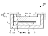
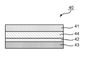
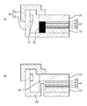
- FIG. 1 It is the schematic sectional drawing of the backlight unit by one Embodiment of this invention. It is a schematic cross-sectional view of the double-sided adhesive film which can be used for the backlight unit of FIG.
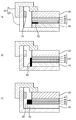
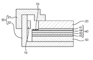
- Each of (a) to (c) is a schematic partial cross-sectional view illustrating a specific example of a light-shielding configuration according to an embodiment of the present invention. It is a schematic partial sectional view explaining another specific example of the light-shielding structure in embodiment of this invention.
- Each of (a) and (b) is a schematic partial cross-sectional view illustrating still another specific example of the light-shielding configuration according to the embodiment of the present invention.
- FIG. 1 is a schematic cross-sectional view of the backlight unit according to one embodiment of the present invention
- FIG. 2 is a schematic cross-sectional view of the double-sided adhesive film used in the backlight unit of FIG. .
- the backlight unit 100 of the illustrated example includes a light source 10, a light guide plate 20, a housing 30, a double-sided adhesive film 40, and a reflector 50.
- the back surface side of the light guide plate 20 and the reflector 50 are bonded to each other via a double-sided adhesive film 40.
- the housing 30 has a front surface portion 31 and a back surface portion 32, and houses a light source 10, a light guide plate 20, and a reflector 50.
- the back surface portion 32 has a box shape with an upper side (front side) open, and the front surface portion 31 projects inward from the back surface portion at a pair of opposite end portions of the back surface portion 32.
- the front surface portion 31 and the back surface portion 32 are typically fixed and integrated.
- the housing 30 can be fitted with the light guide plate 20 and the reflector 50.
- any suitable optical member (not shown) can be placed (horizontally) on the stepped portion (inwardly projecting portion) of the front surface portion. Examples of the optical member include a diffusion sheet and a prism sheet. A plurality of diffusion sheets and / or prism sheets may be placed.
- the housing 30 in the illustrated example is a back surface portion of the housing that accommodates the entire image display device.
- the light source 10 is arranged on one end side of the light guide plate 20 so as to face the end surface 20a of the light guide plate. Therefore, the backlight unit is typically an edge light type.
- the light source 10 is typically surrounded by a reflector (not shown). Any suitable configuration can be adopted as the light source. Specific examples include a light emitting diode (LED: Light Emitting Dimension), a cold cathode fluorescent lamp (CCFL: Cold Fluorescent Lamp), an external electrode fluorescent lamp (EEFL: External Electrolectrode Fluorescent Lamp), and a hot cathode fluorescent lamp (HCFL). ).
- LED Light Emitting Dimension
- CCFL Cold Fluorescent Lamp
- EEFL External Electrolectrode Fluorescent Lamp
- HCFL hot cathode fluorescent lamp
- an LED light source may be used.
- the LED light source can be typically configured by arranging LEDs (point light sources) in a row.
- the light guide plate 20 has an end surface 20a on which the light from the light source is incident and an exit surface 20b on which the incident light is emitted.
- the light guide plate 20 has an end face 20a arranged so as to face the light source 10. More specifically, the light guide plate 20 guides the light incident on the end face 20a from the light source 10 to the end side facing the end face 20a while receiving an internal reflection action or the like, and gradually emits the light in the light guide process. It emits light from the exit surface 20b.
- An emission pattern is typically provided on the emission surface 20b. Examples of the emission pattern include a concave-convex shape. Further, a light extraction pattern is typically provided on the surface of the light guide plate opposite to the exit surface. Examples of the light extraction pattern include white dots.
- any suitable configuration can be adopted as the light guide plate.
- the material constituting the light guide plate any suitable material can be used as long as the light emitted from the light source can be efficiently guided.
- the material constituting the light guide plate include an acrylic resin such as polymethylmethacrylate (PMMA), a polycarbonate (PC) resin, a polyethylene terephthalate (PET) resin, and a styrene resin.
- PMMA polymethylmethacrylate
- PC polycarbonate
- PET polyethylene terephthalate
- styrene resin styrene resin.
- the back side of the light guide plate 20 is attached to the flexible printed circuit board for a light source via any suitable means (for example, adhesive tape).
- the double-sided adhesive film 40 has a first adhesive layer 41, a low refractive index layer 42, and a second adhesive layer 43 from the light guide plate 20 side.
- the base material 44 is provided between the first pressure-sensitive adhesive layer 41 and the low refractive index layer 42.
- the low refractive index layer 42 is formed on the surface of the base material 44, and the first pressure-sensitive adhesive layer 41 and the second pressure-sensitive adhesive layer 43 are formed on both sides of the laminate of the base material 44 and the low-refractive index layer 42. Can be placed.
- the reflector 50 any suitable reflector can be used.
- the reflector may be a specular reflector or a diffuse reflector.
- Specific examples of the reflective plate include vapor deposition of aluminum, silver, etc. on a base material such as a highly reflective resin sheet (for example, acrylic plate), a thin metal plate such as aluminum or stainless steel, or a metal foil or a resin film such as polyester. Examples thereof include a sheet, a laminate of a base material such as a resin film such as polyester and a metal foil such as aluminum, and a resin film having pores (voids) formed inside.
- the backlight unit 100 prevents the light from the light source from entering between the low refraction layer 42 and the reflector 50, or prevents the light from the light source from entering the low refraction layer 42 and the reflector 50.
- the light incident between them is configured so as not to be emitted from the exit surface 20b of the light guide plate 20.
- a “light-shielding configuration” By providing the light-shielding configuration, light leakage in the vicinity of the incident surface of the light from the light source can be remarkably suppressed, and as a result, a backlight unit having excellent brightness uniformity can be realized.
- FIGS. 3 (a) to 3 (c) are schematic partial cross-sectional views for explaining a specific example of the light-shielding configuration.
- the light source side end face of the double-sided adhesive film 40 and the light source side end face of the reflector 50 are substantially flush with each other (that is, the end faces are at the same position). be).
- a light-shielding printing unit 52 is provided near the light source side end of the reflector 50.
- the light-shielding printing layer is typically a solid colored layer, preferably a black colored layer.
- the light-shielding printing layer has a total light transmittance of preferably 0.01% or less, more preferably 0.008% or less at a thickness of 3 ⁇ m to 5 ⁇ m. The smaller the total light transmittance of the light-shielding printing layer, the more preferable, and the lower limit thereof can be, for example, 0.001%. If the total light transmittance of the light-shielding print layer is within such a range, an excellent light-shielding function can be realized.
- the thickness of the light-shielding printing layer is preferably 3 ⁇ m to 5 ⁇ m. With such a thickness, it is easy to realize a desired total light transmittance (as a result, a light-shielding function) by appropriately selecting a constituent material.
- the light-shielding printing layer can be formed by any suitable printing method using any suitable ink or paint. Specific examples of the printing method include gravure printing, offset printing, silk screen printing, and transfer printing from a transfer sheet.
- the ink or paint used typically includes a binder, a colorant, a solvent and any suitable additive that may be used as needed.
- the binder include chlorinated polyolefins (for example, chlorinated polyethylene and chlorinated polypropylene), polyester resins, urethane resins, acrylic resins, vinyl acetate resins, vinyl chloride-vinyl acetate copolymers, and cellulose resins. ..
- the binder resin may be used alone or in combination of two or more.
- the binder resin is a thermopolymerizable resin.
- the binder resin is an acrylic resin, preferably an acrylic resin containing a polyfunctional monomer (for example, pentaerythritol triacrylate) as a copolymerization component.
- a polyfunctional monomer for example, pentaerythritol triacrylate
- any suitable colorant can be used depending on the purpose.
- colorants include inorganic pigments such as titanium white, zinc flower, carbon black, iron black, petal handle, chrome vermilion, ultramarine blue, cobalt blue, yellow lead, and titanium yellow; phthalocyanine blue, induslen blue, and iso.
- Organic pigments or dyes such as indolinone yellow, benzidine yellow, quinacridone red, polyazo red, perylene red, aniline black; metal pigments composed of scaly foil pieces such as aluminum and brass; scales such as titanium dioxide coated mica and basic lead carbonate. Examples thereof include pearl luster pigments (pearl pigments) composed of shaped foil pieces.
- a black colored layer carbon black, iron black, and aniline black are preferably used.
- a colorant in combination. This is because it can absorb visible light over a wide range and evenly to form a non-colored (ie, black) colored layer.
- azo compounds and / or quinone compounds can be used.
- the colorant comprises carbon black as the main component and other colorants (eg, azo compounds and / or quinone compounds). According to such a configuration, it is possible to form a colored layer that is not colored and has excellent stability over time.
- the colorant When forming a black colored layer, the colorant can be used in a ratio of preferably 50 parts by weight to 200 parts by weight with respect to 100 parts by weight of the binder resin.
- the content ratio of carbon black in the colorant is preferably 80% to 100%.
- a light shielding portion 60 is provided on the light source side end surface of the low refractive index layer 42.
- the light-shielding portion 60 may be optically provided on the light source-side end surface of the low-refractive-index layer 42, but is substantially the double-sided adhesive film 40 (or the double-sided adhesive film excluding the first adhesive layer). It may be provided on the light source side end face, or on the light source side end face of the double-sided adhesive film 40 (or the double-sided pressure-sensitive adhesive film excluding the first pressure-sensitive adhesive layer) and the light source side end face of the reflector 50.
- Examples of the light-shielding portion 60 include a light-shielding tape, a solidified or cured product of a coating film of a light-shielding resin solution, and a light-shielding molded product.
- the light-shielding tape typically has a light-shielding base material and an adhesive layer or an adhesive layer.
- the light-shielding base material is typically a resin film containing a colorant. As the colorant, the colorant described with respect to the example of FIG. 3A can be used.
- the light-shielding base material is typically a black tape.
- the solidified or cured product of the coating film of the light-shielding resin solution is the same as the above-mentioned light-shielding printing layer in one embodiment.
- the light-shielding resin solution can be, for example, an ink or paint that forms the above-mentioned light-shielding printing layer.
- the light-shielding resin solution may contain any suitable thermoplastic resin as a binder. Due to the formation position, the light-shielding portion is formed by applying and solidifying or curing such an ink or paint rather than printing it.
- the light-shielding molded product is a light-shielding resin molded product.
- the light-shielding resin typically contains a base resin (binder) and a colorant.
- the light-shielding molded product can be, for example, a box-shaped product or a plate-shaped product.
- the total light transmittance when the thickness of the light-shielding portion is 3 ⁇ m to 5 ⁇ m is preferably 0.01% or less, more preferably 0.008% or less, as described above.
- the smaller the total light transmittance of the light-shielding portion, the more preferable, and the lower limit thereof can be, for example, 0.001%.
- the reflector 50 has an extending portion 54 extending toward the light source side of the double-sided adhesive film 40, and the extending portion 54 is provided with a light-shielding portion 60.
- FIG. 4 is a schematic partial cross-sectional view illustrating another specific example of the shading configuration.
- the low refractive index layer 42 and the reflector 50 have an extending portion extending toward the light source side with respect to the light guide plate 20.
- the low refractive index layer 42 may have an extending portion, but substantially (structurally) in order to support the extending portion of the low refractive index layer 42 as shown in the illustrated example.
- the base material 44, the second pressure-sensitive adhesive layer 43, and the reflector 50 may also have an extension.
- the extension preferably extends to a position corresponding to the exit surface of the light source (eg, LED). More preferably, as shown in the figure, the extending portion is provided with a reflective layer 70.
- the light emitted from the light source can be reflected by the low refractive index layer, so that it is possible to prevent the light from entering the pressure-sensitive adhesive layer and the base material.
- the details of the reflective layer 70 will be described below.
- a reflective layer 70 is preferably further provided on the extending portion of the low refractive index layer 42 (the first pressure-sensitive adhesive layer 41 in the drawing) as described above.
- the reflective layer may be, for example, the reflector described in Section A above with respect to the reflector 50, or a metal-deposited film.
- the reflectance of the reflective layer is preferably 80% to 100%, more preferably 95% to 100%. If the first pressure-sensitive adhesive layer 41 has an extending portion as shown in the illustrated example, the reflective layer 70 can be attached to the first pressure-sensitive adhesive layer 41. If the first pressure-sensitive adhesive layer 41 does not have an extension, the reflective layer 70 is attached to the extension of the low index layer via any suitable pressure-sensitive adhesive layer or adhesive layer. It may be formed directly on the extending portion of the low refractive index layer.
- 5 (a) and 5 (b) are schematic partial cross-sectional views for explaining still another specific example of the light-shielding configuration.
- the end faces of the double-sided adhesive film 40 and the reflector 50 are located farther from the light source 10 than the end faces of the light guide plate 20.
- a gap portion is formed on the back surface side of the light source side end portion of the light guide plate 20.
- a light-shielding portion 60 is provided in the gap portion.
- Examples of the light-shielding portion 60 include a light-shielding tape, a solidified or cured product of a coating film of a light-shielding resin solution, and a light-shielding molded product.
- the light-shielding molded product preferably has a shape suitable for the shape of the void portion. With such a configuration, it is possible to prevent the light guide plate 20 from being tilted, misaligned, and the like.
- a gap portion is formed on the back side of the light source side end portion of the light guide plate 20.
- the protruding portion 36 is provided at a position corresponding to the gap portion of the back surface portion 32 of the housing 31. Since the housing has a light-shielding property, the protrusion 36 can function as a light-shielding configuration.
- the protrusion 36 preferably has a shape that matches the shape of the gap, and can substantially support the light guide plate.
- Double-sided adhesive film C-1 Outline of Double-sided Adhesive Film
- the double-sided adhesive film 40 has a first pressure-sensitive adhesive layer 41, a low refractive index layer 42, and a base material 44 and a second base material 44, if necessary, from the light guide plate 20 side. It has a pressure-sensitive adhesive layer 43.
- the base material 44 can be typically composed of a resin (preferably a transparent resin) film or a plate-like material.
- resins include thermoplastic resins and reactive resins (for example, ionizing radiation curable resins).
- thermoplastic resin include (meth) acrylic resins such as polymethyl methacrylate (PMMA) and polyacrylonitrile, polycarbonate (PC) resins, polyester resins such as PET, and cellulose-based resins such as triacetyl cellulose (TAC). Examples thereof include resins, cyclic polyolefin resins, and styrene resins.
- the ionizing radiation curable resin include epoxy acrylate resins and urethane acrylate resins. These resins may be used alone or in combination of two or more.
- the thickness of the base material is, for example, 10 ⁇ m to 100 ⁇ m, preferably 10 ⁇ m to 50 ⁇ m.
- the refractive index of the base material is preferably 1.47 or more, more preferably 1.47 to 1.60, and further preferably 1.47 to 1.55. Within such a range, the light can be guided to the image display cell without adversely affecting the light extracted from the light guide plate.
- the low refractive index layer 42 typically has voids inside.
- the porosity of the low refractive index layer is, for example, 40% or more, typically 50% or more, preferably 70% or more, and more preferably 80% or more. On the other hand, the porosity is, for example, 90% or less, preferably 85% or less. When the porosity is within the above range, the refractive index of the low refractive index layer can be set within an appropriate range.
- the porosity is a value obtained by calculating the porosity from the value of the refractive index measured by an ellipsometer from Lorentz-Lorenz's formula (Lorentz-Lorenz's formula).
- the refractive index of the low refractive index layer is preferably 1.30 or less, more preferably 1.20 or less, and further preferably 1.15 or less.
- the lower limit of the refractive index can be, for example, 1.01. Within such a range, it is possible to realize extremely excellent light utilization efficiency in the backlight unit.
- Refractive index refers to the refractive index measured at a wavelength of 550 nm unless otherwise specified.
- the refractive index is a value measured by the method described in "(1) Refractive index of a low refractive index layer" in the following Examples.
- the low refractive index layer can be preferably formed by coating, printing, or the like.
- the material constituting the low refractive index layer for example, the materials described in International Publication No. 2004/1193966, JP2013-254183A, and JP2012-189802 can be adopted.
- silica-based compounds for example, silica-based compounds; hydrolyzable silanes and their partial hydrolysates and dehydration condensates; organic polymers; silicon compounds containing silanol groups; silicates in contact with acids and ion exchange resins.
- Active silica obtained by allowing the mixture; polymerizable monomers (eg, (meth) acrylic monomers, and styrene monomers); curable resins (eg, (meth) acrylic resins, fluorine-containing resins, and urethane resins); These combinations can be mentioned.
- the low index of refraction layer can be formed by coating or printing a solution or dispersion of such a material.
- the size of the void (hole) in the low refractive index layer shall indicate the diameter of the major axis of the diameter of the major axis and the diameter of the minor axis of the void (hole).
- the size of the voids (pores) is, for example, 2 nm to 500 nm.
- the size of the voids (pores) is, for example, 2 nm or more, preferably 5 nm or more, more preferably 10 nm or more, and further preferably 20 nm or more.
- the size of the void (pore) is, for example, 500 nm or less, preferably 200 nm or less, and more preferably 100 nm or less.
- the size range of the voids (pores) is, for example, 2 nm to 500 nm, preferably 5 nm to 500 nm, more preferably 10 nm to 200 nm, and even more preferably 20 nm to 100 nm.
- the size of the void (hole) can be adjusted to a desired size according to the purpose, application, and the like.
- the size of the voids (pores) can be quantified by the BET test method.
- the size of the void (hole) can be quantified by the BET test method. Specifically, 0.1 g of a sample (formed void layer) was put into the capillary of a specific surface area measuring device (manufactured by Micromeritic Co., Ltd .: ASAP2020), and then dried under reduced pressure at room temperature for 24 hours to allow voids. Degas the gas in the structure. Then, by adsorbing nitrogen gas on the sample, an adsorption isotherm is drawn and the pore distribution is obtained. Thereby, the void size can be evaluated.
- a specific surface area measuring device manufactured by Micromeritic Co., Ltd .: ASAP2020
- the haze of the low refractive index layer is, for example, less than 5%, preferably less than 3%.
- the haze is, for example, 0.1% or more, preferably 0.2% or more.
- the range of haze is, for example, 0.1% or more and less than 5%, preferably 0.2% or more and less than 3%.
- Haze is an index of transparency of the low refractive index layer, and can be measured by, for example, the following method. Haze is an index of transparency of the low refractive index layer.
- the void layer (low refractive index layer) is cut into a size of 50 mm ⁇ 50 mm and set in a haze meter (manufactured by Murakami Color Technology Research Institute: HM-150) to measure haze.
- Examples of the low refractive index layer having voids inside include a porous layer and / or a low refractive index layer having at least a part of an air layer.
- the porous layer typically includes airgel and / or particles (eg, hollow microparticles and / or porous particles).
- the low refractive index layer preferably a nanoporous layer (specifically, a porous layer within a diameter of more than 90% of the micropores of 10 -1 nm ⁇ 10 3 nm) .
- the particles are typically composed of silica-based compounds.
- the shape of the particles includes, for example, a spherical shape, a plate shape, a needle shape, a string shape, and a tuft of grapes.
- the string-shaped particles include, for example, particles in which a plurality of particles having a spherical, plate-like, or needle-like shape are connected in a bead shape, and short fibrous particles (for example, Japanese Patent Application Laid-Open No. 2001-188104). Short fibrous particles), and combinations thereof.
- the string-shaped particles may be linear or branched.
- Examples of the tufted particles of grape include those in which a plurality of spherical, plate-shaped, and needle-shaped particles are aggregated to form a tuft of grape.
- the shape of the particles can be confirmed, for example, by observing with a transmission electron microscope.
- the thickness of the low refractive index layer is preferably 0.2 ⁇ m to 5 ⁇ m, and more preferably 0.3 ⁇ m to 3 ⁇ m. When the thickness of the low refractive index layer is in such a range, an excellent total reflection function can be realized, and as a result, an excellent light guide function can be realized.
- the first adhesive layer 41 is composed of any suitable adhesive.
- the first pressure-sensitive adhesive layer may be the same as or different from the second pressure-sensitive adhesive layer described later.
- the thickness of the first pressure-sensitive adhesive layer is preferably 5 ⁇ m to 200 ⁇ m, and more preferably 10 ⁇ m to 150 ⁇ m.
- the second adhesive layer 43 has a hardness such that the adhesive constituting the adhesive layer does not penetrate into the voids of the low refractive index layer under normal conditions.
- Storage modulus at 23 ° C. of the second pressure-sensitive adhesive layer is, for example, 1.0 ⁇ 10 5 (Pa) ⁇ 1.0 ⁇ 10 7 (Pa), preferably 1.3 ⁇ 10 5 (Pa) ⁇ It is 1.0 ⁇ 10 6 (Pa), more preferably 1.5 ⁇ 10 5 (Pa) to 5.0 ⁇ 10 5 (Pa).
- the pressure-sensitive adhesive constituting the second pressure-sensitive adhesive layer can enter the voids of the low-refractive index layer. Since it can be prevented, the refractive index of the low refractive index layer can be kept low and the effect can be maintained.
- the storage elastic modulus is based on the method described in JIS K7244-1 "Plastic-Test method for dynamic mechanical properties", and the temperature rise rate is 5 ° C. in the range of -50 ° C to 150 ° C under the condition of frequency 1 Hz. It is obtained by reading the value at 23 ° C. when measured in minutes.
- any suitable pressure-sensitive adhesive can be used as long as it has the above-mentioned characteristics.
- Typical examples of the pressure-sensitive adhesive include an acrylic pressure-sensitive adhesive (acrylic pressure-sensitive adhesive composition).
- the acrylic pressure-sensitive adhesive composition typically contains a (meth) acrylic polymer as a main component (base polymer).
- the (meth) acrylic polymer can be contained in the pressure-sensitive adhesive composition in a proportion of, for example, 50% by weight or more, preferably 70% by weight or more, and more preferably 90% by weight or more in the solid content of the pressure-sensitive adhesive composition.
- the (meth) acrylic polymer contains an alkyl (meth) acrylate as a main component as a monomer unit.
- (meth) acrylate means acrylate and / or methacrylate.
- alkyl group of the alkyl (meth) acrylate include a linear or branched-chain alkyl group having 1 to 18 carbon atoms. The average number of carbon atoms of the alkyl group is preferably 3 to 9.
- the monomers constituting the (meth) acrylic polymer include carboxyl group-containing monomers, hydroxyl group-containing monomers, amide group-containing monomers, aromatic ring-containing (meth) acrylates, and heterocyclic ring-containing (meth) monomers. Examples thereof include comonomer such as acrylate.
- the comonomer is preferably a hydroxyl group-containing monomer and / or a heterocyclic-containing (meth) acrylate, and more preferably N-acryloyl morpholine.
- the acrylic pressure-sensitive adhesive composition may preferably contain a silane coupling agent and / or a cross-linking agent.
- the silane coupling agent include an epoxy group-containing silane coupling agent.
- the cross-linking agent include isocyanate-based cross-linking agents and peroxide-based cross-linking agents. Details of such a pressure-sensitive adhesive layer or an acrylic pressure-sensitive adhesive composition are described in, for example, Japanese Patent No. 4140736, and the description in the patent gazette is incorporated herein by reference.
- the thickness of the second pressure-sensitive adhesive layer is preferably 3 ⁇ m to 30 ⁇ m, and more preferably 5 ⁇ m to 10 ⁇ m.
- the thickness of the second pressure-sensitive adhesive layer is within such a range, there is an advantage that the influence of the thickness of the second pressure-sensitive adhesive layer on the total thickness is small while having sufficient adhesive force.
- the backlight unit can be suitably used for an image display device (for example, a liquid crystal display or the like). Therefore, the embodiment of the present invention also includes such an image display device.
- the image display device includes the backlight unit described above and an image display panel arranged on the exit surface side of the light guide plate.
- Luminance uniformity The backlight units obtained in Examples and Comparative Examples were turned on, and the brightness uniformity was visually confirmed. It was evaluated according to the following criteria. ⁇ : Luminance is uniform throughout ⁇ : Light leakage is observed near the incident surface of light from the light source.
- IPA isopropyl alcohol
- the mixture C was lightly stirred and then allowed to stand at room temperature for 6 hours to decant the solvent and catalyst in the gel.
- the same decantation treatment was carried out three times to replace the solvent, and a mixed solution D was obtained.
- the gelled silicon compound in the mixed solution D was pulverized (high pressure medialess pulverization).
- a homogenizer manufactured by SMT Co., Ltd., trade name “UH-50” was used, and 1.85 g of the gel compound in the mixed solution D and IPA were placed in a 5 cc screw bottle.
- the mixture was pulverized for 2 minutes under the conditions of 50 W and 20 kHz.
- the gel-like silicon compound in the mixed solution D was pulverized, so that the mixed solution D'became a sol solution of the pulverized product.
- the volume average particle size indicating the variation in the particle size of the pulverized product contained in the mixed solution D' was confirmed by a dynamic light scattering type nanotrack particle size analyzer (manufactured by Nikkiso Co., Ltd., UPA-EX150 type). It was 0.70.
- an acrylic polymer solution 0.2 parts of isocyanate cross-linking agent (Coronate L manufactured by Nippon Polyurethane Industry Co., Ltd., Adduct of trimethylolpropane tolylene diisocyanate) and benzoyl peroxide (Japan) with respect to 100 parts of the solid content of the obtained acrylic polymer solution.
- the acrylic pressure-sensitive adhesive solution was applied to one side of a polyethylene terephthalate (PET) film (manufactured by Mitsubishi Chemical Polyester Film Co., Ltd., thickness: 38 ⁇ m) subjected to silicone treatment, and the thickness of the pressure-sensitive adhesive layer after drying was 20 ⁇ m. And dried at 150 ° C. for 3 minutes to form an adhesive layer.
- the resulting storage modulus at 23 ° C. of the adhesive was 1.3 ⁇ 10 5 (Pa).
- a solution of the acrylic pressure-sensitive adhesive composition was prepared by blending 0.1 part of niper BMT) and 0.2 part of ⁇ -glycidoxypropylmethoxysilane (manufactured by Shin-Etsu Chemical Co., Ltd .: KBM-403).
- the solution of the acrylic pressure-sensitive adhesive composition was applied to one side of a polyethylene terephthalate film (separator film: manufactured by Mitsubishi Chemical Polyester Film Co., Ltd., MRF38) treated with a silicone-based release agent, and applied at 150 ° C. for 3 minutes. Drying was performed to form an adhesive layer having a thickness of 20 ⁇ m on the surface of the separator film.
- the storage elastic modulus of the obtained pressure-sensitive adhesive at 23 ° C. was 8.2 ⁇ 10 4 (Pa).
- Example 1 The backlight unit was taken out from a commercially available liquid crystal display device (manufactured by KING JIM, trade name "XMC10"). The light guide plate was taken out from the taken-out backlight unit (substantially, the housing). On the other hand, black ink (Pilot CD / DVD Marker Black MFD-15EU-B) is applied to the light source side end of a commercially available reflector (Toray Industries, Inc., trade name "Lumirror (registered trademark) # 225 E6SR"). A light-shielding printing layer having a width of 1.5 mm was formed by the use. That is, a light-shielding configuration as shown in FIG. 3A was provided.
- the light guide plate and the reflector on which the light-shielding printing layer was formed were bonded to each other via the double-sided adhesive film obtained in Production Example 4 to obtain a laminate.
- the light guide plate was attached to the first pressure-sensitive adhesive layer.
- the obtained laminate was reassembled into the housing to produce a backlight unit.
- the obtained backlight unit was subjected to the evaluation of (2) above. The results are shown in Table 1.
- Example 2 A commercially available light-shielding tape (manufactured by DIC, trade name "DAITAC LS-050H", width 0.5 mm) is attached to the end so as to cover the end face of the double-sided adhesive film obtained in Production Example 4, and the light-shielding part is attached. Provided. That is, a light-shielding configuration as shown in FIG. 3 (b) was provided. A backlight unit was produced in the same manner as in Example 1 except that this double-sided adhesive tape was used. The obtained backlight unit was subjected to the same evaluation as in Example 1. The results are shown in Table 1.
- Example 3 The light guide plate and the reflector were bonded to each other via a double-sided adhesive film in the same manner as in Example 1 except that the end of the reflector on the light source side was extended by 2 mm to obtain a laminate.
- two commercially available light-shielding tapes (manufactured by DIC, trade name "DAITAC LS-050H", black adhesive tape with a width of 1.5 mm) are laminated on the extending portion of the reflector, and hit the end face of the low refractive index layer. They were attached so as to be in contact with each other, and a light-shielding portion was provided. That is, a light-shielding configuration as shown in FIG. 3C was provided.
- a backlight unit was produced in the same manner as in Example 1 except that this laminated body was used. The obtained backlight unit was subjected to the same evaluation as in Example 1. The results are shown in Table 1.
- Example 4 Implemented except that the low refraction layer of the double-sided adhesive film, the base material and the second adhesive layer, and the reflector are extended to a position corresponding to the exit surface of the light source (LED) of the backlight unit.
- the light guide plate and the reflector were bonded to each other via a double-sided adhesive film to obtain a laminated body. That is, a light-shielding configuration (however, without a reflective layer) as shown in FIG. 4 was provided.
- a backlight unit was produced in the same manner as in Example 1 except that this laminated body was used.
- the obtained backlight unit was subjected to the same evaluation as in Example 1. The results are shown in Table 1.
- Example 5 The light guide plate and the reflector are placed on both sides in the same manner as in Example 1 except that the end faces of the double-sided adhesive film and the reflector are separated from the end face of the light guide plate by 2 mm from the light source to form a gap. It was bonded via an adhesive film to obtain a laminate. Next, five commercially available light-shielding tapes (manufactured by DIC, trade name "DAITAC LS-050H", 1.5 mm wide black adhesive tape) are laminated and bonded to the positions corresponding to the gaps on the back surface of the housing. , A light-shielding part was provided. That is, a light-shielding configuration as shown in FIG. 5A was provided. The backlight unit was manufactured by incorporating the above-mentioned laminate into this housing. The obtained backlight unit was subjected to the same evaluation as in Example 1. The results are shown in Table 1.
- Example 1 A backlight unit was produced in the same manner as in Example 1 except that the light-shielding printing layer was not formed on the reflector (that is, no light-shielding configuration was provided). The obtained backlight unit was subjected to the same evaluation as in Example 1. The results are shown in Table 1.
- the backlight unit of the present invention can be suitably used as a backlight unit of an image display device (particularly, a liquid crystal display device).
- Light source 20
- Light guide plate 30
- Housing 31
- Front part 32
- Back part 40
- Double-sided adhesive film 41
- First adhesive layer 42
- Low refractive index layer 43
- Second adhesive layer 44
- Base material 50
- Reflector 52 Light-shielding printing layer 60
- Light-shielding part 100 backlight unit
Landscapes
- Physics & Mathematics (AREA)
- Optics & Photonics (AREA)
- General Physics & Mathematics (AREA)
- Engineering & Computer Science (AREA)
- General Engineering & Computer Science (AREA)
- Nonlinear Science (AREA)
- Crystallography & Structural Chemistry (AREA)
- Chemical & Material Sciences (AREA)
- Microelectronics & Electronic Packaging (AREA)
- Mathematical Physics (AREA)
- Planar Illumination Modules (AREA)
- Securing Globes, Refractors, Reflectors Or The Like (AREA)
- Liquid Crystal (AREA)
Priority Applications (5)
| Application Number | Priority Date | Filing Date | Title |
|---|---|---|---|
| JP2022512173A JP7349560B2 (ja) | 2020-03-30 | 2021-03-29 | バックライトユニットおよび画像表示装置 |
| KR1020227032029A KR102843446B1 (ko) | 2020-03-30 | 2021-03-29 | 백라이트 유닛 및 화상 표시 장치 |
| US17/914,436 US12124071B2 (en) | 2020-03-30 | 2021-03-29 | Backlight unit and image display device |
| CN202180023055.2A CN115298602B (zh) | 2020-03-30 | 2021-03-29 | 背光灯单元及图像显示装置 |
| EP21780575.3A EP4130549A4 (en) | 2020-03-30 | 2021-03-29 | BACKLIGHT UNIT AND IMAGE DISPLAY DEVICE |
Applications Claiming Priority (2)
| Application Number | Priority Date | Filing Date | Title |
|---|---|---|---|
| JP2020-059333 | 2020-03-30 | ||
| JP2020059333 | 2020-03-30 |
Publications (1)
| Publication Number | Publication Date |
|---|---|
| WO2021200770A1 true WO2021200770A1 (ja) | 2021-10-07 |
Family
ID=77929441
Family Applications (1)
| Application Number | Title | Priority Date | Filing Date |
|---|---|---|---|
| PCT/JP2021/013165 Ceased WO2021200770A1 (ja) | 2020-03-30 | 2021-03-29 | バックライトユニットおよび画像表示装置 |
Country Status (7)
| Country | Link |
|---|---|
| US (1) | US12124071B2 (cg-RX-API-DMAC7.html) |
| EP (1) | EP4130549A4 (cg-RX-API-DMAC7.html) |
| JP (1) | JP7349560B2 (cg-RX-API-DMAC7.html) |
| KR (1) | KR102843446B1 (cg-RX-API-DMAC7.html) |
| CN (1) | CN115298602B (cg-RX-API-DMAC7.html) |
| TW (1) | TWI877338B (cg-RX-API-DMAC7.html) |
| WO (1) | WO2021200770A1 (cg-RX-API-DMAC7.html) |
Cited By (1)
| Publication number | Priority date | Publication date | Assignee | Title |
|---|---|---|---|---|
| CN114539936A (zh) * | 2022-03-24 | 2022-05-27 | 东莞市钜欣电子有限公司 | 一种可避免气泡的导光板背胶组件及其生产方法 |
Citations (8)
| Publication number | Priority date | Publication date | Assignee | Title |
|---|---|---|---|---|
| JP2001188104A (ja) | 1999-09-29 | 2001-07-10 | Fuji Photo Film Co Ltd | 反射防止膜、偏光板、及び画像表示装置 |
| WO2004113966A1 (ja) | 2003-06-18 | 2004-12-29 | Asahi Kasei Kabushiki Kaisha | 反射防止膜 |
| JP4140736B2 (ja) | 2006-03-15 | 2008-08-27 | 日東電工株式会社 | 粘着型光学フィルム、積層光学フィルムおよび画像表示装置 |
| JP2012189802A (ja) | 2011-03-10 | 2012-10-04 | Asahi Kasei Chemicals Corp | 反射防止フィルム、偏光板及び表示装置 |
| JP2013254183A (ja) | 2012-06-08 | 2013-12-19 | Fujifilm Corp | 反射防止フィルム、その製造方法、偏光板、及び画像表示装置 |
| JP2017103168A (ja) * | 2015-12-04 | 2017-06-08 | 三菱電機株式会社 | バックライトおよび表示装置 |
| WO2019151073A1 (ja) | 2018-02-02 | 2019-08-08 | 日東電工株式会社 | Ledバックライト用フィルム、ledバックライト |
| WO2019182091A1 (ja) * | 2018-03-22 | 2019-09-26 | 日東電工株式会社 | 光学デバイス |
Family Cites Families (10)
| Publication number | Priority date | Publication date | Assignee | Title |
|---|---|---|---|---|
| JPH1062626A (ja) | 1996-06-12 | 1998-03-06 | Nissha Printing Co Ltd | 面発光装置とその製造方法 |
| US20140340586A1 (en) * | 2011-09-14 | 2014-11-20 | Sharp Kabushiki Kaisha | Illumination device, display device, and television receiving device |
| CN106575059B (zh) * | 2014-08-28 | 2021-03-19 | 索尼公司 | 显示装置和照明装置 |
| JP6256664B6 (ja) * | 2015-06-02 | 2018-06-27 | 三菱ケミカル株式会社 | 画像表示装置用積層体の製造方法 |
| TWI530740B (zh) * | 2015-06-17 | 2016-04-21 | 揚昇照明股份有限公司 | 面光源模組 |
| KR102546055B1 (ko) * | 2016-11-30 | 2023-06-22 | 엘지디스플레이 주식회사 | 백라이트 유닛 및 이를 포함하는 액정표시장치 |
| WO2018142813A1 (ja) * | 2017-01-31 | 2018-08-09 | 日東電工株式会社 | 低屈折率層含有粘接着シート、低屈折率層含有粘接着シートの製造方法、および光学デバイス |
| JP6606518B2 (ja) | 2017-01-31 | 2019-11-13 | 日東電工株式会社 | 導光板方式液晶ディスプレイ用光学シート、導光板方式液晶ディスプレイ用バックライトユニット、および導光板方式液晶ディスプレイ |
| MY199223A (en) * | 2017-03-30 | 2023-10-20 | Innolux Corp | Display device |
| EP3704519A4 (en) | 2017-11-01 | 2021-08-04 | Nitto Denko Corporation | LIGHT DISTRIBUTION STRUCTURE AND ELEMENT, ASSOCIATED PROCEDURE AND USES |
-
2021
- 2021-03-29 TW TW110111364A patent/TWI877338B/zh active
- 2021-03-29 US US17/914,436 patent/US12124071B2/en active Active
- 2021-03-29 EP EP21780575.3A patent/EP4130549A4/en active Pending
- 2021-03-29 WO PCT/JP2021/013165 patent/WO2021200770A1/ja not_active Ceased
- 2021-03-29 JP JP2022512173A patent/JP7349560B2/ja active Active
- 2021-03-29 KR KR1020227032029A patent/KR102843446B1/ko active Active
- 2021-03-29 CN CN202180023055.2A patent/CN115298602B/zh active Active
Patent Citations (8)
| Publication number | Priority date | Publication date | Assignee | Title |
|---|---|---|---|---|
| JP2001188104A (ja) | 1999-09-29 | 2001-07-10 | Fuji Photo Film Co Ltd | 反射防止膜、偏光板、及び画像表示装置 |
| WO2004113966A1 (ja) | 2003-06-18 | 2004-12-29 | Asahi Kasei Kabushiki Kaisha | 反射防止膜 |
| JP4140736B2 (ja) | 2006-03-15 | 2008-08-27 | 日東電工株式会社 | 粘着型光学フィルム、積層光学フィルムおよび画像表示装置 |
| JP2012189802A (ja) | 2011-03-10 | 2012-10-04 | Asahi Kasei Chemicals Corp | 反射防止フィルム、偏光板及び表示装置 |
| JP2013254183A (ja) | 2012-06-08 | 2013-12-19 | Fujifilm Corp | 反射防止フィルム、その製造方法、偏光板、及び画像表示装置 |
| JP2017103168A (ja) * | 2015-12-04 | 2017-06-08 | 三菱電機株式会社 | バックライトおよび表示装置 |
| WO2019151073A1 (ja) | 2018-02-02 | 2019-08-08 | 日東電工株式会社 | Ledバックライト用フィルム、ledバックライト |
| WO2019182091A1 (ja) * | 2018-03-22 | 2019-09-26 | 日東電工株式会社 | 光学デバイス |
Cited By (2)
| Publication number | Priority date | Publication date | Assignee | Title |
|---|---|---|---|---|
| CN114539936A (zh) * | 2022-03-24 | 2022-05-27 | 东莞市钜欣电子有限公司 | 一种可避免气泡的导光板背胶组件及其生产方法 |
| CN114539936B (zh) * | 2022-03-24 | 2023-12-01 | 东莞市钜欣电子有限公司 | 一种可避免气泡的导光板背胶组件及其生产方法 |
Also Published As
| Publication number | Publication date |
|---|---|
| JPWO2021200770A1 (cg-RX-API-DMAC7.html) | 2021-10-07 |
| EP4130549A1 (en) | 2023-02-08 |
| EP4130549A4 (en) | 2024-05-29 |
| US20230350129A1 (en) | 2023-11-02 |
| JP7349560B2 (ja) | 2023-09-22 |
| TW202141138A (zh) | 2021-11-01 |
| TWI877338B (zh) | 2025-03-21 |
| KR20220161292A (ko) | 2022-12-06 |
| CN115298602A (zh) | 2022-11-04 |
| CN115298602B (zh) | 2026-03-24 |
| US12124071B2 (en) | 2024-10-22 |
| KR102843446B1 (ko) | 2025-08-06 |
Similar Documents
| Publication | Publication Date | Title |
|---|---|---|
| US9816685B2 (en) | Pressure-sensitive adhesive composition | |
| CN100554344C (zh) | 一种抗紫外线涂料组合物及抗紫外线薄膜 | |
| KR20080063188A (ko) | 안티-uv 코팅 조성물 및 그의 용도 | |
| KR20120078508A (ko) | 광학 시트 | |
| US12044880B2 (en) | Backlight unit and image display device | |
| JP4782865B2 (ja) | バックライト装置 | |
| JP7349560B2 (ja) | バックライトユニットおよび画像表示装置 | |
| US20240077762A1 (en) | Display | |
| CN101430457A (zh) | 液晶显示装置 | |
| WO2022064782A1 (ja) | 光学積層体 | |
| JP2008203839A (ja) | 光拡散シート用アクリル樹脂、光拡散シート、レンズシート、面光源装置及び液晶表示装置 | |
| US11966075B2 (en) | Optical member and backlight unit using said optical member, and image display device | |
| KR101794292B1 (ko) | 내열성이 우수한 광학 시트 및 이의 제조방법 | |
| JP2011191428A (ja) | 映り込み防止フィルム | |
| JP2024044465A (ja) | 水槽 | |
| JP2009265613A (ja) | レンズシート、面光源装置および液晶表示装置 | |
| KR20110077633A (ko) | 집광형 광학시트 | |
| TW202015915A (zh) | 偏光鏡保護用聚酯薄膜及液晶顯示裝置 | |
| WO2023162528A1 (ja) | 積層フィルム |
Legal Events
| Date | Code | Title | Description |
|---|---|---|---|
| 121 | Ep: the epo has been informed by wipo that ep was designated in this application |
Ref document number: 21780575 Country of ref document: EP Kind code of ref document: A1 |
|
| ENP | Entry into the national phase |
Ref document number: 2022512173 Country of ref document: JP Kind code of ref document: A |
|
| NENP | Non-entry into the national phase |
Ref country code: DE |
|
| ENP | Entry into the national phase |
Ref document number: 2021780575 Country of ref document: EP Effective date: 20221031 |