WO2021200509A1 - 撮像素子および撮像装置 - Google Patents
撮像素子および撮像装置 Download PDFInfo
- Publication number
- WO2021200509A1 WO2021200509A1 PCT/JP2021/012401 JP2021012401W WO2021200509A1 WO 2021200509 A1 WO2021200509 A1 WO 2021200509A1 JP 2021012401 W JP2021012401 W JP 2021012401W WO 2021200509 A1 WO2021200509 A1 WO 2021200509A1
- Authority
- WO
- WIPO (PCT)
- Prior art keywords
- layer
- electrode
- photoelectric conversion
- image pickup
- pickup device
- Prior art date
- Legal status (The legal status is an assumption and is not a legal conclusion. Google has not performed a legal analysis and makes no representation as to the accuracy of the status listed.)
- Ceased
Links
Images


Classifications
-
- H—ELECTRICITY
- H10—SEMICONDUCTOR DEVICES; ELECTRIC SOLID-STATE DEVICES NOT OTHERWISE PROVIDED FOR
- H10F—INORGANIC SEMICONDUCTOR DEVICES SENSITIVE TO INFRARED RADIATION, LIGHT, ELECTROMAGNETIC RADIATION OF SHORTER WAVELENGTH OR CORPUSCULAR RADIATION
- H10F39/00—Integrated devices, or assemblies of multiple devices, comprising at least one element covered by group H10F30/00, e.g. radiation detectors comprising photodiode arrays
- H10F39/10—Integrated devices
- H10F39/12—Image sensors
- H10F39/18—Complementary metal-oxide-semiconductor [CMOS] image sensors; Photodiode array image sensors
-
- H—ELECTRICITY
- H10—SEMICONDUCTOR DEVICES; ELECTRIC SOLID-STATE DEVICES NOT OTHERWISE PROVIDED FOR
- H10F—INORGANIC SEMICONDUCTOR DEVICES SENSITIVE TO INFRARED RADIATION, LIGHT, ELECTROMAGNETIC RADIATION OF SHORTER WAVELENGTH OR CORPUSCULAR RADIATION
- H10F19/00—Integrated devices, or assemblies of multiple devices, comprising at least one photovoltaic cell covered by group H10F10/00, e.g. photovoltaic modules
- H10F19/50—Integrated devices comprising at least one photovoltaic cell and other types of semiconductor or solid-state components
-
- H—ELECTRICITY
- H10—SEMICONDUCTOR DEVICES; ELECTRIC SOLID-STATE DEVICES NOT OTHERWISE PROVIDED FOR
- H10F—INORGANIC SEMICONDUCTOR DEVICES SENSITIVE TO INFRARED RADIATION, LIGHT, ELECTROMAGNETIC RADIATION OF SHORTER WAVELENGTH OR CORPUSCULAR RADIATION
- H10F39/00—Integrated devices, or assemblies of multiple devices, comprising at least one element covered by group H10F30/00, e.g. radiation detectors comprising photodiode arrays
- H10F39/10—Integrated devices
- H10F39/12—Image sensors
- H10F39/191—Photoconductor image sensors
- H10F39/193—Infrared image sensors
-
- H—ELECTRICITY
- H10—SEMICONDUCTOR DEVICES; ELECTRIC SOLID-STATE DEVICES NOT OTHERWISE PROVIDED FOR
- H10F—INORGANIC SEMICONDUCTOR DEVICES SENSITIVE TO INFRARED RADIATION, LIGHT, ELECTROMAGNETIC RADIATION OF SHORTER WAVELENGTH OR CORPUSCULAR RADIATION
- H10F39/00—Integrated devices, or assemblies of multiple devices, comprising at least one element covered by group H10F30/00, e.g. radiation detectors comprising photodiode arrays
- H10F39/10—Integrated devices
- H10F39/12—Image sensors
- H10F39/18—Complementary metal-oxide-semiconductor [CMOS] image sensors; Photodiode array image sensors
- H10F39/182—Colour image sensors
- H10F39/1825—Multicolour image sensors having stacked structure, e.g. NPN, NPNPN or multiple quantum well [MQW] structures
-
- H—ELECTRICITY
- H10—SEMICONDUCTOR DEVICES; ELECTRIC SOLID-STATE DEVICES NOT OTHERWISE PROVIDED FOR
- H10F—INORGANIC SEMICONDUCTOR DEVICES SENSITIVE TO INFRARED RADIATION, LIGHT, ELECTROMAGNETIC RADIATION OF SHORTER WAVELENGTH OR CORPUSCULAR RADIATION
- H10F39/00—Integrated devices, or assemblies of multiple devices, comprising at least one element covered by group H10F30/00, e.g. radiation detectors comprising photodiode arrays
- H10F39/10—Integrated devices
- H10F39/12—Image sensors
- H10F39/191—Photoconductor image sensors
- H10F39/192—Colour image sensors
-
- H—ELECTRICITY
- H10—SEMICONDUCTOR DEVICES; ELECTRIC SOLID-STATE DEVICES NOT OTHERWISE PROVIDED FOR
- H10F—INORGANIC SEMICONDUCTOR DEVICES SENSITIVE TO INFRARED RADIATION, LIGHT, ELECTROMAGNETIC RADIATION OF SHORTER WAVELENGTH OR CORPUSCULAR RADIATION
- H10F39/00—Integrated devices, or assemblies of multiple devices, comprising at least one element covered by group H10F30/00, e.g. radiation detectors comprising photodiode arrays
- H10F39/80—Constructional details of image sensors
- H10F39/803—Pixels having integrated switching, control, storage or amplification elements
-
- H—ELECTRICITY
- H10—SEMICONDUCTOR DEVICES; ELECTRIC SOLID-STATE DEVICES NOT OTHERWISE PROVIDED FOR
- H10F—INORGANIC SEMICONDUCTOR DEVICES SENSITIVE TO INFRARED RADIATION, LIGHT, ELECTROMAGNETIC RADIATION OF SHORTER WAVELENGTH OR CORPUSCULAR RADIATION
- H10F39/00—Integrated devices, or assemblies of multiple devices, comprising at least one element covered by group H10F30/00, e.g. radiation detectors comprising photodiode arrays
- H10F39/80—Constructional details of image sensors
- H10F39/805—Coatings
-
- H—ELECTRICITY
- H10—SEMICONDUCTOR DEVICES; ELECTRIC SOLID-STATE DEVICES NOT OTHERWISE PROVIDED FOR
- H10F—INORGANIC SEMICONDUCTOR DEVICES SENSITIVE TO INFRARED RADIATION, LIGHT, ELECTROMAGNETIC RADIATION OF SHORTER WAVELENGTH OR CORPUSCULAR RADIATION
- H10F39/00—Integrated devices, or assemblies of multiple devices, comprising at least one element covered by group H10F30/00, e.g. radiation detectors comprising photodiode arrays
- H10F39/80—Constructional details of image sensors
- H10F39/809—Constructional details of image sensors of hybrid image sensors
-
- H—ELECTRICITY
- H10—SEMICONDUCTOR DEVICES; ELECTRIC SOLID-STATE DEVICES NOT OTHERWISE PROVIDED FOR
- H10K—ORGANIC ELECTRIC SOLID-STATE DEVICES
- H10K30/00—Organic devices sensitive to infrared radiation, light, electromagnetic radiation of shorter wavelength or corpuscular radiation
- H10K30/30—Organic devices sensitive to infrared radiation, light, electromagnetic radiation of shorter wavelength or corpuscular radiation comprising bulk heterojunctions, e.g. interpenetrating networks of donor and acceptor material domains
- H10K30/353—Organic devices sensitive to infrared radiation, light, electromagnetic radiation of shorter wavelength or corpuscular radiation comprising bulk heterojunctions, e.g. interpenetrating networks of donor and acceptor material domains comprising blocking layers, e.g. exciton blocking layers
-
- H—ELECTRICITY
- H10—SEMICONDUCTOR DEVICES; ELECTRIC SOLID-STATE DEVICES NOT OTHERWISE PROVIDED FOR
- H10K—ORGANIC ELECTRIC SOLID-STATE DEVICES
- H10K30/00—Organic devices sensitive to infrared radiation, light, electromagnetic radiation of shorter wavelength or corpuscular radiation
- H10K30/80—Constructional details
- H10K30/84—Layers having high charge carrier mobility
- H10K30/85—Layers having high electron mobility, e.g. electron-transporting layers or hole-blocking layers
-
- H—ELECTRICITY
- H10—SEMICONDUCTOR DEVICES; ELECTRIC SOLID-STATE DEVICES NOT OTHERWISE PROVIDED FOR
- H10K—ORGANIC ELECTRIC SOLID-STATE DEVICES
- H10K39/00—Integrated devices, or assemblies of multiple devices, comprising at least one organic radiation-sensitive element covered by group H10K30/00
- H10K39/30—Devices controlled by radiation
- H10K39/32—Organic image sensors
-
- H—ELECTRICITY
- H10—SEMICONDUCTOR DEVICES; ELECTRIC SOLID-STATE DEVICES NOT OTHERWISE PROVIDED FOR
- H10F—INORGANIC SEMICONDUCTOR DEVICES SENSITIVE TO INFRARED RADIATION, LIGHT, ELECTROMAGNETIC RADIATION OF SHORTER WAVELENGTH OR CORPUSCULAR RADIATION
- H10F39/00—Integrated devices, or assemblies of multiple devices, comprising at least one element covered by group H10F30/00, e.g. radiation detectors comprising photodiode arrays
- H10F39/80—Constructional details of image sensors
- H10F39/803—Pixels having integrated switching, control, storage or amplification elements
- H10F39/8037—Pixels having integrated switching, control, storage or amplification elements the integrated elements comprising a transistor
-
- H—ELECTRICITY
- H10—SEMICONDUCTOR DEVICES; ELECTRIC SOLID-STATE DEVICES NOT OTHERWISE PROVIDED FOR
- H10F—INORGANIC SEMICONDUCTOR DEVICES SENSITIVE TO INFRARED RADIATION, LIGHT, ELECTROMAGNETIC RADIATION OF SHORTER WAVELENGTH OR CORPUSCULAR RADIATION
- H10F39/00—Integrated devices, or assemblies of multiple devices, comprising at least one element covered by group H10F30/00, e.g. radiation detectors comprising photodiode arrays
- H10F39/80—Constructional details of image sensors
- H10F39/812—Arrangements for transferring the charges in the image sensor perpendicular to the imaging plane, e.g. buried regions used to transfer generated charges to circuitry under the photosensitive region
-
- Y—GENERAL TAGGING OF NEW TECHNOLOGICAL DEVELOPMENTS; GENERAL TAGGING OF CROSS-SECTIONAL TECHNOLOGIES SPANNING OVER SEVERAL SECTIONS OF THE IPC; TECHNICAL SUBJECTS COVERED BY FORMER USPC CROSS-REFERENCE ART COLLECTIONS [XRACs] AND DIGESTS
- Y02—TECHNOLOGIES OR APPLICATIONS FOR MITIGATION OR ADAPTATION AGAINST CLIMATE CHANGE
- Y02E—REDUCTION OF GREENHOUSE GAS [GHG] EMISSIONS, RELATED TO ENERGY GENERATION, TRANSMISSION OR DISTRIBUTION
- Y02E10/00—Energy generation through renewable energy sources
- Y02E10/50—Photovoltaic [PV] energy
- Y02E10/549—Organic PV cells
Definitions
- FIG. 26A It is sectional drawing which shows the process following FIG. 26A. It is sectional drawing which shows the process following FIG. 26B. It is sectional drawing which shows the process following FIG. 26C. It is sectional drawing which shows the process following FIG. 26D. It is sectional drawing which shows the other example of the structure of the organic photoelectric conversion part which concerns on the modification 8 of this disclosure. It is sectional drawing which shows the other example of the structure of the organic photoelectric conversion part which concerns on the modification 8 of this disclosure. It is sectional drawing which shows the other example of the structure of the organic photoelectric conversion part which concerns on the modification 8 of this disclosure. It is sectional drawing which shows the other example of the structure of the organic photoelectric conversion part which concerns on the modification 8 of this disclosure.
- FIG. 5 is a schematic cross-sectional view showing another example of the configuration of the organic photoelectric conversion unit according to the modified example 10 of the present disclosure.
- FIG. 5 is a schematic cross-sectional view showing another example of the configuration of the organic photoelectric conversion unit according to the modified example 10 of the present disclosure.
- FIG. 5 is a schematic cross-sectional view showing another example of the configuration of the organic photoelectric conversion unit according to the modified example 10 of the present disclosure.
- FIG. 5 is a schematic cross-sectional view showing another example of the configuration of the first semiconductor layer in the pixel portion and the peripheral region when the organic photoelectric conversion portion shown in FIG. 40 is used in the image sensor. It is sectional drawing which shows an example of the structure on the organic photoelectric conversion part in the pixel part and the peripheral area shown in FIG. 44 and the like. It is sectional drawing which shows an example of the structure of the image pickup device which concerns on the modification 12 of this disclosure.
- FIG. 6 is a schematic plan view showing an example of a pixel configuration of an image pickup apparatus having the image pickup device shown in FIG. 48A. It is sectional drawing which shows an example of the structure of the image pickup device which concerns on the modification 13 of this disclosure.
- Deformation example 13 (another example of an image sensor that disperses using a color filter) 2-14.
- Modification 14 (an example of an image sensor in which a plurality of organic photoelectric conversion units are laminated) 2-15.
- Modification 15 (another example of an image sensor in which a plurality of organic photoelectric conversion units are laminated) 2-16.
- Modification 16 (another example of an image sensor in which a plurality of organic photoelectric conversion units are laminated) 3.
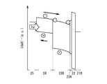
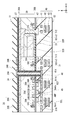
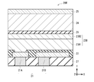
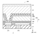
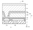
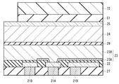
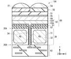
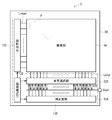
- the image pickup element 10 is, for example, a so-called vertical spectroscopic type in which one organic photoelectric conversion unit 20 and two inorganic photoelectric conversion units 32B and 32R are vertically laminated.
- the organic photoelectric conversion unit 20 is provided on the back surface (first surface 30A) side of the semiconductor substrate 30.
- the inorganic photoelectric conversion units 32B and 32R are embedded and formed in the semiconductor substrate 30, and are laminated in the thickness direction of the semiconductor substrate 30.
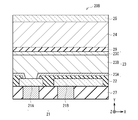
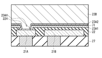
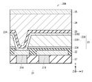
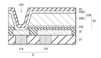
- the organic photoelectric conversion unit 20 further has an insulating layer 22 between the lower electrode 21 and the semiconductor layer 23.
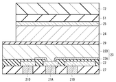
- the insulating layer 22 is provided over the entire surface of the pixel portion 1A, and has an opening 22H on the readout electrode 21A constituting the lower electrode 21, for example.
- the readout electrode 21A is electrically connected to the semiconductor layer 23 via the opening 22H.
- the first semiconductor layer 23A is formed from above the insulating layer 22 to the side surface of the opening 22H, and the readout electrode 21A and the second semiconductor layer 23B are directly connected to each other on the bottom surface of the opening 22H. There is.
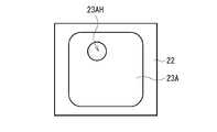
- the first semiconductor layer 23A has, for example, an opening 23AH in the opening 22H that exposes the read-out electrode 21A, and the second semiconductor layer 23B directly communicates with the read-out electrode 21A through these openings 22H and 23AH. It is connected.
- the opening 22H corresponds to a specific example of the "first opening” of the present disclosure
- the opening 23AH corresponds to a specific example of the "second opening" of the present disclosure.
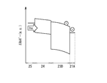
- FIG. 1 shows an example in which the semiconductor layer 23, the photoelectric conversion layer 24, and the upper electrode 25 are separately formed for each image sensor 10, the semiconductor layer 23, the photoelectric conversion layer 24, and the upper electrode 25 are shown.
- it may be provided as a continuous layer common to a plurality of image pickup devices 10.
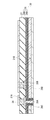
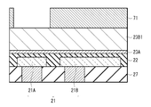
- an insulating layer 26 and an interlayer insulating layer 27 are laminated between the first surface 30A of the semiconductor substrate 30 and the lower electrode 21.
- a layer having a fixed charge (fixed charge layer) 26A and a dielectric layer 26B having an insulating property are laminated in this order from the semiconductor substrate 30 side.
- the organic photoelectric conversion unit 20 is an organic photoelectric conversion element that corresponds to a part or all of a selective wavelength range (for example, 450 nm or more and 650 nm or less), for example, absorbs green light and generates excitons. be.
- a selective wavelength range for example, 450 nm or more and 650 nm or less
- the semiconductor layer 23 is for accumulating the electric charge generated in the photoelectric conversion layer 24.
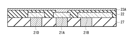
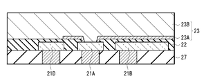
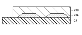
- the semiconductor layer 23 is provided between the lower electrode 21 and the photoelectric conversion layer 24, and the first semiconductor layer 23A and the second semiconductor layer 23B are laminated in this order from the lower electrode 21 side. It has a laminated structure.
- the first semiconductor layer 23A is provided on the insulating layer 22 that electrically separates the lower electrode 21 and the semiconductor layer 23, and covers the side surface of the opening 22H provided on the readout electrode 21A to open the opening. It has an opening 23AH in 22H that exposes the readout electrode 21A.
- the energy level (Ec) at the lowermost end of the conduction band of the first semiconductor layer 23A and the second semiconductor layer 23B can be controlled by, for example, the content of one or both of gallium (Ga) and zinc (Zn).
- the energy level (Ec1) at the lowermost end of the conduction band of the first semiconductor layer 23A is set to the second semiconductor layer.
- the thickness of the first semiconductor layer 23A is not particularly specified, but is preferably 1 nm or more and 50 nm or less, for example. This is because, in a thin film region having a thickness of less than 1 nm, electrons pass through the first semiconductor layer 23A due to the tunnel effect. This is because when the thickness is thicker than, for example, 50 nm, the capacitance increases and the saturated charge amount decreases.
- the thickness of the second semiconductor layer 23B is preferably 5 nm or more, for example. This is because, for example, in a thin film region having a thickness of less than 5 nm, there is an increased concern that electrons will flow back to the photoelectric conversion film during transfer.
- Examples of the organic material constituting the photoelectric conversion layer 24 include quinacridone derivatives, naphthalene derivatives, anthracene derivatives, phenanthrene derivatives, tetracene derivatives, pyrene derivatives, perylene derivatives and fluoranthene derivatives.
- the photoelectric conversion layer 24 is composed of a combination of two or more of the above organic materials.
- the organic material functions as a p-type semiconductor or an n-type semiconductor depending on the combination thereof.
- a cyanine-based dye or the like bonded by a squarylium group and a croconitecmethine group can be used.
- the metal complex dye include a dithiol metal complex dye, a metal phthalocyanine dye, a metal porphyrin dye, and a ruthenium complex dye. Of these, ruthenium complex dyes are particularly preferable, but are not limited to the above.
- the dielectric layer 26B is for preventing the reflection of light caused by the difference in refractive index between the semiconductor substrate 30 and the interlayer insulating layer 27.
- the constituent material of the dielectric layer 26B is preferably a material having a refractive index between the refractive index of the semiconductor substrate 30 and the refractive index of the interlayer insulating layer 27.
- Examples of the constituent material of the dielectric layer 26B include silicon oxide, TEOS, silicon nitride, silicon oxynitride (SiON) and the like.
- the reset transistor TR2rst is composed of a gate, a channel forming region, and a source / drain region.
- the gate of the reset transistor TR2rst is connected to the reset line RST2, and one source / drain region of the reset transistor TR2rst is connected to the power supply line VDD.
- the other source / drain region of the reset transistor TR2rst also serves as a floating diffusion FD2.
- the selection transistor TR2sel is composed of a gate, a channel forming region, and a source / drain region.
- the gate is connected to the selection line SEL2.
- One source / drain region constituting the selection transistor TR2sel shares an region with the other source / drain region constituting the amplifier transistor TR2amp.
- the other source / drain region constituting the selection transistor TR2sel is connected to the signal line (data output line) VSL2.
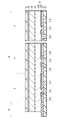
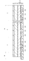
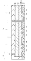
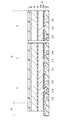
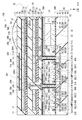
- FIG. 7 to 12 show the manufacturing method of the image sensor 10 in the order of processes.
- a p-well 31 is formed in the semiconductor substrate 30, and for example, n-type inorganic photoelectric conversion units 32B and 32R are formed in the p-well 31.
- a p + region is formed in the vicinity of the first surface 30A of the semiconductor substrate 30.
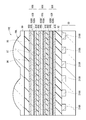
- the organic photoelectric conversion unit 20 is connected to the gate Gamp of the amplifier transistor TR1amp and the floating diffusion FD1 via the through electrode 34. Therefore, the electrons of the excitons generated by the organic photoelectric conversion unit 20 are taken out from the lower electrode 21 side, transferred to the second surface 30S2 side of the semiconductor substrate 30 via the through electrode 34, and accumulated in the floating diffusion FD1. NS.
- the amplifier transistor TR1amp modulates the amount of charge generated in the organic photoelectric conversion unit 20 into a voltage.
- the reset gate Grst of the reset transistor TR1rst is arranged next to the floating diffusion FD1. As a result, the electric charge accumulated in the floating diffusion FD1 is reset by the reset transistor TR1rst.
- the image sensor 10 is reset at a later stage of the storage period. Specifically, at timing t1, the scanning unit changes the voltage of the reset signal RST from a low level to a high level. As a result, in the unit pixel P, the reset transistor TR1rst is turned on, and as a result, the voltage of the floating diffusion FD1 is set to the power supply voltage, and the voltage of the floating diffusion FD1 is reset (reset period).
- the potential V1 is applied to the read electrode 21A from the drive circuit again, and the potential V2 is applied to the storage electrode 21B.
- the electric charge generated by the photoelectric conversion is attracted to the storage electrode 21B and accumulated in the region of the photoelectric conversion layer 24 facing the storage electrode 21B (accumulation period).
- the inorganic photoelectric conversion unit 32R electrons corresponding to the incident red light are accumulated in the n region of the inorganic photoelectric conversion unit 32R, and the accumulated electrons are transferred to the floating diffusion FD3 by the transfer transistor Tr3.
- the lower electrode 21 composed of the readout electrode 21A and the storage electrode 21B and the photoelectric conversion layer 24 each have an energy level (Ec) at the lowermost end of a predetermined conduction band.
- the semiconductor layer 23 composed of the first semiconductor layer 23A and the second semiconductor layer 23B is provided.
- the first semiconductor layer 23A and the second semiconductor layer 23B are laminated in this order from the lower electrode 21 side, and the first semiconductor layer 23A is from the energy level (Ec2) at the lowermost end of the conduction band of the second semiconductor layer 23B.
- Ec1 energy level at the bottom of the shallow conduction band.
- the protective layer 29 is for preventing the desorption of oxygen from the oxide semiconductor material constituting the semiconductor layer 23.
- the material constituting the protective layer 29 include TiO 2 , titanium silicate (TiSiO), niobium oxide (Nb 2 O 5 ), TaO x and the like.
- the thickness of the protective layer 29 is effective if it is, for example, a single atomic layer, and is preferably 0.5 nm or more and 10 nm or less, for example.
- the high-concentration carrier region 23X is formed in a region in contact with the readout electrode 21A, and has a higher carrier concentration than the other regions, preferably 1E17 or more. This lowers the barrier between the readout electrode 21A and the second semiconductor layer 23b.
- the openings 22H and 23AH of the insulating layer 22 and the first semiconductor layer 23A on the readout electrode 21A have the same side surfaces. have.
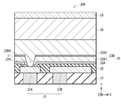
- FIG. 19 schematically shows a cross-sectional configuration of a main part (organic photoelectric conversion unit 20E) of the image pickup device of the modified example 5 of the present disclosure.
- a main part organic photoelectric conversion unit 20E
- FIG. 19 schematically shows a cross-sectional configuration of a main part (organic photoelectric conversion unit 20E) of the image pickup device of the modified example 5 of the present disclosure.
- the opening 23AH of the first semiconductor layer 23A is provided in the opening 22H of the insulating layer 22
- the present invention is not limited to this, and for example, as shown in FIG. 19, the outside of the opening 22H. It may be provided on the insulating layer 22 of the above.
- the process margin at the time of manufacturing is widened, and the manufacturing yield can be improved.
- a voltage can be applied independently to the read electrode 21A, the storage electrode 21B, and the transfer electrode 21C.
- the potential V5 is applied to the reading electrode 21A
- the potential V6 is applied to the storage electrode 21B
- the potential V7 (V5> V6> V7) is applied to the transfer electrode 21C during the transfer period after the completion of the reset operation.
- the electric charge accumulated above the storage electrode 21B moves from the storage electrode 21B to the transfer electrode 21C and the read-out electrode 21A in this order, and is read out to the floating diffusion FD1.
- FIG. 21 schematically shows a cross-sectional configuration of a main part (organic photoelectric conversion part 20G) of the image pickup device of the modification 7 of the present disclosure.
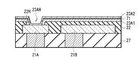
- the organic photoelectric conversion unit 20G of this modification is different from the above embodiment in that the first semiconductor layer 23A is a laminated film (first semiconductor layers 23A1, 23A2).
- the organic photoelectric conversion unit 20G of this modification is formed as follows, for example.
- the first semiconductor layer 23A2 is formed on the first semiconductor layer 23A1 on which the resist 71 remains, for example, by using a sputtering method to have a thickness of, for example, 1 nm to 10 nm.
- the second semiconductor layer 23B is formed by using, for example, a sputtering method.
- the photoelectric conversion layer 24 and the upper electrode 25 are formed on the second semiconductor layer 23B in the same manner as in the above embodiment.
- the organic photoelectric conversion unit 20G shown in FIG. 21 is completed.
- the resist 71 remaining in the layer of the first semiconductor layer 23A or the second semiconductor layer 23B can be confirmed by using, for example, secondary ion mass spectrometry (SIMS).
- the resist 71 is a resist for exposure of a KrF excimer laser such as a polyhydroxystyrene (PHS) resin containing, for example, a chemically amplified photoacid generator (PAG), ethyl lactate and methoxypropyl acetate (MPA). It contains a lot of carbon.
- PSG polyhydroxystyrene
- PAG chemically amplified photoacid generator
- MPA methoxypropyl acetate
- the resist 71 contains more carbon in the layer in which the resist 71 remains (for example, the first semiconductor layer 23A) than in other regions. Therefore, the resist 71 can be confirmed as a carbon peak by SIMS.
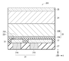
- FIG. 30 schematically shows a cross-sectional configuration of a main part (organic photoelectric conversion part 20M) of the image pickup device of the modification 9 of the present disclosure.
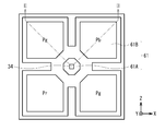
- FIG. 31 schematically shows the overall planar configuration of the image pickup apparatus 1 using the organic photoelectric conversion unit 20. Note that FIG. 30 shows a cross section taken along line II-II shown in FIG. 31.
- the second semiconductor layer 23B is laminated in this order from the lower electrode 11 side, in which a crystalline layer (crystal layer 23B1) and an amorphous layer (amorphous layer 23B2) are laminated. It is different from the above-described embodiment in that the laminated film is formed.
- FIG. 32A shows the energy levels of the insulating layer 22, the first semiconductor layer 23A, the second semiconductor layer 23B (crystal layer 23B1 and amorphous layer 23B2), the protective layer 29, and the photoelectric conversion layer 24 laminated on the storage electrode 21B. It represents.
- FIG. 32B shows the energies of the insulating layer 22, the second semiconductor layer 23B (crystal layer 23B1 and amorphous layer 23B2), the protective layer 29, and the photoelectric conversion layer 24 laminated in the openings 22H and 23AH provided on the readout electrode 21A. It represents the level.
- the surface of the oxide semiconductor layer may be damaged and deteriorated.
- a layer made of a material different from each material is inserted between the oxide semiconductor layer and the inorganic oxide film, the number of interfaces between different materials increases, and traps at the interfaces between different materials increase the oxide from the photoelectric conversion layer. Transfer of charge to the semiconductor layer may be hindered.
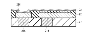
- batch processing is performed up to the second semiconductor layer 23B using, for example, dry etching.
- the resist 72 functions as a mask until the middle of the etching process, but the resist 72 disappears during the etching process, and then the protective layer 51 behaves as a hard mask.
- the resist 72 remains as a mask up to the photoelectric conversion layer 24 (FIG. 41E), but at the processing stage of the protective layer 29, for example, the resist 72 is etched together with the protective layer 29 and disappears (FIG. 41E). 41F).
- the protective layer 51 serves as a hard mask and the second semiconductor layer 23B is etched (FIG. 41G).
- both the semiconductor layer 23 and the protective layer 51 that serves as a hard mask during etching of the semiconductor layer 23 in this configuration are oxides, the protective layer 51 is also etched and damaged when the semiconductor layer 23 is etched. .. This series of steps has low controllability, and the photoelectric conversion layer 24 and the protective layer 51 may be damaged.
- the film thickness of the inorganic oxide film (protective layer 51) serving as a resist or a hard mask can be considered.
- thickening the protective layer 51 may cause side effects such as generation of film stress.
- the generation of film stress causes peeling of the underlying photoelectric conversion layer 24.
- the total design is changed.
- the dielectric constant of silicon oxide (for example, SiO 2 ) constituting the insulating layer 22 is about 4, and the dielectric constant of IGZO forming the first semiconductor layer 23A and the second semiconductor layer 23B is about 16.
- the film thicknesses of SiO 2 and IGZO are 10 nm each and the capacity of SiO 2 is C
- the capacity of IGZO is 4C.
- the organic photoelectric conversion unit 60 is composed of, for example, a lower electrode 61, an insulating layer 62, a semiconductor layer 63, a photoelectric conversion layer 64 and an upper electrode 65, and includes a lower electrode 61, an insulating layer 62, a semiconductor layer 63, a photoelectric conversion layer 64 and an upper portion.
- Each of the electrodes 65 has the same configuration as the organic photoelectric conversion unit 20 in the above embodiment.
- the inorganic photoelectric conversion unit 32 detects light in a wavelength range different from that of the organic photoelectric conversion unit 60.
- the light in the visible light region (red light (R), green light (G), and blue light (B)) is provided with each color filter.
- the organic photoelectric conversion units 20 and 80 and the inorganic photoelectric conversion unit 32 selectively detect light in different wavelength ranges and perform photoelectric conversion.
- the organic photoelectric conversion unit 20 acquires a green (G) color signal.
- the organic photoelectric conversion unit 80 acquires a blue (B) color signal.
- the inorganic photoelectric conversion unit 32 acquires a red (R) color signal.
- the image sensor 10C can acquire a plurality of types of color signals in one pixel without using a color filter.
- the readout electrode 71A is electrically connected to the first semiconductor layer 72A via an opening 72H provided in the insulating layer 72.
- the semiconductor layer 73, the photoelectric conversion layer 74, and the upper electrode 75 are separately formed for each image sensor 10D.
- the semiconductor layer 73, the photoelectric conversion layer 74, and the upper electrode 75 are provided as a continuous layer common to a plurality of image pickup devices 10D. You may.
- the through electrode 34X is electrically connected to the readout electrode 21A of the organic photoelectric conversion unit 20 as in the through electrode 34 in the above embodiment, and the organic photoelectric conversion unit 20 is connected to the amplifier via the through electrode 34X. It is connected to the gate Gamp of the transistor AMP and the source / drain region 36B1 of one of the reset transistors RST (reset transistor Tr1rst) that also serves as the floating diffusion FD1.
- the upper end of the through electrode 34X is connected to the readout electrode 21A via, for example, the pad portion 39A and the upper first contact 39C.
- a protective layer 98 and an on-chip lens layer 99 having an on-chip lens 99L on the surface are provided on the blue photoelectric conversion unit 90B.
- a red power storage layer 310R, a green power storage layer 310G, and a blue power storage layer 310B are provided in the semiconductor substrate 30.
- the light incident on the on-chip lens 99L is photoelectrically converted by the red photoelectric conversion unit 90R, the green photoelectric conversion unit 90G, and the blue photoelectric conversion unit 90B, from the red photoelectric conversion unit 90R to the red storage layer 310R, and from the green photoelectric conversion unit 90G.
- Signal charges are sent to the green storage layer 310G from the blue photoelectric conversion unit 90B to the blue storage layer 310B, respectively.
- the signal charge may be either an electron or a hole generated by photoelectric conversion, but the case where the electron is read out as a signal charge will be described below as an example.
- the semiconductor substrate 30 is composed of, for example, a p-type silicon substrate.
- the red storage layer 310R, the green storage layer 310G, and the blue storage layer 310B provided on the semiconductor substrate 30 each include an n-type semiconductor region, and the red photoelectric conversion unit 90R and the green photoelectric conversion unit are included in the n-type semiconductor region.
- the signal charges (electrons) supplied from the 90G and the blue photoelectric conversion unit 90B are accumulated.
- the n-type semiconductor region of the red storage layer 310R, the green storage layer 310G, and the blue storage layer 310B is formed, for example, by doping the semiconductor substrate 30 with n-type impurities such as phosphorus (P) or arsenic (As). ..
- the semiconductor substrate 30 may be provided on a support substrate (not shown) made of glass or the like.
- the insulating layer 92 is, for example, a single-layer film composed of one of silicon oxide (SiO x ), silicon nitride (SiN x ), silicon oxynitride (SiON), hafnium oxide (HfO x ), and the like, or among these. It is composed of a laminated film composed of two or more of the above. Further, the insulating layer 92 may be formed by using an organic insulating material. Although not shown, the insulating layer 92 is for connecting the red storage layer 310R and the red photoelectric conversion unit 90R, the green storage layer 310G and the green photoelectric conversion unit 90G, and the blue storage layer 310B and the blue photoelectric conversion unit 90B, respectively. Plugs and electrodes are provided.
- the lower electrodes 91R, 91G, 91B are made of, for example, a conductive material having light transmission, for example, ITO.
- a tin oxide (SnO 2 ) -based material to which a dopant is added or a zinc oxide-based material obtained by adding a dopant to zinc oxide (ZnO) may be used.
- the zinc oxide-based material include aluminum zinc oxide (AZO) to which aluminum (Al) is added as a dopant, gallium zinc oxide (GZO) to which gallium (Ga) is added, and indium zinc to which indium (In) is added.
- Oxide (IZO) can be mentioned.
- the addition to, IGZO, ITZO, CuI, InSbO 4, ZnMgO, CuInO 2, MgIN 2 O 4, CdO may be used ZnSnO 3, and the like.
- the organic photoelectric conversion unit 90R the first semiconductor layer 93RA, the second semiconductor layer 93RB, the photoelectric conversion layer 94R, and the upper electrode 95R are laminated in this order from the lower electrode 91R side.
- the first semiconductor layers 93RA, 93GA, 93BA and the second semiconductor layers 93RB, 93GB, 93BB have the same configurations as the first semiconductor layer 23A and the second semiconductor layer 23B, respectively.
- the photoelectric conversion layers 94R, 94G, and 94B convert light energy into electrical energy, and each absorbs light in a selective wavelength range, performs photoelectric conversion, and transmits light in another wavelength range.
- the light in the selective wavelength range is, for example, light in a wavelength range of 620 nm or more and less than 750 nm in the photoelectric conversion layer 94R.
- the photoelectric conversion layer 94G for example, the light has a wavelength range of 495 nm or more and less than 620 nm.
- the photoelectric conversion layer 94B is, for example, light having a wavelength range of 400 nm or more and less than 495 nm.
- the upper electrodes 95R, 95G, 95B are made of a conductive material having light transmission, for example, ITO.
- the upper electrodes 95R, 95G, and 95B may be made of a conductive material such as gold (Au), silver (Ag), copper (Cu), and aluminum (Al).
- the image pickup device 10E of the present modification has a configuration in which three organic photoelectric conversion units (red photoelectric conversion unit 90R, green photoelectric conversion unit 90G, and blue photoelectric conversion unit 90B) are laminated, and each organic photoelectric conversion unit is used.
- the parts 90R, 90G, 90B similarly to the organic photoelectric conversion part 20 in the above embodiment, between the lower electrodes 91R, 91G, 91B and the photoelectric conversion layers 94R, 94G, 94B, Ec1> Ec2, respectively.
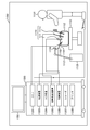
- FIG. 53 shows the overall configuration of an image pickup device (imaging device 1) using the image pickup device (for example, the image pickup device 10) of the present disclosure for each pixel.
- the image pickup apparatus 1 is a CMOS image sensor, and has a pixel portion 1A as an imaging area on a semiconductor substrate 30, and in a peripheral region of the pixel portion 1A, for example, a row scanning unit 131, a horizontal selection unit 133, and the like. It has a peripheral circuit unit 130 including a row scanning unit 134 and a system control unit 132.
- the row scanning unit 131 is a pixel driving unit that is composed of a shift register, an address decoder, and the like, and drives each unit pixel P of the pixel unit 1A, for example, in row units.
- the signal output from each unit pixel P of the pixel row selected and scanned by the row scanning unit 131 is supplied to the horizontal selection unit 133 through each of the vertical signal lines Lsig.
- the horizontal selection unit 133 is composed of an amplifier, a horizontal selection switch, and the like provided for each vertical signal line Lsig.
- the circuit portion including the row scanning unit 131, the horizontal selection unit 133, the column scanning unit 134, and the horizontal signal line 135 may be formed directly on the semiconductor substrate 30, or may be arranged on the external control IC. It may be. Further, those circuit portions may be formed on another substrate connected by a cable or the like.
- the system control unit 132 receives a clock given from the outside of the semiconductor substrate 30, data for instructing an operation mode, and the like, and outputs data such as internal information of the image pickup apparatus 1.
- the system control unit 132 further has a timing generator that generates various timing signals, and the row scanning unit 131, the horizontal selection unit 133, the column scanning unit 134, and the like based on the various timing signals generated by the timing generator. Controls the drive of peripheral circuits.
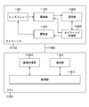
- the optical system 210 guides the image light (incident light) from the subject to the pixel portion 1A of the image pickup apparatus 1.
- the optical system 210 may be composed of a plurality of optical lenses.
- the shutter device 211 controls the light irradiation period and the light blocking period for the image pickup device 1.
- the drive unit 213 controls the transfer operation of the image pickup device 1 and the shutter operation of the shutter device 211.
- the signal processing unit 212 performs various signal processing on the signal output from the image pickup apparatus 1.
- the video signal Dout after signal processing is stored in a storage medium such as a memory, or is output to a monitor or the like.
- the technology according to the present disclosure can be applied to various products.
- the techniques according to the present disclosure may be applied to endoscopic surgery systems.
- the internal information acquisition system 10001 is composed of a capsule endoscope 10100 and an external control device 10200.
- the capsule endoscope 10100 is swallowed by the patient at the time of examination.
- the capsule endoscope 10100 has an imaging function and a wireless communication function, and moves inside an organ such as the stomach or intestine by peristaltic movement or the like until it is naturally excreted from the patient, and inside the organ.
- Images (hereinafter, also referred to as internal organ images) are sequentially imaged at predetermined intervals, and information about the internal organ images is sequentially wirelessly transmitted to an external control device 10200 outside the body.
- the external control device 10200 comprehensively controls the operation of the internal information acquisition system 10001. Further, the external control device 10200 receives information about the internal image transmitted from the capsule endoscope 10100, and based on the information about the received internal image, the internal image is displayed on a display device (not shown). Generate image data to display.
- the internal information acquisition system 10001 in this way, it is possible to obtain an internal image of the inside of the patient at any time from the time when the capsule endoscope 10100 is swallowed until it is discharged.
- the image processing unit 10113 is composed of processors such as a CPU (Central Processing Unit) and a GPU (Graphics Processing Unit), and performs various signal processing on the image signal generated by the imaging unit 10112.
- the image processing unit 10113 provides the signal-processed image signal to the wireless communication unit 10114 as RAW data.
- the wireless communication unit 10114 performs predetermined processing such as modulation processing on the image signal that has been signal-processed by the image processing unit 10113, and transmits the image signal to the external control device 10200 via the antenna 10114A. Further, the wireless communication unit 10114 receives a control signal related to drive control of the capsule endoscope 10100 from the external control device 10200 via the antenna 10114A. The wireless communication unit 10114 provides the control unit 10117 with a control signal received from the external control device 10200.
- the power supply unit 10116 is composed of a secondary battery and stores the electric power generated by the power supply unit 10115.
- FIG. 55 in order to avoid complication of the drawing, the illustration of the arrow or the like indicating the power supply destination from the power supply unit 10116 is omitted, but the power stored in the power supply unit 10116 is the light source unit 10111. , Is supplied to the imaging unit 10112, the image processing unit 10113, the wireless communication unit 10114, and the control unit 10117, and can be used to drive these.
- the above is an example of an in-vivo information acquisition system to which the technology according to the present disclosure can be applied.
- the technique according to the present disclosure can be applied to, for example, the imaging unit 10112 among the configurations described above. This improves the detection accuracy.
- An optical system and an image pickup element are provided inside the camera head 11102, and the reflected light (observation light) from the observation target is focused on the image pickup element by the optical system.
- the observation light is photoelectrically converted by the image sensor, and an electric signal corresponding to the observation light, that is, an image signal corresponding to the observation image is generated.
- the image signal is transmitted as RAW data to the camera control unit (CCU: Camera Control Unit) 11201.
- CCU Camera Control Unit
- the display device 11202 displays an image based on the image signal processed by the CCU 11201 under the control of the CCU 11201.
- the light source device 11203 is composed of, for example, a light source such as an LED (light emission diode), and supplies irradiation light to the endoscope 11100 when photographing an operating part or the like.
- a light source such as an LED (light emission diode)
- the drive unit 11403 is composed of an actuator, and the zoom lens and focus lens of the lens unit 11401 are moved by a predetermined distance along the optical axis under the control of the camera head control unit 11405. As a result, the magnification and focus of the image captured by the imaging unit 11402 can be adjusted as appropriate.
- the image processing unit 11412 performs various image processing on the image signal which is the RAW data transmitted from the camera head 11102.
- the communication is performed by wire using the transmission cable 11400, but the communication between the camera head 11102 and the CCU11201 may be performed wirelessly.
- the above is an example of an endoscopic surgery system to which the technology according to the present disclosure can be applied.
- the technique according to the present disclosure can be applied to the imaging unit 11402 among the configurations described above. By applying the technique according to the present disclosure to the imaging unit 11402, the detection accuracy is improved.
- the technique according to the present disclosure may be applied to other, for example, a microscopic surgery system.
- the technology according to the present disclosure can be applied to various products.
- the technology according to the present disclosure includes any type of movement such as automobiles, electric vehicles, hybrid electric vehicles, motorcycles, bicycles, personal mobility, airplanes, drones, ships, robots, construction machines, agricultural machines (tractors), and the like. It may be realized as a device mounted on the body.
- FIG. 58 is a block diagram showing a schematic configuration example of a vehicle control system, which is an example of a mobile control system to which the technique according to the present disclosure can be applied.
- the vehicle control system 12000 includes a plurality of electronic control units connected via the communication network 12001.
- the vehicle control system 12000 includes a drive system control unit 12010, a body system control unit 12020, an outside information detection unit 12030, an in-vehicle information detection unit 12040, and an integrated control unit 12050.
- a microcomputer 12051, an audio image output unit 12052, and an in-vehicle network I / F (interface) 12053 are shown as a functional configuration of the integrated control unit 12050.
- the imaging unit 12031 is an optical sensor that receives light and outputs an electric signal according to the amount of the light received.
- the image pickup unit 12031 can output an electric signal as an image or can output it as distance measurement information. Further, the light received by the imaging unit 12031 may be visible light or invisible light such as infrared light.
- the in-vehicle information detection unit 12040 detects the in-vehicle information.
- a driver state detection unit 12041 that detects the driver's state is connected to the in-vehicle information detection unit 12040.
- the driver state detection unit 12041 includes, for example, a camera that images the driver, and the in-vehicle information detection unit 12040 determines the degree of fatigue or concentration of the driver based on the detection information input from the driver state detection unit 12041. It may be calculated, or it may be determined whether the driver is dozing.
- the microcomputer 12051 can output a control command to the body system control unit 12020 based on the information outside the vehicle acquired by the vehicle exterior information detection unit 12030.
- the microcomputer 12051 controls the headlamps according to the position of the preceding vehicle or the oncoming vehicle detected by the external information detection unit 12030, and performs coordinated control for the purpose of anti-glare such as switching the high beam to the low beam. It can be carried out.
- the audio image output unit 12052 transmits the output signal of at least one of the audio and the image to the output device capable of visually or audibly notifying the passenger or the outside of the vehicle of the information.
- an audio speaker 12061, a display unit 12062, and an instrument panel 12063 are exemplified as output devices.
- the display unit 12062 may include, for example, at least one of an onboard display and a heads-up display.
- FIG. 59 is a diagram showing an example of the installation position of the imaging unit 12031.
- the imaging units 12101, 12102, 12103, 12104, 12105 are provided at positions such as the front nose, side mirrors, rear bumpers, back doors, and the upper part of the windshield in the vehicle interior of the vehicle 12100, for example.
- the image pickup unit 12101 provided on the front nose and the image pickup section 12105 provided on the upper part of the windshield in the vehicle interior mainly acquire an image in front of the vehicle 12100.
- the imaging units 12102 and 12103 provided in the side mirrors mainly acquire images of the side of the vehicle 12100.
- the imaging unit 12104 provided on the rear bumper or the back door mainly acquires an image of the rear of the vehicle 12100.
- the imaging unit 12105 provided on the upper part of the windshield in the vehicle interior is mainly used for detecting a preceding vehicle, a pedestrian, an obstacle, a traffic light, a traffic sign, a lane, or the like.
- At least one of the imaging units 12101 to 12104 may have a function of acquiring distance information.
- at least one of the image pickup units 12101 to 12104 may be a stereo camera composed of a plurality of image pickup elements, or an image pickup element having pixels for phase difference detection.
- the microcomputer 12051 has a distance to each three-dimensional object within the imaging range 12111 to 12114 based on the distance information obtained from the imaging units 12101 to 12104, and a temporal change of this distance (relative velocity with respect to the vehicle 12100). By obtaining can. Further, the microcomputer 12051 can set an inter-vehicle distance to be secured in front of the preceding vehicle in advance, and can perform automatic braking control (including follow-up stop control), automatic acceleration control (including follow-up start control), and the like. In this way, it is possible to perform coordinated control for the purpose of automatic driving or the like in which the vehicle travels autonomously without depending on the operation of the driver.
- automatic braking control including follow-up stop control
- automatic acceleration control including follow-up start control
- the microcomputer 12051 converts three-dimensional object data related to a three-dimensional object into two-wheeled vehicles, ordinary vehicles, large vehicles, pedestrians, electric poles, and other three-dimensional objects based on the distance information obtained from the imaging units 12101 to 12104. It can be classified and extracted and used for automatic avoidance of obstacles. For example, the microcomputer 12051 distinguishes obstacles around the vehicle 12100 into obstacles that can be seen by the driver of the vehicle 12100 and obstacles that are difficult to see. Then, the microcomputer 12051 determines the collision risk indicating the risk of collision with each obstacle, and when the collision risk is equal to or higher than the set value and there is a possibility of collision, the microcomputer 12051 is used via the audio speaker 12061 or the display unit 12062. By outputting an alarm to the driver and performing forced deceleration and avoidance steering via the drive system control unit 12010, driving support for collision avoidance can be provided.
- At least one of the imaging units 12101 to 12104 may be an infrared camera that detects infrared rays.
- the microcomputer 12051 can recognize a pedestrian by determining whether or not a pedestrian is present in the captured image of the imaging units 12101 to 12104.
- pedestrian recognition includes, for example, a procedure for extracting feature points in an image captured by an imaging unit 12101 to 12104 as an infrared camera, and a pattern matching process for a series of feature points indicating the outline of an object to determine whether or not the pedestrian is a pedestrian. It is done by the procedure to determine.
- the audio image output unit 12052 When the microcomputer 12051 determines that a pedestrian is present in the captured images of the imaging units 12101 to 12104 and recognizes the pedestrian, the audio image output unit 12052 outputs a square contour line for emphasizing the recognized pedestrian.
- the display unit 12062 is controlled so as to superimpose and display. Further, the audio image output unit 12052 may control the display unit 12062 so as to display an icon or the like indicating a pedestrian at a desired position.
- the organic photoelectric conversion unit 20 that detects green light and the inorganic photoelectric conversion units 32B and 32R that detect blue light and red light are laminated as an image sensor.
- the contents of the present disclosure are not limited to such a structure.
- the organic photoelectric conversion unit may detect red light or blue light, or the inorganic photoelectric conversion unit may detect green light.
- a plurality of electrodes constituting the lower electrode 21 two electrodes, a readout electrode 21A and a storage electrode 21B, or a readout electrode 21A, a storage electrode 21B, a transfer electrode 21C, a readout electrode 21A, and a storage electrode 21A are stored.
- a discharge electrode four or more electrodes such as a discharge electrode may be provided in addition to this.
- the image pickup device described. (15) The image pickup device according to any one of (1) to (14), wherein both the first layer and the second layer have amorphous properties. (16) The image pickup device according to any one of (1) to (14), wherein one of the first layer and the second layer has a crystalline property and the other has an amorphous property. .. (17) The second layer is any one of the above (2) to (16), which has a layer in the second layer containing more carbon than other regions in the second layer. The image sensor according to. (18) The image pickup according to (17) above, wherein the second layer covers the side surface and the bottom surface of the first opening, and the carbon-rich layer is provided outside the first opening in the layer. element.
- the image pickup device according to one.
- the image pickup device according to any one of (1) to (26), wherein the second layer has a thickness of 1 nm or more and 50 nm or less.
- the image pickup device according to any one of (1) to (27), further comprising a fourth electrode between the first electrode and the second electrode.
- the image pickup device according to (28), wherein the fourth electrode is provided below the first electrode and the second electrode.
- the first layer has a laminated structure of a layer having crystallinity and a layer having amorphousness.
- the image pickup device according to (36) or (37), wherein the end portion of the second layer and the second opening have a round shape in a plan view.
- the invention according to any one of (1) to (38), further comprising a fifth electrode to which a fixed potential is applied around the first electrode and the second electrode in a plan view.
- Image sensor (40) The image pickup device according to (39), wherein the first layer is formed above the fifth electrode without interposing the second layer. (41) The first electrode and the second electrode are arranged on the side opposite to the light incident surface with respect to the photoelectric conversion layer, according to any one of (1) to (40). Image sensor. (42) The image pickup device according to any one of (1) to (41), wherein a voltage is individually applied to the first electrode and the second electrode.
- the image sensor is The first electrode and the second electrode arranged in parallel, The first electrode and the third electrode arranged to face the second electrode, A photoelectric conversion layer provided between the first electrode and the second electrode and the third electrode, and At the lowermost end of the conduction band, which is provided between the first electrode and the second electrode and the photoelectric conversion layer and is shallower than the energy level at the lowermost end of the conduction band of the first layer and the first layer.
- An image pickup apparatus having a second layer having an energy level and a semiconductor layer laminated in order from the photoelectric conversion layer side.
Landscapes
- Physics & Mathematics (AREA)
- Electromagnetism (AREA)
- Solid State Image Pick-Up Elements (AREA)
- Light Receiving Elements (AREA)
- Life Sciences & Earth Sciences (AREA)
- Engineering & Computer Science (AREA)
- Sustainable Development (AREA)
- Sustainable Energy (AREA)
Priority Applications (5)
| Application Number | Priority Date | Filing Date | Title |
|---|---|---|---|
| CN202180023417.8A CN115428157A (zh) | 2020-03-31 | 2021-03-24 | 摄像元件和摄像装置 |
| KR1020227032091A KR102920107B1 (ko) | 2020-03-31 | 2021-03-24 | 촬상 소자 및 촬상 장치 |
| US17/915,619 US12464829B2 (en) | 2020-03-31 | 2021-03-24 | Imaging element and imaging device |
| EP21778942.9A EP4131386A4 (en) | 2020-03-31 | 2021-03-24 | Imaging element and imaging device |
| JP2022512044A JP7753193B2 (ja) | 2020-03-31 | 2021-03-24 | 撮像素子および撮像装置 |
Applications Claiming Priority (4)
| Application Number | Priority Date | Filing Date | Title |
|---|---|---|---|
| JP2020-064017 | 2020-03-31 | ||
| JP2020064017 | 2020-03-31 | ||
| JP2021045945 | 2021-03-19 | ||
| JP2021-045945 | 2021-03-19 |
Publications (1)
| Publication Number | Publication Date |
|---|---|
| WO2021200509A1 true WO2021200509A1 (ja) | 2021-10-07 |
Family
ID=77927124
Family Applications (1)
| Application Number | Title | Priority Date | Filing Date |
|---|---|---|---|
| PCT/JP2021/012401 Ceased WO2021200509A1 (ja) | 2020-03-31 | 2021-03-24 | 撮像素子および撮像装置 |
Country Status (7)
| Country | Link |
|---|---|
| US (1) | US12464829B2 (https=) |
| EP (1) | EP4131386A4 (https=) |
| JP (1) | JP7753193B2 (https=) |
| KR (1) | KR102920107B1 (https=) |
| CN (1) | CN115428157A (https=) |
| TW (1) | TWI889786B (https=) |
| WO (1) | WO2021200509A1 (https=) |
Cited By (2)
| Publication number | Priority date | Publication date | Assignee | Title |
|---|---|---|---|---|
| WO2023153308A1 (ja) * | 2022-02-14 | 2023-08-17 | ソニーセミコンダクタソリューションズ株式会社 | 光電変換素子および光検出装置 |
| WO2024070293A1 (ja) * | 2022-09-30 | 2024-04-04 | ソニーセミコンダクタソリューションズ株式会社 | 光電変換素子および光検出装置 |
Families Citing this family (2)
| Publication number | Priority date | Publication date | Assignee | Title |
|---|---|---|---|---|
| CN113302761B (zh) * | 2019-02-15 | 2025-12-19 | 索尼半导体解决方案公司 | 摄像元件和摄像装置 |
| WO2025083961A1 (ja) * | 2023-10-20 | 2025-04-24 | ソニーセミコンダクタソリューションズ株式会社 | 光検出装置 |
Citations (7)
| Publication number | Priority date | Publication date | Assignee | Title |
|---|---|---|---|---|
| JP2010003901A (ja) * | 2008-06-20 | 2010-01-07 | Fujifilm Corp | 光電変換素子及び固体撮像素子 |
| JP2013020998A (ja) * | 2011-07-07 | 2013-01-31 | Renesas Electronics Corp | 半導体装置およびその製造方法 |
| JP2014165399A (ja) * | 2013-02-26 | 2014-09-08 | Toshiba Corp | 固体撮像装置 |
| WO2019035252A1 (ja) | 2017-08-16 | 2019-02-21 | ソニー株式会社 | 撮像素子、積層型撮像素子及び固体撮像装置 |
| JP2019047294A (ja) * | 2017-08-31 | 2019-03-22 | ソニーセミコンダクタソリューションズ株式会社 | 固体撮像装置および固体撮像装置の制御方法 |
| JP2020064017A (ja) | 2018-10-19 | 2020-04-23 | 株式会社日立製作所 | 温度検知材料、それを用いた温度検知インク、温度インジケータ、及び物品管理システム |
| JP2021045945A (ja) | 2019-09-20 | 2021-03-25 | ファナック株式会社 | 射出成形機の制御装置および制御方法 |
Family Cites Families (14)
| Publication number | Priority date | Publication date | Assignee | Title |
|---|---|---|---|---|
| JP5460118B2 (ja) * | 2008-05-14 | 2014-04-02 | 富士フイルム株式会社 | 光電変換素子、及び撮像素子 |
| JP2014127545A (ja) * | 2012-12-26 | 2014-07-07 | Sony Corp | 固体撮像素子およびこれを備えた固体撮像装置 |
| JP2015043370A (ja) * | 2013-08-26 | 2015-03-05 | シャープ株式会社 | 光電変換装置 |
| EP3376543A4 (en) * | 2015-11-12 | 2018-11-21 | Panasonic Intellectual Property Management Co., Ltd. | Photosensor |
| JP6780421B2 (ja) * | 2016-03-01 | 2020-11-04 | ソニー株式会社 | 撮像素子、積層型撮像素子及び固体撮像装置、並びに、固体撮像装置の駆動方法 |
| WO2017208806A1 (ja) * | 2016-06-02 | 2017-12-07 | ソニー株式会社 | 撮像素子および撮像素子の製造方法ならびに撮像装置 |
| WO2018025540A1 (ja) * | 2016-08-03 | 2018-02-08 | ソニー株式会社 | 撮像素子、積層型撮像素子及び固体撮像装置 |
| JP2019036641A (ja) * | 2017-08-16 | 2019-03-07 | ソニー株式会社 | 撮像素子、積層型撮像素子及び固体撮像装置 |
| KR102491856B1 (ko) * | 2017-12-18 | 2023-01-27 | 삼성전자주식회사 | 복수의 양자점층을 포함하는 광전 소자 |
| WO2019151049A1 (ja) | 2018-01-31 | 2019-08-08 | ソニー株式会社 | 光電変換素子、固体撮像装置及び電子装置 |
| WO2019150987A1 (ja) | 2018-01-31 | 2019-08-08 | ソニー株式会社 | 光電変換素子および撮像装置 |
| WO2019181456A1 (ja) * | 2018-03-19 | 2019-09-26 | ソニーセミコンダクタソリューションズ株式会社 | 固体撮像素子および固体撮像装置 |
| CN112385044B (zh) * | 2018-07-17 | 2024-09-17 | 索尼半导体解决方案公司 | 摄像元件、层叠型摄像元件和固态摄像装置 |
| EP3832725A4 (en) * | 2018-07-31 | 2021-08-25 | Sony Semiconductor Solutions Corporation | IMAGING ELEMENT AND IMAGING DEVICE |
-
2021
- 2021-03-24 WO PCT/JP2021/012401 patent/WO2021200509A1/ja not_active Ceased
- 2021-03-24 KR KR1020227032091A patent/KR102920107B1/ko active Active
- 2021-03-24 EP EP21778942.9A patent/EP4131386A4/en active Pending
- 2021-03-24 US US17/915,619 patent/US12464829B2/en active Active
- 2021-03-24 CN CN202180023417.8A patent/CN115428157A/zh active Pending
- 2021-03-24 JP JP2022512044A patent/JP7753193B2/ja active Active
- 2021-03-30 TW TW110111645A patent/TWI889786B/zh active
Patent Citations (7)
| Publication number | Priority date | Publication date | Assignee | Title |
|---|---|---|---|---|
| JP2010003901A (ja) * | 2008-06-20 | 2010-01-07 | Fujifilm Corp | 光電変換素子及び固体撮像素子 |
| JP2013020998A (ja) * | 2011-07-07 | 2013-01-31 | Renesas Electronics Corp | 半導体装置およびその製造方法 |
| JP2014165399A (ja) * | 2013-02-26 | 2014-09-08 | Toshiba Corp | 固体撮像装置 |
| WO2019035252A1 (ja) | 2017-08-16 | 2019-02-21 | ソニー株式会社 | 撮像素子、積層型撮像素子及び固体撮像装置 |
| JP2019047294A (ja) * | 2017-08-31 | 2019-03-22 | ソニーセミコンダクタソリューションズ株式会社 | 固体撮像装置および固体撮像装置の制御方法 |
| JP2020064017A (ja) | 2018-10-19 | 2020-04-23 | 株式会社日立製作所 | 温度検知材料、それを用いた温度検知インク、温度インジケータ、及び物品管理システム |
| JP2021045945A (ja) | 2019-09-20 | 2021-03-25 | ファナック株式会社 | 射出成形機の制御装置および制御方法 |
Non-Patent Citations (1)
| Title |
|---|
| See also references of EP4131386A4 |
Cited By (2)
| Publication number | Priority date | Publication date | Assignee | Title |
|---|---|---|---|---|
| WO2023153308A1 (ja) * | 2022-02-14 | 2023-08-17 | ソニーセミコンダクタソリューションズ株式会社 | 光電変換素子および光検出装置 |
| WO2024070293A1 (ja) * | 2022-09-30 | 2024-04-04 | ソニーセミコンダクタソリューションズ株式会社 | 光電変換素子および光検出装置 |
Also Published As
| Publication number | Publication date |
|---|---|
| TW202143469A (zh) | 2021-11-16 |
| EP4131386A1 (en) | 2023-02-08 |
| KR20220160567A (ko) | 2022-12-06 |
| KR102920107B1 (ko) | 2026-01-30 |
| CN115428157A (zh) | 2022-12-02 |
| US20230215880A1 (en) | 2023-07-06 |
| JP7753193B2 (ja) | 2025-10-14 |
| TWI889786B (zh) | 2025-07-11 |
| EP4131386A4 (en) | 2023-09-27 |
| US12464829B2 (en) | 2025-11-04 |
| JPWO2021200509A1 (https=) | 2021-10-07 |
Similar Documents
| Publication | Publication Date | Title |
|---|---|---|
| US11792541B2 (en) | Solid-state imaging device and method of controlling solid-state imaging device | |
| CN113302761B (zh) | 摄像元件和摄像装置 | |
| WO2020026851A1 (ja) | 撮像素子および撮像装置 | |
| KR102920107B1 (ko) | 촬상 소자 및 촬상 장치 | |
| US20210104564A1 (en) | Photoelectric converter and solid-state imaging device | |
| KR102776688B1 (ko) | 촬상 소자 및 촬상 장치 | |
| WO2020017305A1 (ja) | 撮像素子および撮像装置 | |
| JPWO2019220897A1 (ja) | 撮像素子および電子機器並びに撮像素子の駆動方法 | |
| WO2022024799A1 (ja) | 光電変換素子および撮像装置 | |
| US20250194332A1 (en) | Photoelectric conversion element and photodetector | |
| JP7657160B2 (ja) | 撮像素子および撮像素子の製造方法 | |
| WO2021153294A1 (ja) | 撮像素子および撮像装置 | |
| US20250221142A1 (en) | Imaging element and method of manufacturing imaging element, and light detection device | |
| WO2024070293A1 (ja) | 光電変換素子および光検出装置 | |
| US12550466B2 (en) | Solid-state imaging element and electronic device | |
| WO2025100109A1 (ja) | 光検出素子および光検出装置 | |
| WO2024106235A1 (ja) | 光検出装置および光検出装置の製造方法ならびに電子機器 | |
| CN113678273A (zh) | 光电转换元件和摄像装置 |
Legal Events
| Date | Code | Title | Description |
|---|---|---|---|
| 121 | Ep: the epo has been informed by wipo that ep was designated in this application |
Ref document number: 21778942 Country of ref document: EP Kind code of ref document: A1 |
|
| ENP | Entry into the national phase |
Ref document number: 2022512044 Country of ref document: JP Kind code of ref document: A |
|
| NENP | Non-entry into the national phase |
Ref country code: DE |
|
| ENP | Entry into the national phase |
Ref document number: 2021778942 Country of ref document: EP Effective date: 20221031 |
|
| WWG | Wipo information: grant in national office |
Ref document number: 17915619 Country of ref document: US |