WO2021200406A1 - Dispositif à semi-conducteur - Google Patents
Dispositif à semi-conducteur Download PDFInfo
- Publication number
- WO2021200406A1 WO2021200406A1 PCT/JP2021/012062 JP2021012062W WO2021200406A1 WO 2021200406 A1 WO2021200406 A1 WO 2021200406A1 JP 2021012062 W JP2021012062 W JP 2021012062W WO 2021200406 A1 WO2021200406 A1 WO 2021200406A1
- Authority
- WO
- WIPO (PCT)
- Prior art keywords
- semiconductor device
- glass substrate
- hole
- frame
- insulating film
- Prior art date
Links
- 239000004065 semiconductor Substances 0.000 title claims abstract description 279
- 239000011521 glass Substances 0.000 claims abstract description 367
- 239000000758 substrate Substances 0.000 claims abstract description 356
- 229910052751 metal Inorganic materials 0.000 claims description 124
- 239000002184 metal Substances 0.000 claims description 124
- 239000000463 material Substances 0.000 claims description 63
- 239000006059 cover glass Substances 0.000 claims description 56
- 230000003287 optical effect Effects 0.000 claims description 20
- 230000000149 penetrating effect Effects 0.000 claims description 13
- 239000000945 filler Substances 0.000 claims description 7
- 238000004891 communication Methods 0.000 claims description 4
- 230000005484 gravity Effects 0.000 claims description 4
- 239000010408 film Substances 0.000 description 282
- 238000012986 modification Methods 0.000 description 44
- 230000004048 modification Effects 0.000 description 44
- 238000000034 method Methods 0.000 description 31
- 238000004519 manufacturing process Methods 0.000 description 28
- 229920005989 resin Polymers 0.000 description 24
- 239000011347 resin Substances 0.000 description 24
- 230000000694 effects Effects 0.000 description 20
- 238000012545 processing Methods 0.000 description 18
- 230000008569 process Effects 0.000 description 15
- 238000005516 engineering process Methods 0.000 description 13
- 238000005530 etching Methods 0.000 description 13
- KRHYYFGTRYWZRS-UHFFFAOYSA-N Fluorane Chemical compound F KRHYYFGTRYWZRS-UHFFFAOYSA-N 0.000 description 10
- 239000000853 adhesive Substances 0.000 description 10
- 230000001070 adhesive effect Effects 0.000 description 10
- 238000000608 laser ablation Methods 0.000 description 9
- RYGMFSIKBFXOCR-UHFFFAOYSA-N Copper Chemical compound [Cu] RYGMFSIKBFXOCR-UHFFFAOYSA-N 0.000 description 8
- 229910052802 copper Inorganic materials 0.000 description 8
- 239000010949 copper Substances 0.000 description 8
- 230000001681 protective effect Effects 0.000 description 8
- XUIMIQQOPSSXEZ-UHFFFAOYSA-N Silicon Chemical compound [Si] XUIMIQQOPSSXEZ-UHFFFAOYSA-N 0.000 description 6
- 238000005336 cracking Methods 0.000 description 6
- 239000003822 epoxy resin Substances 0.000 description 6
- 210000003128 head Anatomy 0.000 description 6
- 230000017525 heat dissipation Effects 0.000 description 6
- 239000007769 metal material Substances 0.000 description 6
- 229920000647 polyepoxide Polymers 0.000 description 6
- 229910052710 silicon Inorganic materials 0.000 description 6
- 239000010703 silicon Substances 0.000 description 6
- 230000015572 biosynthetic process Effects 0.000 description 5
- 230000008859 change Effects 0.000 description 5
- 238000001459 lithography Methods 0.000 description 5
- 238000007790 scraping Methods 0.000 description 5
- 239000003990 capacitor Substances 0.000 description 4
- 239000011810 insulating material Substances 0.000 description 4
- 230000001678 irradiating effect Effects 0.000 description 4
- 238000001039 wet etching Methods 0.000 description 4
- 238000000151 deposition Methods 0.000 description 3
- 238000010438 heat treatment Methods 0.000 description 3
- 238000005259 measurement Methods 0.000 description 3
- 238000000059 patterning Methods 0.000 description 3
- 238000012546 transfer Methods 0.000 description 3
- 229910045601 alloy Inorganic materials 0.000 description 2
- 239000000956 alloy Substances 0.000 description 2
- 229910052782 aluminium Inorganic materials 0.000 description 2
- XAGFODPZIPBFFR-UHFFFAOYSA-N aluminium Chemical compound [Al] XAGFODPZIPBFFR-UHFFFAOYSA-N 0.000 description 2
- 239000004020 conductor Substances 0.000 description 2
- 238000012937 correction Methods 0.000 description 2
- 238000005520 cutting process Methods 0.000 description 2
- 230000008021 deposition Effects 0.000 description 2
- 238000001514 detection method Methods 0.000 description 2
- 238000003384 imaging method Methods 0.000 description 2
- 238000012544 monitoring process Methods 0.000 description 2
- 230000001151 other effect Effects 0.000 description 2
- 238000007747 plating Methods 0.000 description 2
- 239000010935 stainless steel Substances 0.000 description 2
- 229910001220 stainless steel Inorganic materials 0.000 description 2
- 229910000838 Al alloy Inorganic materials 0.000 description 1
- 229910001369 Brass Inorganic materials 0.000 description 1
- VYZAMTAEIAYCRO-UHFFFAOYSA-N Chromium Chemical compound [Cr] VYZAMTAEIAYCRO-UHFFFAOYSA-N 0.000 description 1
- 229910000881 Cu alloy Inorganic materials 0.000 description 1
- 229910000737 Duralumin Inorganic materials 0.000 description 1
- 229910001374 Invar Inorganic materials 0.000 description 1
- ZOKXTWBITQBERF-UHFFFAOYSA-N Molybdenum Chemical compound [Mo] ZOKXTWBITQBERF-UHFFFAOYSA-N 0.000 description 1
- 229910001069 Ti alloy Inorganic materials 0.000 description 1
- RTAQQCXQSZGOHL-UHFFFAOYSA-N Titanium Chemical compound [Ti] RTAQQCXQSZGOHL-UHFFFAOYSA-N 0.000 description 1
- 230000002159 abnormal effect Effects 0.000 description 1
- 230000001133 acceleration Effects 0.000 description 1
- 230000009471 action Effects 0.000 description 1
- 238000004458 analytical method Methods 0.000 description 1
- 238000002583 angiography Methods 0.000 description 1
- 230000003796 beauty Effects 0.000 description 1
- 239000010951 brass Substances 0.000 description 1
- 229910052804 chromium Inorganic materials 0.000 description 1
- 239000011651 chromium Substances 0.000 description 1
- 239000011248 coating agent Substances 0.000 description 1
- 238000000576 coating method Methods 0.000 description 1
- 230000000295 complement effect Effects 0.000 description 1
- 238000010586 diagram Methods 0.000 description 1
- 230000006872 improvement Effects 0.000 description 1
- 238000009434 installation Methods 0.000 description 1
- 229910000833 kovar Inorganic materials 0.000 description 1
- 238000010329 laser etching Methods 0.000 description 1
- 229910044991 metal oxide Inorganic materials 0.000 description 1
- 150000004706 metal oxides Chemical class 0.000 description 1
- 150000002739 metals Chemical class 0.000 description 1
- 229910052750 molybdenum Inorganic materials 0.000 description 1
- 239000011733 molybdenum Substances 0.000 description 1
- 229910052758 niobium Inorganic materials 0.000 description 1
- 239000010955 niobium Substances 0.000 description 1
- GUCVJGMIXFAOAE-UHFFFAOYSA-N niobium atom Chemical compound [Nb] GUCVJGMIXFAOAE-UHFFFAOYSA-N 0.000 description 1
- 230000002265 prevention Effects 0.000 description 1
- 210000004761 scalp Anatomy 0.000 description 1
- 239000002210 silicon-based material Substances 0.000 description 1
- 238000004088 simulation Methods 0.000 description 1
- -1 stainless steel Chemical class 0.000 description 1
- 230000003068 static effect Effects 0.000 description 1
- 239000000126 substance Substances 0.000 description 1
- 239000010409 thin film Substances 0.000 description 1
- 239000010936 titanium Substances 0.000 description 1
- 229910052719 titanium Inorganic materials 0.000 description 1
- 238000009966 trimming Methods 0.000 description 1
- WFKWXMTUELFFGS-UHFFFAOYSA-N tungsten Chemical compound [W] WFKWXMTUELFFGS-UHFFFAOYSA-N 0.000 description 1
- 229910052721 tungsten Inorganic materials 0.000 description 1
- 239000010937 tungsten Substances 0.000 description 1
- 239000013585 weight reducing agent Substances 0.000 description 1
Images


Classifications
-
- H—ELECTRICITY
- H01—ELECTRIC ELEMENTS
- H01L—SEMICONDUCTOR DEVICES NOT COVERED BY CLASS H10
- H01L23/00—Details of semiconductor or other solid state devices
- H01L23/12—Mountings, e.g. non-detachable insulating substrates
- H01L23/14—Mountings, e.g. non-detachable insulating substrates characterised by the material or its electrical properties
- H01L23/15—Ceramic or glass substrates
-
- H—ELECTRICITY
- H01—ELECTRIC ELEMENTS
- H01L—SEMICONDUCTOR DEVICES NOT COVERED BY CLASS H10
- H01L21/00—Processes or apparatus adapted for the manufacture or treatment of semiconductor or solid state devices or of parts thereof
- H01L21/02—Manufacture or treatment of semiconductor devices or of parts thereof
- H01L21/04—Manufacture or treatment of semiconductor devices or of parts thereof the devices having potential barriers, e.g. a PN junction, depletion layer or carrier concentration layer
- H01L21/48—Manufacture or treatment of parts, e.g. containers, prior to assembly of the devices, using processes not provided for in a single one of the subgroups H01L21/06 - H01L21/326
- H01L21/4814—Conductive parts
- H01L21/4846—Leads on or in insulating or insulated substrates, e.g. metallisation
- H01L21/486—Via connections through the substrate with or without pins
-
- H—ELECTRICITY
- H01—ELECTRIC ELEMENTS
- H01L—SEMICONDUCTOR DEVICES NOT COVERED BY CLASS H10
- H01L21/00—Processes or apparatus adapted for the manufacture or treatment of semiconductor or solid state devices or of parts thereof
- H01L21/67—Apparatus specially adapted for handling semiconductor or electric solid state devices during manufacture or treatment thereof; Apparatus specially adapted for handling wafers during manufacture or treatment of semiconductor or electric solid state devices or components ; Apparatus not specifically provided for elsewhere
- H01L21/683—Apparatus specially adapted for handling semiconductor or electric solid state devices during manufacture or treatment thereof; Apparatus specially adapted for handling wafers during manufacture or treatment of semiconductor or electric solid state devices or components ; Apparatus not specifically provided for elsewhere for supporting or gripping
- H01L21/6835—Apparatus specially adapted for handling semiconductor or electric solid state devices during manufacture or treatment thereof; Apparatus specially adapted for handling wafers during manufacture or treatment of semiconductor or electric solid state devices or components ; Apparatus not specifically provided for elsewhere for supporting or gripping using temporarily an auxiliary support
-
- H—ELECTRICITY
- H01—ELECTRIC ELEMENTS
- H01L—SEMICONDUCTOR DEVICES NOT COVERED BY CLASS H10
- H01L23/00—Details of semiconductor or other solid state devices
- H01L23/34—Arrangements for cooling, heating, ventilating or temperature compensation ; Temperature sensing arrangements
- H01L23/36—Selection of materials, or shaping, to facilitate cooling or heating, e.g. heatsinks
- H01L23/367—Cooling facilitated by shape of device
- H01L23/3677—Wire-like or pin-like cooling fins or heat sinks
-
- H—ELECTRICITY
- H01—ELECTRIC ELEMENTS
- H01L—SEMICONDUCTOR DEVICES NOT COVERED BY CLASS H10
- H01L23/00—Details of semiconductor or other solid state devices
- H01L23/544—Marks applied to semiconductor devices or parts, e.g. registration marks, alignment structures, wafer maps
-
- H—ELECTRICITY
- H01—ELECTRIC ELEMENTS
- H01L—SEMICONDUCTOR DEVICES NOT COVERED BY CLASS H10
- H01L23/00—Details of semiconductor or other solid state devices
- H01L23/562—Protection against mechanical damage
-
- H—ELECTRICITY
- H01—ELECTRIC ELEMENTS
- H01L—SEMICONDUCTOR DEVICES NOT COVERED BY CLASS H10
- H01L23/00—Details of semiconductor or other solid state devices
- H01L23/58—Structural electrical arrangements for semiconductor devices not otherwise provided for, e.g. in combination with batteries
- H01L23/64—Impedance arrangements
- H01L23/66—High-frequency adaptations
-
- H—ELECTRICITY
- H01—ELECTRIC ELEMENTS
- H01L—SEMICONDUCTOR DEVICES NOT COVERED BY CLASS H10
- H01L25/00—Assemblies consisting of a plurality of individual semiconductor or other solid state devices ; Multistep manufacturing processes thereof
- H01L25/16—Assemblies consisting of a plurality of individual semiconductor or other solid state devices ; Multistep manufacturing processes thereof the devices being of types provided for in two or more different main groups of groups H01L27/00 - H01L33/00, or in a single subclass of H10K, H10N, e.g. forming hybrid circuits
-
- H—ELECTRICITY
- H01—ELECTRIC ELEMENTS
- H01L—SEMICONDUCTOR DEVICES NOT COVERED BY CLASS H10
- H01L27/00—Devices consisting of a plurality of semiconductor or other solid-state components formed in or on a common substrate
- H01L27/14—Devices consisting of a plurality of semiconductor or other solid-state components formed in or on a common substrate including semiconductor components sensitive to infrared radiation, light, electromagnetic radiation of shorter wavelength or corpuscular radiation and specially adapted either for the conversion of the energy of such radiation into electrical energy or for the control of electrical energy by such radiation
- H01L27/144—Devices controlled by radiation
- H01L27/146—Imager structures
- H01L27/14601—Structural or functional details thereof
- H01L27/14618—Containers
-
- H—ELECTRICITY
- H01—ELECTRIC ELEMENTS
- H01Q—ANTENNAS, i.e. RADIO AERIALS
- H01Q1/00—Details of, or arrangements associated with, antennas
- H01Q1/36—Structural form of radiating elements, e.g. cone, spiral, umbrella; Particular materials used therewith
- H01Q1/38—Structural form of radiating elements, e.g. cone, spiral, umbrella; Particular materials used therewith formed by a conductive layer on an insulating support
-
- H—ELECTRICITY
- H01—ELECTRIC ELEMENTS
- H01L—SEMICONDUCTOR DEVICES NOT COVERED BY CLASS H10
- H01L2221/00—Processes or apparatus adapted for the manufacture or treatment of semiconductor or solid state devices or of parts thereof covered by H01L21/00
- H01L2221/67—Apparatus for handling semiconductor or electric solid state devices during manufacture or treatment thereof; Apparatus for handling wafers during manufacture or treatment of semiconductor or electric solid state devices or components; Apparatus not specifically provided for elsewhere
- H01L2221/683—Apparatus for handling semiconductor or electric solid state devices during manufacture or treatment thereof; Apparatus for handling wafers during manufacture or treatment of semiconductor or electric solid state devices or components; Apparatus not specifically provided for elsewhere for supporting or gripping
- H01L2221/68304—Apparatus for handling semiconductor or electric solid state devices during manufacture or treatment thereof; Apparatus for handling wafers during manufacture or treatment of semiconductor or electric solid state devices or components; Apparatus not specifically provided for elsewhere for supporting or gripping using temporarily an auxiliary support
- H01L2221/68345—Apparatus for handling semiconductor or electric solid state devices during manufacture or treatment thereof; Apparatus for handling wafers during manufacture or treatment of semiconductor or electric solid state devices or components; Apparatus not specifically provided for elsewhere for supporting or gripping using temporarily an auxiliary support used as a support during the manufacture of self supporting substrates
-
- H—ELECTRICITY
- H01—ELECTRIC ELEMENTS
- H01L—SEMICONDUCTOR DEVICES NOT COVERED BY CLASS H10
- H01L2223/00—Details relating to semiconductor or other solid state devices covered by the group H01L23/00
- H01L2223/544—Marks applied to semiconductor devices or parts
- H01L2223/54426—Marks applied to semiconductor devices or parts for alignment
-
- H—ELECTRICITY
- H01—ELECTRIC ELEMENTS
- H01L—SEMICONDUCTOR DEVICES NOT COVERED BY CLASS H10
- H01L2223/00—Details relating to semiconductor or other solid state devices covered by the group H01L23/00
- H01L2223/544—Marks applied to semiconductor devices or parts
- H01L2223/54473—Marks applied to semiconductor devices or parts for use after dicing
- H01L2223/54486—Located on package parts, e.g. encapsulation, leads, package substrate
-
- H—ELECTRICITY
- H01—ELECTRIC ELEMENTS
- H01L—SEMICONDUCTOR DEVICES NOT COVERED BY CLASS H10
- H01L2223/00—Details relating to semiconductor or other solid state devices covered by the group H01L23/00
- H01L2223/58—Structural electrical arrangements for semiconductor devices not otherwise provided for
- H01L2223/64—Impedance arrangements
- H01L2223/66—High-frequency adaptations
- H01L2223/6661—High-frequency adaptations for passive devices
- H01L2223/6677—High-frequency adaptations for passive devices for antenna, e.g. antenna included within housing of semiconductor device
-
- H—ELECTRICITY
- H01—ELECTRIC ELEMENTS
- H01L—SEMICONDUCTOR DEVICES NOT COVERED BY CLASS H10
- H01L2224/00—Indexing scheme for arrangements for connecting or disconnecting semiconductor or solid-state bodies and methods related thereto as covered by H01L24/00
- H01L2224/01—Means for bonding being attached to, or being formed on, the surface to be connected, e.g. chip-to-package, die-attach, "first-level" interconnects; Manufacturing methods related thereto
- H01L2224/02—Bonding areas; Manufacturing methods related thereto
- H01L2224/04—Structure, shape, material or disposition of the bonding areas prior to the connecting process
- H01L2224/04105—Bonding areas formed on an encapsulation of the semiconductor or solid-state body, e.g. bonding areas on chip-scale packages
-
- H—ELECTRICITY
- H01—ELECTRIC ELEMENTS
- H01L—SEMICONDUCTOR DEVICES NOT COVERED BY CLASS H10
- H01L2224/00—Indexing scheme for arrangements for connecting or disconnecting semiconductor or solid-state bodies and methods related thereto as covered by H01L24/00
- H01L2224/01—Means for bonding being attached to, or being formed on, the surface to be connected, e.g. chip-to-package, die-attach, "first-level" interconnects; Manufacturing methods related thereto
- H01L2224/10—Bump connectors; Manufacturing methods related thereto
- H01L2224/15—Structure, shape, material or disposition of the bump connectors after the connecting process
- H01L2224/16—Structure, shape, material or disposition of the bump connectors after the connecting process of an individual bump connector
- H01L2224/161—Disposition
- H01L2224/16151—Disposition the bump connector connecting between a semiconductor or solid-state body and an item not being a semiconductor or solid-state body, e.g. chip-to-substrate, chip-to-passive
- H01L2224/16221—Disposition the bump connector connecting between a semiconductor or solid-state body and an item not being a semiconductor or solid-state body, e.g. chip-to-substrate, chip-to-passive the body and the item being stacked
- H01L2224/16225—Disposition the bump connector connecting between a semiconductor or solid-state body and an item not being a semiconductor or solid-state body, e.g. chip-to-substrate, chip-to-passive the body and the item being stacked the item being non-metallic, e.g. insulating substrate with or without metallisation
- H01L2224/16227—Disposition the bump connector connecting between a semiconductor or solid-state body and an item not being a semiconductor or solid-state body, e.g. chip-to-substrate, chip-to-passive the body and the item being stacked the item being non-metallic, e.g. insulating substrate with or without metallisation the bump connector connecting to a bond pad of the item
-
- H—ELECTRICITY
- H01—ELECTRIC ELEMENTS
- H01L—SEMICONDUCTOR DEVICES NOT COVERED BY CLASS H10
- H01L2224/00—Indexing scheme for arrangements for connecting or disconnecting semiconductor or solid-state bodies and methods related thereto as covered by H01L24/00
- H01L2224/01—Means for bonding being attached to, or being formed on, the surface to be connected, e.g. chip-to-package, die-attach, "first-level" interconnects; Manufacturing methods related thereto
- H01L2224/26—Layer connectors, e.g. plate connectors, solder or adhesive layers; Manufacturing methods related thereto
- H01L2224/31—Structure, shape, material or disposition of the layer connectors after the connecting process
- H01L2224/32—Structure, shape, material or disposition of the layer connectors after the connecting process of an individual layer connector
- H01L2224/321—Disposition
- H01L2224/32151—Disposition the layer connector connecting between a semiconductor or solid-state body and an item not being a semiconductor or solid-state body, e.g. chip-to-substrate, chip-to-passive
- H01L2224/32221—Disposition the layer connector connecting between a semiconductor or solid-state body and an item not being a semiconductor or solid-state body, e.g. chip-to-substrate, chip-to-passive the body and the item being stacked
- H01L2224/32225—Disposition the layer connector connecting between a semiconductor or solid-state body and an item not being a semiconductor or solid-state body, e.g. chip-to-substrate, chip-to-passive the body and the item being stacked the item being non-metallic, e.g. insulating substrate with or without metallisation
-
- H—ELECTRICITY
- H01—ELECTRIC ELEMENTS
- H01L—SEMICONDUCTOR DEVICES NOT COVERED BY CLASS H10
- H01L2224/00—Indexing scheme for arrangements for connecting or disconnecting semiconductor or solid-state bodies and methods related thereto as covered by H01L24/00
- H01L2224/01—Means for bonding being attached to, or being formed on, the surface to be connected, e.g. chip-to-package, die-attach, "first-level" interconnects; Manufacturing methods related thereto
- H01L2224/42—Wire connectors; Manufacturing methods related thereto
- H01L2224/47—Structure, shape, material or disposition of the wire connectors after the connecting process
- H01L2224/48—Structure, shape, material or disposition of the wire connectors after the connecting process of an individual wire connector
- H01L2224/4805—Shape
- H01L2224/4809—Loop shape
- H01L2224/48091—Arched
-
- H—ELECTRICITY
- H01—ELECTRIC ELEMENTS
- H01L—SEMICONDUCTOR DEVICES NOT COVERED BY CLASS H10
- H01L2224/00—Indexing scheme for arrangements for connecting or disconnecting semiconductor or solid-state bodies and methods related thereto as covered by H01L24/00
- H01L2224/01—Means for bonding being attached to, or being formed on, the surface to be connected, e.g. chip-to-package, die-attach, "first-level" interconnects; Manufacturing methods related thereto
- H01L2224/42—Wire connectors; Manufacturing methods related thereto
- H01L2224/47—Structure, shape, material or disposition of the wire connectors after the connecting process
- H01L2224/48—Structure, shape, material or disposition of the wire connectors after the connecting process of an individual wire connector
- H01L2224/481—Disposition
- H01L2224/48105—Connecting bonding areas at different heights
-
- H—ELECTRICITY
- H01—ELECTRIC ELEMENTS
- H01L—SEMICONDUCTOR DEVICES NOT COVERED BY CLASS H10
- H01L2224/00—Indexing scheme for arrangements for connecting or disconnecting semiconductor or solid-state bodies and methods related thereto as covered by H01L24/00
- H01L2224/01—Means for bonding being attached to, or being formed on, the surface to be connected, e.g. chip-to-package, die-attach, "first-level" interconnects; Manufacturing methods related thereto
- H01L2224/42—Wire connectors; Manufacturing methods related thereto
- H01L2224/47—Structure, shape, material or disposition of the wire connectors after the connecting process
- H01L2224/48—Structure, shape, material or disposition of the wire connectors after the connecting process of an individual wire connector
- H01L2224/481—Disposition
- H01L2224/48151—Connecting between a semiconductor or solid-state body and an item not being a semiconductor or solid-state body, e.g. chip-to-substrate, chip-to-passive
- H01L2224/48221—Connecting between a semiconductor or solid-state body and an item not being a semiconductor or solid-state body, e.g. chip-to-substrate, chip-to-passive the body and the item being stacked
- H01L2224/48225—Connecting between a semiconductor or solid-state body and an item not being a semiconductor or solid-state body, e.g. chip-to-substrate, chip-to-passive the body and the item being stacked the item being non-metallic, e.g. insulating substrate with or without metallisation
- H01L2224/48227—Connecting between a semiconductor or solid-state body and an item not being a semiconductor or solid-state body, e.g. chip-to-substrate, chip-to-passive the body and the item being stacked the item being non-metallic, e.g. insulating substrate with or without metallisation connecting the wire to a bond pad of the item
-
- H—ELECTRICITY
- H01—ELECTRIC ELEMENTS
- H01L—SEMICONDUCTOR DEVICES NOT COVERED BY CLASS H10
- H01L2224/00—Indexing scheme for arrangements for connecting or disconnecting semiconductor or solid-state bodies and methods related thereto as covered by H01L24/00
- H01L2224/73—Means for bonding being of different types provided for in two or more of groups H01L2224/10, H01L2224/18, H01L2224/26, H01L2224/34, H01L2224/42, H01L2224/50, H01L2224/63, H01L2224/71
- H01L2224/732—Location after the connecting process
- H01L2224/73251—Location after the connecting process on different surfaces
- H01L2224/73265—Layer and wire connectors
-
- H—ELECTRICITY
- H01—ELECTRIC ELEMENTS
- H01L—SEMICONDUCTOR DEVICES NOT COVERED BY CLASS H10
- H01L2224/00—Indexing scheme for arrangements for connecting or disconnecting semiconductor or solid-state bodies and methods related thereto as covered by H01L24/00
- H01L2224/73—Means for bonding being of different types provided for in two or more of groups H01L2224/10, H01L2224/18, H01L2224/26, H01L2224/34, H01L2224/42, H01L2224/50, H01L2224/63, H01L2224/71
- H01L2224/732—Location after the connecting process
- H01L2224/73251—Location after the connecting process on different surfaces
- H01L2224/73267—Layer and HDI connectors
-
- H—ELECTRICITY
- H01—ELECTRIC ELEMENTS
- H01L—SEMICONDUCTOR DEVICES NOT COVERED BY CLASS H10
- H01L2224/00—Indexing scheme for arrangements for connecting or disconnecting semiconductor or solid-state bodies and methods related thereto as covered by H01L24/00
- H01L2224/80—Methods for connecting semiconductor or other solid state bodies using means for bonding being attached to, or being formed on, the surface to be connected
- H01L2224/81—Methods for connecting semiconductor or other solid state bodies using means for bonding being attached to, or being formed on, the surface to be connected using a bump connector
- H01L2224/8112—Aligning
- H01L2224/81121—Active alignment, i.e. by apparatus steering, e.g. optical alignment using marks or sensors
- H01L2224/81132—Active alignment, i.e. by apparatus steering, e.g. optical alignment using marks or sensors using marks formed outside the semiconductor or solid-state body, i.e. "off-chip"
-
- H—ELECTRICITY
- H01—ELECTRIC ELEMENTS
- H01L—SEMICONDUCTOR DEVICES NOT COVERED BY CLASS H10
- H01L2224/00—Indexing scheme for arrangements for connecting or disconnecting semiconductor or solid-state bodies and methods related thereto as covered by H01L24/00
- H01L2224/80—Methods for connecting semiconductor or other solid state bodies using means for bonding being attached to, or being formed on, the surface to be connected
- H01L2224/83—Methods for connecting semiconductor or other solid state bodies using means for bonding being attached to, or being formed on, the surface to be connected using a layer connector
- H01L2224/8312—Aligning
- H01L2224/83121—Active alignment, i.e. by apparatus steering, e.g. optical alignment using marks or sensors
- H01L2224/83132—Active alignment, i.e. by apparatus steering, e.g. optical alignment using marks or sensors using marks formed outside the semiconductor or solid-state body, i.e. "off-chip"
-
- H—ELECTRICITY
- H01—ELECTRIC ELEMENTS
- H01L—SEMICONDUCTOR DEVICES NOT COVERED BY CLASS H10
- H01L2224/00—Indexing scheme for arrangements for connecting or disconnecting semiconductor or solid-state bodies and methods related thereto as covered by H01L24/00
- H01L2224/80—Methods for connecting semiconductor or other solid state bodies using means for bonding being attached to, or being formed on, the surface to be connected
- H01L2224/85—Methods for connecting semiconductor or other solid state bodies using means for bonding being attached to, or being formed on, the surface to be connected using a wire connector
- H01L2224/8512—Aligning
- H01L2224/85121—Active alignment, i.e. by apparatus steering, e.g. optical alignment using marks or sensors
- H01L2224/85132—Active alignment, i.e. by apparatus steering, e.g. optical alignment using marks or sensors using marks formed outside the semiconductor or solid-state body, i.e. "off-chip"
-
- H—ELECTRICITY
- H01—ELECTRIC ELEMENTS
- H01L—SEMICONDUCTOR DEVICES NOT COVERED BY CLASS H10
- H01L2224/00—Indexing scheme for arrangements for connecting or disconnecting semiconductor or solid-state bodies and methods related thereto as covered by H01L24/00
- H01L2224/91—Methods for connecting semiconductor or solid state bodies including different methods provided for in two or more of groups H01L2224/80 - H01L2224/90
- H01L2224/92—Specific sequence of method steps
- H01L2224/922—Connecting different surfaces of the semiconductor or solid-state body with connectors of different types
- H01L2224/9222—Sequential connecting processes
- H01L2224/92242—Sequential connecting processes the first connecting process involving a layer connector
- H01L2224/92244—Sequential connecting processes the first connecting process involving a layer connector the second connecting process involving a build-up interconnect
-
- H—ELECTRICITY
- H01—ELECTRIC ELEMENTS
- H01L—SEMICONDUCTOR DEVICES NOT COVERED BY CLASS H10
- H01L23/00—Details of semiconductor or other solid state devices
- H01L23/48—Arrangements for conducting electric current to or from the solid state body in operation, e.g. leads, terminal arrangements ; Selection of materials therefor
- H01L23/488—Arrangements for conducting electric current to or from the solid state body in operation, e.g. leads, terminal arrangements ; Selection of materials therefor consisting of soldered or bonded constructions
- H01L23/498—Leads, i.e. metallisations or lead-frames on insulating substrates, e.g. chip carriers
- H01L23/49827—Via connections through the substrates, e.g. pins going through the substrate, coaxial cables
-
- H—ELECTRICITY
- H01—ELECTRIC ELEMENTS
- H01L—SEMICONDUCTOR DEVICES NOT COVERED BY CLASS H10
- H01L23/00—Details of semiconductor or other solid state devices
- H01L23/48—Arrangements for conducting electric current to or from the solid state body in operation, e.g. leads, terminal arrangements ; Selection of materials therefor
- H01L23/488—Arrangements for conducting electric current to or from the solid state body in operation, e.g. leads, terminal arrangements ; Selection of materials therefor consisting of soldered or bonded constructions
- H01L23/498—Leads, i.e. metallisations or lead-frames on insulating substrates, e.g. chip carriers
- H01L23/49866—Leads, i.e. metallisations or lead-frames on insulating substrates, e.g. chip carriers characterised by the materials
- H01L23/49894—Materials of the insulating layers or coatings
-
- H—ELECTRICITY
- H01—ELECTRIC ELEMENTS
- H01L—SEMICONDUCTOR DEVICES NOT COVERED BY CLASS H10
- H01L24/00—Arrangements for connecting or disconnecting semiconductor or solid-state bodies; Methods or apparatus related thereto
- H01L24/01—Means for bonding being attached to, or being formed on, the surface to be connected, e.g. chip-to-package, die-attach, "first-level" interconnects; Manufacturing methods related thereto
- H01L24/10—Bump connectors ; Manufacturing methods related thereto
- H01L24/15—Structure, shape, material or disposition of the bump connectors after the connecting process
- H01L24/16—Structure, shape, material or disposition of the bump connectors after the connecting process of an individual bump connector
-
- H—ELECTRICITY
- H01—ELECTRIC ELEMENTS
- H01L—SEMICONDUCTOR DEVICES NOT COVERED BY CLASS H10
- H01L24/00—Arrangements for connecting or disconnecting semiconductor or solid-state bodies; Methods or apparatus related thereto
- H01L24/01—Means for bonding being attached to, or being formed on, the surface to be connected, e.g. chip-to-package, die-attach, "first-level" interconnects; Manufacturing methods related thereto
- H01L24/18—High density interconnect [HDI] connectors; Manufacturing methods related thereto
- H01L24/20—Structure, shape, material or disposition of high density interconnect preforms
-
- H—ELECTRICITY
- H01—ELECTRIC ELEMENTS
- H01L—SEMICONDUCTOR DEVICES NOT COVERED BY CLASS H10
- H01L24/00—Arrangements for connecting or disconnecting semiconductor or solid-state bodies; Methods or apparatus related thereto
- H01L24/01—Means for bonding being attached to, or being formed on, the surface to be connected, e.g. chip-to-package, die-attach, "first-level" interconnects; Manufacturing methods related thereto
- H01L24/26—Layer connectors, e.g. plate connectors, solder or adhesive layers; Manufacturing methods related thereto
- H01L24/31—Structure, shape, material or disposition of the layer connectors after the connecting process
- H01L24/32—Structure, shape, material or disposition of the layer connectors after the connecting process of an individual layer connector
-
- H—ELECTRICITY
- H01—ELECTRIC ELEMENTS
- H01L—SEMICONDUCTOR DEVICES NOT COVERED BY CLASS H10
- H01L24/00—Arrangements for connecting or disconnecting semiconductor or solid-state bodies; Methods or apparatus related thereto
- H01L24/01—Means for bonding being attached to, or being formed on, the surface to be connected, e.g. chip-to-package, die-attach, "first-level" interconnects; Manufacturing methods related thereto
- H01L24/42—Wire connectors; Manufacturing methods related thereto
- H01L24/47—Structure, shape, material or disposition of the wire connectors after the connecting process
- H01L24/48—Structure, shape, material or disposition of the wire connectors after the connecting process of an individual wire connector
-
- H—ELECTRICITY
- H01—ELECTRIC ELEMENTS
- H01L—SEMICONDUCTOR DEVICES NOT COVERED BY CLASS H10
- H01L24/00—Arrangements for connecting or disconnecting semiconductor or solid-state bodies; Methods or apparatus related thereto
- H01L24/73—Means for bonding being of different types provided for in two or more of groups H01L24/10, H01L24/18, H01L24/26, H01L24/34, H01L24/42, H01L24/50, H01L24/63, H01L24/71
-
- H—ELECTRICITY
- H01—ELECTRIC ELEMENTS
- H01L—SEMICONDUCTOR DEVICES NOT COVERED BY CLASS H10
- H01L24/00—Arrangements for connecting or disconnecting semiconductor or solid-state bodies; Methods or apparatus related thereto
- H01L24/80—Methods for connecting semiconductor or other solid state bodies using means for bonding being attached to, or being formed on, the surface to be connected
- H01L24/83—Methods for connecting semiconductor or other solid state bodies using means for bonding being attached to, or being formed on, the surface to be connected using a layer connector
-
- H—ELECTRICITY
- H01—ELECTRIC ELEMENTS
- H01L—SEMICONDUCTOR DEVICES NOT COVERED BY CLASS H10
- H01L24/00—Arrangements for connecting or disconnecting semiconductor or solid-state bodies; Methods or apparatus related thereto
- H01L24/80—Methods for connecting semiconductor or other solid state bodies using means for bonding being attached to, or being formed on, the surface to be connected
- H01L24/85—Methods for connecting semiconductor or other solid state bodies using means for bonding being attached to, or being formed on, the surface to be connected using a wire connector
-
- H—ELECTRICITY
- H01—ELECTRIC ELEMENTS
- H01L—SEMICONDUCTOR DEVICES NOT COVERED BY CLASS H10
- H01L24/00—Arrangements for connecting or disconnecting semiconductor or solid-state bodies; Methods or apparatus related thereto
- H01L24/91—Methods for connecting semiconductor or solid state bodies including different methods provided for in two or more of groups H01L24/80 - H01L24/90
- H01L24/92—Specific sequence of method steps
-
- H—ELECTRICITY
- H01—ELECTRIC ELEMENTS
- H01L—SEMICONDUCTOR DEVICES NOT COVERED BY CLASS H10
- H01L25/00—Assemblies consisting of a plurality of individual semiconductor or other solid state devices ; Multistep manufacturing processes thereof
- H01L25/03—Assemblies consisting of a plurality of individual semiconductor or other solid state devices ; Multistep manufacturing processes thereof all the devices being of a type provided for in the same subgroup of groups H01L27/00 - H01L33/00, or in a single subclass of H10K, H10N, e.g. assemblies of rectifier diodes
- H01L25/04—Assemblies consisting of a plurality of individual semiconductor or other solid state devices ; Multistep manufacturing processes thereof all the devices being of a type provided for in the same subgroup of groups H01L27/00 - H01L33/00, or in a single subclass of H10K, H10N, e.g. assemblies of rectifier diodes the devices not having separate containers
- H01L25/065—Assemblies consisting of a plurality of individual semiconductor or other solid state devices ; Multistep manufacturing processes thereof all the devices being of a type provided for in the same subgroup of groups H01L27/00 - H01L33/00, or in a single subclass of H10K, H10N, e.g. assemblies of rectifier diodes the devices not having separate containers the devices being of a type provided for in group H01L27/00
- H01L25/0652—Assemblies consisting of a plurality of individual semiconductor or other solid state devices ; Multistep manufacturing processes thereof all the devices being of a type provided for in the same subgroup of groups H01L27/00 - H01L33/00, or in a single subclass of H10K, H10N, e.g. assemblies of rectifier diodes the devices not having separate containers the devices being of a type provided for in group H01L27/00 the devices being arranged next and on each other, i.e. mixed assemblies
-
- H—ELECTRICITY
- H01—ELECTRIC ELEMENTS
- H01L—SEMICONDUCTOR DEVICES NOT COVERED BY CLASS H10
- H01L25/00—Assemblies consisting of a plurality of individual semiconductor or other solid state devices ; Multistep manufacturing processes thereof
- H01L25/16—Assemblies consisting of a plurality of individual semiconductor or other solid state devices ; Multistep manufacturing processes thereof the devices being of types provided for in two or more different main groups of groups H01L27/00 - H01L33/00, or in a single subclass of H10K, H10N, e.g. forming hybrid circuits
- H01L25/167—Assemblies consisting of a plurality of individual semiconductor or other solid state devices ; Multistep manufacturing processes thereof the devices being of types provided for in two or more different main groups of groups H01L27/00 - H01L33/00, or in a single subclass of H10K, H10N, e.g. forming hybrid circuits comprising optoelectronic devices, e.g. LED, photodiodes
-
- H—ELECTRICITY
- H01—ELECTRIC ELEMENTS
- H01L—SEMICONDUCTOR DEVICES NOT COVERED BY CLASS H10
- H01L27/00—Devices consisting of a plurality of semiconductor or other solid-state components formed in or on a common substrate
- H01L27/14—Devices consisting of a plurality of semiconductor or other solid-state components formed in or on a common substrate including semiconductor components sensitive to infrared radiation, light, electromagnetic radiation of shorter wavelength or corpuscular radiation and specially adapted either for the conversion of the energy of such radiation into electrical energy or for the control of electrical energy by such radiation
- H01L27/144—Devices controlled by radiation
- H01L27/146—Imager structures
- H01L27/14601—Structural or functional details thereof
- H01L27/14636—Interconnect structures
-
- H—ELECTRICITY
- H01—ELECTRIC ELEMENTS
- H01L—SEMICONDUCTOR DEVICES NOT COVERED BY CLASS H10
- H01L2924/00—Indexing scheme for arrangements or methods for connecting or disconnecting semiconductor or solid-state bodies as covered by H01L24/00
- H01L2924/0001—Technical content checked by a classifier
- H01L2924/00014—Technical content checked by a classifier the subject-matter covered by the group, the symbol of which is combined with the symbol of this group, being disclosed without further technical details
-
- H—ELECTRICITY
- H01—ELECTRIC ELEMENTS
- H01L—SEMICONDUCTOR DEVICES NOT COVERED BY CLASS H10
- H01L2924/00—Indexing scheme for arrangements or methods for connecting or disconnecting semiconductor or solid-state bodies as covered by H01L24/00
- H01L2924/10—Details of semiconductor or other solid state devices to be connected
- H01L2924/11—Device type
- H01L2924/12—Passive devices, e.g. 2 terminal devices
- H01L2924/1204—Optical Diode
- H01L2924/12043—Photo diode
-
- H—ELECTRICITY
- H01—ELECTRIC ELEMENTS
- H01L—SEMICONDUCTOR DEVICES NOT COVERED BY CLASS H10
- H01L2924/00—Indexing scheme for arrangements or methods for connecting or disconnecting semiconductor or solid-state bodies as covered by H01L24/00
- H01L2924/15—Details of package parts other than the semiconductor or other solid state devices to be connected
- H01L2924/151—Die mounting substrate
- H01L2924/1515—Shape
- H01L2924/15153—Shape the die mounting substrate comprising a recess for hosting the device
-
- H—ELECTRICITY
- H01—ELECTRIC ELEMENTS
- H01L—SEMICONDUCTOR DEVICES NOT COVERED BY CLASS H10
- H01L2924/00—Indexing scheme for arrangements or methods for connecting or disconnecting semiconductor or solid-state bodies as covered by H01L24/00
- H01L2924/15—Details of package parts other than the semiconductor or other solid state devices to be connected
- H01L2924/151—Die mounting substrate
- H01L2924/153—Connection portion
- H01L2924/1531—Connection portion the connection portion being formed only on the surface of the substrate opposite to the die mounting surface
- H01L2924/15313—Connection portion the connection portion being formed only on the surface of the substrate opposite to the die mounting surface being a land array, e.g. LGA
-
- H—ELECTRICITY
- H01—ELECTRIC ELEMENTS
- H01L—SEMICONDUCTOR DEVICES NOT COVERED BY CLASS H10
- H01L2924/00—Indexing scheme for arrangements or methods for connecting or disconnecting semiconductor or solid-state bodies as covered by H01L24/00
- H01L2924/15—Details of package parts other than the semiconductor or other solid state devices to be connected
- H01L2924/151—Die mounting substrate
- H01L2924/156—Material
- H01L2924/15786—Material with a principal constituent of the material being a non metallic, non metalloid inorganic material
- H01L2924/15788—Glasses, e.g. amorphous oxides, nitrides or fluorides
-
- H—ELECTRICITY
- H01—ELECTRIC ELEMENTS
- H01L—SEMICONDUCTOR DEVICES NOT COVERED BY CLASS H10
- H01L2924/00—Indexing scheme for arrangements or methods for connecting or disconnecting semiconductor or solid-state bodies as covered by H01L24/00
- H01L2924/15—Details of package parts other than the semiconductor or other solid state devices to be connected
- H01L2924/161—Cap
- H01L2924/166—Material
- H01L2924/16786—Material with a principal constituent of the material being a non metallic, non metalloid inorganic material
- H01L2924/16788—Glasses, e.g. amorphous oxides, nitrides or fluorides
-
- H—ELECTRICITY
- H01—ELECTRIC ELEMENTS
- H01L—SEMICONDUCTOR DEVICES NOT COVERED BY CLASS H10
- H01L2924/00—Indexing scheme for arrangements or methods for connecting or disconnecting semiconductor or solid-state bodies as covered by H01L24/00
- H01L2924/19—Details of hybrid assemblies other than the semiconductor or other solid state devices to be connected
- H01L2924/1901—Structure
- H01L2924/1904—Component type
- H01L2924/19041—Component type being a capacitor
-
- H—ELECTRICITY
- H01—ELECTRIC ELEMENTS
- H01L—SEMICONDUCTOR DEVICES NOT COVERED BY CLASS H10
- H01L2924/00—Indexing scheme for arrangements or methods for connecting or disconnecting semiconductor or solid-state bodies as covered by H01L24/00
- H01L2924/19—Details of hybrid assemblies other than the semiconductor or other solid state devices to be connected
- H01L2924/1901—Structure
- H01L2924/1904—Component type
- H01L2924/19042—Component type being an inductor
-
- H—ELECTRICITY
- H01—ELECTRIC ELEMENTS
- H01L—SEMICONDUCTOR DEVICES NOT COVERED BY CLASS H10
- H01L2924/00—Indexing scheme for arrangements or methods for connecting or disconnecting semiconductor or solid-state bodies as covered by H01L24/00
- H01L2924/19—Details of hybrid assemblies other than the semiconductor or other solid state devices to be connected
- H01L2924/1901—Structure
- H01L2924/1904—Component type
- H01L2924/19043—Component type being a resistor
-
- H—ELECTRICITY
- H01—ELECTRIC ELEMENTS
- H01L—SEMICONDUCTOR DEVICES NOT COVERED BY CLASS H10
- H01L2924/00—Indexing scheme for arrangements or methods for connecting or disconnecting semiconductor or solid-state bodies as covered by H01L24/00
- H01L2924/19—Details of hybrid assemblies other than the semiconductor or other solid state devices to be connected
- H01L2924/191—Disposition
- H01L2924/19101—Disposition of discrete passive components
- H01L2924/19105—Disposition of discrete passive components in a side-by-side arrangement on a common die mounting substrate
-
- H—ELECTRICITY
- H01—ELECTRIC ELEMENTS
- H01L—SEMICONDUCTOR DEVICES NOT COVERED BY CLASS H10
- H01L2924/00—Indexing scheme for arrangements or methods for connecting or disconnecting semiconductor or solid-state bodies as covered by H01L24/00
- H01L2924/30—Technical effects
- H01L2924/35—Mechanical effects
- H01L2924/351—Thermal stress
- H01L2924/3511—Warping
-
- H—ELECTRICITY
- H01—ELECTRIC ELEMENTS
- H01L—SEMICONDUCTOR DEVICES NOT COVERED BY CLASS H10
- H01L2924/00—Indexing scheme for arrangements or methods for connecting or disconnecting semiconductor or solid-state bodies as covered by H01L24/00
- H01L2924/30—Technical effects
- H01L2924/35—Mechanical effects
- H01L2924/351—Thermal stress
- H01L2924/3512—Cracking
Definitions
- This disclosure relates to semiconductor devices.
- the glass substrate can apply semiconductor processing technology and has high surface flatness, it is promising as a substrate for semiconductor devices such as optical parts and high-frequency parts.
- semiconductor devices such as optical parts and high-frequency parts.
- it is necessary to maintain the flatness of the glass substrate and suppress cracking at the end. Therefore, it is important to protect the glass substrate.
- vias and wiring layers were formed on a glass substrate in a panel state or a wafer state, and then individualized in a dicing process.
- the stress due to the curing shrinkage of the resin used for the wiring layer is large, and if the residual stress of the resin is released at once in the dicing step of individualization, cracks may occur on the glass side surface and vias.
- CMOS Complementary Metal Oxide Semiconductor
- the present disclosure provides a semiconductor device capable of reducing the stress applied to the glass substrate and sufficiently protecting the end portion of the glass substrate.
- the semiconductor device on one side of the present disclosure includes a glass substrate including a first surface, a second surface opposite the first surface, and a first surface between the first surface and the second surface.
- the wiring provided on the first and second surfaces, the first insulating film covering the first surface, the second insulating film covering the second surface, and the first side surface are covered with the first and second surfaces.
- a third insulating film continuous with at least one of the insulating films is provided.
- the first to third insulating films may be continuously provided on the first side surface, the first surface, and the second surface.
- the first to third insulating films may be made of the same material.
- a part of the wiring may come into direct contact with the glass substrate on the first and second surfaces.
- the number of wiring layers and the number of first insulating film layers on the first surface may be the same as the number of wiring layers and the number of second insulating film layers on the second surface.
- a first metal film that covers the inner wall of the through hole that penetrates the glass substrate between the first surface and the second surface, and a fourth insulating film that is filled inside the first metal film in the through hole are further formed.
- the fourth insulating film may be made of the same material as the first and second insulating films and may be continuous.
- a part of the wiring that is in direct contact with the glass substrate may be opened on the through hole.
- the side surface of the third insulating film may be flat.
- a frame provided outside the third insulating film on the first side surface may be further provided.
- the frame has a third surface on the first surface side, a fourth surface on the second surface side, and a second side surface facing the first side surface, and the first insulating film is from the first surface to the first surface.
- the second insulating film may be continuously provided over three surfaces, and the second insulating film may be continuously provided over the second to fourth surfaces.
- a second metal film provided on the third surface of the frame and a third metal film provided on the fourth surface of the frame may be further provided.
- the frame may be made of a material having a coefficient of linear expansion substantially equal to the coefficient of linear expansion of the glass substrate.
- the first side surface of the glass substrate may have a curved surface shape that protrudes outward in a cross section in the direction perpendicular to the first surface.
- the first side surface of the glass substrate has a curved surface shape that protrudes outward in a cross section perpendicular to the first surface, and the inner side surface of the through hole also has a curved surface shape in a cross section perpendicular to the first surface. It has a curved shape that protrudes inward of the through hole, and the curvature of the first side surface may be substantially equal to the curvature of the inner surface of the through hole.
- a metal plate provided in a second through hole penetrating the glass substrate between the first surface and the second surface, and a first and second insulating films provided between the second through hole and the metal plate.
- a fifth insulating film continuous with at least one of the two may be further provided.
- the inner wall surface of the second through hole and the side surface of the metal plate may be inclined with respect to the first surface or the second surface.
- An alignment mark provided on the first surface of the glass substrate may be further provided.
- the second and third metal films may be used as an antenna for wireless communication.
- An antenna may be mounted on the first surface of the glass substrate.
- a semiconductor chip may be mounted on the first surface of the glass substrate.
- the semiconductor chip may be an image sensor chip.
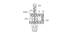
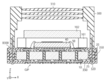
- a glass substrate having fastening holes, wiring layers provided on the first and second surfaces, a semiconductor chip provided above the glass substrate, a housing provided around the semiconductor chip, and a housing.
- the provided lens and a fastener for fastening the glass substrate and the housing through the fastening hole are provided.
- the fastening hole is larger than the outer edge of the head of the fastener.
- a filler may be further provided to fill the space between the fastener and the fastening hole.
- the fastening hole may be connected to the outside on the side surface of the glass substrate.
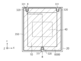
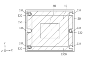
- a plurality of fastening holes are provided on the glass substrate, and the centers of gravity of the plurality of fastening holes may overlap the semiconductor chip in a plan view from the fastening direction.
- the fastener may be fastened to the housing and the glass substrate so that the optical axis of the lens and the optical axis of the semiconductor chip are substantially aligned with each other.
- the glass substrate may have a through hole penetrating between the first surface and the second surface, provided in the through hole, connected to any of the wirings, and further provided with electronic components.
- the frame may have a through hole penetrating between the third surface and the fourth surface, provided in the through hole, connected to any of the wirings, and further provided with electronic components.
- the glass substrate may have a counterbore provided on the first surface, be provided in the counterbore, be connected to any of the wirings, and further include electronic components.
- the frame has a counterbore provided on the third surface, may be provided in the counterbore, connected to any of the wirings, and further provided with electronic components.
- a plurality of electronic components having different thicknesses are provided in the through holes, and the surfaces of the plurality of electronic components may be aligned on the first surface.
- a plurality of electronic components having different thicknesses are provided in the through holes, and the surfaces of the plurality of electronic components may be aligned on the first surface.
- a plurality of electronic components having different thicknesses are provided in each of a plurality of counterbore with different depths, and the surfaces of the plurality of electronic components may be aligned on the first surface.
- a plurality of electronic components having different thicknesses are provided in each of a plurality of counterbore with different depths, and the surfaces of the plurality of electronic components may be aligned on the first surface.
- the glass substrate has a through hole penetrating between the first surface and the second surface, is provided in the through hole, further includes a heat radiating member having the second through hole, and the electronic component has the second through hole. It may be provided inside.
- a heat radiating member provided in the through hole and having a second counterbore may be further provided, and the electronic component may be provided in the second counterbore.
- a glass frame having one end directly connected to the first surface of the glass substrate and provided so as to surround the periphery of the semiconductor chip, and a cover glass connected to the other end of the glass frame to cover the upper part of the semiconductor chip are further provided. May be good.
- a glass frame having one end directly connected to the first surface of the glass substrate and provided so as to surround the periphery of the semiconductor chip, and a cover glass connected to the other end of the glass frame to cover the upper part of the semiconductor chip are further provided. May be good.
- the glass frame and the cover glass may be integrally formed.
- the glass frame and the cover glass may be integrally formed.
- the glass frame and cover glass may be made of the same material as the glass substrate.
- the glass frame and cover glass may be made of the same material as the glass substrate.
- a light-shielding film provided on a part of the surface of the glass frame and the cover glass may be further provided.
- a light-shielding film provided on a part of the surface of the glass frame and the cover glass may be further provided.
- FIG. 6 is a schematic cross-sectional view showing a configuration example of a semiconductor device according to a modified example of the first embodiment.
- FIG. 6 is a schematic cross-sectional view showing a configuration example of GIP according to the second embodiment.
- FIG. 6 is a schematic cross-sectional view showing a configuration example of one end of the GIP according to the third embodiment.
- the schematic cross-sectional view which shows the structural example of the through silicon via of GIP by 3rd Embodiment.
- FIG. 8 is a schematic cross-sectional view showing a method of manufacturing GIP
- FIG. 9 is a schematic cross-sectional view showing a method of manufacturing GIP
- FIG. 10 is a schematic cross-sectional view showing a method of manufacturing GIP
- FIG. 11 is a schematic cross-sectional view showing a method of manufacturing GIP
- FIG. 12 is a schematic cross-sectional view showing a method of manufacturing GIP
- FIG. 13 is a schematic cross-sectional view showing a method of manufacturing GIP, following FIG. FIG.
- FIG. 14 is a schematic cross-sectional view showing a method of manufacturing GIP, following FIG.
- the cross-sectional view which shows an example of the manufacturing method of GIP of 2nd Embodiment.
- the cross-sectional view which shows the structural example of GIP of 4th Embodiment.
- FIG. 5 is a cross-sectional view showing an example of a boundary portion between an opening and a metal plate.
- FIG. 5 is a cross-sectional view showing an example of an application using GIP according to the above embodiment.
- FIG. 6 is a cross-sectional view showing another example of an application using GIP according to the above embodiment.
- FIG. 5 is a cross-sectional view showing a configuration example of a semiconductor device according to a fifth embodiment.
- FIG. 5 is a cross-sectional view showing a configuration example of a semiconductor device according to a sixth embodiment.
- FIG. 5 is a cross-sectional view showing a configuration example of a semiconductor device according to the seventh embodiment.
- FIG. 5 is a cross-sectional view showing a configuration example of a semiconductor device according to a modified example of the seventh embodiment.
- FIG. 5 is a cross-sectional view showing a configuration example of a semiconductor device according to the eighth embodiment.
- FIG. 5 is a cross-sectional view showing a configuration example of a semiconductor device according to a modified example of the eighth embodiment.
- FIG. 5 is a cross-sectional view showing a configuration example of a semiconductor device according to a ninth embodiment.
- FIG. 5 is a cross-sectional view showing a configuration example of a semiconductor device according to the tenth embodiment.
- FIG. 5 is a cross-sectional view showing a method of manufacturing a semiconductor device according to the tenth embodiment.
- FIG. 5 is a cross-sectional view showing a configuration example of a semiconductor device according to a modified example of the tenth embodiment.
- FIG. 5 is a cross-sectional view showing a configuration example of a semiconductor device according to the eleventh embodiment.
- FIG. 5 is a cross-sectional view showing a method of manufacturing a semiconductor device according to the eleventh embodiment.
- FIG. 2 is a cross-sectional view showing a configuration example of a semiconductor device according to the twelfth embodiment.
- the plan view which shows the structural example of the semiconductor device by 12th Embodiment.
- FIG. 5 is a cross-sectional view showing a configuration example of a semiconductor device according to the thirteenth embodiment.
- the cross-sectional view which shows the structural example of the semiconductor device by 14th Embodiment.
- FIG. 6 is a cross-sectional view showing a configuration example of a semiconductor device according to a modified example of the 14th embodiment.
- FIG. 5 is a cross-sectional view showing a configuration example of a semiconductor device according to the fifteenth embodiment.
- FIG. 5 is a cross-sectional view showing a configuration example of a semiconductor device according to the 16th embodiment.
- the cross-sectional view which shows the structural example of the semiconductor device by 17th Embodiment.
- FIG. 5 is a cross-sectional view showing a configuration example of a semiconductor device according to the eighteenth embodiment.
- FIG. 5 is a cross-sectional view showing an example of a semiconductor device according to the nineteenth embodiment.
- FIG. 2 is a cross-sectional view showing an example of a semiconductor device according to the twentieth embodiment.
- FIG. 5 is a cross-sectional view showing a configuration example of a semiconductor device according to a modified example of the twentieth embodiment.
- FIG. 5 is a cross-sectional view showing a configuration example of a semiconductor device according to another modification of the 20th embodiment. The figure which shows the example which used the embodiment which concerns on this technology as a CMOS image sensor.
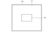
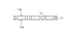
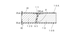
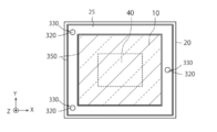
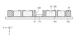
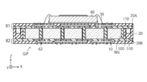
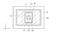
- FIG. 1 is a schematic plan view showing a configuration example of a semiconductor device (hereinafter, also referred to as a package or a module) according to the first embodiment.
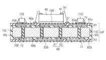
- FIG. 2 is a schematic cross-sectional view showing a configuration example of the semiconductor device according to the first embodiment. Note that FIG. 1 shows the positional relationship between the glass substrate 10, the insulating film 90c, and the semiconductor chip 40, and the detailed configuration of the through electrodes and the like is not shown.
- the semiconductor chip 40 is mounted on the central portion of the glass substrate 10.
- An insulating film 90c is provided around the glass substrate 10 so as to continuously cover the entire side surface of the glass substrate 10.
- the semiconductor chip 40 is not particularly limited, but may be, for example, a CMOS image sensor chip.
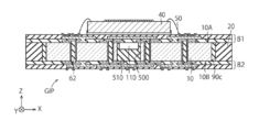
- the glass substrate 10 has a first surface 10A, a second surface 10B on the opposite side of the first surface, and a side surface (first surface) between the first surface 10A and the second surface 10B.
- Side surface Includes 10C.
- a laminated wiring portion 81 is provided on the first surface 10A.
- the laminated wiring portion 81 includes a plurality of layers of wiring 83a provided on the first surface 10A.
- the wiring 83a is covered with insulating films 85a and 90a.
- the laminated wiring portion 82 includes a plurality of layers of wiring 83b provided on the second surface 10B.
- the wiring 83b is covered with insulating films 85b and 90b.
- a low resistance metal material such as copper is used for example.
- a part of the wiring 83a is electrically connected to the electrode pad 71 on the first surface 10A.
- a part of the wiring 83b is electrically connected to the electrode pad 72 on the second surface 10B.
- the electrode pads 71 and 72 are connected to an electronic component 110 or the like, or are connected to another substrate or component (not shown).
- the other part of the wiring 83a is electrically connected to the bonding pad 51, and is electrically connected to the semiconductor chip 40 via the bonding pad 51 and the bonding wire 50.
- a part of the wiring 83a is provided on the first surface 10A of the glass substrate 10 so as to be in direct contact with the glass substrate 10, and an insulating film 90a is provided so as to cover a part of the wiring 83a. ..
- the insulating film 90a as the first insulating film covers the first surface 10A and the wiring 83a, a part of which is in contact with the first surface 10A, and the other portion is in contact with the wiring 83a. ..
- the wiring 83a that comes into direct contact with the glass substrate 10 can be used as an alignment mark in the subsequent process. In this case, it is not necessary to use the outer edge of the glass substrate 10 as the alignment mark. Therefore, the patterning of the laminated wiring portions 81 and 82 or the mounting of the semiconductor chip 40 can be performed with higher accuracy.
- a part of the wiring 83b is provided on the second surface 10B of the glass substrate 10 so as to be in direct contact with the glass substrate 10, and an insulating film 90b is provided so as to cover a part of the wiring 83b. ..
- the insulating film 90b as the second insulating film covers the second surface 10B and the wiring 83b, a part of which is in contact with the second surface 10B, and the other portion is in contact with the wiring 83b. ..
- An insulating film 90c is provided on the side surface 10C of the glass substrate 10. As shown in FIG. 1, the insulating film 90c as the third insulating film is provided on the entire outer circumference of the glass substrate 10. Further, as shown in FIG. 2, the insulating film 90c is provided so as to cover the entire side surface 10C from the first surface 10A to the second surface 10B.
- the insulating film 90c is continuous with at least one of the insulating films 90a and 90b, and is seamlessly connected. Alternatively, the insulating films 90a to 90c may be continuously and seamlessly connected to the entire first surface 10A, second surface 10B, and first side surface 10C.
- an insulating resin material such as an epoxy resin is used, and the insulating films 90a to 90c are made of the same material.
- the insulating film 90c covers the side surface 10C of the glass substrate 10 and is continuously connected to at least one of the insulating films 90a and 90b to protect the first surface 10A or the second surface 10B of the glass substrate 10. There is. Thereby, the insulating films 90a to 90c can protect the end portion and the side surface 10C of the glass substrate 10.
- the side surface 10C of the glass substrate 10 is substantially flat.
- the insulating film 90c is also substantially flat. As a result, the thickness of the insulating film 90c becomes substantially uniform, and stress concentration on the glass substrate 10 can be suppressed.
- the glass substrate 10 is provided with a through electrode 60.
- the through silicon via 60 includes a metal film 61 that covers the inner wall of a through hole (TGV (Through Glass Via)) that penetrates between the first surface 10A and the second surface 10B of the glass substrate 10, and the inside of the metal film 61. It has an insulating film 62 to be filled in.
- a low resistance metal material such as copper is used.
- the metal film 61 is continuously connected to the wirings 83a and 83b, and is preferably made of the same material as the wirings 83a and 83b.
- the metal film 61 is provided to electrically connect a part of the wiring 83 and a part of the wiring 84 via vias.
- the insulating film 62 as the fourth insulating film is continuously connected to the insulating films 90a and 90b, and is preferably made of the same material as the insulating films 90a to 90c. That is, for the insulating film 62, for example, an insulating material such as an epoxy resin is used. As a result, the insulating films 90a to 90c and 62 can be formed at the same time in the same process, and can be seamlessly configured as a continuous insulating film.
- the wiring layers 83a and 83b and the metal film 61 are seamlessly coated from the inner wall of the via to the periphery of the opening end, and the insulating films 90a to 90c and 62 are seamlessly and continuously filled from the inside to the outside of the via. Therefore, the stress generated on the TGV machined surface can be reduced and the TGV can be reinforced, and the TGV strength can be improved.
- a wiring 83a and an insulating film 85a are further provided on the insulating film 90a on the first surface 10A of the glass substrate 10.
- the laminated wiring portion 81 has a multilayer wiring structure.
- a wiring 83b and an insulating film 85b are further provided on the insulating film 90b on the second surface 10B of the glass substrate 10.
- the laminated wiring portion 82 also has a multilayer wiring structure.
- An electrode pad 71 and a bonding pad 51 are connected to the wiring 83a, and an electrode pad 72 or a bonding pad (not shown) is connected to the wiring 83b.
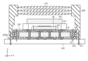
- a semiconductor chip 40 and an electronic component 110 are mounted on the glass substrate 10.
- the bonding pad 41 of the semiconductor chip 40 is connected to the bonding pad 51 via the bonding wire 50.
- the electronic component 110 is connected to the electrode pad 71.
- the semiconductor chip 40 is adhered on the insulating film 85a by the adhesive 100.
- this embodiment may be configured as a glass interposer (hereinafter, also simply referred to as GIP) on which the semiconductor chip 40 and the electronic component 110 are not yet mounted.
- GIP glass interposer
- the insulating film 90c covers the side surface 10C of the glass substrate 10 and is continuous with at least one of the insulating film 90a on the first surface 10A or the insulating film 90b on the second surface 10B of the glass substrate 10. Are connected. Thereby, the insulating films 90a to 90c can protect the end portion and the side surface 10C of the glass substrate 10.
- the laminated wiring portion 81 and the laminated wiring portion 82 are similarly layered, and have the same number of layers of the wiring layer and the same number of layers of the insulating layer. Further, it is preferable that the thickness of each wiring layer and the thickness of each insulating layer are substantially equal in the laminated wiring portion 81 and the laminated wiring portion 82. Therefore, the laminated wiring portion 81 and the laminated wiring portion 82 have a substantially symmetrical configuration, and substantially the same stress is applied to the glass substrate 10. Thereby, the distortion of the glass substrate 10 can be suppressed.
- the wiring patterns of the laminated wiring portion 81 and the laminated wiring portion 82 may be different.
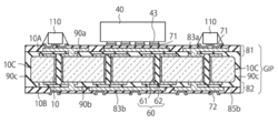
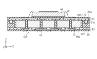
- FIG. 3 is a schematic cross-sectional view showing a configuration example of a semiconductor device according to a modified example of the first embodiment.
- the semiconductor chip 40 is flip-chip connected to a substrate for a semiconductor device.
- the semiconductor chip 40 has a metal bump 43 and is connected to the laminated wiring portion 81 by the metal bump 43. That is, in this modification, the semiconductor chip 40 is flip-chip connected above the glass substrate 10.
- Other configurations of this modification may be the same as the corresponding configurations of the first embodiment. Therefore, this modification can obtain the same effect as that of the first embodiment.
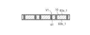
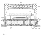
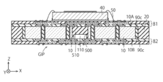
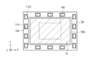
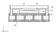
- FIG. 4 is a schematic plan view showing a configuration example of GIP according to the second embodiment.
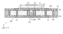
- FIG. 5 is a schematic cross-sectional view showing a configuration example of GIP according to the second embodiment.
- the GIP of the second embodiment may be applied to either the first embodiment or a modification thereof.
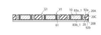
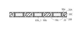
- the GIP of the second embodiment further includes a frame 20 on the side surface 10C of the glass substrate 10 and outside the insulating film 90c.
- the frame 20 is a frame-shaped member provided so as to face the entire side surface 10C over the outer periphery of the glass substrate 10.
- the frame 20 is adhered by an insulating film 90c on the side surface 10C of the glass substrate 10.
- the frame 20 has a third surface 20A, a fourth surface 20B, and a side surface (second side surface) 20C between the third surface 20A and the fourth surface 20B.
- the side surface 20C is an inner side surface of the frame 20 and is a surface facing the side surface 10C.
- the frame 20 is adhered to the insulating film 90c on the side surface 20C.
- the frame 20 is provided so as to surround the entire outer edge of the glass substrate 10, and protects the side surface 10C of the glass substrate 10 together with the insulating film 90c.
- the third surface 20A of the frame 20 is a frame surface on the first surface 10A side of the glass substrate 10.
- the fourth surface 20B of the frame 20 is a frame surface on the second surface 10B side of the glass substrate 10.
- the insulating film 90c is provided between the side surface 10C of the glass substrate 10 and the side surface 20C of the frame 20.
- the frame 20 is made of a material having a linear expansion coefficient close to that of the glass substrate 10.
- an insulating resin material such as glass epoxy resin is used.
- a first metal film 92a and a second metal film 92b are formed on the third surface 20A and the fourth surface 20B of the frame 20.
- the metal films 92a and 92b are formed by depositing a metal film on the surface of the frame 20 by a plating method and then patterning the metal film by using a lithography technique or the like.
- insulating films 90a, 90b, 85a and 85b are provided on the metal films 92a and 92b.
- the insulating film 90a is continuously provided from the first surface 10A of the glass substrate 10 to the metal film 92a.
- the insulating film 90b is continuously provided from the second surface 10B of the glass substrate 10 to the metal film 92b.
- the insulating film 85a is provided on the insulating film 90a, and is continuously provided from above the first surface 10A of the glass substrate 10 to above the metal film 92a.
- the insulating film 85b is provided on the insulating film 90b, and is continuously provided from above the second surface 10B of the glass substrate 10 to above the metal film 92b.
- the second embodiment can obtain the same effect as the first embodiment.
- the frame 20 is provided on the outside of the insulating film 90c along the side surface 10C of the glass substrate 10. Thereby, in the second embodiment, the end portion and the side surface 10C of the glass substrate 10 can be more reliably protected.
- this GIP when used for a CMOS image sensor, stray light can be blocked by the frame 20 covering the side surface 10C.
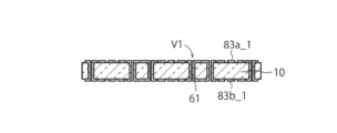
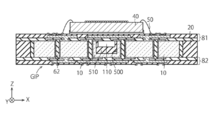
- FIG. 6 is a schematic cross-sectional view showing a configuration example of one end of the GIP according to the third embodiment.
- the side surface 10C of the glass substrate 10 has a curved surface shape that projects outward in a cross section in the direction perpendicular to the first surface 10A. This is because the dicing is performed using a laser and wet etching when the GIP is fragmented. Wet etching is performed by irradiating the glass substrate 10 with a short pulse laser in the thickness direction to modify it.
- the modified portion is selectively etched, and the corners of the side surface 10C of the glass substrate 10 are rounded due to the difference in exposure time to the etching solution, and the side surface 10C is formed into a curved surface shape protruding outward. As a result, stress concentration and microcracks that cause chipping and cracking at the edges of the glass substrate 10 can be reduced.
- FIG. 7 is a schematic cross-sectional view showing a configuration example of the through silicon via of the GIP according to the third embodiment.
- the inner side surface of the via V1 of the through electrode 60 may also have a curved surface shape as in the side surface 10C.
- the via V1 of the through electrode 60 is formed by laser and wit etching as in dicing, the inner surface of the via V1 projects inward of the via V1 in a cross section perpendicular to the first surface 10A. It has a curved shape. That is, the corners of the via V1 provided on the glass substrate 10 are rounded, and when viewed from the glass substrate 10, the via V1 is formed into a curved surface shape protruding outward from the glass substrate 10. As a result, it is possible to further suppress chipping and cracking of the end portion of the glass substrate 10 in the through electrode 60.
- the curvature of the curved surface of the inner surface of the through electrode 60 is substantially equal to the curvature of the curved surface of the side surface 10C. That is, the cross-sectional shape of the inner surface of the through electrode 60 is substantially the same as the cross-sectional shape of the side surface 10C. In this case, it is not necessary to separately prepare the process recipes for dicing and via formation, and the process can be simplified.
- FIG 8 to 15 are schematic cross-sectional views showing an example of the GIP manufacturing method of the first embodiment.
- the glass substrate 10 has a first surface 10A and a second surface 10B.
- the glass substrate 10 has not yet been diced and does not have the first side surface 10C at this stage. That is, the glass substrate 10 is in a glass panel state at this stage.
- via V1 is formed as a through hole (TGV) penetrating the glass substrate 10 between the first surface 10A and the second surface 10B.
- the via V1 is formed at the position of the through electrode 60.
- the via V1 is formed using, for example, laser processing technology and etching technology.
- a series of modified points arranged in the thickness direction of the glass substrate 10 is formed by laser light, and then the glass substrate 10 is somewhat etched by wet etching.
- the inner side surface of the via V1 is rounded into a curved surface shape, and chipping or cracking of the end portion of the through electrode 60 can be suppressed.
- a metal film is formed on the inner wall surfaces of the first surface 10A, the second surface 10B, and the via V1.
- the metal film is made of a low resistance metal such as copper and is formed by plating.
- the metal film 83a_1 which is the lower layer of the wiring 83a is formed on the first surface 10A
- the metal film 83b_1 which is the lower layer of the wiring 83b is formed on the second surface 10B.
- a metal film 61 is formed on the inner wall surface of the via V1.
- the wirings 83a and 83b and the metal film 61 are in direct contact with the surface of the glass substrate 10.
- the metal films 83a_1 and 83b_1 are processed into a predetermined wiring pattern.
- the metal films 83a_1 and 83b_1 may be patterned by using a laser processing technique.
- the metal films 83a_1 and 83b_1 may be patterned using a lithography technique and an etching technique.
- the wiring 83a that comes into direct contact with the first surface 10A of the glass substrate 10 can be used as an alignment mark.
- the patterning of the laminated wiring portions 81 and 82 can be performed with higher accuracy.
- the glass plate-shaped glass substrate 10 is diced and individualized so as to be suitable for each semiconductor device.
- dicing for example, laser processing technology and etching technology may be used as in the case of via V1.
- the glass substrate 10 is diced with a laser beam, and then the glass substrate 10 is somewhat etched using wet etching.
- the side surface 10C of the glass substrate 10 has a curved surface shape that projects outward. As a result, it is possible to suppress chipping and cracking of the end portion of the glass substrate 10.
- each piece of glass substrate 10 is arranged in the frame 20 on the support substrate.
- Metal films 92a and 92b are provided in advance on the third surface 20A and the fourth surface 30B of the frame 20.
- the frame 20 is formed in a mesh shape, and individual glass substrates 10 are placed inside the mesh.
- the inner side surface 20C of the frame 20 faces the side surface 10C of the glass substrate 10, and a gap G1 is provided between the side surface 20C and the side surface 10C.
- the gap G1 may have a width that allows the material of the insulating film 90c to be poured and can absorb the stress generated from the deformation difference between the glass substrate 10 and the frame 20, and is as small as possible in order to reduce the package size of the semiconductor device. The narrower one is preferable.
- a resin material is laminated on the first surface 10A of the glass substrate 10 and the third surface 20A of the frame 20.
- the resin material is in the form of a film and can flow by heating. Therefore, the resin material also flows into the via V1 and also into the gap G1 between the side surface 20C of the frame 20 and the side surface 10C of the glass substrate 10.
- the insulating film 90a is formed on the first surface 10A, the insulating film 62 is filled inside the metal film 61 in the via V1, and the insulating film 90c is filled in the gap G1.
- the resin material flows into the via V1 and the gap G1 and then is temporarily cured by heat treatment.
- the insulating film 90a covers the metal film 83a_1 on the first surface 10A and protects the metal film 83a_1. Further, the insulating film 90c is filled in the gap G1 to fix the frame 20 to the glass substrate 10.
- the insulating film 62 protects the metal film 61 by filling the via V1. The metal film 61 and the insulating film 62 form a through electrode 60 in the via V1.
- the metal film 83a_1 is not provided above the opening of the via V1 and is open. This is because the metal film 83a_1 is prevented from closing the opening of the via V1 so that the resin material can flow into the via V1.
- the metal film 83b_1 is not provided below the opening of the via V1 and is open. This is because the metal film 83b_1 is prevented from closing the opening of the via V1 on the second surface 10B side, and the resin material can flow into the via V1 from the second surface 10B side. As a result, the glass substrate 10 in the vicinity of the via V1 can be strengthened in terms of strength. Therefore, in order to pour the resin material into the via V1, the metal films 83a_1 and 83b_1 are not provided above or below the opening of the via V1.
- the insulating films 90a, 90c, 62 are formed in the same process using the same resin material (for example, epoxy resin or the like). Therefore, the insulating films 90a, 90c, 62 can be formed as seamlessly continuous insulating films. Thereby, the insulating films 90a, 90c, 62 and the frame 20 can surely protect the glass substrate 10.
- the resin material is laminated from the second surface 10B side of the glass substrate 10. It is preferable that the resin material is sufficiently filled in the via V1 and the gap G1 from the first surface 10A, and in this case, it is sufficient that the resin material is laminated on the second surface 10B. After that, the resin material is temporarily cured. As a result, the insulating film 90b is formed on the second surface 10B. The insulating film 90b is formed after the insulating films 90a, 90c, and 62, and is formed individually. At this point, the insulating film 90b and the insulating films 90a, 90c, 62 are in a temporarily cured state. After that, it is finally cured by further heating.
- the insulating film 90b and the insulating films 90a, 90c, 62 are made of the same material, and the joint portion can be melted during the main curing to be formed almost seamlessly and continuously. As a result, the end portion of the glass substrate 10 can be protected, and the stress applied to the glass substrate 10 is also reduced. Further, the insulating films 90a and 90b are less likely to be peeled off from the glass substrate 10.
- the effect of the present embodiment is not lost even if there is a joint between them. That is, if the insulating film 90c is continuously connected to at least one of the insulating films 90a and 90b, at least one end of the glass substrate 10 is protected, and the glass substrate 10 can be protected from stress.
- the insulating films 90a and 90b are processed into a predetermined pattern to expose a part of the metal films 83a_1 and 83b_1.
- the insulating films 90a and 90b may be via-processed by using a laser processing technique.
- the insulating films 90a and 90b may be patterned using a lithography technique and an etching technique.
- the metal film 83a_2 which is the upper layer of the wiring 83a, is deposited and patterned on the insulating film 90a and the metal film 83a_1. Further, the insulating film 85a is deposited and patterned on the metal film 83a_2. In this way, the laminated wiring portion 81 is formed by repeating the deposition and processing of the metal film 83a_2 and the insulating film 85a.
- the metal film 83b_2 which is the upper layer of the wiring 83b, is deposited and patterned on the insulating film 90b and the metal film 83b_1. Further, the insulating film 85b is deposited and patterned on the metal film 83b_2. In this way, the laminated wiring portion 82 is formed by repeating the deposition and processing of the metal film 83b_2 and the insulating film 85b.
- the number, film thickness and material of the metal films 83a_1, 83a_2 and the insulating films 90a and 85a on the first surface 10A side of the glass substrate 10 are the layers of the metal films 83b_1, 83b_2 and the insulating films 90b and 85b on the second surface 10B side. It is preferably approximately equal in number, film thickness and material. As a result, the stress applied to the glass substrate 10 from the laminated wiring portions 81 and 82 becomes substantially equal, and the distortion of the glass substrate 10 can be suppressed.
- the GIP including the glass substrate 10 is separated by dicing between the frame 20 and the insulating film 90c.
- Dicing may be performed using a laser processing technique or a dicing blade.
- dicing is performed between the side surface 20c of the frame 20 and the side surface 10C of the glass substrate 10.
- the insulating film 90c remains on the side surface of the glass substrate 10, but the frame 20 is not left.
- the GIP shown in FIG. 2 or 3 can be formed.
- the semiconductor chip 40 is adhered on the insulating film 85a, and the bonding wire 50 is connected between the bonding pad 41 of the semiconductor chip 40 and the bonding pad 51 of the laminated wiring portion 81. Further, the electronic component 110 is connected to the electrode pad 71. As a result, the structure shown in FIG. 2 is obtained.
- the semiconductor chip 40 may be flip-chip connected on the GIP.
- the semiconductor chip 40 has a metal bump 43 and is connected to the laminated wiring portion 81 by the metal bump 43. In this way, the semiconductor chip 40 may be flip-chip connected above the glass substrate 10. As a result, the structure shown in FIG. 3 is obtained.
- CMOS image sensor module or the like can be formed by further undergoing an assembly process.
- FIG. 16 is a cross-sectional view showing an example of the GIP manufacturing method of the second embodiment.
- the frame 20 is diced as shown in FIG.
- the glass substrate 10 including the insulating film 90c and the frame 20 is separated into pieces.
- Dicing may be performed using a laser processing technique or a dicing blade. Dicing is performed along the center line of the frame 20 or both sides thereof.
- the insulating film 90c and the frame 20 are left on the side surface of the glass substrate 10.
- the GIP shown in FIG. 5 can be formed.
- the semiconductor chip 40 is adhered on the insulating film 85a, and the bonding wire 50 is connected between the bonding pad 41 of the semiconductor chip 40 and the bonding pad 51 of the laminated wiring portion 81.
- the semiconductor chip 40 may be flip-chip connected on the GIP.
- CMOS image sensor module or the like can be formed by further undergoing an assembly process.
- the glass substrate 10 in a plate state is individualized before the insulating films 90a to 90c, 85a and 85b are deposited on the glass substrate 10.
- the stress due to the curing shrinkage of the insulating films 90a to 90c, 85a and 85b is dispersed.
- the stress generated on the side surface 10C can be reduced.
- the stress of the GIP glass substrate 10 manufactured according to the first embodiment was about half the stress of the glass substrate that was separated after the laminated wiring portions 81 and 82 were formed.
- the stress of the glass substrate 10 of the GIP provided with the frame 20 manufactured by the second embodiment became about 1/7 of the stress of the glass substrate that was separated after the formation of the laminated wiring portions 81 and 82. ..
- FIG. 17 is a cross-sectional view showing a configuration example of the GIP of the fourth embodiment.
- the GIP according to the fourth embodiment has an opening 11 at the center of the glass substrate 10.
- the opening 11 is provided in the central portion of the glass substrate 10 between the first surface 10A and the second surface 10B, and has a taper on the inner side surface.
- a metal plate 120 is fitted in the opening 11.
- the metal plate 120 is provided on the back surface side of the semiconductor chip 40, absorbs the heat generated in the semiconductor chip 40, and releases the heat from the second surface 10B side of the glass substrate 10. That is, the metal plate 120 functions as a heat sink of the semiconductor chip 40.
- a highly thermally conductive material such as copper or silicon is used.
- the side surface of the metal plate 120 has a taper having an inclination substantially equal to the inner side surface of the opening 11 so as to be along the inner surface of the opening 11.
- An insulating film 65 is provided between the side surface of the metal plate 120 and the inner surface surface of the opening 11. Like the insulating films 62 and 90c, the insulating film 65 is formed by filling the resin material between the side surface of the metal plate 120 and the inner surface of the opening 11 at the same time as forming the insulating film 90a. Therefore, the insulating film 65 extends in a direction inclined with respect to the first and second surfaces 10A and 10B along the side surface of the metal plate 120 and the inner surface surface of the opening 11.
- the insulating film 65 is made of the same material as the insulating films 90a, 90c, 62, and is continuously and seamlessly connected to the insulating films 90a, 90c, 62. As a result, the insulating film 65 can sufficiently protect the end portion of the opening 11 of the glass substrate 10.
- the insulating film 65 is made of the same material as the insulating film 90b, and may be continuously and seamlessly connected. As a result, the insulating film 65 can more reliably protect the end portion of the opening 11 of the glass substrate 10. In addition, the stress on the glass substrate 10 is also reduced.
- the fourth embodiment is effective when the stress applied to the glass substrate 10 differs between the first surface 10A and the second surface 10B due to differences in the film thickness, the number of layers, the material, etc. of the laminated wiring portions 81 and 82. be.
- FIG. 18 is a cross-sectional view showing an example of a boundary portion between the opening 11 and the metal plate 120. It is assumed that the laminated wiring portion 81 is 20 ⁇ m, the laminated wiring portion 82 is 30 ⁇ m, and the insulating film 65 is 100 ⁇ m.
- the laminated wiring portions 81 and 82 each include a metal film having the same pattern and an insulating film having the same pattern, each having the same thickness.
- FIG. 19 is a graph showing the results of warpage analysis of the glass substrate 10 shown in FIG.
- the inclination angle ⁇ of the taper is the inclination angle of the inner wall surface of the opening 11 on the glass substrate 10 side with respect to the second surface 10B having the relatively thick laminated wiring portion 82.
- the warp is minimized when the inclination angle ⁇ is about 75 degrees. That is, if the inclination angle ⁇ of the taper of the opening 11 and the metal plate 120 is set to about 75 degrees, the warp applied to the glass substrate 10 is minimized.
- the side surface of the metal plate 120 and the inner side surface of the opening 11 are tapered, and the insulating film 65 is filled along the taper. Thereby, the warp generated in the glass substrate 10 can be controlled and reduced.
- the fourth embodiment may be the same as the corresponding configurations of the first embodiment. Therefore, the fourth embodiment can obtain the same effect as the first embodiment. Further, the fourth embodiment may be applied to either the second or third embodiment.
- a part of the laminated wiring portions 81 and 82 or the metal films 92a and 92b may be used as an antenna for wireless communication.
- FIG. 20 is a cross-sectional view showing an example of an application using GIP according to the above embodiment.
- the GIP may be any of the above-mentioned first to fourth embodiments or a modification thereof.
- the semiconductor chip 40 is a CMOS image sensor chip, and the light receiving surface is directed upward.
- the semiconductor chip 40 is adhered on the GIP with an adhesive, and is electrically connected to a part of the wiring of the GIP by the bonding wire 50.
- a fixed frame 101 is arranged around the semiconductor chip 40.
- the fixing frame 101 is provided to fix the cover glass 102 at a predetermined position above the light receiving surface of the semiconductor chip 40.
- the cover glass 102 protects the light receiving surface of the semiconductor chip 40 and allows incident light to pass through the light receiving surface.
- the cover glass 102 may be a condenser lens.
- the GIP according to the present embodiment can be used as a substrate of the CMOS image sensor.
- FIG. 21 is a cross-sectional view showing another example of the application using GIP according to the above embodiment.
- the GIP is basically any of the above-mentioned first to fourth embodiments or a modification thereof.
- the CMOS image sensor chip 40, the signal processing chip 103, the power amplifier 104, and the antenna 105 are mounted on one GIP and are configured as one module. Therefore, the GIP has a relatively large size.
- the metal plate 120 is embedded in the GIP below the CMOS image sensor chip 40. Below the power amplifier 104, a metal plate 121 is embedded in the GIP.
- the arrangement of the semiconductor chip 40, the fixed frame 101, and the cover glass 102 is the same as in Application Example 1.
- a metal plate 120 is fitted in the lower portion of the opening 11. In this way, the metal plate 120 is provided in the opening 11, and the semiconductor chip 40 is provided on the metal plate 120.
- the metal plate 120 is in contact with the back surface of the semiconductor chip 40 via the wiring 83a and the metal pad 71, absorbs the heat generated in the semiconductor chip 40, and transfers the heat to the second surface 10B side of the glass substrate 10. Emit from.
- the material of the wiring 83a and the metal pad 71 is interposed between the metal plate 120 and the semiconductor chip 40. Further, materials for the wiring 83b and the metal pad 72 are provided on the second surface 10B side of the metal plate 120.
- the materials of the wirings 83a and 83b and the metal pads 71 and 72 are provided for the heat dissipation path.
- the signal processing chip 103 is provided on the second surface 10B side and is electrically connected to the electrode pad 72.
- the signal processing chip 103 performs arithmetic processing on a pixel signal that has been photoelectrically converted and AD-converted by the semiconductor chip 40.
- GIP has an opening 111 in addition to the opening 11.
- the metal plate 121 is fitted in the opening 111.
- the power amplifier 104 is provided under the metal plate 121 in order to amplify a signal or the like received by the antenna 105. In this way, the metal plate 121 is provided in the opening 111.
- the metal plate 121 is in contact with the back surface of the power amplifier 104 via the wiring 83b and the metal pad 72, absorbs the heat generated in the power amplifier 104, and transfers the heat to the first surface 10A side of the glass substrate 10. Emit from.
- the material of the wiring 83b and the metal pad 72 is interposed between the metal plate 121 and the power amplifier 104.
- the material of the wiring 83a and the metal pad 71 is provided on the first surface 10A side of the metal plate 121.
- the materials of the wirings 83a and 83b and the metal pads 71 and 72 are provided for the heat dissipation path.
- the antenna 105 is provided on the first surface 10A side of the GIP.
- the antenna 105 is provided to receive an external signal and transmit an internal signal.
- the antenna 105 is configured by providing a metal wiring 105a that functions as an antenna element on a glass substrate.
- GIP is characterized by low power loss of high frequency signals. Therefore, it is advantageous to mount, for example, an antenna for 5G as in Application Example 2.
- the GIP according to the present embodiment can also be used as the substrate of the module of the CMOS image sensor.
- the semiconductor device according to the present embodiment is advantageous in terms of space saving and low power loss.
- the insulating film Before forming the metal films 83a_1, 83b_1, 61, the insulating film may be formed in the first surface 10A, the second surface 10B, and the via V1 of the glass substrate 10.
- an insulating material such as an epoxy resin may be used.
- metal films 83a_1, 83b_1, 61 are formed on the surface of the insulating film in the first surface 10A, the second surface 10B, and the via V1 of the glass substrate 10.
- the metal films 83a_1, 83b_1, 61 are processed by using the laser processing technique.
- the glass substrate 10 is separated into pieces by the dicing process.
- the glass substrate 10 is arranged on the frame 20, and the wiring layers 81 and 82 are formed.
- the metal films 83a_1, 83b_1, 61 are formed on the insulating film without directly contacting the glass substrate 10.
- the insulating films 90a and 90b can seamlessly and continuously cover the first surface 10A, the second surface 10B, and the side surface 10C of the glass substrate 10. Therefore, the first modification can obtain the effect of the first embodiment.
- the insulating film may be formed on the metal films 83a_1, 83b_1, 61 before the dicing step.
- an insulating film is formed on the metal films 83a_1, 83b_1, 61.
- the insulating film is also embedded in the via V1 and also covers the metal film 61.
- the glass substrate 10 is fragmented by the dicing process.
- the glass substrate 10 is arranged on the frame 20, and the wiring layers 81 and 82 are formed.
- the insulating films 90a and 90b embedded between the frame 20 and the glass substrate 10 are different from the insulating films covering the metal films 83a_1, 83b_1 and 61 and are not continuous.
- the insulating films 90a and 90b can seamlessly and continuously cover the first surface 10A, the second surface 10B, and the side surface 10C of the glass substrate 10. Therefore, in the second modification, the effect of the first embodiment can be obtained.
- FIG. 22 is a cross-sectional view showing a configuration example of the semiconductor device according to the fifth embodiment.
- the GIP glass substrate 10 is fastened to the housing 300 provided with the lens group 310 by screws 320 as fasteners.
- the glass substrate 10 is provided with a fastening hole 330 for passing the screw 320 through.
- the fastening hole 330 is provided so as to penetrate the glass substrate 10 between the first surface 10A and the second surface 20B.
- a filler 340 is filled between the fastening hole 330 and the screw 320.
- the screw 320 penetrates the filler 340 in the fastening hole 330 and is fastened to the housing 300 to fix the glass substrate 10 to the housing 300.
- an insulating material such as resin is used for the filler 340.
- the frame 20 is adhered to the side surface of the glass substrate 10 with an adhesive 350.
- the housing 300 has a substantially rectangular tubular shape so as to surround the semiconductor chip 40.
- a lens group 310 is provided above the semiconductor chip 40 of the housing 300. The light that has passed through the lens group 310 is incident on the semiconductor chip 40 as a CIS or the like.
- the fastening hole 330 can be formed by irradiating a laser beam to alter the glass substrate 10 and etching the altered portion with a hydrofluoric acid solution or the like. Alternatively, the fastening hole 330 may be formed by scraping the glass substrate 10 using laser ablation.
- the GIP is directly fastened to the housing 300, and the end portion of the housing 300 is arranged on the GIP and is in contact with the GIP.
- the GIP can be fastened to the housing 300 without impairing the characteristics of the glass substrate 10, such as high flatness, small warpage, and small tilt.
- the contact surface B300 between the housing 300 and the GIP serves as an optical axis reference surface between the optical axis of the lens group 310 and the optical axis of the semiconductor chip 40.
- the optical axis reference plane is a contact surface having a large influence because the optical axis of the lens group 310 and the optical axis of the semiconductor chip 40 are substantially aligned with each other.
- the optical axis of the lens group 310 and the optical axis of the semiconductor chip 40 are processed by processing the surfaces of the housing 300 and the GIP facing the contact surface B300 with high accuracy. Can be almost matched with.
- the configuration of the GIP, the fixed frame 101, the cover glass 102, and the semiconductor chip 40 may be the same as that of either the above embodiment or the above modification.
- the GIP, the semiconductor chip 40, and the lens group 310 may be configured as an integrated module.
- this module can be incorporated into a product such as a camera while keeping the optical axes of the semiconductor chip 40 and the lens group 310 substantially aligned.
- FIG. 23 is a schematic plan view showing a configuration example of the semiconductor device according to the fifth embodiment.
- the plane layout of the fastening hole 330 will be described with reference to FIG. 23.
- FIG. 22 is a cross section taken along the line AA of FIG. 23.
- three fastening holes 330 are provided in the glass substrate 10.
- the fastening hole 330 is provided in the contact surface B300 between the housing 300 and the GIP.
- the fastening holes 330 are unevenly arranged on one side of the glass substrate 10, resonance or abnormal vibration may be induced when micro-vibration propagates to the GIP. In this case, vibration may propagate to the semiconductor chip 40 and components mounted on the GIP and cause damage.
- the plurality of fastening holes 330 are arranged so that their centers of gravity are in the semiconductor chip 40 (overlapping) in the plane layout viewed from the Z direction. By arranging the fastening holes 330 substantially evenly in this way, it is possible to suppress damage to the semiconductor chips 40 and components mounted on the GIP.
- the number of screws 320 and fastening holes 330 is not limited to three, and any number may be used as long as it is two or more. However, as described above, it is preferable that the screws 320 and the fastening holes 330 are arranged substantially evenly on the contact surface B300.
- FIG. 24 is a cross-sectional view showing a configuration example of the semiconductor device according to the sixth embodiment.
- the GIP glass substrate 10 is fastened to the mounting board 400 with screws 320, and the mounting board 400 is fastened to the housing 300 provided with the lens group 310 with screws 321 as fasteners. .. That is, the GIP is fixed to the housing 300 via the mounting board 400.
- the mounting board 400 is a wiring board in which a plurality of wiring layers 410 and a plurality of insulating layers 420 are laminated.
- a metal material such as copper is used.
- an insulating material such as a glass epoxy resin is used.
- the insulating layer 420 is provided in the region of the mounting board 400 that the housing 300 contacts, but the wiring layer 410 is not provided. As a result, the screw 321 can penetrate the mounting board 400 without contacting the wiring layer 410.
- the screw 321 penetrates the region of the insulating layer 420 of the mounting board 400 and is fastened to the housing 300.
- the configuration of the GIP itself may be the same as that of the fifth embodiment.
- the screw 320 penetrates the fastening hole 330 in the ⁇ Z direction and is fastened to the mounting substrate 400.
- the region of the mounting substrate 400 corresponding to the fastening hole 330 is also provided with the insulating layer 420, but is not provided with the wiring layer 410.
- the screws 320 can be fastened to the mounting board 400 without coming into contact with the wiring layer 410.
- the contact surface B300 between the housing 300 and the mounting substrate 400 serves as the optical axis reference surface.
- the semiconductor chip 40 mounted on the front surface of the GIP and the back surface of the GIP (that is, the front surface of the mounting substrate 400) are in a state where the parallelism is maintained. .. Therefore, by processing the surfaces of the housing 300 and the mounting substrate 400 facing the contact surface B300 with high accuracy, the optical axis of the lens group 310 and the optical axis of the semiconductor chip 40 can be substantially aligned with each other.
- the configuration of the GIP, the fixed frame 101, the cover glass 102, and the semiconductor chip 40 may be the same as that of either the above embodiment or the above modification.
- the GIP, the semiconductor chip 40, and the lens group 310 may be configured as an integrated module.
- this module can be incorporated into a product such as a camera while keeping the optical axes of the semiconductor chip 40 and the lens group 310 substantially aligned.
- FIG. 25 is a cross-sectional view showing a fastening portion of the fifth embodiment.
- the fastening hole 330 is provided on the contact surface B330 between the housing 300 and the GIP. Further, the width W330 of the fastening hole 330 is preferably larger than the width W320 of the head of the screw 320. That is, as shown in FIGS. 23 and 25, the fastening hole 330 is formed larger than the outer edge of the head of the screw 320 in a plan view seen from the Z direction (the fastening direction of the screw 320). As a result, the glass substrate 10 does not exist directly under the head of the screw 320, and the head of the screw 320 presses the filler 340 but does not directly press the glass substrate 10 at the time of fastening. As a result, it is possible to prevent the glass substrate 10 from being damaged by the load caused by fastening the screws 320. It is preferable that the relationship between the fastening hole 330 and the screw 320 of the sixth embodiment is the same.
- FIG. 26 is a cross-sectional view showing a configuration example of the semiconductor device according to the seventh embodiment.
- FIG. 27 is a schematic plan view showing a configuration example of the semiconductor device according to the seventh embodiment.
- FIG. 26 shows a cross section along line BB of FIG. 27.
- the fastening hole 330 is connected to the outside on the side surface of the glass substrate 10, and serves as a notch portion 331 for fastening.
- the notch portion 331 is a region recessed from the side surface of the glass substrate 10 toward the inside in the XY plane.
- a frame 20 is provided inside the recess of the notch 331.
- the frame 20 and the glass substrate 10 are adhered to each other by an adhesive 350.
- the screw 320 penetrates the frame 20 in the notch 331 and is fastened to the housing 300.
- the notch portion 331 may be formed in this way.
- the cutout portion 331 preferably has a smoothly continuous outer edge without having a corner, as shown in FIG. 27.
- the strength of the notch portion 331 can be maintained.
- the number of notch portions 331 is not limited to three, and may be any number of two or more. However, considering the strength of the glass substrate 10, it is preferable to reduce the number of notches 331 as much as possible and make the contact portion with the frame 20 as small as possible.
- the notch portions 331 are preferably arranged substantially evenly on the contact surface B300 between the GIP and the housing 300. Even with such a notch portion 331, the effect of the present disclosure is not lost.
- the fastening hole 330 and the notch 331 may be mixed.
- FIG. 28 is a cross-sectional view showing a configuration example of a semiconductor device according to a modified example of the seventh embodiment.
- the six notches 331 are arranged line-symmetrically or point-symmetrically with respect to the center line or the center of the glass substrate 10.
- the notch portion 331 can be provided without impairing the characteristics such as the flatness of the glass substrate 10.
- the screws 320 are fastened to the three notch portions 331 out of the six notch portions 331.
- the size of the notch 331 of the glass substrate 10 is preferably the same, but the size may be changed as necessary in consideration of the overall balance.
- the seventh embodiment and the present modification may be applied to the sixth embodiment.
- FIG. 29 is a cross-sectional view showing a configuration example of the semiconductor device according to the eighth embodiment.
- FIG. 30 is a plan view showing a configuration example of the semiconductor device according to the eighth embodiment.
- the frame 25 is provided between the side surface of the glass substrate 10 and the frame 20.
- the frame 25 as the second frame is provided directly below the housing 300, and is provided for fastening the GIP to the housing 300 with screws 320.
- a material other than glass is used for the frame 25.
- a metal material such as stainless steel is used when high rigidity is required, an aluminum alloy or titanium alloy is used when weight reduction is required, and a copper alloy or the like is used when high thermal conductivity is required. Is used.
- a fastening hole 330 through which the screw 320 is passed is provided in the frame 25.
- three fastening holes 330 are provided in the frame 25, but the number of fastening holes 330 is not limited. Further, it is preferable that the fastening holes 330 are arranged substantially evenly in the frame 25.
- the frame 25 is adhered to the side surface of the glass substrate 10 with an adhesive 350.
- the frame 20 is similarly adhered to the outer surface of the frame 25 with an adhesive 350.
- the frame 25 is configured as a part of the GIP, consideration must be given to bring the coefficient of linear expansion and the like closer to the glass substrate 10.
- the relationship between the linear expansion coefficients of the glass substrate 10, the frame 25, and the housing 300 is preferably glass substrate 10 ⁇ frame 25 ⁇ housing 300, or housing 300 ⁇ frame 25 ⁇ glass substrate 10.
- the coefficient of thermal expansion at the fastening portion from the glass substrate 10 to the housing 300 is configured to gradually change, so that the stress of the entire module is reduced.
- the frame 25 may also have a function of protecting the side surface of the glass substrate 10. In this case, the frame 20 may be omitted. However, this package is made into individual pieces through a dicing step of cutting the resin frame 20 in the manufacturing process. Therefore, when the frame 25 is made of a metal material or the like that cannot be diced, it is preferable that the frame 20 is provided in addition to the frame 25.
- FIG. 31 is a cross-sectional view showing a configuration example of a semiconductor device according to a modified example of the eighth embodiment.
- a heat radiating portion 360 that is fastened and contacts with a screw 320 is provided at the bottom of the GIP.
- the heat radiating portion 360 is fastened to the second surface 10B side of the glass substrate 10 by screws 320.
- the screw 320 fastens the heat radiating portion 360 to the GIP together with the fastening of the GIP and the housing 300.
- a material such as copper or aluminum is used as a material having high thermal conductivity.
- the heat of the housing 300 and the GIP can be exhausted from the heat radiating unit 360 via the screws 320 and the like.
- the heat of the GIP is transferred to the heat radiating unit 360 via the laminated wiring portions 81 and 82, and can be efficiently exhausted from the heat radiating unit 360.
- FIG. 32 is a cross-sectional view showing a configuration example of the semiconductor device according to the ninth embodiment.
- the GIP glass substrate 10 is fastened to the substrate 401 with screws 320, and the substrate 401 is fastened to the housing 300 including the lens group 310 with screws 321. That is, the GIP is fixed to the housing 300 via the substrate 401.
- the substrate 401 is a plate-shaped substrate having excellent heat dissipation, flatness, parallelism, and rigidity.
- the substrate 401 for example, copper, aluminum, tungsten, molybdenum, niobium, titanium, alloys containing these metals, and alloys such as stainless steel, duralumin, Invar, Kovar, and brass are used.
- the glass substrate 10 is fastened to the substrate 401 with screws 320 via the frame 25 and comes into close contact with the substrate 401.
- the substrate 401 is fastened to the housing 300 via the screws 321 and is brought into close contact with the housing 300, so that the rigidity and heat dissipation can be further improved.
- the screw 321 penetrates the substrate 401 and is fastened to the housing 300.
- the configuration of the GIP itself may be the same as that of the eighth embodiment.
- the screw 320 penetrates the frame 25 in the ⁇ Z direction and is fastened to the substrate 401.
- the substrate 401 and GIP may be fixed via an adhesive or the like having a high thermal conductivity.
- FIG. 33 is a cross-sectional view showing a configuration example of the semiconductor device according to the tenth embodiment.
- FIG. 34 is a schematic plan view showing a configuration example of the semiconductor device according to the tenth embodiment.
- the electronic component 110 is built in the glass substrate 10 of the GIP.
- a through hole (cavity) 500 is provided directly below the semiconductor chip 40 of the glass substrate 10, and the electronic component 110 is arranged in the through hole 500.
- the through hole 500 is provided at the center of the glass substrate 10 so as to penetrate the glass substrate 10 between the first surface 10A and the second surface 20B.
- the through hole 500 is formed to have a size capable of accommodating the electronic component 110.
- the space of the through hole 500 other than the electronic component 110 is filled with the insulating film 510.
- the insulating film 510 may be made of the same material as the insulating films 62 and 90c, and may be embedded in the space of the through hole 500 in the same process as the formation of the insulating films 62 and 90c.
- the through hole 500 can be formed by irradiating a laser beam to alter the glass substrate 10 and etching the altered portion with a hydrofluoric acid solution or the like.
- the through hole 500 may be formed by scraping the glass substrate 10 using laser ablation.
- the upper surface of the electronic component 110 is aligned with the first surface 10A of the glass substrate 10. Further, the electronic component 110 is connected to any of the wirings of the laminated wiring portion 81 on the first surface 10A side of the glass substrate 10. As a result, electric power can be supplied to the electronic component 110 from the outside via the wiring of the laminated wiring portion 81, a control signal can be given to the electronic component 110, or data can be output from the electronic component 110.
- Other configurations of the GIP of the tenth embodiment may be similar to the corresponding configurations of any of the above embodiments or modifications. In the tenth embodiment, the presence or absence of the frame 20 does not matter.
- the electronic component 110 may be, for example, either an active component or a passive component.
- the electronic component 110 is, for example, as an active component, DSP (Digital Signal Processor), DRAM (Dynamic Random Access Memory), SRAM (Static RAM), MRAM (Magnetoresistive RAM), FPGA (Field-Programmable Gate Array) gyro sensor, acceleration.
- a sensor, an inertial measurement unit (IMU (Inertial Measurement Unit)), etc. may be used.
- the electronic component 110 may be, for example, a chip capacitor, a chip inductor, a thin film capacitor, or the like as a passive component.
- the wiring distance between the electronic component 110 and the semiconductor chip 40 is shortened. This speeds up the operation of the entire package and reduces noise. For example, when the semiconductor chip 40 or the electronic component 110 includes a capacitor, the noise of the capacitor is reduced. When the semiconductor chip 40 or the electronic component 110 includes a CPU, the operation of the CPU is speeded up. When the semiconductor chip 40 or the electronic component 110 includes an IMU, the detection accuracy of the IMU is improved.
- the electronic component 110 is arranged in the glass substrate 10, the size of the package is reduced.
- the degree of freedom is high when installing a heat sink or the like on the GIP.
- the module manufacturing method according to the tenth embodiment is as follows. The process shown in FIGS. 8 to 12 is performed. At this time, the glass substrate 10 and the frame 20 are mounted on the support substrate (support tape) 502. Further, a through hole 500 is formed in the central portion of the glass substrate 10.
- FIG. 35 is a cross-sectional view showing a method of manufacturing a semiconductor device according to the tenth embodiment.
- the first surface 10A of the glass substrate 10 is arranged toward the support substrate 502 side. Therefore, at this stage, the surface of the electronic component 110 is substantially flush with the first surface 10A of the glass substrate 10.
- the resin material described with reference to FIG. 13 embeds the via V1 and the like, and also embeds the inside of the through hole 500. That is, the insulating film 510 is formed at the same time as the insulating films 62 and 90c.
- the electronic component 110 is resin-sealed with the insulating film 510 while its surface is aligned with the first surface 10A of the glass substrate 10.
- the laminated wiring portion 81 formed thereafter can easily connect the terminal of the electronic component 110 and the wiring on the first surface 10A of the glass substrate 10.
- the module according to the tenth embodiment is completed through the steps described with reference to FIGS. 13 to 15 or 16.
- FIG. 36 is a cross-sectional view showing a configuration example of a semiconductor device according to a modified example of the tenth embodiment.
- one surface of the electronic component 110 is aligned with the second surface 10B of the glass substrate 10. Further, the electronic component 110 is connected to any of the wirings of the laminated wiring portion 82 on the second surface 10B side of the glass substrate 10.
- Other configurations of this modification may be the same as the corresponding configurations of the tenth embodiment. Therefore, this modification can obtain the same effect as that of the tenth embodiment.
- the direction of the glass substrate 10 shown in FIG. 35 may be turned upside down, and the second surface 10B may be manufactured toward the support substrate 502.
- the bottom surface of the electronic component 110 is substantially flush with the second surface 10B of the glass substrate 10.
- the laminated wiring portion 82 formed thereafter can easily connect the terminal of the electronic component 110 and the wiring on the second surface 10B of the glass substrate 10.
- FIG. 37 is a cross-sectional view showing a configuration example of the semiconductor device according to the eleventh embodiment.
- the plan view of the eleventh embodiment may be the same as that of FIG. 34.
- a counterbore (recess) 501 is provided directly below the semiconductor chip 40 of the glass substrate 10, and the electronic component 110 is arranged in the counterbore 501.
- the counterbore 501 is provided on the first surface 10A of the glass substrate 10, does not penetrate the glass substrate 10, and has a bottom.
- the counterbore 501 is formed in a size that can accommodate the electronic component 110.
- the space inside the counterbore 501 other than the electronic component 110 is filled with the insulating film 510.
- the counterbore 501 can be formed by irradiating a laser beam to alter the glass substrate 10 and etching the altered portion with a hydrofluoric acid solution or the like.
- the counterbore 501 may be formed by scraping the glass substrate 10 using laser ablation.
- the upper surface of the electronic component 110 is aligned with the first surface 10A of the glass substrate 10. Further, the electronic component 110 is connected to any of the wirings of the laminated wiring portion 81 on the first surface 10A side of the glass substrate 10.
- Other configurations of the GIP of the eleventh embodiment may be similar to the corresponding configurations of the tenth embodiment. Therefore, the eleventh embodiment can obtain the same effect as the tenth embodiment.
- the module manufacturing method according to the eleventh embodiment is as follows. The process shown in FIGS. 8 to 12 is performed. At this time, the glass substrate 10 and the frame 20 are mounted on the support substrate (support tape) 502. Further, a counterbore 501 is formed in the central portion of the glass substrate 10. As shown in FIG. 38, the glass substrate 10 is arranged on the support substrate 502 with the counterbore 501 facing upward.
- FIG. 38 is a cross-sectional view showing a method of manufacturing a semiconductor device according to the eleventh embodiment.
- the electronic component 110 is mounted and adhered to the counterbore 501.
- the counterbore 501 is formed so that the surface of the electronic component 110 is substantially flush with the first surface 10A of the glass substrate 10.
- the resin material described with reference to FIG. 13 embeds the via V1 and the like, and also embeds the inside of the counterbore 501.
- the electronic component 110 is resin-sealed with its surface aligned with the first surface 10A of the glass substrate 10. As a result, the laminated wiring portion 81 formed thereafter can easily connect the terminal of the electronic component 110 and the wiring on the first surface 10A of the glass substrate 10.
- FIG. 39 is a cross-sectional view showing a configuration example of the semiconductor device according to the twelfth embodiment.
- FIG. 40 is a plan view showing a configuration example of the semiconductor device according to the twelfth embodiment.
- a plurality of electronic components 110 are built in the through holes 500 of the glass substrate 10. By changing the size of the through hole 500 in this way, a plurality of electronic components 110 may be incorporated in the through hole 500.
- the upper surfaces of the plurality of components 110 can be formed on the glass substrate 10 by manufacturing in the same manner as in the tenth embodiment. It can be almost flush with the first surface 10A (or the second surface 10B). As a result, a plurality of electronic components 110 having different areas and heights (thicknesses) can be arranged in the through hole 500 and connected to the laminated wiring portion 81 (or 82).
- twelfth embodiment may be the same as the corresponding configurations of the tenth embodiment. Thereby, the twelfth embodiment can obtain the same effect as the tenth embodiment.
- FIG. 41 is a cross-sectional view showing a configuration example of the semiconductor device according to the thirteenth embodiment.
- the plan view of the thirteenth embodiment may be the same as that of FIG. 40.
- a plurality of counterbore 501s are provided directly below the semiconductor chip 40 of the glass substrate 10, and a plurality of electronic components 110 are arranged in individual counterbore 501s. By providing the plurality of counterbore 501s in this way, the plurality of electronic components 110 may be incorporated in the glass substrate 10.
- the depths of the plurality of counterbore 501s are set according to the thickness of each electronic component 110. It is preferable to do so. As a result, the upper surfaces of the plurality of components 110 can be aligned substantially flush with the first surface 10A of the glass substrate 10.
- the electronic component 110 when the electronic component 110 is a gyro sensor, it is preferable that the electronic component 110 is arranged directly under the semiconductor chip 40 along the central axis of the semiconductor chip 40. This improves the detection accuracy of the angular velocity of the gyro sensor.
- a moving object such as a drone or a car may vibrate at several hundred Hz.
- the output signal (particularly, angular velocity) from the gyro sensor as the electronic component 110 needs to be corrected at several hundred Hz, and high-precision correction processing is required.
- NS By arranging the electronic component 110 directly below the semiconductor chip 40 so as to align with its central axis as in the present disclosure, correction processing such as angular velocity becomes relatively easy.
- the gyro sensor when the gyro sensor is arranged at a position deviated from the central axis of the semiconductor chip 40, it is necessary to arrange a plurality of gyro sensors around the semiconductor chip 40. However, the number of gyro sensors can be reduced by arranging the electronic component 110 directly below the semiconductor chip 40 along the central axis as described in the present disclosure.
- FIG. 42 is a cross-sectional view showing a configuration example of the semiconductor device according to the 14th embodiment.
- FIG. 43 is a schematic plan view showing a configuration example of the semiconductor device according to the 14th embodiment.
- the electronic component 110 is built in the frame 20 of the GIP.
- the frame 20 is provided with a through hole (cavity) 500, and the electronic component 110 is arranged in the through hole 500.
- the through hole 500 is provided so as to penetrate between the third surface 20A and the fourth surface 20B of the frame 20.
- the through hole 500 is formed in a size that can accommodate the electronic component 110.
- the space of the through hole 500 other than the electronic component 110 is filled with the insulating film 510.
- the insulating film 510 may be made of the same material as the insulating films 62 and 90c, and may be embedded in the space of the through hole 500 in the same process as the formation of the insulating films 62 and 90c.
- the through hole 500 may be formed by cutting the frame 20 using laser ablation.
- the upper surface of the electronic component 110 is aligned with the third surface 20A of the frame 20. Further, the electronic component 110 is connected to any of the wirings of the laminated wiring portion 81 on the third surface 20A side of the frame 20. As a result, electric power can be supplied to the electronic component 110 from the outside via the wiring of the laminated wiring section 81 to give a control signal to the electronic component 110, or data can be output from the electronic component 110.
- Other configurations of the 14th embodiment may be the same as the corresponding configurations of the 10th embodiment.
- the electronic component 110 is not provided directly under the semiconductor chip 40, the size of the package can be reduced. In addition, there is a high degree of freedom in the installation of heat sinks and the like.
- the frame 20 having the through hole 500 is mounted on the support substrate 502, and the electronic component 110 is mounted on the support substrate 502 in the through hole 500. Subsequent steps may be the same as the manufacturing steps of the tenth embodiment.
- FIG. 44 is a cross-sectional view showing a configuration example of a semiconductor device according to a modified example of the 14th embodiment.
- one surface of the electronic component 110 is aligned with the fourth surface 20B of the frame 20. Further, the electronic component 110 is connected to any of the wirings of the laminated wiring portion 82 on the fourth surface 20B side of the frame 20.
- Other configurations of this modification may be the same as the corresponding configurations of the 14th embodiment. Therefore, this modification can obtain the same effect as that of the 14th embodiment.
- FIG. 45 is a cross-sectional view showing a configuration example of the semiconductor device according to the fifteenth embodiment.
- the plan view of the fifteenth embodiment may be the same as that of FIG. 43.
- the frame 20 is provided with a counterbore (recess) 501, and the electronic component 110 is arranged in the counterbore 501.
- the counterbore 501 is provided on the third surface 20A of the frame 20, does not penetrate the frame 20, and has a bottom.
- the counterbore 501 is formed in a size that can accommodate the electronic component 110.
- the space inside the counterbore 501 other than the electronic component 110 is filled with the insulating film 510.
- the counterbore 501 may be formed by scraping the frame 20 using laser ablation.
- the upper surface of the electronic component 110 is aligned with the third surface 20A of the frame 20. Further, the electronic component 110 is connected to any of the wirings of the laminated wiring portion 81 on the third surface 20A side of the frame 20.
- Other configurations of the GIP of the fifteenth embodiment may be similar to the corresponding configurations of the fourteenth embodiment. Therefore, the fifteenth embodiment can obtain the same effect as the fourteenth embodiment.
- the frame 20 having the counterbore 501 is mounted on the support substrate 502, and the electronic component 110 is mounted in the counterbore 501.
- Other steps may be the same as the manufacturing steps of the 14th embodiment.
- FIG. 46 is a cross-sectional view showing a configuration example of the semiconductor device according to the 16th embodiment.
- FIG. 47 is a plan view showing a configuration example of the semiconductor device according to the 16th embodiment.
- a plurality of electronic components 110 are built in the through hole 500 of the frame 20. By changing the size of the through hole 500 in this way, a plurality of electronic components 110 may be incorporated in the through hole 500.
- the upper surfaces of the plurality of components 110 can be formed on the upper surface of the frame 20 by manufacturing in the same manner as in the 14th embodiment. It can be almost flush with the three surfaces 20A (or the fourth surface 20B). As a result, a plurality of electronic components 110 having different areas or heights (thicknesses) can be arranged in the through hole 500 and connected to the laminated wiring portion 81 (or 82).
- the 16th embodiment may be combined with the 15th embodiment.
- a plurality of electronic components 110 having different heights or areas can be incorporated in the counterbore 501 of the frame 20.
- FIG. 48 is a cross-sectional view showing a configuration example of the semiconductor device according to the 17th embodiment.
- FIG. 49 is a plan view showing a configuration example of the semiconductor device according to the 17th embodiment.
- the heat radiating member 122 is built in the through hole 500 of the glass substrate 10, and the electronic component 110 is built in the through hole (second through hole) 600 provided in the heat radiating member 122. There is.
- the heat radiating member 122 is formed in a size that can be accommodated in the through hole 500, and is provided with a through hole 600 so that the electronic component 110 can be accommodated.
- the outer edge of the heat radiating member 122 When viewed from the Z direction, the outer edge of the heat radiating member 122 has a shape substantially similar to, for example, the through hole 500, and is smaller than the through hole 500, as shown in FIG. 49.
- the through hole 600 of the heat radiating member 122 has a shape substantially similar to that of the electronic component 110, and is larger than that of the electronic component 110. Therefore, the heat radiating member 122 is formed into a frame shape when viewed from the Z direction.
- the height (thickness) of the heat radiating member 122 in the Z direction may be substantially the same as the height (thickness) of the glass substrate 10 or may be slightly lower (thinner).
- a highly thermally conductive material such as copper or silicon is used.
- the through hole 600 of the heat radiating member 122 may be formed by using a lithography technique and an etching technique. Alternatively, the through hole 600 of the heat radiating member 122 may be formed by scraping the heat radiating member 122 by using laser ablation.
- a frame 20 having a through hole 500 is mounted on a support substrate 502, and a heat radiating member 122 having a through hole 600 is mounted on a support substrate 502 in the through hole 500. Further, the electronic component 110 is mounted on the support substrate 502 in the through hole 600. Subsequent steps may be the same as the manufacturing steps of the tenth embodiment.
- the heat radiating member 122 can quickly transfer the heat of the semiconductor chip 40 and the electronic component 110 to the second surface 10B side of the glass substrate 10 and exhaust the heat. Further, when the heat radiating member 122 is made of silicon, the difference in the selective expansion coefficient between the heat radiating member 122 and the glass substrate 10 is small. As a result, warpage of the package is suppressed, leading to improvement in reliability.
- the frame 20 may be omitted.
- FIG. 50 is a cross-sectional view showing a configuration example of the semiconductor device according to the eighteenth embodiment.
- the plan view of the eighteenth embodiment may be the same as that of FIG. 49.
- the heat radiating member 122 is provided with a counterbore (recess) 601 and the electronic component 110 is arranged in the counterbore (second counterbore) 601.
- the counterbore 601 does not penetrate the heat radiating member 122 and has a bottom.
- the counterbore 601 is formed in a size that can accommodate the electronic component 110.
- the space inside the counterbore 601 other than the electronic component 110 is filled with the insulating film 510.
- the counterbore 601 may be formed by a lithography technique and an etching technique, or may be formed by using laser ablation.
- the 18th embodiment may be the same as the corresponding configurations of the 17th embodiment. Therefore, the 18th embodiment can obtain the same effect as the 17th embodiment. Further, according to the eighteenth embodiment, the heat radiating member 122 is provided so as to cover the side portion and the bottom portion of the electronic component 110. Therefore, the heat dissipation function of the heat dissipation member 122 is improved. In the 18th embodiment, the frame 20 may be omitted.
- a plurality of electronic components 110 may be provided in the through hole 600 or the counterbore 601.
- FIG. 51 is a cross-sectional view showing an example of the semiconductor device according to the 19th embodiment.
- the GIP may be either the above embodiment or a modification thereof.
- the fixed frame 101 is made of glass.
- the fixed frame (glass frame) 101 is provided so as to surround the semiconductor chip 40, and has a substantially rectangular cylindrical shape. Further, a part of the insulating films 85a and 90a on the first surface 10A of the glass substrate 10 has been removed, and one end of the fixed frame 101 is directly connected to the first surface 10A of the glass substrate 10.
- glass of the same type as the glass substrate 10 or a glass material having a linear expansion coefficient close to that is used.
- the cover glass 102 is connected to the other end of the fixed frame 101 and is provided so as to cover the upper side of the semiconductor chip 40.
- the cover glass 102 for example, a glass of the same type as the glass substrate 10 or a glass material having a linear expansion coefficient close to that is used. It is preferable that the same material is used for the fixed frame 101 and the cover glass 102.
- the fixed frame 101 and the glass substrate 10 are significantly different, even if the linear expansion coefficients of the semiconductor chip 40 and the glass substrate 10 are brought close to each other to reduce the warp, the fixed frame 101 and the glass substrate 10 are used. Due to the difference in the coefficient of linear expansion line from 10, the entire package is warped.
- the fixed frame 101 is made of a glass material having the same or close to the coefficient of linear expansion of the glass substrate 10. Thereby, the warp of the package due to the fixed frame 101 can be suppressed.
- a light-shielding film 200 is provided on a part of the surfaces of the fixed frame 101 and the cover glass 102.
- the light-shielding film 200 is provided to block unnecessary light in the semiconductor chip 40 such as CIS.
- the forming region of the light-shielding film 200 may be arbitrarily set according to the purpose.
- a material having a low surface reflectance such as a light-shielding metal material such as chromium or a light-shielding resin, is used.
- the fixed frame 101 and the cover glass 102 are formed as follows. First, a flat plate-shaped substantially quadrangular glass substrate is prepared, and the central region of the glass substrate is irradiated with laser light to change the quality of the glass substrate. By etching the altered portion with a hydrofluoric acid solution or the like, the central region is hollowed out and penetrated to form a frame-shaped fixed frame 101. Alternatively, laser ablation may be used to scrape the glass substrate.
- the fixed frame 101 is adhered to the cover glass 102 using an adhesive or the like.
- a protective film is attached to the surface of the fixed frame 101 and the cover glass 102 where the light-shielding film 200 is not provided. Then, the light-shielding film 200 is vapor-deposited on the surfaces of the fixed frame 101 and the cover glass 102. By peeling the protective film from the fixed frame 101 and the cover glass 102, the light-shielding film 200 deposited on the protective film is removed together with the protective film. As a result, the light-shielding film 200 is formed in the desired regions of the fixed frame 101 and the cover glass 102.
- a part of the insulating films 85a and 90a of the GIP on which the semiconductor chip 40 is mounted is trimmed by laser light or the like.
- the outer end portion of the glass substrate 10 corresponding to the end portion of the fixed frame 101 is exposed from the insulating films 85a and 90a (wiring layer 81).
- the end of the fixed frame 101 is directly bonded to the glass substrate 10.
- an adhesive may be used, or an adhesive method such as frit glass or chemical bond may be used.
- the fixed frame 101 may be adhered to the insulating films 85a and 90a (wiring layer 81) without trimming the glass substrate 10.
- FIG. 52 is a cross-sectional view showing an example of the semiconductor device according to the twentieth embodiment.
- the 20th embodiment is different from the 19th embodiment in that the fixed frame 101 and the cover glass 102 are integrally formed of the same material.
- adhesion between the fixed frame 101 and the cover glass 102 becomes unnecessary, and the number of parts can be reduced.
- Other configurations of the 20th embodiment may be the same as the corresponding configurations of the 19th embodiment. Therefore, the 20th embodiment can obtain the same effect as the 19th embodiment.
- the cover glass 102 since the fixed frame 101 and the cover glass 102 are integrally formed, they are simply referred to as the cover glass 102.
- the cover glass 102 is formed as follows. First, a flat plate-shaped substantially quadrangular glass substrate is prepared, and the central region of the glass substrate is irradiated with laser light to change the quality of the glass substrate. At this time, the intensity of the laser beam is adjusted so as to change the quality to the middle of the thickness of the glass substrate. Next, the central region is hollowed out by etching the altered portion of the glass substrate with a hydrofluoric acid solution or the like to form a countersunk cover glass 102. At this time, the central region of the cover glass 102 is hollowed out in a concave shape but does not penetrate. Alternatively, laser ablation may be used to scrape the glass substrate.
- a protective film is attached to a region of the surface of the cover glass 102 where the light-shielding film 200 is not provided. Then, the light-shielding film 200 is vapor-deposited on the surface of the cover glass 102. By peeling the protective film from the fixed frame 101 and the cover glass 102, the light-shielding film 200 deposited on the protective film is removed together with the protective film. As a result, the light-shielding film 200 is formed in the desired regions of the fixed frame 101 and the cover glass 102. After that, the cover glass 102 is adhered to the glass substrate 10 in the same manner as in the 19th embodiment.
- FIG. 53 is a cross-sectional view showing a configuration example of a semiconductor device according to a modified example of the twentieth embodiment.
- This modification is different from the 20th embodiment in that the lens 210 is integrally formed on the cover glass 102 with the same material.
- the fixed frame, the cover glass 102, and the lens 210 can be formed at the same time, and the manufacturing cost can be reduced, the number of parts can be reduced, and the module size can be reduced.
- Other configurations of this modification may be the same as the corresponding configurations of the twentieth embodiment. Therefore, this modification can obtain the same effect as that of the 20th embodiment.
- the modified example may be combined with the 19th embodiment.
- FIG. 54 is a cross-sectional view showing a configuration example of a semiconductor device according to another modification of the 20th embodiment.
- the wiring layers directly provided on the first surface 10A and the second surface 10B of the glass substrate 10 are maintained, but most of the other laminated wiring portions 81 and 82 are omitted. Also, the frame 20 is omitted.
- the insulating films 85a, 85b, 90a, 90b are not provided on the glass substrate 10, most of the packages are made of a material having a coefficient of linear expansion of the same or close to the same. Therefore, the warp or deformation of the package due to temperature change or the like is small. Further, glass has a lower dielectric constant than the insulating films 85a, 85b, 90a and 90b such as resin. Therefore, the power loss in the package in this modification is small.
- this modification may be the same as the corresponding configurations of the 20th embodiment. Therefore, this modification can obtain the same effect as that of the twentieth embodiment.
- This modification may be combined with the 19th embodiment.
- FIG. 55 is a diagram showing an example in which the embodiment according to the present technology is used as a CMOS image sensor.
- the imaging device of the above embodiment can be used in various cases of sensing light such as visible light, infrared light, ultraviolet light, and X-ray, as shown below. That is, as shown in FIG. 55, for example, the field of appreciation for taking an image used for appreciation, the field of transportation, the field of home appliances, the field of medical / healthcare, the field of security, the field of beauty, and sports.
- the above-described embodiment can be used for an apparatus used in the field of agriculture, the field of agriculture, and the like.
- the above embodiment is used for a device for capturing an image to be used for appreciation, such as a digital camera, a smartphone, or a mobile phone having a camera function. Can be done.
- in-vehicle sensors that photograph the front, rear, surroundings, inside of a vehicle, etc., and monitor traveling vehicles and roads for safe driving such as automatic stop and recognition of the driver's condition.
- a device used for traffic such as a monitoring camera for driving, a distance measuring sensor for measuring distance between vehicles, and the like.
- a device used for home appliances such as a television receiver, a refrigerator, and an air conditioner in order to photograph a user's gesture and operate the device according to the gesture.
- a device used for home appliances such as a television receiver, a refrigerator, and an air conditioner in order to photograph a user's gesture and operate the device according to the gesture.
- the above embodiment is used for devices used for medical / healthcare, such as an endoscope and a device for performing angiography by receiving infrared light. Can be done.
- the above-described embodiment can be used for devices used for security, such as surveillance cameras for crime prevention and cameras for personal authentication.
- the above-described embodiment can be used for devices used for cosmetology, such as a skin measuring device for photographing the skin and a microscope for photographing the scalp.
- the above embodiment can be used for a device used for sports such as an action camera or a wearable camera for sports applications.
- the above embodiment can be used for devices used for agriculture, such as a camera for monitoring the condition of fields and crops.
- This technology can be applied to various other products.
- the embodiment according to the present technology is not limited to the above embodiment, and various changes can be made without departing from the gist of the present technology. Further, the effects described in the present specification are merely examples and are not limited, and other effects may be obtained.
- the present technology can have the following configurations.
- a glass substrate including a first surface, a second surface opposite the first surface, and a first surface between the first surface and the second surface. Wiring provided on the first and second surfaces and The first insulating film that covers the first surface and A second insulating film that covers the second surface and A semiconductor device comprising the first side surface and a third insulating film continuous with at least one of the first and second insulating films.
- the semiconductor device according to any one of (1) to (5), wherein the fourth insulating film is made of the same material as the first and second insulating films and is continuous. (7) The semiconductor device according to (4) or (6), wherein a part of the wiring that is in direct contact with the glass substrate is opened on the through hole. (8) The semiconductor device according to any one of (1) to (7), wherein the side surface of the third insulating film is flat. (9) The semiconductor device according to any one of (1) to (8), further comprising a frame provided on the first side surface outside the third insulating film. (10) The frame has a third surface on the first surface side, a fourth surface on the second surface side, and a second surface facing the first side surface.
- the first insulating film is continuously provided from the first surface to the third surface.
- (11) A second metal film provided on the third surface of the frame and The semiconductor device according to claim 10, further comprising a third metal film provided on the fourth surface of the frame.
- (12) The semiconductor device according to any one of (9) to (11), wherein the frame is made of a material having a coefficient of linear expansion substantially equal to the coefficient of linear expansion of the glass substrate.
- the first side surface of the glass substrate has a curved surface shape protruding outward in a cross section in a direction perpendicular to the first surface.
- the first side surface of the glass substrate has a curved surface shape that protrudes outward in a cross section in a direction perpendicular to the first surface.
- the inner surface of the through hole also has a curved surface shape that protrudes inward of the through hole in a cross section in a direction perpendicular to the first surface.
- the semiconductor device according to (6), wherein the curvature of the first side surface is substantially equal to the curvature of the inner surface of the through hole.
- the semiconductor device according to item 1 (16) The semiconductor device according to (15), wherein the inner wall surface of the second through hole and the side surface of the metal plate are inclined with respect to the first surface or the second surface. (17) The semiconductor device according to any one of (1) to (16), further comprising an alignment mark provided on the first surface of the glass substrate. (18) The semiconductor device according to (11), wherein the second and third metal films are used as an antenna for wireless communication. (19) The semiconductor device according to any one of (1) to (18), wherein an antenna is mounted on the first surface of the glass substrate. (20) The semiconductor device according to any one of (1) to (18), wherein a semiconductor chip is mounted on the first surface of the glass substrate. (21) The semiconductor device according to (20), wherein the semiconductor chip is an image sensor chip.
- the first surface, the second surface on the opposite side of the first surface, and the first surface between the first surface and the second surface are included, and the first surface and the second surface A glass substrate with fastening holes that penetrate between them, Wiring layers provided on the first and second surfaces and A semiconductor chip provided above the glass substrate and A housing provided around the semiconductor chip and With the lens provided in the housing A semiconductor device including a fastener for fastening the glass substrate and the housing through the fastening hole.
- a plurality of the fastening holes are provided in the glass substrate, and the fastening holes are provided in the glass substrate.
- the fastener is any one of (22) to (25) that fastens the housing and the glass substrate so that the optical axis of the lens and the optical axis of the semiconductor chip substantially coincide with each other.
- the semiconductor device according to the section. The glass substrate has a through hole penetrating between the first surface and the second surface.
- the semiconductor device according to any one of (1) to (21), which is provided in the through hole, is connected to any of the wirings, and further includes an electronic component.
- the frame has a through hole penetrating between the third surface and the fourth surface.
- the semiconductor device according to any one of (9) to (12), which is provided in the through hole is connected to any of the wirings, and further includes an electronic component.
- the glass substrate has a counterbore provided on the first surface and has a counterbore.
- the semiconductor device according to any one of (1) to (21), which is provided in the counterbore, is connected to any of the wirings, and further includes an electronic component.
- the frame has a counterbore provided on the third surface.
- the semiconductor device according to any one of (9) to (12), which is provided in the counterbore, is connected to any of the wirings, and further includes an electronic component.
- a plurality of the electronic components having different thicknesses are provided in the through hole.
- a plurality of the electronic components having different thicknesses are provided in each of the plurality of counterbores having different depths.
- a plurality of the electronic components having different thicknesses are provided in each of the plurality of counterbores having different depths.
- the glass substrate has a through hole penetrating between the first surface and the second surface. A heat radiating member provided in the through hole and having a second through hole is further provided.
- the semiconductor device according to (41), wherein the glass frame and the cover glass are made of the same material as the glass substrate.
Landscapes
- Engineering & Computer Science (AREA)
- Power Engineering (AREA)
- Physics & Mathematics (AREA)
- Microelectronics & Electronic Packaging (AREA)
- Computer Hardware Design (AREA)
- General Physics & Mathematics (AREA)
- Condensed Matter Physics & Semiconductors (AREA)
- Ceramic Engineering (AREA)
- Electromagnetism (AREA)
- Manufacturing & Machinery (AREA)
- Chemical & Material Sciences (AREA)
- Materials Engineering (AREA)
- Solid State Image Pick-Up Elements (AREA)
Abstract
Le problème décrit par la présente invention est de fournir un dispositif à semi-conducteur dans lequel la planéité d'un substrat en verre est maintenue et une partie d'extrémité du substrat en verre est suffisamment protégée. À cet effet, un dispositif à semi-conducteur selon un aspect de la présente invention est pourvu : d'un substrat en verre ayant une première surface, d'une seconde surface opposée à la première surface et d'une première surface latérale disposée entre la première surface et la seconde surface ; d'un câblage disposé sur les première et seconde surfaces ; d'un premier film isolant recouvrant la première surface ; d'un deuxième film isolant recouvrant la seconde surface ; et d'un troisième film isolant recouvrant la première surface latérale et continu avec au moins l'un des premier et deuxième films isolants.
Priority Applications (4)
| Application Number | Priority Date | Filing Date | Title |
|---|---|---|---|
| JP2022511990A JPWO2021200406A1 (fr) | 2020-03-31 | 2021-03-23 | |
| EP21781282.5A EP4131360A4 (fr) | 2020-03-31 | 2021-03-23 | Dispositif à semi-conducteur |
| CN202180023116.5A CN115298813A (zh) | 2020-03-31 | 2021-03-23 | 半导体装置 |
| US17/906,847 US20230125605A1 (en) | 2020-03-31 | 2021-03-23 | Semiconductor device |
Applications Claiming Priority (2)
| Application Number | Priority Date | Filing Date | Title |
|---|---|---|---|
| JP2020-065086 | 2020-03-31 | ||
| JP2020065086 | 2020-03-31 |
Publications (1)
| Publication Number | Publication Date |
|---|---|
| WO2021200406A1 true WO2021200406A1 (fr) | 2021-10-07 |
Family
ID=77928630
Family Applications (1)
| Application Number | Title | Priority Date | Filing Date |
|---|---|---|---|
| PCT/JP2021/012062 WO2021200406A1 (fr) | 2020-03-31 | 2021-03-23 | Dispositif à semi-conducteur |
Country Status (5)
| Country | Link |
|---|---|
| US (1) | US20230125605A1 (fr) |
| EP (1) | EP4131360A4 (fr) |
| JP (1) | JPWO2021200406A1 (fr) |
| CN (1) | CN115298813A (fr) |
| WO (1) | WO2021200406A1 (fr) |
Cited By (2)
| Publication number | Priority date | Publication date | Assignee | Title |
|---|---|---|---|---|
| WO2023189540A1 (fr) * | 2022-03-30 | 2023-10-05 | ソニーセミコンダクタソリューションズ株式会社 | Carte de câblage en verre, son procédé de fabrication, et dispositif d'imagerie |
| WO2023243271A1 (fr) * | 2022-06-16 | 2023-12-21 | ソニーセミコンダクタソリューションズ株式会社 | Dispositif à semi-conducteur |
Citations (10)
| Publication number | Priority date | Publication date | Assignee | Title |
|---|---|---|---|---|
| WO2001082367A1 (fr) * | 2000-04-20 | 2001-11-01 | Hitachi, Ltd. | Circuit integre et procede de fabrication |
| JP2011258654A (ja) * | 2010-06-07 | 2011-12-22 | Sony Corp | インターポーザ、モジュールおよびこれを備えた電子機器 |
| JP2017084843A (ja) | 2015-10-22 | 2017-05-18 | イビデン株式会社 | 回路基板及びその製造方法 |
| WO2017086222A1 (fr) * | 2015-11-19 | 2017-05-26 | 京セラ株式会社 | Substrat de montage d'élément électronique et dispositif électronique |
| WO2017090223A1 (fr) * | 2015-11-24 | 2017-06-01 | ソニー株式会社 | Boîtier d'élément de prise de vue, dispositif de prise de vue, et procédé de fabrication de boîtier d'élément de prise de vue |
| JP6201663B2 (ja) | 2013-11-13 | 2017-09-27 | 大日本印刷株式会社 | 貫通電極基板の製造方法、貫通電極基板、および半導体装置 |
| JP2017224672A (ja) | 2016-06-14 | 2017-12-21 | 凸版印刷株式会社 | 半導体パッケージ基板、半導体パッケージ、およびその製造方法 |
| JP6369436B2 (ja) | 2015-09-29 | 2018-08-08 | 大日本印刷株式会社 | 貫通電極基板および貫通電極基板の製造方法 |
| WO2019073801A1 (fr) * | 2017-10-11 | 2019-04-18 | ソニーセミコンダクタソリューションズ株式会社 | Dispositif à semi-conducteur et son procédé de production |
| WO2020003732A1 (fr) * | 2018-06-29 | 2020-01-02 | ソニーセミコンダクタソリューションズ株式会社 | Dispositif d'imagerie et dispositif électronique |
Family Cites Families (2)
| Publication number | Priority date | Publication date | Assignee | Title |
|---|---|---|---|---|
| JP6038517B2 (ja) * | 2012-07-13 | 2016-12-07 | 新光電気工業株式会社 | 配線基板及びその製造方法 |
| KR101580287B1 (ko) * | 2014-05-02 | 2015-12-24 | 삼성전기주식회사 | 인쇄회로기판, 인쇄회로기판 스트립 및 그 제조방법 |
-
2021
- 2021-03-23 US US17/906,847 patent/US20230125605A1/en active Pending
- 2021-03-23 CN CN202180023116.5A patent/CN115298813A/zh active Pending
- 2021-03-23 EP EP21781282.5A patent/EP4131360A4/fr active Pending
- 2021-03-23 WO PCT/JP2021/012062 patent/WO2021200406A1/fr unknown
- 2021-03-23 JP JP2022511990A patent/JPWO2021200406A1/ja active Pending
Patent Citations (10)
| Publication number | Priority date | Publication date | Assignee | Title |
|---|---|---|---|---|
| WO2001082367A1 (fr) * | 2000-04-20 | 2001-11-01 | Hitachi, Ltd. | Circuit integre et procede de fabrication |
| JP2011258654A (ja) * | 2010-06-07 | 2011-12-22 | Sony Corp | インターポーザ、モジュールおよびこれを備えた電子機器 |
| JP6201663B2 (ja) | 2013-11-13 | 2017-09-27 | 大日本印刷株式会社 | 貫通電極基板の製造方法、貫通電極基板、および半導体装置 |
| JP6369436B2 (ja) | 2015-09-29 | 2018-08-08 | 大日本印刷株式会社 | 貫通電極基板および貫通電極基板の製造方法 |
| JP2017084843A (ja) | 2015-10-22 | 2017-05-18 | イビデン株式会社 | 回路基板及びその製造方法 |
| WO2017086222A1 (fr) * | 2015-11-19 | 2017-05-26 | 京セラ株式会社 | Substrat de montage d'élément électronique et dispositif électronique |
| WO2017090223A1 (fr) * | 2015-11-24 | 2017-06-01 | ソニー株式会社 | Boîtier d'élément de prise de vue, dispositif de prise de vue, et procédé de fabrication de boîtier d'élément de prise de vue |
| JP2017224672A (ja) | 2016-06-14 | 2017-12-21 | 凸版印刷株式会社 | 半導体パッケージ基板、半導体パッケージ、およびその製造方法 |
| WO2019073801A1 (fr) * | 2017-10-11 | 2019-04-18 | ソニーセミコンダクタソリューションズ株式会社 | Dispositif à semi-conducteur et son procédé de production |
| WO2020003732A1 (fr) * | 2018-06-29 | 2020-01-02 | ソニーセミコンダクタソリューションズ株式会社 | Dispositif d'imagerie et dispositif électronique |
Cited By (2)
| Publication number | Priority date | Publication date | Assignee | Title |
|---|---|---|---|---|
| WO2023189540A1 (fr) * | 2022-03-30 | 2023-10-05 | ソニーセミコンダクタソリューションズ株式会社 | Carte de câblage en verre, son procédé de fabrication, et dispositif d'imagerie |
| WO2023243271A1 (fr) * | 2022-06-16 | 2023-12-21 | ソニーセミコンダクタソリューションズ株式会社 | Dispositif à semi-conducteur |
Also Published As
| Publication number | Publication date |
|---|---|
| JPWO2021200406A1 (fr) | 2021-10-07 |
| EP4131360A4 (fr) | 2023-11-15 |
| CN115298813A (zh) | 2022-11-04 |
| EP4131360A1 (fr) | 2023-02-08 |
| US20230125605A1 (en) | 2023-04-27 |
Similar Documents
| Publication | Publication Date | Title |
|---|---|---|
| US11062990B2 (en) | Semiconductor package of using insulating frame | |
| US10050074B2 (en) | Semiconductor device and method of manufacturing the same | |
| US7268436B2 (en) | Electronic device with cavity and a method for producing the same | |
| WO2021200406A1 (fr) | Dispositif à semi-conducteur | |
| US6181015B1 (en) | Face-down mounted surface acoustic wave device | |
| US7378645B2 (en) | Optical sensor module with semiconductor device for drive | |
| US9666787B2 (en) | Sensor device and electronic apparatus | |
| US20050189635A1 (en) | Packaged acoustic and electromagnetic transducer chips | |
| US7344915B2 (en) | Method for manufacturing a semiconductor package with a laminated chip cavity | |
| US8766186B2 (en) | Control aperture for an IR sensor | |
| US20060097379A1 (en) | Substrate for electrical device and methods for making the same | |
| US20020185661A1 (en) | Semiconductor device and process for producing the same | |
| JPH0812890B2 (ja) | モジュール封止方法 | |
| WO2021200094A1 (fr) | Dispositif à semi-conducteur | |
| JP2017228779A (ja) | 光学的封止構造体 | |
| JP2001174323A (ja) | 赤外線検出装置 | |
| JP2001102486A (ja) | 半導体装置用基板、半導体チップ搭載基板、半導体装置及びその製造方法、回路基板並びに電子機器 | |
| US7932570B1 (en) | Silicon tab edge mount for a wafer level package | |
| US11897761B2 (en) | Semiconductor device and method of manufacturing semiconductor device | |
| CN113519058A (zh) | 半导体装置 | |
| JP2017167026A (ja) | 電子デバイスの製造方法、電子デバイス、電子デバイス装置、電子機器および移動体 | |
| JP2000286401A (ja) | 固体撮像装置およびその製造方法 | |
| US7205095B1 (en) | Apparatus and method for packaging image sensing semiconductor chips | |
| US7498676B2 (en) | Semiconductor device | |
| JP2018152828A (ja) | 振動デバイス、発振器、電子機器および移動体 |
Legal Events
| Date | Code | Title | Description |
|---|---|---|---|
| 121 | Ep: the epo has been informed by wipo that ep was designated in this application |
Ref document number: 21781282 Country of ref document: EP Kind code of ref document: A1 |
|
| ENP | Entry into the national phase |
Ref document number: 2022511990 Country of ref document: JP Kind code of ref document: A |
|
| NENP | Non-entry into the national phase |
Ref country code: DE |
|
| ENP | Entry into the national phase |
Ref document number: 2021781282 Country of ref document: EP Effective date: 20221031 |