WO2021200328A1 - 窒化物半導体レーザ素子 - Google Patents
窒化物半導体レーザ素子 Download PDFInfo
- Publication number
- WO2021200328A1 WO2021200328A1 PCT/JP2021/011639 JP2021011639W WO2021200328A1 WO 2021200328 A1 WO2021200328 A1 WO 2021200328A1 JP 2021011639 W JP2021011639 W JP 2021011639W WO 2021200328 A1 WO2021200328 A1 WO 2021200328A1
- Authority
- WO
- WIPO (PCT)
- Prior art keywords
- film
- dielectric
- semiconductor laser
- nitride semiconductor
- laser device
- Prior art date
- Legal status (The legal status is an assumption and is not a legal conclusion. Google has not performed a legal analysis and makes no representation as to the accuracy of the status listed.)
- Ceased
Links
Images











Classifications
-
- H—ELECTRICITY
- H01—ELECTRIC ELEMENTS
- H01S—DEVICES USING THE PROCESS OF LIGHT AMPLIFICATION BY STIMULATED EMISSION OF RADIATION [LASER] TO AMPLIFY OR GENERATE LIGHT; DEVICES USING STIMULATED EMISSION OF ELECTROMAGNETIC RADIATION IN WAVE RANGES OTHER THAN OPTICAL
- H01S5/00—Semiconductor lasers
- H01S5/30—Structure or shape of the active region; Materials used for the active region
- H01S5/34—Structure or shape of the active region; Materials used for the active region comprising quantum well or superlattice structures, e.g. single quantum well [SQW] lasers, multiple quantum well [MQW] lasers or graded index separate confinement heterostructure [GRINSCH] lasers
- H01S5/343—Structure or shape of the active region; Materials used for the active region comprising quantum well or superlattice structures, e.g. single quantum well [SQW] lasers, multiple quantum well [MQW] lasers or graded index separate confinement heterostructure [GRINSCH] lasers in AIIIBV compounds, e.g. AlGaAs-laser, InP-based laser
- H01S5/34333—Structure or shape of the active region; Materials used for the active region comprising quantum well or superlattice structures, e.g. single quantum well [SQW] lasers, multiple quantum well [MQW] lasers or graded index separate confinement heterostructure [GRINSCH] lasers in AIIIBV compounds, e.g. AlGaAs-laser, InP-based laser with a well layer based on Ga(In)N or Ga(In)P, e.g. blue laser
-
- H—ELECTRICITY
- H01—ELECTRIC ELEMENTS
- H01S—DEVICES USING THE PROCESS OF LIGHT AMPLIFICATION BY STIMULATED EMISSION OF RADIATION [LASER] TO AMPLIFY OR GENERATE LIGHT; DEVICES USING STIMULATED EMISSION OF ELECTROMAGNETIC RADIATION IN WAVE RANGES OTHER THAN OPTICAL
- H01S5/00—Semiconductor lasers
- H01S5/02—Structural details or components not essential to laser action
- H01S5/028—Coatings ; Treatment of the laser facets, e.g. etching, passivation layers or reflecting layers
-
- H—ELECTRICITY
- H01—ELECTRIC ELEMENTS
- H01S—DEVICES USING THE PROCESS OF LIGHT AMPLIFICATION BY STIMULATED EMISSION OF RADIATION [LASER] TO AMPLIFY OR GENERATE LIGHT; DEVICES USING STIMULATED EMISSION OF ELECTROMAGNETIC RADIATION IN WAVE RANGES OTHER THAN OPTICAL
- H01S5/00—Semiconductor lasers
- H01S5/02—Structural details or components not essential to laser action
- H01S5/028—Coatings ; Treatment of the laser facets, e.g. etching, passivation layers or reflecting layers
- H01S5/0282—Passivation layers or treatments
-
- H—ELECTRICITY
- H01—ELECTRIC ELEMENTS
- H01S—DEVICES USING THE PROCESS OF LIGHT AMPLIFICATION BY STIMULATED EMISSION OF RADIATION [LASER] TO AMPLIFY OR GENERATE LIGHT; DEVICES USING STIMULATED EMISSION OF ELECTROMAGNETIC RADIATION IN WAVE RANGES OTHER THAN OPTICAL
- H01S5/00—Semiconductor lasers
- H01S5/02—Structural details or components not essential to laser action
- H01S5/028—Coatings ; Treatment of the laser facets, e.g. etching, passivation layers or reflecting layers
- H01S5/0287—Facet reflectivity
-
- H—ELECTRICITY
- H01—ELECTRIC ELEMENTS
- H01S—DEVICES USING THE PROCESS OF LIGHT AMPLIFICATION BY STIMULATED EMISSION OF RADIATION [LASER] TO AMPLIFY OR GENERATE LIGHT; DEVICES USING STIMULATED EMISSION OF ELECTROMAGNETIC RADIATION IN WAVE RANGES OTHER THAN OPTICAL
- H01S5/00—Semiconductor lasers
- H01S5/0014—Measuring characteristics or properties thereof
- H01S5/0021—Degradation or life time measurements
-
- H—ELECTRICITY
- H01—ELECTRIC ELEMENTS
- H01S—DEVICES USING THE PROCESS OF LIGHT AMPLIFICATION BY STIMULATED EMISSION OF RADIATION [LASER] TO AMPLIFY OR GENERATE LIGHT; DEVICES USING STIMULATED EMISSION OF ELECTROMAGNETIC RADIATION IN WAVE RANGES OTHER THAN OPTICAL
- H01S5/00—Semiconductor lasers
- H01S5/20—Structure or shape of the semiconductor body to guide the optical wave ; Confining structures perpendicular to the optical axis, e.g. index or gain guiding, stripe geometry, broad area lasers, gain tailoring, transverse or lateral reflectors, special cladding structures, MQW barrier reflection layers
- H01S5/22—Structure or shape of the semiconductor body to guide the optical wave ; Confining structures perpendicular to the optical axis, e.g. index or gain guiding, stripe geometry, broad area lasers, gain tailoring, transverse or lateral reflectors, special cladding structures, MQW barrier reflection layers having a ridge or stripe structure
Definitions
- the present disclosure relates to a nitride semiconductor laser device.
- the end faces (front side end face and rear side end face) are used to resonate the laser light inside the semiconductor laser element, and the resonated laser light is transmitted from the semiconductor laser element.
- a reflective film is formed for proper emission (see, for example, Patent Document 1).
- the reflective film formed on the end face of the semiconductor laser element may be deformed by absorbing the laser light from the semiconductor laser element. Deformation of the reflective film causes changes in optical characteristics such as fluctuations in the transmittance and reflectance of laser light.
- the present disclosure provides a nitride semiconductor laser device capable of suppressing changes in optical characteristics.
- the nitride semiconductor laser element comprises a laminated structure composed of a plurality of semiconductor layers including a waveguide and having a pair of resonator end faces facing each other, and at least one of the pair of resonator end faces.
- a nitride semiconductor laser element including an arranged dielectric multilayer film, wherein the dielectric multilayer film is a first dielectric film, a second dielectric film, and a third dielectric from the resonator end face side.
- the first dielectric film has a body film in this order, and the first dielectric film is composed of an n (n is a positive integer) layer protective film from the first protective film to the nth protective film in order from the resonator end face side.
- the k (k is an integer satisfying 1 ⁇ k ⁇ n) th protective film in the first dielectric film is defined as nk and dk, respectively, and the refractive index and film of the second dielectric film are defined as nk and dk, respectively.
- the thickness is ni and di, respectively
- the refractive index and the film thickness of the third dielectric film are nj and dj, respectively
- m1 is an integer of 2 or more
- m2 is a positive integer.
- Nj ⁇ dj m2 ⁇ ⁇ / 4 ⁇ ⁇ / 16, and Meet.
- the nitride semiconductor laser element includes a laminated structure composed of a plurality of semiconductor layers including a waveguide and having a pair of resonator end faces facing each other, and the pair of resonator end faces.
- a nitride semiconductor laser element comprising a dielectric multilayer film arranged on at least one of the above, wherein the dielectric multilayer film is a first dielectric film, a second dielectric film, and a second dielectric film from the resonator end face side.
- the third dielectric film is provided in this order, and the first dielectric film is a protective film of n (n is a positive integer) layer from the first protective film to the nth protective film in order from the end face side of the resonator.
- the k (k is an integer satisfying 1 ⁇ k ⁇ n) th protective film in the first dielectric film is nk and dk, respectively, and the second dielectric film is composed of
- the refractive index and the film thickness were set to ni and di, respectively, the refractive index and the film thickness of the third dielectric film were set to nj and dj, respectively, m1 was set to an integer of 2 or more, and m2 was set to a positive integer.
- nitride semiconductor laser device capable of suppressing changes in optical characteristics.
- FIG. 1 is a schematic cross-sectional view showing the configuration of the nitride semiconductor laser device according to the embodiment.
- FIG. 2 is a diagram schematically showing an example of deformation of the dielectric film when the nitride semiconductor laser device according to the embodiment emits laser light.
- FIG. 3 is a graph showing the reflectance of the dielectric multilayer film with respect to the wavelength of the nitride semiconductor laser device according to the comparative example.
- FIG. 4 is a schematic cross-sectional view showing the semiconductor laser device according to the embodiment in the IV-IV line of FIG.
- FIG. 5 is a table showing changes in film thickness with respect to aging conditions.
- FIG. 1 is a schematic cross-sectional view showing the configuration of the nitride semiconductor laser device according to the embodiment.
- FIG. 2 is a diagram schematically showing an example of deformation of the dielectric film when the nitride semiconductor laser device according to the embodiment emits laser light.
- FIG. 3 is a graph showing the reflectance of the
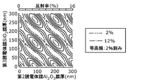
- FIG. 6A is a graph showing the reflectance with respect to the film thickness before aging of the dielectric multilayer film included in the nitride semiconductor laser device according to the embodiment.
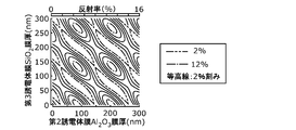
- FIG. 6B is a graph showing the reflectance with respect to the film thickness after aging of the dielectric multilayer film included in the nitride semiconductor laser device according to the embodiment.
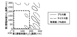
- FIG. 6C is a graph showing the amount of change in reflectance with respect to the film thickness before and after aging of the dielectric multilayer film included in the nitride semiconductor laser device according to the embodiment.
- FIG. 7 is a diagram for explaining the relationship between the film thickness of the second dielectric film and the third dielectric film and the reflectance of the dielectric multilayer film.
- FIG. 8A is a graph showing the reflectance with respect to the film thickness before aging of the dielectric multilayer film included in the nitride semiconductor laser device according to the embodiment.
- FIG. 8B is a graph showing the reflectance with respect to the film thickness before aging of the dielectric multilayer film included in the nitride semiconductor laser device according to the embodiment.
- FIG. 8C is a graph showing the reflectance with respect to the film thickness before aging of the dielectric multilayer film included in the nitride semiconductor laser device according to the embodiment.
- FIG. 8D is a graph showing the reflectance with respect to the film thickness before aging of the dielectric multilayer film included in the nitride semiconductor laser device according to the embodiment.
- FIG. 8A is a graph showing the reflectance with respect to the film thickness before aging of the dielectric multilayer film included in the nitride semiconductor laser device according to the embodiment.
- FIG. 8B is a graph showing the reflectance with respect to the film thickness before aging of the di
- FIG. 8E is a graph showing the reflectance with respect to the film thickness before aging of the dielectric multilayer film included in the nitride semiconductor laser device according to the embodiment.
- FIG. 8F is a graph showing the reflectance with respect to the film thickness before aging of the dielectric multilayer film included in the nitride semiconductor laser device according to the embodiment.
- FIG. 9A is a graph showing the amount of change in reflectance with respect to the film thickness before and after aging of the dielectric multilayer film included in the nitride semiconductor laser device according to the embodiment.
- FIG. 9B is a graph showing the amount of change in reflectance with respect to the film thickness before and after aging of the dielectric multilayer film included in the nitride semiconductor laser device according to the embodiment.
- FIG. 9A is a graph showing the amount of change in reflectance with respect to the film thickness before and after aging of the dielectric multilayer film included in the nitride semiconductor laser device according to the embodiment.
- FIG. 9B is
- FIG. 9C is a graph showing the amount of change in reflectance with respect to the film thickness before and after aging of the dielectric multilayer film included in the nitride semiconductor laser device according to the embodiment.
- FIG. 9D is a graph showing the amount of change in reflectance with respect to the film thickness before and after aging of the dielectric multilayer film included in the nitride semiconductor laser device according to the embodiment.
- FIG. 9E is a graph showing the amount of change in reflectance with respect to the film thickness before and after aging of the dielectric multilayer film included in the nitride semiconductor laser device according to the embodiment.
- FIG. 9C is a graph showing the amount of change in reflectance with respect to the film thickness before and after aging of the dielectric multilayer film included in the nitride semiconductor laser device according to the embodiment.
- FIG. 9D is a graph showing the amount of change in reflectance with respect to the film thickness before and after aging of the dielectric multilayer film included in the nitride semiconductor laser device according
- FIG. 9F is a graph showing the amount of change in reflectance with respect to the film thickness before and after aging of the dielectric multilayer film included in the nitride semiconductor laser device according to the embodiment.
- FIG. 10 is a diagram for explaining the relationship between the film thickness of the dielectric multilayer film and the film thickness variation of the dielectric multilayer film according to the embodiment.
- FIG. 11A is a graph showing the amount of change in reflectance with respect to the film thickness before and after aging of the dielectric multilayer film included in the nitride semiconductor laser device according to the embodiment.
- FIG. 11B is a graph showing the amount of change in reflectance with respect to the film thickness before and after aging of the dielectric multilayer film included in the nitride semiconductor laser device according to the embodiment.
- FIG. 11C is a graph showing the amount of change in reflectance with respect to the film thickness before and after aging of the dielectric multilayer film included in the nitride semiconductor laser device according to the embodiment.
- FIG. 11D is a graph showing the amount of change in reflectance with respect to the film thickness before and after aging of the dielectric multilayer film included in the nitride semiconductor laser device according to the embodiment.
- FIG. 11E is a graph showing the amount of change in reflectance with respect to the film thickness before and after aging of the dielectric multilayer film included in the nitride semiconductor laser device according to the embodiment.
- FIG. 11C is a graph showing the amount of change in reflectance with respect to the film thickness before and after aging of the dielectric multilayer film included in the nitride semiconductor laser device according to the embodiment.
- FIG. 11D is a graph showing the amount of change in reflectance with respect to the film thickness before and after aging of the dielectric multilayer film included in the nitride semiconductor laser device according
- FIG. 11F is a graph showing the amount of change in reflectance with respect to the film thickness before and after aging of the dielectric multilayer film included in the nitride semiconductor laser device according to the embodiment.
- FIG. 12 is a graph showing the reflectance of the dielectric multilayer film with respect to the wavelength of the nitride semiconductor laser device according to the embodiment.
- each figure is a schematic diagram and is not necessarily exactly illustrated. Therefore, the scales and the like do not always match in each figure.
- substantially the same configuration is designated by the same reference numerals, and duplicate description will be omitted or simplified.
- the terms “upper” and “lower” do not refer to the upward direction (vertically upward) and the downward direction (vertically downward) in absolute spatial recognition, but are based on the stacking order in the stacking configuration. It is used as a term defined by the relative positional relationship with. Also, the terms “upper” and “lower” are used not only when the two components are spaced apart from each other and another component exists between the two components, but also when the two components It also applies when they are placed in contact with each other.
- the X-axis, the Y-axis, and the Z-axis indicate the three axes of the three-dimensional Cartesian coordinate system.
- the Z-axis direction is the vertical direction
- the direction perpendicular to the Z-axis is the horizontal direction.
- the positive direction of the Z axis is vertically above.
- FIG. 1 is a schematic cross-sectional view showing the configuration of the nitride semiconductor laser device 10 according to the embodiment.
- FIG. 2 is a cross-sectional view schematically showing an example of deformation of the dielectric film when the nitride semiconductor laser device 10 according to the embodiment emits the laser beam 201.
- 1 and 2 are cross-sectional views taken along the line II of FIG. 4, which will be described later.
- the nitride semiconductor laser device 10 is formed by laser light sandwiched between the first conductive semiconductor layer 100a, the second conductive semiconductor layer 100b, the first conductive semiconductor layer 100a, and the second conductive semiconductor layer 100b.
- a laminated structure 100 having an active layer 103 that emits 201 is provided.
- a dielectric multilayer film 150 is formed on the front end surface 100F of the nitride semiconductor laser device 10 in order to resonate the laser beam 201 inside the laminated structure 100 and effectively emit the laser light 201 from the front end surface 100F.
- the dielectric multilayer film 150 is composed of, for example, a first dielectric film 120, a second dielectric film 130, and a third dielectric film 140. Specifically, the first dielectric film 120, the second dielectric film 130, and the third dielectric film 140 are arranged in this order on the front end surface 100F of the laminated structure 100.
- the first dielectric film 120 is a film that protects the front end surface 100F, and suppresses oxidation of the front end surface 100F due to diffusion of oxygen from the outside.
- the second dielectric film 130 and the third dielectric film 140 are films for adjusting the reflectance, respectively.
- the film thickness of the first dielectric film 120, the second dielectric film 130, and the third dielectric film 140 is formed substantially uniformly on the front end surface 100F.
- the film thickness and material of the dielectric multilayer film 150 were designed so as to be extremely small.
- the second dielectric film 130 and the third dielectric film 140 may be deformed by absorbing the laser beam 201 emitted from the laminated structure 100.
- the film thicknesses of the second dielectric film 130 and the third dielectric film 140 are set to the film thickness 300 of the portion through which the laser light 201 passes. It differs from the film thickness 301 of the portion through which the laser beam 201 does not pass. That is, the film thicknesses 300 and 301 of the second dielectric film 130 and the third dielectric film 140 are changed by emitting the laser beam 201 from the laminated structure 100, respectively.
- FIG. 3 is a graph showing the reflectance of the dielectric multilayer film with respect to the wavelength of the nitride semiconductor laser device according to the comparative example.
- the nitride semiconductor laser device according to the comparative example is the same as the nitride semiconductor laser device 10 according to the embodiment except for the material, film thickness, and refractive index used for the dielectric multilayer film.
- the reflectance before aging shown in FIG. 3 is the reflectance of light in a state of not being deformed by the laser beam 201, such as the dielectric multilayer film 150 shown in FIG. 1.
- the reflectance after aging shown in FIG. 3 is the reflectance of light in a state of being deformed by the laser beam 201, such as the dielectric multilayer film 150 shown in FIG.
- the position of the peak whose wavelength is around 400 nm differs between the reflectance before aging and the reflectance after aging.
- the reflectance of the dielectric multilayer film according to the comparative example the reflectance of the peak having a wavelength near 400 nm increases by about 1.5% by absorbing the laser beam. Therefore, the nitride semiconductor laser device according to the comparative example has different optical characteristics (specifically, optical output) before and after aging. Therefore, for example, if the nitride semiconductor laser device 10 is continuously used, the optical characteristics change with the passage of time.
- the inventors of the present application can suppress changes in optical characteristics by appropriately setting the material, film thickness, refractive index, etc. of the dielectric multilayer film 150 included in the nitride semiconductor laser device 10. I found. Specifically, the inventors of the present application have found that there are a film whose film thickness increases and a film whose film thickness decreases during aging. Therefore, the inventors of the present application have found that by appropriately combining a film whose film thickness increases during aging and a film whose film thickness decreases during aging, the change in reflectance can be suppressed even if the film thickness changes during aging.
- emitting the laser beam 201 from the laminated structure 100 is also simply referred to as aging.
- composition The configuration of the nitride semiconductor laser device 10 will be described with reference to FIGS. 1 and 4.
- FIG. 4 is a cross-sectional view showing the nitride semiconductor laser device 10 according to the embodiment in the IV-IV line of FIG.
- the nitride semiconductor laser device 10 is a nitride semiconductor light emitting device that emits laser light 201.
- the nitride semiconductor laser device 10 includes a laminated structure 100 and a dielectric multilayer film 150.
- the laminated structure 100 is a laminated body composed of a plurality of semiconductor layers including a waveguide 110. Further, the laminated structure 100 has a front side end surface 100F, which is a pair of resonator end faces facing each other, and a rear side end surface 100R.
- the dielectric multilayer film 150 is arranged on at least one of the pair of resonator end faces. In the present embodiment, the dielectric multilayer film 150 is arranged on the front end surface 100F.
- the laminated structure 100 includes a substrate 101, a first semiconductor layer 102, an active layer 103, a second semiconductor layer 104, a contact layer 105, an insulating layer 106, a second electrode 107, and a pad electrode 108. It has a first electrode 109 and.
- the first conductive semiconductor layer 100a in FIG. 1 includes a substrate 101 and a first semiconductor layer 102
- the second conductive semiconductor layer 100b includes a second semiconductor layer 104 and a contact layer 105.
- the insulating layer 106, the second electrode 107, the pad electrode 108, and the first electrode 109 are not shown.
- the laminated structure 100 is formed of a gallium nitride based material, which is an example of a nitride material.
- the light output has a wavelength in the band of about 390 nm or more and 420 nm or less. It is possible to realize a nitride semiconductor laser device 10 having optical characteristics of emitting a laser beam 201 of about 3 W or more and 10 W or less.
- the nitride semiconductor laser device 10 emits a laser beam 201 of 1 W or more.
- the oscillation wavelength of the nitride semiconductor laser device 10 is 420 nm or less. More specifically, the laminated structure 100 emits laser light 201 having a peak wavelength of 400 nm.
- the optical density of the laser beam 201 is 0.1 W / ⁇ m or more.
- the optical density is the light output / stripe width of the laser beam 201.
- the stripe width here is, for example, the width of the ridge portion described later (in the present embodiment, the length in the X-axis direction).
- the width of the ridge portion (hereinafter, also referred to as stripe width) is, for example, about 30 ⁇ m or more and 100 ⁇ m or less.
- the resonator length of the laminated structure 100 (in the present embodiment, the length in the Y-axis direction) is, for example, 1200 ⁇ m or more and 5000 ⁇ m or less.
- the optical characteristics of the nitride semiconductor laser device 10 are not limited to the above.
- the nitride semiconductor laser element 10 has a wavelength in the band of 365 nm or more and 390 nm or less by setting the input current to the laminated structure 100 to 2 A or more and 10 A or less and the input voltage to 3.5 V or more and 6 V or less.
- it may have an optical characteristic of emitting a laser beam 201 having an optical output of about 1 W or more and 5 W or less.
- the stripe width is about 8 ⁇ m or more and 100 ⁇ m or less.
- the resonator length of the laminated structure 100 is, for example, 800 ⁇ m or more and 5000 ⁇ m or less.
- the substrate 101 is a plate-shaped member that serves as a base material for the laminated structure 100.
- the substrate 101 is a GaN single crystal substrate having a thickness of 100 ⁇ m.
- the thickness of the substrate 101 is not limited to 100 ⁇ m, and may be, for example, 50 ⁇ m or more and 120 ⁇ m or less.
- the material forming the substrate 101 is not limited to the GaN single crystal, and may be sapphire, SiC, or the like.
- the first semiconductor layer 102 is a first conductive type semiconductor layer arranged above the substrate 101.
- the first semiconductor layer 102 is an n-type semiconductor layer arranged on one main surface of the substrate 101, and includes an n-type clad layer.
- the n-type clad layer is a layer made of n-AlGaN. The configuration of the n-type clad layer is not limited to this.
- the active layer 103 is a light emitting layer arranged above the first semiconductor layer 102.
- the active layer 103 is a quantum well active layer in which well layers made of InGaN and barrier layers made of GaN are alternately laminated, and has two well layers.
- the nitride semiconductor laser device 10 can emit blue laser light having a wavelength of about 400 nm.
- the configuration of the active layer 103 is not limited to this, and any quantum well active layer in which well layers and barrier layers are alternately laminated may be used.
- the active layer 103 may include a guide layer formed on at least one of the upper side and the lower side of the quantum well active layer.
- the second semiconductor layer 104 is a second conductive type semiconductor layer arranged above the active layer 103.
- the second conductive type is a conductive type different from the first conductive type.
- the second semiconductor layer 104 is a p-type semiconductor layer and includes a p-type clad layer.
- the p-type clad layer is a superlattice layer in which 100 layers of p-AlGaN and 100 layers of GaN having a thickness of 3 nm are alternately laminated.
- the structure of the p-type clad layer is not limited to this.
- the first semiconductor layer 102, the active layer 103, and the second semiconductor layer 104 form a waveguide 110 which is a waveguide of the laser beam 201.
- the waveguide 110 is a portion where the laser beam 201 is guided inside the laminated structure 100.
- the waveguide 110 is composed of, for example, a part of the first semiconductor layer 102, a part of the active layer 103, and a part of the second semiconductor layer 104.
- the contact layer 105 is a second conductive type semiconductor layer that makes ohmic contact with the second electrode 107.
- the contact layer 105 is a p-type semiconductor layer and is a layer made of p-GaN.
- the configuration of the contact layer 105 is not limited to this.
- a ridge portion is formed on the second semiconductor layer 104 and the contact layer 105.
- the region of the active layer 103 corresponding to the ridge portion serves as a light emitting point and emits the laser beam 201.
- the first electrode 109 is an electrode arranged on the lower main surface of the substrate 101 (that is, the main surface on which the first semiconductor layer 102 or the like is not arranged).
- the first electrode 109 is, for example, a laminated film in which Ti, Pt, and Au are laminated in order from the substrate 101 side.
- the configuration of the first electrode 109 is not limited to this.
- the second electrode 107 is an electrode arranged on the contact layer 105.
- the second electrode 107 is a p-side electrode that makes ohmic contact with the contact layer 105.
- a pad electrode 108 is arranged on the p-side electrode.
- the second electrode 107 is, for example, a laminated film in which Pd and Pt are laminated in order from the contact layer 105 side.
- the configuration of the second electrode 107 is not limited to this.
- the pad electrode 108 is a pad-shaped electrode arranged above the second electrode 107.
- the pad electrode 108 is, for example, a laminated film in which Ti and Au are laminated in order from the second electrode 107 side, and is arranged in and around the ridge portion.
- the configuration of the pad electrode 108 is not limited to this.
- the laminated structure 100 may further have an insulating film such as a SiO 2 film covering the side wall of the ridge portion or the like in addition to the above layers.
- an insulating film such as a SiO 2 film covering the side wall of the ridge portion or the like in addition to the above layers.
- the laminated structure 100 is a so-called single emitter having one ridge portion (emitter), but has a plurality of (for example, about 60) ridge portions, so-called multi-emitter. It may be.
- the total light output of the laser beam 201 emitted from below each of the plurality of ridge portions in the laminated structure 100 is about 100 W or more and 200 W or less.
- the dielectric multilayer film 150 is a protective film arranged on the front end surface 100F of the laminated structure 100. Specifically, the dielectric multilayer film 150 protects the front side end surface 100F of the laminated structure 100 and reduces the reflectance of the laser beam 201 on the front side end surface 100F.
- the first dielectric film 120, the second dielectric film 130, and the third dielectric film 140 are arranged in this order from the resonator end face (front side end face 100F in the present embodiment) side. Have.
- the first dielectric film 120 is a dielectric layer arranged on the frontmost end surface 100F side of the first dielectric film 120, the second dielectric film 130, and the third dielectric film 140.
- the first dielectric film 120 may include at least one layer of a dielectric film composed of at least one of a nitride film and an acid nitride film.
- the first dielectric film 120 is directly connected to the front end surface 100F of the laminated structure 100. That is, the first dielectric film 120 is formed in contact with the front end surface 100F. Therefore, by using a nitrided film or an acid nitrided film having the same crystallinity as the laminated structure 100 as the first dielectric film 120, the protection performance of the front end surface 100F can be enhanced.
- the first dielectric film 120 is composed of n (n is a positive integer) layer protective film from the first protective film to the nth protective film in order from the front side end surface 100F side.
- the first protective film 121 is a dielectric film arranged on the most front side end surface 100F side among the plurality of protective films of the first dielectric film 120.
- the first protective film 121 is a film containing a SiN film. More specifically, the first protective film 121 is a film made of a SiN film having a thickness d1 of about 0.5 nm.
- the configuration of the first protective film 121 is not limited to this.
- the first protective film 121 may be, for example, another oxynitride film such as SiON.
- the second protective film 122 is a dielectric film laminated on the first protective film 121.
- the second protective film 122 is a film containing an AlON film. More specifically, the second protective film 122 is a film made of an AlON film having a thickness d2 of about 21 nm.
- the configuration of the second protective film 122 is not limited to this.
- the second protective film 122 may be, for example, another oxynitride film such as SiON, or a nitride film such as an AlN film or SiN film.
- the third protective film 123 is a dielectric film laminated on the second protective film 122.
- the third protective film 123 is a film made of an Al 2 O 3 film having a thickness d3 of about 13 nm.
- the configuration of the third protective film 123 is not limited to this.
- the third protective film 123 may be, for example, another dielectric film such as SiO 2.
- the fourth protective film 124 is a dielectric film laminated on the third protective film 123.
- the fourth protective film 124 may include a dielectric film composed of at least one of a nitride film and an acid nitride film.
- the fourth protective film 124 is a film made of an AlON film having a thickness d4 of about 11 nm.
- the configuration of the fourth protective film 124 is not limited to this.
- the fourth protective film 124 may be, for example, another nitride film such as SiN, or an acid nitride film such as an AlN film or a SiON film.
- the second dielectric film 130 is a dielectric film laminated on the outside of the first dielectric film 120.
- the second dielectric film 130 is an Al 2 O 3 film having a thickness of about 167 nm.
- the third dielectric film 140 is a dielectric film laminated on the outside of the second dielectric film 130.
- the third dielectric film 140 is a SiO 2 film having a thickness of about 58 nm.
- FIG. 5 is a table showing changes in film thickness with respect to aging conditions.
- the peak wavelength (oscillation wavelength) of the laser beam 201 is 405 nm.
- condition 1 of FIG. 5 when the laser beam 201 of 4.5 W is emitted from the laminated structure 100 for 736 hours at 25 ° C., the thickness of the second dielectric film 130 made of the Al 2 O 3 film is increased. The rate of change was -8.5% at the maximum and -6.2% at the minimum due to variations in the light intensity distribution of the laser beam 201. Further, under condition 1, the rate of change in the film thickness of the third dielectric film 140 made of the SiO 2 film was + 5.3% at the maximum and 3.7% at the minimum.
- the optical density under condition 1 is 0.15 (W / ⁇ m).
- Condition 2 of FIG. 5 when the laser beam 201 of 1 W is emitted from the laminated structure 100 for 4500 h at 25 ° C., the film thickness of the second dielectric film 130 made of the Al 2 O 3 film is increased. The rate of change was -8.7% at the maximum and -7.0% at the minimum. Further, under condition 2, the rate of change in the film thickness of the third dielectric film 140 made of the SiO 2 film was + 5.2% at the maximum and 4.0% at the minimum.
- the optical density under condition 2 is 0.149 (W / ⁇ m).
- the rate of change in the film thickness of the second dielectric film 130 made of the Al 2 O 3 film was ⁇ 7.6% on average. Further, the rate of change in the film thickness of the third dielectric film 140 made of the SiO 2 film under the conditions 1 and 2 was + 4.6% on average.
- the rate of change in the film thickness of the second dielectric film 130 made of the Al 2 O 3 film decreases sharply when the optical density is about 0.15 W / ⁇ m and the aging time is 1000 h or less, and the aging time is 1000 h or later. Then, the change gradually decreased, though it became gradual. Further, the rate of change in the film thickness of the third dielectric film 140 made of the SiO 2 film increases sharply within 1000 hours when the optical density is about 0.15 W / ⁇ m, and changes after 1000 hours. Gradually increased, albeit slowly.
- the second dielectric film 130 made of the Al 2 O 3 film shrinks due to aging and the film thickness decreases.
- the film made of Al 2 O 3 film is amorphous containing several% of Ar in the state (as-depo.) Immediately after the film is formed. However, as-depo. It is considered that the film made of Al 2 O 3 film shrinks due to the desorption of Ar due to the optical load due to aging, and the film thickness decreases.
- the third dielectric film 140 made of the SiO 2 film expands due to aging and the film thickness increases.
- the third dielectric layer 140 made of SiO 2 film, Al 2 O 3 first 2 Ar contained in the dielectric film 130 made of film is desorbed, film by diffusing into the SiO 2 film is expanded It is considered that the film thickness has increased.
- the third dielectric film 140 has an amorphous structure. Further, for example, the third dielectric film 140 is any one of SiO 2 , B 2 O 3 , P 2 O 5 , and GeO 2.
- the second dielectric film 130 is one of Al 2 O 3 , Ta 2 O 5 , and ZrO 2 .
- one of the second dielectric film 130 and the third dielectric film 140 has a property that the film thickness is reduced by the laser light 201 emitted from the nitride semiconductor laser element 10.
- the film thickness is increased by the laser beam 201 emitted from the nitride semiconductor laser device 10.
- the second dielectric film 130 has a property that the film thickness is reduced by the laser light 201 emitted from the nitride semiconductor laser device 10.
- the third dielectric film 140 has a property that the film thickness is increased by the laser light 201 emitted from the nitride semiconductor laser device 10.
- the second dielectric film 130 has a recess 131.
- the convex portion 141 is formed on the third dielectric film 140. Further, for example, the change in the film thickness of the second dielectric film 130 and the third dielectric film 140 is caused by the optical path of the laser beam 201 emitted from the front end surface 100F (for example, on the optical axis 200 of the laser beam 201). appear.
- the dielectric multilayer film 150 has a film thickness and a refractive index as described later, so that the laser light 201 is about 10,000 hours. Even if the light is emitted, the reduction rate of the light output is 20% or less.
- a coat film 160 may be arranged between the front end surface 100F and the dielectric multilayer film 150.
- the coat film 160 is a film that protects the front end face 100F, and is, for example, an aluminum nitride film.
- the aluminum nitride film may contain crystalline aluminum nitride.
- the aluminum nitride film may be crystalline aluminum nitride.
- the material used for the coating film 160 is not limited to this.
- the materials used for the coat film 160 include aluminum nitride silicon, aluminum gallium nitride, aluminum nitride yttrium, aluminum lanthanum nitride, aluminum nitride silicon, aluminum gallium nitride, and aluminum nitride yttrium. It may be at least one with the aluminum nitride lantern. Further, the above-mentioned material may be used as the material of the first dielectric film 120.
- such a dielectric multilayer film 150 has a film thickness and a refractive index as described later, so that, for example, the reflectance with respect to light having a wavelength of 400 nm is about 4% or more and 20 or less. Further, by adopting the so-called AR (Anti Reflection) coating technology for the dielectric multilayer film 150, the dielectric multilayer film 150 may have a reflectance of 0.1% or less with respect to light having a wavelength of 400 nm.
- the dielectric multilayer film 150 may be provided on the rear end surface 100R.
- the inventors of the present application carried out an optical simulation of the dielectric multilayer film 150 in order to determine a condition in which the change in reflectance is small even if the film thickness changes.
- the second dielectric film 130 is an Al 2 O 3 film
- the third dielectric film 140 is a SiO 2 film.
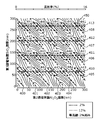
- FIG. 6A is a graph showing the reflectance with respect to the film thickness before aging of the dielectric multilayer film 150 included in the nitride semiconductor laser device 10 according to the embodiment.
- FIG. 6B is a graph showing the reflectance with respect to the film thickness after aging of the dielectric multilayer film 150 included in the nitride semiconductor laser device 10 according to the embodiment.
- FIG. 6C is a graph showing the amount of change in reflectance with respect to the film thickness before and after aging of the dielectric multilayer film 150 included in the nitride semiconductor laser device 10 according to the embodiment.
- FIGS. 6A to 6C conditions such as the film thickness and the refractive index of the first dielectric film 120 are fixed. Further, in FIGS. 6A to 6C, the second dielectric film 130 is an Al 2 O 3 film, and the third dielectric film 140 is a SiO 2 film. In FIGS. 6A to 6C, the film thickness of these films is changed in the range of 0 nm to 300 nm, the reflectance is calculated, and contour lines are displayed.
- the film thickness shown in FIG. 6B indicates the film thickness before aging. Specifically, the graph shown in FIG. 6B shows that the film thickness of the second dielectric film 130 is ⁇ 7.6% of the film thickness of the second dielectric film 130 and the third dielectric film 140 before aging. Then, the reflectance when the film thickness of the third dielectric film 140 is + 4.6% is calculated and displayed as contour lines.
- FIG. 6C shows the calculation result of the difference in reflectance before and after aging. Specifically, the graph shown in FIG. 6C shows a value obtained by subtracting the reflectance of the graph shown in FIG. 6B from the reflectance of the graph shown in FIG. 6A.
- contour lines are shown in increments of + 3% for the amount of change on the positive side of the reflectance from + 1.5%, and the amount of change on the negative side of the reflectance is -3% in order from -1.5%. Contour lines are shown in increments.
- FIG. 7 is a diagram for explaining the relationship between the film thickness of the second dielectric film 130 and the third dielectric film 140 and the reflectance of the dielectric multilayer film 150.
- the graph showing the reflectance with respect to the film thickness shown in FIG. 7 is the same as that in FIG. 6A.
- One or more protective films (four protective films in the present embodiment) in the first dielectric film 120 are applied in order from the front end surface 100F side to the first protective film, the second protective film, ...
- the n-layer film of the n-protective film is used, and the refractive index and the film thickness of the k-th protective film (k is a positive integer) are nk and dk, respectively, and the refractive index and the film thickness of the second dielectric film 130 are defined.
- Ni and di, respectively, the refractive index and the film thickness of the third dielectric film 140 are nj and dj, respectively, and the sum of the optical film thicknesses of one or more protective films in the first dielectric film 120 is A. Then, the following equation (1) is satisfied.
- broken lines 400 to 407 shown in FIG. 7 satisfy the following formula (2) in order from the left side of the paper.
- m1 is a positive integer.
- the reflectance of the dielectric multilayer film 150 takes a maximum value when m1 is an even number, and becomes a minimum value when m1 is an odd number.
- the change between the maximum and the minimum reflectance of the dielectric multilayer film 150 is a film having a relational expression between the optical film thickness and the reflectance of the SiO 2 film, which is the third dielectric film 140 derived from Fresnel's equation.
- the period coincides with cos (4 ⁇ ⁇ nj ⁇ dj / ⁇ ), which is a proportional term of thickness. That is, the multiplication (that is, the optical film thickness) between the film thickness of the third dielectric film 140 and the refractive index at which the reflectance of the dielectric multilayer film 150 is maximized or minimized satisfies the following equation (3).
- the optical refractive index and film thickness of the third dielectric film 140 are nj and dj, respectively.
- the relationship between the optical film thickness of the second dielectric film 130 and the reflectance is such that although the period between the maximum and the minimum is ⁇ / 4, the optical film thickness that becomes the maximum or the minimum is the first dielectric film. It is not necessarily an integral multiple of ⁇ / 4 because it is affected by the film thickness of 120.
- the film thickness and the refractive index of the second dielectric film 130 which maximizes or minimizes the reflectance of the dielectric multilayer film 150, satisfy the following formula (5).
- the refractive index and the film thickness of the second dielectric film 130 are ni and di, respectively.
- N2 is a positive integer.
- D becomes a broken line 420.
- B becomes a broken line 421.
- B becomes a broken line 422.
- 8A to 8F are graphs showing the reflectance with respect to the film thickness before aging of the dielectric multilayer film 150 included in the nitride semiconductor laser device 10 according to the embodiment.
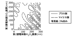
- 9A to 9F are graphs showing the amount of change in reflectance with respect to the film thickness before and after aging of the dielectric multilayer film 150 included in the nitride semiconductor laser device 10 according to the embodiment.
- FIGS. 8A and 9A are graphs when the optical film thickness of the first dielectric film 120 is ⁇ / 8.
- 8B and 9B are graphs when the optical film thickness of the first dielectric film 120 is 3 ⁇ ⁇ / 16.
- 8C and 9C are graphs when the optical film thickness of the first dielectric film 120 is ⁇ / 4.
- 8D and 9D are graphs when the optical film thickness of the first dielectric film 120 is 5 ⁇ ⁇ / 16.
- 8E and 9E are graphs when the optical film thickness of the first dielectric film 120 is 3 ⁇ ⁇ / 8.
- 8F and 9F are graphs when the optical film thickness of the first dielectric film 120 is ⁇ / 2.
- ⁇ indicates the oscillation wavelength of the laser beam 201, which is 400 nm in the present embodiment.
- contour lines are shown in increments of + 3% in order from + 1.5% for the amount of change on the positive side of the reflectance, and in order from -1.5% for the amount of change on the negative side of the reflectance. Contour lines are shown in -3% increments.
- the amount of change in reflectance is about ⁇ 1.5% or more and + 1.5% or less within the broken line 430.
- the broken line 430 indicates a range in which the film thickness of the second dielectric film 130 is 3 ⁇ ⁇ / 4 or less and the film thickness of the third dielectric film 140 is 3 ⁇ ⁇ / 4 or less.
- the optical film thickness of the first dielectric film 120 (more specifically, the total optical film thickness of the plurality of protective films of the first dielectric film 120) is 3 ⁇ ⁇ / 16 or more and 5 ⁇ .
- the first film thickness is ⁇ / 16 or less
- the optical film thickness of the second dielectric film 130 is 3 ⁇ ⁇ / 4 or less
- the optical film thickness of the third dielectric film 140 is 3 ⁇ ⁇ / 4 or less.
- a plurality of nitride semiconductor laser devices 10 in which the dielectric multilayer film 150 is formed on the laminated structure 100 are manufactured, a plurality of nitride semiconductor lasers are manufactured due to manufacturing variations even if the dielectric multilayer film 150 is manufactured with the same film thickness.
- the film thicknesses of the respective dielectric multilayer films 150 of the element 10 do not completely match.
- FIG. 10 is a diagram for explaining the relationship between the film thickness of the dielectric multilayer film 150 and the film thickness variation of the dielectric multilayer film 150.
- the graph showing the reflectance with respect to the film thickness shown in FIG. 10 is the same as that in FIG. 6A.
- the change in the reflectance with respect to the change in the film thickness of the dielectric multilayer film 150 is considered to be small, that is, stable.
- the maximum value, the minimum value, and the saddle point of the reflectance in the graph shown in FIG. 10 are the intersection points 440 to 443 between any of the broken lines 400 to 404 shown in FIG. 10 and any of the broken lines 410 to 413.
- the maximum value, the minimum value, and the saddle point of the reflectance in the graph shown in FIG. 10 are film thicknesses satisfying the above formula (1) and the above formula (3).
- the reflectance when A in the above equation (1) is an even number and B in the above equation (3) is an even number, the reflectance shows a maximum and becomes one of a plurality of intersections 440. Further, for example, when A in the above equation (1) is an even number and B in the above equation (3) is an odd number, the reflectance indicates a saddle point and is any of a plurality of intersection points 441. For example, when A in the above equation (1) is an odd number and B in the above equation (3) is an even number, the reflectance indicates a saddle point and is any of a plurality of intersections 442. For example, when A in the above equation (1) is an odd number and B in the above equation (3) is an even number, the reflectance indicates a minimum and becomes any of a plurality of intersections 443.
- the reflectance of the dielectric multilayer film 150 it is preferable to select the intersection points 440 or 443 in order to realize a high reflectance, and it is preferable to select the intersection points 441 or 442 in order to realize a low reflectance. ..
- the change in reflectance can be reduced with respect to the change in the film thickness of the dielectric multilayer film 150.
- the change in reflectance can be reduced with respect to the change in the film thickness of the dielectric multilayer film 150.
- the region surrounded by the broken line 450 satisfies the following equations (7) and (8).
- n1 and m2 are both positive integers.
- the change in reflectance can be reduced with respect to the change in the film thickness of the dielectric multilayer film 150.
- m1 an integer of 2 or more
- the change in reflectance can be further reduced with respect to the change in the film thickness of the dielectric multilayer film 150.
- m2 1, in other words, by using the following equation (9), the change in reflectance can be further reduced with respect to the change in the film thickness of the dielectric multilayer film 150.
- m3 is a positive integer.
- the change (change) in the reflectance of the dielectric multilayer film 150 is suppressed. can. Therefore, fluctuations in the light output during driving of the nitride semiconductor laser device 10 and deterioration of the nitride semiconductor laser device 10 can be suppressed.
- the amount of change in the reflectance of the dielectric multilayer film 150 can be reduced even when aging is performed, and the amount of change in the reflectance of the dielectric multilayer film 150 can be reduced.
- the change in reflectance can be reduced with respect to the change in the film thickness of the dielectric multilayer film 150. That is, according to the nitride semiconductor laser device 10 including the dielectric multilayer film 150 that satisfies the above-mentioned first film thickness condition and the above-mentioned second film thickness condition, the change in optical characteristics can be suppressed.
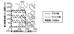
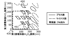
- FIGS. 11A to 11F are graphs showing the amount of change in reflectance with respect to the film thickness before and after aging of the dielectric multilayer film 150 included in the nitride semiconductor laser device 10 according to the embodiment.
- the graphs showing the reflectance with respect to the film thickness shown in FIGS. 11A to 11F are the same as those in FIGS. 9A to 9F.
- the change in reflectance can be reduced with respect to the change in the film thickness of the dielectric multilayer film 150.
- the amount of change in the reflectance of the dielectric multilayer film 150 can be reduced even when aging is performed. That is, if it is within the range of the region surrounded by the broken line 430 and within the range of the region surrounded by the broken line 450 shown in FIGS. 11B to 11D, the change in the optical characteristics of the dielectric multilayer film 150 is changed. It can be suppressed more.
- FIG. 12 is a graph showing the reflectance of the dielectric multilayer film 150 with respect to the wavelength of the nitride semiconductor laser device 10 according to the embodiment.
- the graph shown in FIG. 12 is within the condition of the film thickness of the dielectric multilayer film 150 at the position 461 shown in FIG. 11C, that is, within the range of the region surrounded by the broken line 430 and surrounded by the broken line 450.
- the reflectance of the dielectric multilayer film 150 that satisfies the condition of the film thickness within the range of the region is shown.
- the graph shown in FIG. 3 is outside the range of the film thickness condition of the dielectric multilayer film 150 at the position 460 shown in FIG. 11B, that is, the region surrounded by the broken line 430, and is surrounded by the broken line 450.
- the reflectance of the dielectric multilayer film satisfying the condition of the film thickness outside the range of the region is shown.
- the reflectance of the dielectric multilayer film 150 satisfying the above-mentioned first film thickness condition and the above-mentioned second film thickness condition is almost the same before and after aging with respect to light having a wavelength of, for example, 400 nm. It can be seen that there is no change.
- the nitride semiconductor laser device 10 is composed of a plurality of semiconductor layers (for example, the first semiconductor layer 102, the active layer 103, and the second semiconductor layer 104) including the waveguide 110 and faces each other.
- the body multilayer film 150 is provided.
- the dielectric multilayer film 150 has a first dielectric film 120, a second dielectric film 130, and a third dielectric film 140 in this order from the resonator end face side.
- the first dielectric film 120 is composed of n (n is a positive integer) layer protective film from the first protective film to the nth protective film in order from the resonator end face side.
- the refractive index and the film thickness of the k (k is an integer satisfying 1 ⁇ k ⁇ n) th protective film in the first dielectric film 120 are nk and dk, respectively, and the second dielectric is used.
- the refractive index and film thickness of the body film 130 are ni and di, respectively, the refractive index and film thickness of the third dielectric film 140 are nj and dj, respectively, m1 is an integer of 2 or more, and m2 is positive.
- the film thickness and the refractive index of each film included in the dielectric multilayer film 150 are appropriately combined to form the film of the dielectric multilayer film 150. Even if the thickness fluctuates, the fluctuation of the reflectance can be suppressed to a small extent. Therefore, fluctuations in the light output during driving of the nitride semiconductor laser device 10 and deterioration of the nitride semiconductor laser device 10 can be suppressed. That is, according to the nitride semiconductor laser device 10, deterioration of optical characteristics can be suppressed.
- the nitride semiconductor laser device 10 satisfies the above formula (7) and also satisfies the above formula (8).
- one of the second dielectric film 130 and the third dielectric film 140 has a property that the film thickness is reduced by the laser light 201 emitted from the nitride semiconductor laser device 10, and the other is a nitride semiconductor laser. It has a property that the film thickness is increased by the laser light 201 emitted from the element 10.
- the film thickness and the refractive index of each film included in the dielectric multilayer film 150 are appropriately combined to form the film of the dielectric multilayer film 150. Even if the thickness fluctuates, the fluctuation of the reflectance can be suppressed to a small extent. Therefore, fluctuations in the light output during driving of the nitride semiconductor laser device 10 and deterioration of the nitride semiconductor laser device 10 can be suppressed.
- a recess 131 is formed in the second dielectric film 130 at the interface between the second dielectric film 130 and the third dielectric film 140 in response to the laser light 201 emitted from the end face of the resonator.
- the convex portion 141 is formed on the third dielectric film 140.
- the amount of change in the total film thickness of the dielectric multilayer film 150 can be reduced even when the laser beam 201 is irradiated. Therefore, the change in the reflectance of the dielectric multilayer film 150 is further suppressed.
- the change in the film thickness of the second dielectric film 130 and the third dielectric film 140 occurs in the optical path of the laser beam 201 emitted from the end face of the resonator.
- the change in the film thickness of the dielectric multilayer film 150 occurs on the optical path of the laser light 201, the amount of change in the total film thickness of the dielectric multilayer film 150 in the region through which the laser light 201 passes is reduced. .. Therefore, the change in the reflectance of the dielectric multilayer film 150 is further suppressed.
- the third dielectric film 140 has an amorphous structure.
- a third dielectric film 140 having a property of taking in a rare gas such as Ar contained in the second dielectric film 130 to increase the film thickness is realized.
- the nitride semiconductor laser device 10 further satisfies the above equation (9).
- the amount of change in the total film thickness of the dielectric multilayer film 150 can be reduced even when the laser beam 201 is irradiated. Therefore, the change in the reflectance of the dielectric multilayer film 150 is further suppressed.
- the oscillation wavelength of the nitride semiconductor laser device 10 is 420 nm or less.
- the configuration of the dielectric multilayer film 150 is as an end face coating film in the nitride semiconductor laser device 10 that emits a laser beam 201 having a wavelength of 420 nm or less, which is a wavelength at which the dielectric multilayer film 150 easily absorbs the laser beam 201. , Especially effective.
- the nitride semiconductor laser element 10 emits a laser beam 201 of 1 W or more.
- the change in the film thickness of the dielectric multilayer film 150 largely depends on the light output of the laser beam 201.
- the change in the film thickness of the dielectric multilayer film 150 is remarkably observed in the laser light 201 having an optical output of 1 W or more. Therefore, the configuration of the dielectric multilayer film 150 is particularly effective as an end face coating film in the nitride semiconductor laser device 10 that emits a laser beam 201 of 1 W or more that easily affects the film thickness of the dielectric multilayer film 150. ..
- the nitride semiconductor laser device 10 satisfies the above equation (10) when m3 is a positive integer.
- the amount of change in the total film thickness of the dielectric multilayer film 150 can be reduced even when the laser beam 201 is irradiated. Therefore, the change in the reflectance of the dielectric multilayer film 150 is further suppressed.
- the second dielectric film 130 is either Al 2 O 3 , Ta 2 O 5 , or ZrO 2
- the third dielectric film 140 is SiO 2 , B 2 O 3 , P 2. It is either O 5 or GeO 2.
- the dielectric multilayer film 150 a film whose film thickness decreases and a film whose film thickness increases by absorbing the laser beam 201 can be combined. Therefore, fluctuations in the light output during driving of the nitride semiconductor laser device 10 and deterioration of the nitride semiconductor laser device 10 can be suppressed.
- an aluminum nitride film is arranged between the resonator end face and the dielectric multilayer film 150.
- the aluminum nitride film can suppress the oxidation of the resonator end face in the nitride semiconductor laser device 10. Further, according to this, the dangling bond in the resonator end face and the dielectric multilayer film 150 can be reduced. Therefore, for example, even when the nitride semiconductor laser device 10 is driven so as to have a high light output, the deterioration of the dielectric multilayer film 150 can be suppressed.
- the aluminum nitride film contains crystalline aluminum nitride.
- the aluminum oxynitride film may be polycrystalline aluminum nitride, or may be a film containing a large amount of oxygen at the grain boundaries of the polycrystalline aluminum nitride.
- the oxidation of the resonator end face in the nitride semiconductor laser device 10 can be further suppressed by the inclusion of crystals in the aluminum nitride film. Further, according to this, the dangling bond in the resonator end face and the dielectric multilayer film 150 can be further reduced. Therefore, for example, even when the nitride semiconductor laser device 10 is driven so as to have a high light output, the deterioration of the dielectric multilayer film 150 can be further suppressed.
- a film composed of at least one of aluminum nitride yttrium and aluminum nitride lantern is arranged.
- This also makes it possible to suppress the oxidation of the resonator end face in the nitride semiconductor laser device 10 as in the case of the aluminum nitride film. Further, according to this, the dangling bond in the resonator end face and the dielectric multilayer film 150 can be reduced. Therefore, for example, even when the nitride semiconductor laser device 10 is driven so as to have a high light output, the deterioration of the dielectric multilayer film 150 can be suppressed.
- the nitride semiconductor laser device of the present disclosure is used, for example, as a light source for industrial lighting, facility lighting, industrial laser equipment such as in-vehicle head lamps and laser processing machines, and image display devices such as laser displays and projectors. can do.
- Dielectric semiconductor laser element 100 Laminated structure 100a First conductive semiconductor layer 100b Second conductive semiconductor layer 100F Front side end face 100R Rear side end face 101 Substrate 102 First semiconductor layer 103 Active layer 104 Second semiconductor layer 105 Contact layer 106 Insulation layer 107 2nd electrode 108 Pad electrode 109 1st electrode 110 waveguide 120 1st dielectric film 121 1st protective film 122 2nd protective film 123 3rd protective film 124 4th protective film 130 2nd dielectric film 131 Concave 140 Third dielectric film 141 Convex 150 Dielectric multilayer film 160 Coat film 200 Optical axis 201 Laser light 300, 301, d1, d2, d3, d4, di, dj Film thickness 400-408, 410-413, 420 ⁇ 423, 430, 450 Broken line 440 ⁇ 443 Intersection 460, 461 Position
Landscapes
- Physics & Mathematics (AREA)
- Condensed Matter Physics & Semiconductors (AREA)
- General Physics & Mathematics (AREA)
- Electromagnetism (AREA)
- Optics & Photonics (AREA)
- Semiconductor Lasers (AREA)
Priority Applications (3)
| Application Number | Priority Date | Filing Date | Title |
|---|---|---|---|
| JP2022511951A JP7708740B2 (ja) | 2020-03-30 | 2021-03-22 | 窒化物半導体レーザ素子 |
| US17/951,000 US20230019645A1 (en) | 2020-03-30 | 2022-09-22 | Nitride semiconductor laser element |
| JP2025112751A JP2025129325A (ja) | 2020-03-30 | 2025-07-03 | 窒化物半導体レーザ素子 |
Applications Claiming Priority (2)
| Application Number | Priority Date | Filing Date | Title |
|---|---|---|---|
| JP2020-060225 | 2020-03-30 | ||
| JP2020060225 | 2020-03-30 |
Related Child Applications (1)
| Application Number | Title | Priority Date | Filing Date |
|---|---|---|---|
| US17/951,000 Continuation US20230019645A1 (en) | 2020-03-30 | 2022-09-22 | Nitride semiconductor laser element |
Publications (1)
| Publication Number | Publication Date |
|---|---|
| WO2021200328A1 true WO2021200328A1 (ja) | 2021-10-07 |
Family
ID=77928125
Family Applications (1)
| Application Number | Title | Priority Date | Filing Date |
|---|---|---|---|
| PCT/JP2021/011639 Ceased WO2021200328A1 (ja) | 2020-03-30 | 2021-03-22 | 窒化物半導体レーザ素子 |
Country Status (3)
| Country | Link |
|---|---|
| US (1) | US20230019645A1 (https=) |
| JP (2) | JP7708740B2 (https=) |
| WO (1) | WO2021200328A1 (https=) |
Cited By (1)
| Publication number | Priority date | Publication date | Assignee | Title |
|---|---|---|---|---|
| WO2024004677A1 (ja) * | 2022-06-28 | 2024-01-04 | パナソニックホールディングス株式会社 | 半導体レーザ素子 |
Citations (10)
| Publication number | Priority date | Publication date | Assignee | Title |
|---|---|---|---|---|
| JP2008218523A (ja) * | 2007-02-28 | 2008-09-18 | Nichia Chem Ind Ltd | 窒化物半導体レーザ素子及びその製造方法 |
| JP2008244454A (ja) * | 2007-02-26 | 2008-10-09 | Toshiba Corp | 半導体レーザ装置 |
| WO2009147853A1 (ja) * | 2008-06-06 | 2009-12-10 | パナソニック株式会社 | 半導体発光素子 |
| JP2010153810A (ja) * | 2008-11-21 | 2010-07-08 | Sanyo Electric Co Ltd | 窒化物系半導体レーザ素子および光ピックアップ装置 |
| JP2011009374A (ja) * | 2009-06-24 | 2011-01-13 | Panasonic Corp | 窒化物半導体レーザ |
| JP2012109499A (ja) * | 2010-11-19 | 2012-06-07 | Sony Corp | 半導体レーザ素子およびその製造方法 |
| US20130343419A1 (en) * | 2012-04-04 | 2013-12-26 | Osram Opto Semiconductors Gmbh | Laser Diode Assembly |
| WO2014002339A1 (ja) * | 2012-06-29 | 2014-01-03 | パナソニック株式会社 | 窒化物半導体発光素子 |
| WO2014097508A1 (ja) * | 2012-12-19 | 2014-06-26 | パナソニック株式会社 | 窒化物半導体レーザ素子 |
| WO2019159449A1 (ja) * | 2018-02-14 | 2019-08-22 | パナソニックIpマネジメント株式会社 | 窒化物半導体レーザ素子及び照明光源モジュール |
Family Cites Families (1)
| Publication number | Priority date | Publication date | Assignee | Title |
|---|---|---|---|---|
| US7668218B2 (en) * | 2007-02-20 | 2010-02-23 | Nichia Corporation | Nitride semiconductor laser element |
-
2021
- 2021-03-22 JP JP2022511951A patent/JP7708740B2/ja active Active
- 2021-03-22 WO PCT/JP2021/011639 patent/WO2021200328A1/ja not_active Ceased
-
2022
- 2022-09-22 US US17/951,000 patent/US20230019645A1/en active Pending
-
2025
- 2025-07-03 JP JP2025112751A patent/JP2025129325A/ja active Pending
Patent Citations (10)
| Publication number | Priority date | Publication date | Assignee | Title |
|---|---|---|---|---|
| JP2008244454A (ja) * | 2007-02-26 | 2008-10-09 | Toshiba Corp | 半導体レーザ装置 |
| JP2008218523A (ja) * | 2007-02-28 | 2008-09-18 | Nichia Chem Ind Ltd | 窒化物半導体レーザ素子及びその製造方法 |
| WO2009147853A1 (ja) * | 2008-06-06 | 2009-12-10 | パナソニック株式会社 | 半導体発光素子 |
| JP2010153810A (ja) * | 2008-11-21 | 2010-07-08 | Sanyo Electric Co Ltd | 窒化物系半導体レーザ素子および光ピックアップ装置 |
| JP2011009374A (ja) * | 2009-06-24 | 2011-01-13 | Panasonic Corp | 窒化物半導体レーザ |
| JP2012109499A (ja) * | 2010-11-19 | 2012-06-07 | Sony Corp | 半導体レーザ素子およびその製造方法 |
| US20130343419A1 (en) * | 2012-04-04 | 2013-12-26 | Osram Opto Semiconductors Gmbh | Laser Diode Assembly |
| WO2014002339A1 (ja) * | 2012-06-29 | 2014-01-03 | パナソニック株式会社 | 窒化物半導体発光素子 |
| WO2014097508A1 (ja) * | 2012-12-19 | 2014-06-26 | パナソニック株式会社 | 窒化物半導体レーザ素子 |
| WO2019159449A1 (ja) * | 2018-02-14 | 2019-08-22 | パナソニックIpマネジメント株式会社 | 窒化物半導体レーザ素子及び照明光源モジュール |
Cited By (1)
| Publication number | Priority date | Publication date | Assignee | Title |
|---|---|---|---|---|
| WO2024004677A1 (ja) * | 2022-06-28 | 2024-01-04 | パナソニックホールディングス株式会社 | 半導体レーザ素子 |
Also Published As
| Publication number | Publication date |
|---|---|
| JP7708740B2 (ja) | 2025-07-15 |
| JP2025129325A (ja) | 2025-09-04 |
| US20230019645A1 (en) | 2023-01-19 |
| JPWO2021200328A1 (https=) | 2021-10-07 |
Similar Documents
| Publication | Publication Date | Title |
|---|---|---|
| US6249534B1 (en) | Nitride semiconductor laser device | |
| KR20040003020A (ko) | 반도체 레이저 소자 | |
| WO2021187081A1 (ja) | 半導体レーザ素子 | |
| JP2025129325A (ja) | 窒化物半導体レーザ素子 | |
| JP2003204122A5 (https=) | ||
| US20110142090A1 (en) | Laser diode and method of manufacturing laser diode | |
| TWI460879B (zh) | 垂直共振器型發光二極體 | |
| US20020050590A1 (en) | Light emitting diode | |
| US20240128406A1 (en) | Nitride semiconductor light-emitting element | |
| US20120076168A1 (en) | Semiconductor laser device | |
| WO2024070351A1 (ja) | 窒化物系半導体発光素子 | |
| JP2009059933A (ja) | 半導体発光素子 | |
| US20240396306A1 (en) | Nitride semiconductor light-emitting element | |
| JPH07335975A (ja) | 窒化ガリウム系化合物半導体レーザ素子 | |
| CN102414944A (zh) | 边发射的半导体激光器 | |
| JP2010034221A (ja) | 端面発光型半導体レーザおよびその製造方法 | |
| WO2023210676A1 (ja) | 半導体発光素子、及び半導体発光素子の製造方法 | |
| WO2022019054A1 (ja) | 半導体レーザおよび半導体レーザ装置 | |
| JP4683972B2 (ja) | 半導体レーザ素子およびそれを含む応用システム | |
| WO2019188318A1 (ja) | 半導体発光素子 | |
| JP7854425B2 (ja) | 窒化物系半導体発光素子 | |
| US20250160063A1 (en) | Light emitting element | |
| US20250118946A1 (en) | Semiconductor laser element | |
| JP6103241B2 (ja) | 発光素子 | |
| JP3593952B2 (ja) | 窒化物半導体レーザ素子 |
Legal Events
| Date | Code | Title | Description |
|---|---|---|---|
| 121 | Ep: the epo has been informed by wipo that ep was designated in this application |
Ref document number: 21780928 Country of ref document: EP Kind code of ref document: A1 |
|
| ENP | Entry into the national phase |
Ref document number: 2022511951 Country of ref document: JP Kind code of ref document: A |
|
| NENP | Non-entry into the national phase |
Ref country code: DE |
|
| 122 | Ep: pct application non-entry in european phase |
Ref document number: 21780928 Country of ref document: EP Kind code of ref document: A1 |