WO2021200328A1 - 窒化物半導体レーザ素子 - Google Patents
窒化物半導体レーザ素子 Download PDFInfo
- Publication number
- WO2021200328A1 WO2021200328A1 PCT/JP2021/011639 JP2021011639W WO2021200328A1 WO 2021200328 A1 WO2021200328 A1 WO 2021200328A1 JP 2021011639 W JP2021011639 W JP 2021011639W WO 2021200328 A1 WO2021200328 A1 WO 2021200328A1
- Authority
- WO
- WIPO (PCT)
- Prior art keywords
- film
- dielectric
- semiconductor laser
- nitride semiconductor
- laser device
- Prior art date
Links
Images


Classifications
-
- H—ELECTRICITY
- H01—ELECTRIC ELEMENTS
- H01S—DEVICES USING THE PROCESS OF LIGHT AMPLIFICATION BY STIMULATED EMISSION OF RADIATION [LASER] TO AMPLIFY OR GENERATE LIGHT; DEVICES USING STIMULATED EMISSION OF ELECTROMAGNETIC RADIATION IN WAVE RANGES OTHER THAN OPTICAL
- H01S5/00—Semiconductor lasers
- H01S5/30—Structure or shape of the active region; Materials used for the active region
- H01S5/34—Structure or shape of the active region; Materials used for the active region comprising quantum well or superlattice structures, e.g. single quantum well [SQW] lasers, multiple quantum well [MQW] lasers or graded index separate confinement heterostructure [GRINSCH] lasers
- H01S5/343—Structure or shape of the active region; Materials used for the active region comprising quantum well or superlattice structures, e.g. single quantum well [SQW] lasers, multiple quantum well [MQW] lasers or graded index separate confinement heterostructure [GRINSCH] lasers in AIIIBV compounds, e.g. AlGaAs-laser, InP-based laser
- H01S5/34333—Structure or shape of the active region; Materials used for the active region comprising quantum well or superlattice structures, e.g. single quantum well [SQW] lasers, multiple quantum well [MQW] lasers or graded index separate confinement heterostructure [GRINSCH] lasers in AIIIBV compounds, e.g. AlGaAs-laser, InP-based laser with a well layer based on Ga(In)N or Ga(In)P, e.g. blue laser
-
- H—ELECTRICITY
- H01—ELECTRIC ELEMENTS
- H01S—DEVICES USING THE PROCESS OF LIGHT AMPLIFICATION BY STIMULATED EMISSION OF RADIATION [LASER] TO AMPLIFY OR GENERATE LIGHT; DEVICES USING STIMULATED EMISSION OF ELECTROMAGNETIC RADIATION IN WAVE RANGES OTHER THAN OPTICAL
- H01S5/00—Semiconductor lasers
- H01S5/02—Structural details or components not essential to laser action
- H01S5/028—Coatings ; Treatment of the laser facets, e.g. etching, passivation layers or reflecting layers
- H01S5/0282—Passivation layers or treatments
-
- H—ELECTRICITY
- H01—ELECTRIC ELEMENTS
- H01S—DEVICES USING THE PROCESS OF LIGHT AMPLIFICATION BY STIMULATED EMISSION OF RADIATION [LASER] TO AMPLIFY OR GENERATE LIGHT; DEVICES USING STIMULATED EMISSION OF ELECTROMAGNETIC RADIATION IN WAVE RANGES OTHER THAN OPTICAL
- H01S5/00—Semiconductor lasers
- H01S5/02—Structural details or components not essential to laser action
- H01S5/028—Coatings ; Treatment of the laser facets, e.g. etching, passivation layers or reflecting layers
- H01S5/0287—Facet reflectivity
-
- H—ELECTRICITY
- H01—ELECTRIC ELEMENTS
- H01S—DEVICES USING THE PROCESS OF LIGHT AMPLIFICATION BY STIMULATED EMISSION OF RADIATION [LASER] TO AMPLIFY OR GENERATE LIGHT; DEVICES USING STIMULATED EMISSION OF ELECTROMAGNETIC RADIATION IN WAVE RANGES OTHER THAN OPTICAL
- H01S5/00—Semiconductor lasers
- H01S5/0014—Measuring characteristics or properties thereof
- H01S5/0021—Degradation or life time measurements
-
- H—ELECTRICITY
- H01—ELECTRIC ELEMENTS
- H01S—DEVICES USING THE PROCESS OF LIGHT AMPLIFICATION BY STIMULATED EMISSION OF RADIATION [LASER] TO AMPLIFY OR GENERATE LIGHT; DEVICES USING STIMULATED EMISSION OF ELECTROMAGNETIC RADIATION IN WAVE RANGES OTHER THAN OPTICAL
- H01S5/00—Semiconductor lasers
- H01S5/20—Structure or shape of the semiconductor body to guide the optical wave ; Confining structures perpendicular to the optical axis, e.g. index or gain guiding, stripe geometry, broad area lasers, gain tailoring, transverse or lateral reflectors, special cladding structures, MQW barrier reflection layers
- H01S5/22—Structure or shape of the semiconductor body to guide the optical wave ; Confining structures perpendicular to the optical axis, e.g. index or gain guiding, stripe geometry, broad area lasers, gain tailoring, transverse or lateral reflectors, special cladding structures, MQW barrier reflection layers having a ridge or stripe structure
Definitions
- the present disclosure relates to a nitride semiconductor laser device.
- the end faces (front side end face and rear side end face) are used to resonate the laser light inside the semiconductor laser element, and the resonated laser light is transmitted from the semiconductor laser element.
- a reflective film is formed for proper emission (see, for example, Patent Document 1).
- the reflective film formed on the end face of the semiconductor laser element may be deformed by absorbing the laser light from the semiconductor laser element. Deformation of the reflective film causes changes in optical characteristics such as fluctuations in the transmittance and reflectance of laser light.
- the present disclosure provides a nitride semiconductor laser device capable of suppressing changes in optical characteristics.
- the nitride semiconductor laser element comprises a laminated structure composed of a plurality of semiconductor layers including a waveguide and having a pair of resonator end faces facing each other, and at least one of the pair of resonator end faces.
- a nitride semiconductor laser element including an arranged dielectric multilayer film, wherein the dielectric multilayer film is a first dielectric film, a second dielectric film, and a third dielectric from the resonator end face side.
- the first dielectric film has a body film in this order, and the first dielectric film is composed of an n (n is a positive integer) layer protective film from the first protective film to the nth protective film in order from the resonator end face side.
- the k (k is an integer satisfying 1 ⁇ k ⁇ n) th protective film in the first dielectric film is defined as nk and dk, respectively, and the refractive index and film of the second dielectric film are defined as nk and dk, respectively.
- the thickness is ni and di, respectively
- the refractive index and the film thickness of the third dielectric film are nj and dj, respectively
- m1 is an integer of 2 or more
- m2 is a positive integer.
- Nj ⁇ dj m2 ⁇ ⁇ / 4 ⁇ ⁇ / 16, and Meet.
- the nitride semiconductor laser element includes a laminated structure composed of a plurality of semiconductor layers including a waveguide and having a pair of resonator end faces facing each other, and the pair of resonator end faces.
- a nitride semiconductor laser element comprising a dielectric multilayer film arranged on at least one of the above, wherein the dielectric multilayer film is a first dielectric film, a second dielectric film, and a second dielectric film from the resonator end face side.
- the third dielectric film is provided in this order, and the first dielectric film is a protective film of n (n is a positive integer) layer from the first protective film to the nth protective film in order from the end face side of the resonator.
- the k (k is an integer satisfying 1 ⁇ k ⁇ n) th protective film in the first dielectric film is nk and dk, respectively, and the second dielectric film is composed of
- the refractive index and the film thickness were set to ni and di, respectively, the refractive index and the film thickness of the third dielectric film were set to nj and dj, respectively, m1 was set to an integer of 2 or more, and m2 was set to a positive integer.
- nitride semiconductor laser device capable of suppressing changes in optical characteristics.
- FIG. 1 is a schematic cross-sectional view showing the configuration of the nitride semiconductor laser device according to the embodiment.
- FIG. 2 is a diagram schematically showing an example of deformation of the dielectric film when the nitride semiconductor laser device according to the embodiment emits laser light.
- FIG. 3 is a graph showing the reflectance of the dielectric multilayer film with respect to the wavelength of the nitride semiconductor laser device according to the comparative example.
- FIG. 4 is a schematic cross-sectional view showing the semiconductor laser device according to the embodiment in the IV-IV line of FIG.
- FIG. 5 is a table showing changes in film thickness with respect to aging conditions.
- FIG. 1 is a schematic cross-sectional view showing the configuration of the nitride semiconductor laser device according to the embodiment.
- FIG. 2 is a diagram schematically showing an example of deformation of the dielectric film when the nitride semiconductor laser device according to the embodiment emits laser light.
- FIG. 3 is a graph showing the reflectance of the
- FIG. 6A is a graph showing the reflectance with respect to the film thickness before aging of the dielectric multilayer film included in the nitride semiconductor laser device according to the embodiment.
- FIG. 6B is a graph showing the reflectance with respect to the film thickness after aging of the dielectric multilayer film included in the nitride semiconductor laser device according to the embodiment.
- FIG. 6C is a graph showing the amount of change in reflectance with respect to the film thickness before and after aging of the dielectric multilayer film included in the nitride semiconductor laser device according to the embodiment.
- FIG. 7 is a diagram for explaining the relationship between the film thickness of the second dielectric film and the third dielectric film and the reflectance of the dielectric multilayer film.
- FIG. 8A is a graph showing the reflectance with respect to the film thickness before aging of the dielectric multilayer film included in the nitride semiconductor laser device according to the embodiment.
- FIG. 8B is a graph showing the reflectance with respect to the film thickness before aging of the dielectric multilayer film included in the nitride semiconductor laser device according to the embodiment.
- FIG. 8C is a graph showing the reflectance with respect to the film thickness before aging of the dielectric multilayer film included in the nitride semiconductor laser device according to the embodiment.
- FIG. 8D is a graph showing the reflectance with respect to the film thickness before aging of the dielectric multilayer film included in the nitride semiconductor laser device according to the embodiment.
- FIG. 8A is a graph showing the reflectance with respect to the film thickness before aging of the dielectric multilayer film included in the nitride semiconductor laser device according to the embodiment.
- FIG. 8B is a graph showing the reflectance with respect to the film thickness before aging of the di
- FIG. 8E is a graph showing the reflectance with respect to the film thickness before aging of the dielectric multilayer film included in the nitride semiconductor laser device according to the embodiment.
- FIG. 8F is a graph showing the reflectance with respect to the film thickness before aging of the dielectric multilayer film included in the nitride semiconductor laser device according to the embodiment.
- FIG. 9A is a graph showing the amount of change in reflectance with respect to the film thickness before and after aging of the dielectric multilayer film included in the nitride semiconductor laser device according to the embodiment.
- FIG. 9B is a graph showing the amount of change in reflectance with respect to the film thickness before and after aging of the dielectric multilayer film included in the nitride semiconductor laser device according to the embodiment.
- FIG. 9A is a graph showing the amount of change in reflectance with respect to the film thickness before and after aging of the dielectric multilayer film included in the nitride semiconductor laser device according to the embodiment.
- FIG. 9B is
- FIG. 9C is a graph showing the amount of change in reflectance with respect to the film thickness before and after aging of the dielectric multilayer film included in the nitride semiconductor laser device according to the embodiment.
- FIG. 9D is a graph showing the amount of change in reflectance with respect to the film thickness before and after aging of the dielectric multilayer film included in the nitride semiconductor laser device according to the embodiment.
- FIG. 9E is a graph showing the amount of change in reflectance with respect to the film thickness before and after aging of the dielectric multilayer film included in the nitride semiconductor laser device according to the embodiment.
- FIG. 9C is a graph showing the amount of change in reflectance with respect to the film thickness before and after aging of the dielectric multilayer film included in the nitride semiconductor laser device according to the embodiment.
- FIG. 9D is a graph showing the amount of change in reflectance with respect to the film thickness before and after aging of the dielectric multilayer film included in the nitride semiconductor laser device according
- FIG. 9F is a graph showing the amount of change in reflectance with respect to the film thickness before and after aging of the dielectric multilayer film included in the nitride semiconductor laser device according to the embodiment.
- FIG. 10 is a diagram for explaining the relationship between the film thickness of the dielectric multilayer film and the film thickness variation of the dielectric multilayer film according to the embodiment.
- FIG. 11A is a graph showing the amount of change in reflectance with respect to the film thickness before and after aging of the dielectric multilayer film included in the nitride semiconductor laser device according to the embodiment.
- FIG. 11B is a graph showing the amount of change in reflectance with respect to the film thickness before and after aging of the dielectric multilayer film included in the nitride semiconductor laser device according to the embodiment.
- FIG. 11C is a graph showing the amount of change in reflectance with respect to the film thickness before and after aging of the dielectric multilayer film included in the nitride semiconductor laser device according to the embodiment.
- FIG. 11D is a graph showing the amount of change in reflectance with respect to the film thickness before and after aging of the dielectric multilayer film included in the nitride semiconductor laser device according to the embodiment.
- FIG. 11E is a graph showing the amount of change in reflectance with respect to the film thickness before and after aging of the dielectric multilayer film included in the nitride semiconductor laser device according to the embodiment.
- FIG. 11C is a graph showing the amount of change in reflectance with respect to the film thickness before and after aging of the dielectric multilayer film included in the nitride semiconductor laser device according to the embodiment.
- FIG. 11D is a graph showing the amount of change in reflectance with respect to the film thickness before and after aging of the dielectric multilayer film included in the nitride semiconductor laser device according
- FIG. 11F is a graph showing the amount of change in reflectance with respect to the film thickness before and after aging of the dielectric multilayer film included in the nitride semiconductor laser device according to the embodiment.
- FIG. 12 is a graph showing the reflectance of the dielectric multilayer film with respect to the wavelength of the nitride semiconductor laser device according to the embodiment.
- each figure is a schematic diagram and is not necessarily exactly illustrated. Therefore, the scales and the like do not always match in each figure.
- substantially the same configuration is designated by the same reference numerals, and duplicate description will be omitted or simplified.
- the terms “upper” and “lower” do not refer to the upward direction (vertically upward) and the downward direction (vertically downward) in absolute spatial recognition, but are based on the stacking order in the stacking configuration. It is used as a term defined by the relative positional relationship with. Also, the terms “upper” and “lower” are used not only when the two components are spaced apart from each other and another component exists between the two components, but also when the two components It also applies when they are placed in contact with each other.
- the X-axis, the Y-axis, and the Z-axis indicate the three axes of the three-dimensional Cartesian coordinate system.
- the Z-axis direction is the vertical direction
- the direction perpendicular to the Z-axis is the horizontal direction.
- the positive direction of the Z axis is vertically above.
- FIG. 1 is a schematic cross-sectional view showing the configuration of the nitride semiconductor laser device 10 according to the embodiment.
- FIG. 2 is a cross-sectional view schematically showing an example of deformation of the dielectric film when the nitride semiconductor laser device 10 according to the embodiment emits the laser beam 201.
- 1 and 2 are cross-sectional views taken along the line II of FIG. 4, which will be described later.
- the nitride semiconductor laser device 10 is formed by laser light sandwiched between the first conductive semiconductor layer 100a, the second conductive semiconductor layer 100b, the first conductive semiconductor layer 100a, and the second conductive semiconductor layer 100b.
- a laminated structure 100 having an active layer 103 that emits 201 is provided.
- a dielectric multilayer film 150 is formed on the front end surface 100F of the nitride semiconductor laser device 10 in order to resonate the laser beam 201 inside the laminated structure 100 and effectively emit the laser light 201 from the front end surface 100F.
- the dielectric multilayer film 150 is composed of, for example, a first dielectric film 120, a second dielectric film 130, and a third dielectric film 140. Specifically, the first dielectric film 120, the second dielectric film 130, and the third dielectric film 140 are arranged in this order on the front end surface 100F of the laminated structure 100.
- the first dielectric film 120 is a film that protects the front end surface 100F, and suppresses oxidation of the front end surface 100F due to diffusion of oxygen from the outside.
- the second dielectric film 130 and the third dielectric film 140 are films for adjusting the reflectance, respectively.
- the film thickness of the first dielectric film 120, the second dielectric film 130, and the third dielectric film 140 is formed substantially uniformly on the front end surface 100F.
- the film thickness and material of the dielectric multilayer film 150 were designed so as to be extremely small.
- the second dielectric film 130 and the third dielectric film 140 may be deformed by absorbing the laser beam 201 emitted from the laminated structure 100.
- the film thicknesses of the second dielectric film 130 and the third dielectric film 140 are set to the film thickness 300 of the portion through which the laser light 201 passes. It differs from the film thickness 301 of the portion through which the laser beam 201 does not pass. That is, the film thicknesses 300 and 301 of the second dielectric film 130 and the third dielectric film 140 are changed by emitting the laser beam 201 from the laminated structure 100, respectively.
- FIG. 3 is a graph showing the reflectance of the dielectric multilayer film with respect to the wavelength of the nitride semiconductor laser device according to the comparative example.
- the nitride semiconductor laser device according to the comparative example is the same as the nitride semiconductor laser device 10 according to the embodiment except for the material, film thickness, and refractive index used for the dielectric multilayer film.
- the reflectance before aging shown in FIG. 3 is the reflectance of light in a state of not being deformed by the laser beam 201, such as the dielectric multilayer film 150 shown in FIG. 1.
- the reflectance after aging shown in FIG. 3 is the reflectance of light in a state of being deformed by the laser beam 201, such as the dielectric multilayer film 150 shown in FIG.
- the position of the peak whose wavelength is around 400 nm differs between the reflectance before aging and the reflectance after aging.
- the reflectance of the dielectric multilayer film according to the comparative example the reflectance of the peak having a wavelength near 400 nm increases by about 1.5% by absorbing the laser beam. Therefore, the nitride semiconductor laser device according to the comparative example has different optical characteristics (specifically, optical output) before and after aging. Therefore, for example, if the nitride semiconductor laser device 10 is continuously used, the optical characteristics change with the passage of time.
- the inventors of the present application can suppress changes in optical characteristics by appropriately setting the material, film thickness, refractive index, etc. of the dielectric multilayer film 150 included in the nitride semiconductor laser device 10. I found. Specifically, the inventors of the present application have found that there are a film whose film thickness increases and a film whose film thickness decreases during aging. Therefore, the inventors of the present application have found that by appropriately combining a film whose film thickness increases during aging and a film whose film thickness decreases during aging, the change in reflectance can be suppressed even if the film thickness changes during aging.
- emitting the laser beam 201 from the laminated structure 100 is also simply referred to as aging.
- composition The configuration of the nitride semiconductor laser device 10 will be described with reference to FIGS. 1 and 4.
- FIG. 4 is a cross-sectional view showing the nitride semiconductor laser device 10 according to the embodiment in the IV-IV line of FIG.
- the nitride semiconductor laser device 10 is a nitride semiconductor light emitting device that emits laser light 201.
- the nitride semiconductor laser device 10 includes a laminated structure 100 and a dielectric multilayer film 150.
- the laminated structure 100 is a laminated body composed of a plurality of semiconductor layers including a waveguide 110. Further, the laminated structure 100 has a front side end surface 100F, which is a pair of resonator end faces facing each other, and a rear side end surface 100R.
- the dielectric multilayer film 150 is arranged on at least one of the pair of resonator end faces. In the present embodiment, the dielectric multilayer film 150 is arranged on the front end surface 100F.
- the laminated structure 100 includes a substrate 101, a first semiconductor layer 102, an active layer 103, a second semiconductor layer 104, a contact layer 105, an insulating layer 106, a second electrode 107, and a pad electrode 108. It has a first electrode 109 and.
- the first conductive semiconductor layer 100a in FIG. 1 includes a substrate 101 and a first semiconductor layer 102
- the second conductive semiconductor layer 100b includes a second semiconductor layer 104 and a contact layer 105.
- the insulating layer 106, the second electrode 107, the pad electrode 108, and the first electrode 109 are not shown.
- the laminated structure 100 is formed of a gallium nitride based material, which is an example of a nitride material.
- the light output has a wavelength in the band of about 390 nm or more and 420 nm or less. It is possible to realize a nitride semiconductor laser device 10 having optical characteristics of emitting a laser beam 201 of about 3 W or more and 10 W or less.
- the nitride semiconductor laser device 10 emits a laser beam 201 of 1 W or more.
- the oscillation wavelength of the nitride semiconductor laser device 10 is 420 nm or less. More specifically, the laminated structure 100 emits laser light 201 having a peak wavelength of 400 nm.
- the optical density of the laser beam 201 is 0.1 W / ⁇ m or more.
- the optical density is the light output / stripe width of the laser beam 201.
- the stripe width here is, for example, the width of the ridge portion described later (in the present embodiment, the length in the X-axis direction).
- the width of the ridge portion (hereinafter, also referred to as stripe width) is, for example, about 30 ⁇ m or more and 100 ⁇ m or less.
- the resonator length of the laminated structure 100 (in the present embodiment, the length in the Y-axis direction) is, for example, 1200 ⁇ m or more and 5000 ⁇ m or less.
- the optical characteristics of the nitride semiconductor laser device 10 are not limited to the above.
- the nitride semiconductor laser element 10 has a wavelength in the band of 365 nm or more and 390 nm or less by setting the input current to the laminated structure 100 to 2 A or more and 10 A or less and the input voltage to 3.5 V or more and 6 V or less.
- it may have an optical characteristic of emitting a laser beam 201 having an optical output of about 1 W or more and 5 W or less.
- the stripe width is about 8 ⁇ m or more and 100 ⁇ m or less.
- the resonator length of the laminated structure 100 is, for example, 800 ⁇ m or more and 5000 ⁇ m or less.
- the substrate 101 is a plate-shaped member that serves as a base material for the laminated structure 100.
- the substrate 101 is a GaN single crystal substrate having a thickness of 100 ⁇ m.
- the thickness of the substrate 101 is not limited to 100 ⁇ m, and may be, for example, 50 ⁇ m or more and 120 ⁇ m or less.
- the material forming the substrate 101 is not limited to the GaN single crystal, and may be sapphire, SiC, or the like.
- the first semiconductor layer 102 is a first conductive type semiconductor layer arranged above the substrate 101.
- the first semiconductor layer 102 is an n-type semiconductor layer arranged on one main surface of the substrate 101, and includes an n-type clad layer.
- the n-type clad layer is a layer made of n-AlGaN. The configuration of the n-type clad layer is not limited to this.
- the active layer 103 is a light emitting layer arranged above the first semiconductor layer 102.
- the active layer 103 is a quantum well active layer in which well layers made of InGaN and barrier layers made of GaN are alternately laminated, and has two well layers.
- the nitride semiconductor laser device 10 can emit blue laser light having a wavelength of about 400 nm.
- the configuration of the active layer 103 is not limited to this, and any quantum well active layer in which well layers and barrier layers are alternately laminated may be used.
- the active layer 103 may include a guide layer formed on at least one of the upper side and the lower side of the quantum well active layer.
- the second semiconductor layer 104 is a second conductive type semiconductor layer arranged above the active layer 103.
- the second conductive type is a conductive type different from the first conductive type.
- the second semiconductor layer 104 is a p-type semiconductor layer and includes a p-type clad layer.
- the p-type clad layer is a superlattice layer in which 100 layers of p-AlGaN and 100 layers of GaN having a thickness of 3 nm are alternately laminated.
- the structure of the p-type clad layer is not limited to this.
- the first semiconductor layer 102, the active layer 103, and the second semiconductor layer 104 form a waveguide 110 which is a waveguide of the laser beam 201.
- the waveguide 110 is a portion where the laser beam 201 is guided inside the laminated structure 100.
- the waveguide 110 is composed of, for example, a part of the first semiconductor layer 102, a part of the active layer 103, and a part of the second semiconductor layer 104.
- the contact layer 105 is a second conductive type semiconductor layer that makes ohmic contact with the second electrode 107.
- the contact layer 105 is a p-type semiconductor layer and is a layer made of p-GaN.
- the configuration of the contact layer 105 is not limited to this.
- a ridge portion is formed on the second semiconductor layer 104 and the contact layer 105.
- the region of the active layer 103 corresponding to the ridge portion serves as a light emitting point and emits the laser beam 201.
- the first electrode 109 is an electrode arranged on the lower main surface of the substrate 101 (that is, the main surface on which the first semiconductor layer 102 or the like is not arranged).
- the first electrode 109 is, for example, a laminated film in which Ti, Pt, and Au are laminated in order from the substrate 101 side.
- the configuration of the first electrode 109 is not limited to this.
- the second electrode 107 is an electrode arranged on the contact layer 105.
- the second electrode 107 is a p-side electrode that makes ohmic contact with the contact layer 105.
- a pad electrode 108 is arranged on the p-side electrode.
- the second electrode 107 is, for example, a laminated film in which Pd and Pt are laminated in order from the contact layer 105 side.
- the configuration of the second electrode 107 is not limited to this.
- the pad electrode 108 is a pad-shaped electrode arranged above the second electrode 107.
- the pad electrode 108 is, for example, a laminated film in which Ti and Au are laminated in order from the second electrode 107 side, and is arranged in and around the ridge portion.
- the configuration of the pad electrode 108 is not limited to this.
- the laminated structure 100 may further have an insulating film such as a SiO 2 film covering the side wall of the ridge portion or the like in addition to the above layers.
- an insulating film such as a SiO 2 film covering the side wall of the ridge portion or the like in addition to the above layers.
- the laminated structure 100 is a so-called single emitter having one ridge portion (emitter), but has a plurality of (for example, about 60) ridge portions, so-called multi-emitter. It may be.
- the total light output of the laser beam 201 emitted from below each of the plurality of ridge portions in the laminated structure 100 is about 100 W or more and 200 W or less.
- the dielectric multilayer film 150 is a protective film arranged on the front end surface 100F of the laminated structure 100. Specifically, the dielectric multilayer film 150 protects the front side end surface 100F of the laminated structure 100 and reduces the reflectance of the laser beam 201 on the front side end surface 100F.
- the first dielectric film 120, the second dielectric film 130, and the third dielectric film 140 are arranged in this order from the resonator end face (front side end face 100F in the present embodiment) side. Have.
- the first dielectric film 120 is a dielectric layer arranged on the frontmost end surface 100F side of the first dielectric film 120, the second dielectric film 130, and the third dielectric film 140.
- the first dielectric film 120 may include at least one layer of a dielectric film composed of at least one of a nitride film and an acid nitride film.
- the first dielectric film 120 is directly connected to the front end surface 100F of the laminated structure 100. That is, the first dielectric film 120 is formed in contact with the front end surface 100F. Therefore, by using a nitrided film or an acid nitrided film having the same crystallinity as the laminated structure 100 as the first dielectric film 120, the protection performance of the front end surface 100F can be enhanced.
- the first dielectric film 120 is composed of n (n is a positive integer) layer protective film from the first protective film to the nth protective film in order from the front side end surface 100F side.
- the first protective film 121 is a dielectric film arranged on the most front side end surface 100F side among the plurality of protective films of the first dielectric film 120.
- the first protective film 121 is a film containing a SiN film. More specifically, the first protective film 121 is a film made of a SiN film having a thickness d1 of about 0.5 nm.
- the configuration of the first protective film 121 is not limited to this.
- the first protective film 121 may be, for example, another oxynitride film such as SiON.
- the second protective film 122 is a dielectric film laminated on the first protective film 121.
- the second protective film 122 is a film containing an AlON film. More specifically, the second protective film 122 is a film made of an AlON film having a thickness d2 of about 21 nm.
- the configuration of the second protective film 122 is not limited to this.
- the second protective film 122 may be, for example, another oxynitride film such as SiON, or a nitride film such as an AlN film or SiN film.
- the third protective film 123 is a dielectric film laminated on the second protective film 122.
- the third protective film 123 is a film made of an Al 2 O 3 film having a thickness d3 of about 13 nm.
- the configuration of the third protective film 123 is not limited to this.
- the third protective film 123 may be, for example, another dielectric film such as SiO 2.
- the fourth protective film 124 is a dielectric film laminated on the third protective film 123.
- the fourth protective film 124 may include a dielectric film composed of at least one of a nitride film and an acid nitride film.
- the fourth protective film 124 is a film made of an AlON film having a thickness d4 of about 11 nm.
- the configuration of the fourth protective film 124 is not limited to this.
- the fourth protective film 124 may be, for example, another nitride film such as SiN, or an acid nitride film such as an AlN film or a SiON film.
- the second dielectric film 130 is a dielectric film laminated on the outside of the first dielectric film 120.
- the second dielectric film 130 is an Al 2 O 3 film having a thickness of about 167 nm.
- the third dielectric film 140 is a dielectric film laminated on the outside of the second dielectric film 130.
- the third dielectric film 140 is a SiO 2 film having a thickness of about 58 nm.
- FIG. 5 is a table showing changes in film thickness with respect to aging conditions.
- the peak wavelength (oscillation wavelength) of the laser beam 201 is 405 nm.
- condition 1 of FIG. 5 when the laser beam 201 of 4.5 W is emitted from the laminated structure 100 for 736 hours at 25 ° C., the thickness of the second dielectric film 130 made of the Al 2 O 3 film is increased. The rate of change was -8.5% at the maximum and -6.2% at the minimum due to variations in the light intensity distribution of the laser beam 201. Further, under condition 1, the rate of change in the film thickness of the third dielectric film 140 made of the SiO 2 film was + 5.3% at the maximum and 3.7% at the minimum.
- the optical density under condition 1 is 0.15 (W / ⁇ m).
- Condition 2 of FIG. 5 when the laser beam 201 of 1 W is emitted from the laminated structure 100 for 4500 h at 25 ° C., the film thickness of the second dielectric film 130 made of the Al 2 O 3 film is increased. The rate of change was -8.7% at the maximum and -7.0% at the minimum. Further, under condition 2, the rate of change in the film thickness of the third dielectric film 140 made of the SiO 2 film was + 5.2% at the maximum and 4.0% at the minimum.
- the optical density under condition 2 is 0.149 (W / ⁇ m).
- the rate of change in the film thickness of the second dielectric film 130 made of the Al 2 O 3 film was ⁇ 7.6% on average. Further, the rate of change in the film thickness of the third dielectric film 140 made of the SiO 2 film under the conditions 1 and 2 was + 4.6% on average.
- the rate of change in the film thickness of the second dielectric film 130 made of the Al 2 O 3 film decreases sharply when the optical density is about 0.15 W / ⁇ m and the aging time is 1000 h or less, and the aging time is 1000 h or later. Then, the change gradually decreased, though it became gradual. Further, the rate of change in the film thickness of the third dielectric film 140 made of the SiO 2 film increases sharply within 1000 hours when the optical density is about 0.15 W / ⁇ m, and changes after 1000 hours. Gradually increased, albeit slowly.
- the second dielectric film 130 made of the Al 2 O 3 film shrinks due to aging and the film thickness decreases.
- the film made of Al 2 O 3 film is amorphous containing several% of Ar in the state (as-depo.) Immediately after the film is formed. However, as-depo. It is considered that the film made of Al 2 O 3 film shrinks due to the desorption of Ar due to the optical load due to aging, and the film thickness decreases.
- the third dielectric film 140 made of the SiO 2 film expands due to aging and the film thickness increases.
- the third dielectric layer 140 made of SiO 2 film, Al 2 O 3 first 2 Ar contained in the dielectric film 130 made of film is desorbed, film by diffusing into the SiO 2 film is expanded It is considered that the film thickness has increased.
- the third dielectric film 140 has an amorphous structure. Further, for example, the third dielectric film 140 is any one of SiO 2 , B 2 O 3 , P 2 O 5 , and GeO 2.
- the second dielectric film 130 is one of Al 2 O 3 , Ta 2 O 5 , and ZrO 2 .
- one of the second dielectric film 130 and the third dielectric film 140 has a property that the film thickness is reduced by the laser light 201 emitted from the nitride semiconductor laser element 10.
- the film thickness is increased by the laser beam 201 emitted from the nitride semiconductor laser device 10.
- the second dielectric film 130 has a property that the film thickness is reduced by the laser light 201 emitted from the nitride semiconductor laser device 10.
- the third dielectric film 140 has a property that the film thickness is increased by the laser light 201 emitted from the nitride semiconductor laser device 10.
- the second dielectric film 130 has a recess 131.
- the convex portion 141 is formed on the third dielectric film 140. Further, for example, the change in the film thickness of the second dielectric film 130 and the third dielectric film 140 is caused by the optical path of the laser beam 201 emitted from the front end surface 100F (for example, on the optical axis 200 of the laser beam 201). appear.
- the dielectric multilayer film 150 has a film thickness and a refractive index as described later, so that the laser light 201 is about 10,000 hours. Even if the light is emitted, the reduction rate of the light output is 20% or less.
- a coat film 160 may be arranged between the front end surface 100F and the dielectric multilayer film 150.
- the coat film 160 is a film that protects the front end face 100F, and is, for example, an aluminum nitride film.
- the aluminum nitride film may contain crystalline aluminum nitride.
- the aluminum nitride film may be crystalline aluminum nitride.
- the material used for the coating film 160 is not limited to this.
- the materials used for the coat film 160 include aluminum nitride silicon, aluminum gallium nitride, aluminum nitride yttrium, aluminum lanthanum nitride, aluminum nitride silicon, aluminum gallium nitride, and aluminum nitride yttrium. It may be at least one with the aluminum nitride lantern. Further, the above-mentioned material may be used as the material of the first dielectric film 120.
- such a dielectric multilayer film 150 has a film thickness and a refractive index as described later, so that, for example, the reflectance with respect to light having a wavelength of 400 nm is about 4% or more and 20 or less. Further, by adopting the so-called AR (Anti Reflection) coating technology for the dielectric multilayer film 150, the dielectric multilayer film 150 may have a reflectance of 0.1% or less with respect to light having a wavelength of 400 nm.
- the dielectric multilayer film 150 may be provided on the rear end surface 100R.
- the inventors of the present application carried out an optical simulation of the dielectric multilayer film 150 in order to determine a condition in which the change in reflectance is small even if the film thickness changes.
- the second dielectric film 130 is an Al 2 O 3 film
- the third dielectric film 140 is a SiO 2 film.
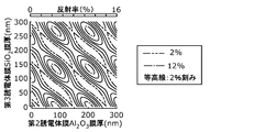
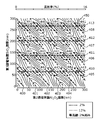
- FIG. 6A is a graph showing the reflectance with respect to the film thickness before aging of the dielectric multilayer film 150 included in the nitride semiconductor laser device 10 according to the embodiment.
- FIG. 6B is a graph showing the reflectance with respect to the film thickness after aging of the dielectric multilayer film 150 included in the nitride semiconductor laser device 10 according to the embodiment.
- FIG. 6C is a graph showing the amount of change in reflectance with respect to the film thickness before and after aging of the dielectric multilayer film 150 included in the nitride semiconductor laser device 10 according to the embodiment.
- FIGS. 6A to 6C conditions such as the film thickness and the refractive index of the first dielectric film 120 are fixed. Further, in FIGS. 6A to 6C, the second dielectric film 130 is an Al 2 O 3 film, and the third dielectric film 140 is a SiO 2 film. In FIGS. 6A to 6C, the film thickness of these films is changed in the range of 0 nm to 300 nm, the reflectance is calculated, and contour lines are displayed.
- the film thickness shown in FIG. 6B indicates the film thickness before aging. Specifically, the graph shown in FIG. 6B shows that the film thickness of the second dielectric film 130 is ⁇ 7.6% of the film thickness of the second dielectric film 130 and the third dielectric film 140 before aging. Then, the reflectance when the film thickness of the third dielectric film 140 is + 4.6% is calculated and displayed as contour lines.
- FIG. 6C shows the calculation result of the difference in reflectance before and after aging. Specifically, the graph shown in FIG. 6C shows a value obtained by subtracting the reflectance of the graph shown in FIG. 6B from the reflectance of the graph shown in FIG. 6A.
- contour lines are shown in increments of + 3% for the amount of change on the positive side of the reflectance from + 1.5%, and the amount of change on the negative side of the reflectance is -3% in order from -1.5%. Contour lines are shown in increments.
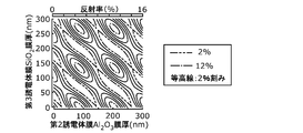
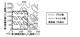
- FIG. 7 is a diagram for explaining the relationship between the film thickness of the second dielectric film 130 and the third dielectric film 140 and the reflectance of the dielectric multilayer film 150.
- the graph showing the reflectance with respect to the film thickness shown in FIG. 7 is the same as that in FIG. 6A.
- One or more protective films (four protective films in the present embodiment) in the first dielectric film 120 are applied in order from the front end surface 100F side to the first protective film, the second protective film, ...
- the n-layer film of the n-protective film is used, and the refractive index and the film thickness of the k-th protective film (k is a positive integer) are nk and dk, respectively, and the refractive index and the film thickness of the second dielectric film 130 are defined.
- Ni and di, respectively, the refractive index and the film thickness of the third dielectric film 140 are nj and dj, respectively, and the sum of the optical film thicknesses of one or more protective films in the first dielectric film 120 is A. Then, the following equation (1) is satisfied.
- broken lines 400 to 407 shown in FIG. 7 satisfy the following formula (2) in order from the left side of the paper.
- m1 is a positive integer.
- the reflectance of the dielectric multilayer film 150 takes a maximum value when m1 is an even number, and becomes a minimum value when m1 is an odd number.
- the change between the maximum and the minimum reflectance of the dielectric multilayer film 150 is a film having a relational expression between the optical film thickness and the reflectance of the SiO 2 film, which is the third dielectric film 140 derived from Fresnel's equation.
- the period coincides with cos (4 ⁇ ⁇ nj ⁇ dj / ⁇ ), which is a proportional term of thickness. That is, the multiplication (that is, the optical film thickness) between the film thickness of the third dielectric film 140 and the refractive index at which the reflectance of the dielectric multilayer film 150 is maximized or minimized satisfies the following equation (3).
- the optical refractive index and film thickness of the third dielectric film 140 are nj and dj, respectively.
- the relationship between the optical film thickness of the second dielectric film 130 and the reflectance is such that although the period between the maximum and the minimum is ⁇ / 4, the optical film thickness that becomes the maximum or the minimum is the first dielectric film. It is not necessarily an integral multiple of ⁇ / 4 because it is affected by the film thickness of 120.
- the film thickness and the refractive index of the second dielectric film 130 which maximizes or minimizes the reflectance of the dielectric multilayer film 150, satisfy the following formula (5).
- the refractive index and the film thickness of the second dielectric film 130 are ni and di, respectively.
- N2 is a positive integer.
- D becomes a broken line 420.
- B becomes a broken line 421.
- B becomes a broken line 422.
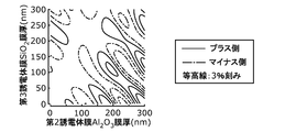
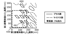
- 8A to 8F are graphs showing the reflectance with respect to the film thickness before aging of the dielectric multilayer film 150 included in the nitride semiconductor laser device 10 according to the embodiment.
- 9A to 9F are graphs showing the amount of change in reflectance with respect to the film thickness before and after aging of the dielectric multilayer film 150 included in the nitride semiconductor laser device 10 according to the embodiment.
- FIGS. 8A and 9A are graphs when the optical film thickness of the first dielectric film 120 is ⁇ / 8.
- 8B and 9B are graphs when the optical film thickness of the first dielectric film 120 is 3 ⁇ ⁇ / 16.
- 8C and 9C are graphs when the optical film thickness of the first dielectric film 120 is ⁇ / 4.
- 8D and 9D are graphs when the optical film thickness of the first dielectric film 120 is 5 ⁇ ⁇ / 16.
- 8E and 9E are graphs when the optical film thickness of the first dielectric film 120 is 3 ⁇ ⁇ / 8.
- 8F and 9F are graphs when the optical film thickness of the first dielectric film 120 is ⁇ / 2.
- ⁇ indicates the oscillation wavelength of the laser beam 201, which is 400 nm in the present embodiment.
- contour lines are shown in increments of + 3% in order from + 1.5% for the amount of change on the positive side of the reflectance, and in order from -1.5% for the amount of change on the negative side of the reflectance. Contour lines are shown in -3% increments.
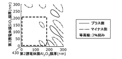
- the amount of change in reflectance is about ⁇ 1.5% or more and + 1.5% or less within the broken line 430.
- the broken line 430 indicates a range in which the film thickness of the second dielectric film 130 is 3 ⁇ ⁇ / 4 or less and the film thickness of the third dielectric film 140 is 3 ⁇ ⁇ / 4 or less.
- the optical film thickness of the first dielectric film 120 (more specifically, the total optical film thickness of the plurality of protective films of the first dielectric film 120) is 3 ⁇ ⁇ / 16 or more and 5 ⁇ .
- the first film thickness is ⁇ / 16 or less
- the optical film thickness of the second dielectric film 130 is 3 ⁇ ⁇ / 4 or less
- the optical film thickness of the third dielectric film 140 is 3 ⁇ ⁇ / 4 or less.
- a plurality of nitride semiconductor laser devices 10 in which the dielectric multilayer film 150 is formed on the laminated structure 100 are manufactured, a plurality of nitride semiconductor lasers are manufactured due to manufacturing variations even if the dielectric multilayer film 150 is manufactured with the same film thickness.
- the film thicknesses of the respective dielectric multilayer films 150 of the element 10 do not completely match.
- FIG. 10 is a diagram for explaining the relationship between the film thickness of the dielectric multilayer film 150 and the film thickness variation of the dielectric multilayer film 150.
- the graph showing the reflectance with respect to the film thickness shown in FIG. 10 is the same as that in FIG. 6A.
- the change in the reflectance with respect to the change in the film thickness of the dielectric multilayer film 150 is considered to be small, that is, stable.
- the maximum value, the minimum value, and the saddle point of the reflectance in the graph shown in FIG. 10 are the intersection points 440 to 443 between any of the broken lines 400 to 404 shown in FIG. 10 and any of the broken lines 410 to 413.
- the maximum value, the minimum value, and the saddle point of the reflectance in the graph shown in FIG. 10 are film thicknesses satisfying the above formula (1) and the above formula (3).
- the reflectance when A in the above equation (1) is an even number and B in the above equation (3) is an even number, the reflectance shows a maximum and becomes one of a plurality of intersections 440. Further, for example, when A in the above equation (1) is an even number and B in the above equation (3) is an odd number, the reflectance indicates a saddle point and is any of a plurality of intersection points 441. For example, when A in the above equation (1) is an odd number and B in the above equation (3) is an even number, the reflectance indicates a saddle point and is any of a plurality of intersections 442. For example, when A in the above equation (1) is an odd number and B in the above equation (3) is an even number, the reflectance indicates a minimum and becomes any of a plurality of intersections 443.
- the reflectance of the dielectric multilayer film 150 it is preferable to select the intersection points 440 or 443 in order to realize a high reflectance, and it is preferable to select the intersection points 441 or 442 in order to realize a low reflectance. ..
- the change in reflectance can be reduced with respect to the change in the film thickness of the dielectric multilayer film 150.
- the change in reflectance can be reduced with respect to the change in the film thickness of the dielectric multilayer film 150.
- the region surrounded by the broken line 450 satisfies the following equations (7) and (8).
- n1 and m2 are both positive integers.
- the change in reflectance can be reduced with respect to the change in the film thickness of the dielectric multilayer film 150.
- m1 an integer of 2 or more
- the change in reflectance can be further reduced with respect to the change in the film thickness of the dielectric multilayer film 150.
- m2 1, in other words, by using the following equation (9), the change in reflectance can be further reduced with respect to the change in the film thickness of the dielectric multilayer film 150.
- m3 is a positive integer.
- the change (change) in the reflectance of the dielectric multilayer film 150 is suppressed. can. Therefore, fluctuations in the light output during driving of the nitride semiconductor laser device 10 and deterioration of the nitride semiconductor laser device 10 can be suppressed.
- the amount of change in the reflectance of the dielectric multilayer film 150 can be reduced even when aging is performed, and the amount of change in the reflectance of the dielectric multilayer film 150 can be reduced.
- the change in reflectance can be reduced with respect to the change in the film thickness of the dielectric multilayer film 150. That is, according to the nitride semiconductor laser device 10 including the dielectric multilayer film 150 that satisfies the above-mentioned first film thickness condition and the above-mentioned second film thickness condition, the change in optical characteristics can be suppressed.
- FIGS. 11A to 11F are graphs showing the amount of change in reflectance with respect to the film thickness before and after aging of the dielectric multilayer film 150 included in the nitride semiconductor laser device 10 according to the embodiment.
- the graphs showing the reflectance with respect to the film thickness shown in FIGS. 11A to 11F are the same as those in FIGS. 9A to 9F.
- the change in reflectance can be reduced with respect to the change in the film thickness of the dielectric multilayer film 150.
- the amount of change in the reflectance of the dielectric multilayer film 150 can be reduced even when aging is performed. That is, if it is within the range of the region surrounded by the broken line 430 and within the range of the region surrounded by the broken line 450 shown in FIGS. 11B to 11D, the change in the optical characteristics of the dielectric multilayer film 150 is changed. It can be suppressed more.
- FIG. 12 is a graph showing the reflectance of the dielectric multilayer film 150 with respect to the wavelength of the nitride semiconductor laser device 10 according to the embodiment.
- the graph shown in FIG. 12 is within the condition of the film thickness of the dielectric multilayer film 150 at the position 461 shown in FIG. 11C, that is, within the range of the region surrounded by the broken line 430 and surrounded by the broken line 450.
- the reflectance of the dielectric multilayer film 150 that satisfies the condition of the film thickness within the range of the region is shown.
- the graph shown in FIG. 3 is outside the range of the film thickness condition of the dielectric multilayer film 150 at the position 460 shown in FIG. 11B, that is, the region surrounded by the broken line 430, and is surrounded by the broken line 450.
- the reflectance of the dielectric multilayer film satisfying the condition of the film thickness outside the range of the region is shown.
- the reflectance of the dielectric multilayer film 150 satisfying the above-mentioned first film thickness condition and the above-mentioned second film thickness condition is almost the same before and after aging with respect to light having a wavelength of, for example, 400 nm. It can be seen that there is no change.
- the nitride semiconductor laser device 10 is composed of a plurality of semiconductor layers (for example, the first semiconductor layer 102, the active layer 103, and the second semiconductor layer 104) including the waveguide 110 and faces each other.
- the body multilayer film 150 is provided.
- the dielectric multilayer film 150 has a first dielectric film 120, a second dielectric film 130, and a third dielectric film 140 in this order from the resonator end face side.
- the first dielectric film 120 is composed of n (n is a positive integer) layer protective film from the first protective film to the nth protective film in order from the resonator end face side.
- the refractive index and the film thickness of the k (k is an integer satisfying 1 ⁇ k ⁇ n) th protective film in the first dielectric film 120 are nk and dk, respectively, and the second dielectric is used.
- the refractive index and film thickness of the body film 130 are ni and di, respectively, the refractive index and film thickness of the third dielectric film 140 are nj and dj, respectively, m1 is an integer of 2 or more, and m2 is positive.
- the film thickness and the refractive index of each film included in the dielectric multilayer film 150 are appropriately combined to form the film of the dielectric multilayer film 150. Even if the thickness fluctuates, the fluctuation of the reflectance can be suppressed to a small extent. Therefore, fluctuations in the light output during driving of the nitride semiconductor laser device 10 and deterioration of the nitride semiconductor laser device 10 can be suppressed. That is, according to the nitride semiconductor laser device 10, deterioration of optical characteristics can be suppressed.
- the nitride semiconductor laser device 10 satisfies the above formula (7) and also satisfies the above formula (8).
- one of the second dielectric film 130 and the third dielectric film 140 has a property that the film thickness is reduced by the laser light 201 emitted from the nitride semiconductor laser device 10, and the other is a nitride semiconductor laser. It has a property that the film thickness is increased by the laser light 201 emitted from the element 10.
- the film thickness and the refractive index of each film included in the dielectric multilayer film 150 are appropriately combined to form the film of the dielectric multilayer film 150. Even if the thickness fluctuates, the fluctuation of the reflectance can be suppressed to a small extent. Therefore, fluctuations in the light output during driving of the nitride semiconductor laser device 10 and deterioration of the nitride semiconductor laser device 10 can be suppressed.
- a recess 131 is formed in the second dielectric film 130 at the interface between the second dielectric film 130 and the third dielectric film 140 in response to the laser light 201 emitted from the end face of the resonator.
- the convex portion 141 is formed on the third dielectric film 140.
- the amount of change in the total film thickness of the dielectric multilayer film 150 can be reduced even when the laser beam 201 is irradiated. Therefore, the change in the reflectance of the dielectric multilayer film 150 is further suppressed.
- the change in the film thickness of the second dielectric film 130 and the third dielectric film 140 occurs in the optical path of the laser beam 201 emitted from the end face of the resonator.
- the change in the film thickness of the dielectric multilayer film 150 occurs on the optical path of the laser light 201, the amount of change in the total film thickness of the dielectric multilayer film 150 in the region through which the laser light 201 passes is reduced. .. Therefore, the change in the reflectance of the dielectric multilayer film 150 is further suppressed.
- the third dielectric film 140 has an amorphous structure.
- a third dielectric film 140 having a property of taking in a rare gas such as Ar contained in the second dielectric film 130 to increase the film thickness is realized.
- the nitride semiconductor laser device 10 further satisfies the above equation (9).
- the amount of change in the total film thickness of the dielectric multilayer film 150 can be reduced even when the laser beam 201 is irradiated. Therefore, the change in the reflectance of the dielectric multilayer film 150 is further suppressed.
- the oscillation wavelength of the nitride semiconductor laser device 10 is 420 nm or less.
- the configuration of the dielectric multilayer film 150 is as an end face coating film in the nitride semiconductor laser device 10 that emits a laser beam 201 having a wavelength of 420 nm or less, which is a wavelength at which the dielectric multilayer film 150 easily absorbs the laser beam 201. , Especially effective.
- the nitride semiconductor laser element 10 emits a laser beam 201 of 1 W or more.
- the change in the film thickness of the dielectric multilayer film 150 largely depends on the light output of the laser beam 201.
- the change in the film thickness of the dielectric multilayer film 150 is remarkably observed in the laser light 201 having an optical output of 1 W or more. Therefore, the configuration of the dielectric multilayer film 150 is particularly effective as an end face coating film in the nitride semiconductor laser device 10 that emits a laser beam 201 of 1 W or more that easily affects the film thickness of the dielectric multilayer film 150. ..
- the nitride semiconductor laser device 10 satisfies the above equation (10) when m3 is a positive integer.
- the amount of change in the total film thickness of the dielectric multilayer film 150 can be reduced even when the laser beam 201 is irradiated. Therefore, the change in the reflectance of the dielectric multilayer film 150 is further suppressed.
- the second dielectric film 130 is either Al 2 O 3 , Ta 2 O 5 , or ZrO 2
- the third dielectric film 140 is SiO 2 , B 2 O 3 , P 2. It is either O 5 or GeO 2.
- the dielectric multilayer film 150 a film whose film thickness decreases and a film whose film thickness increases by absorbing the laser beam 201 can be combined. Therefore, fluctuations in the light output during driving of the nitride semiconductor laser device 10 and deterioration of the nitride semiconductor laser device 10 can be suppressed.
- an aluminum nitride film is arranged between the resonator end face and the dielectric multilayer film 150.
- the aluminum nitride film can suppress the oxidation of the resonator end face in the nitride semiconductor laser device 10. Further, according to this, the dangling bond in the resonator end face and the dielectric multilayer film 150 can be reduced. Therefore, for example, even when the nitride semiconductor laser device 10 is driven so as to have a high light output, the deterioration of the dielectric multilayer film 150 can be suppressed.
- the aluminum nitride film contains crystalline aluminum nitride.
- the aluminum oxynitride film may be polycrystalline aluminum nitride, or may be a film containing a large amount of oxygen at the grain boundaries of the polycrystalline aluminum nitride.
- the oxidation of the resonator end face in the nitride semiconductor laser device 10 can be further suppressed by the inclusion of crystals in the aluminum nitride film. Further, according to this, the dangling bond in the resonator end face and the dielectric multilayer film 150 can be further reduced. Therefore, for example, even when the nitride semiconductor laser device 10 is driven so as to have a high light output, the deterioration of the dielectric multilayer film 150 can be further suppressed.
- a film composed of at least one of aluminum nitride yttrium and aluminum nitride lantern is arranged.
- This also makes it possible to suppress the oxidation of the resonator end face in the nitride semiconductor laser device 10 as in the case of the aluminum nitride film. Further, according to this, the dangling bond in the resonator end face and the dielectric multilayer film 150 can be reduced. Therefore, for example, even when the nitride semiconductor laser device 10 is driven so as to have a high light output, the deterioration of the dielectric multilayer film 150 can be suppressed.
- the nitride semiconductor laser device of the present disclosure is used, for example, as a light source for industrial lighting, facility lighting, industrial laser equipment such as in-vehicle head lamps and laser processing machines, and image display devices such as laser displays and projectors. can do.
- Dielectric semiconductor laser element 100 Laminated structure 100a First conductive semiconductor layer 100b Second conductive semiconductor layer 100F Front side end face 100R Rear side end face 101 Substrate 102 First semiconductor layer 103 Active layer 104 Second semiconductor layer 105 Contact layer 106 Insulation layer 107 2nd electrode 108 Pad electrode 109 1st electrode 110 waveguide 120 1st dielectric film 121 1st protective film 122 2nd protective film 123 3rd protective film 124 4th protective film 130 2nd dielectric film 131 Concave 140 Third dielectric film 141 Convex 150 Dielectric multilayer film 160 Coat film 200 Optical axis 201 Laser light 300, 301, d1, d2, d3, d4, di, dj Film thickness 400-408, 410-413, 420 ⁇ 423, 430, 450 Broken line 440 ⁇ 443 Intersection 460, 461 Position
Landscapes
- Physics & Mathematics (AREA)
- Condensed Matter Physics & Semiconductors (AREA)
- General Physics & Mathematics (AREA)
- Electromagnetism (AREA)
- Optics & Photonics (AREA)
- Semiconductor Lasers (AREA)
Abstract
窒化物半導体レーザ素子(10)は、積層構造体(100)と、誘電体多層膜(150)と、を備える。誘電体多層膜(150)は、共振器端面側から第1誘電体膜(120)、第2誘電体膜(130)、及び、第3誘電体膜(140)をこの順に有する。窒化物半導体レーザ素子(10)は、 (I)を満たし、nj×dj=m2×λ/4±λ/16を満たし、且つ、 (II)を満たす。
Description
本開示は、窒化物半導体レーザ素子に関する。
従来、レーザ光を出射する半導体レーザ素子における、端面(フロント側端面及びリア側端面)には、レーザ光を半導体レーザ素子の内部で共振させるため、及び、共振されたレーザ光を半導体レーザ素子から適切に出射させるために、反射膜が形成されている(例えば、特許文献1参照)。
半導体レーザ素子の端面に形成される反射膜は、半導体レーザ素子からのレーザ光を吸収することで、変形する場合がある。反射膜は、変形することでレーザ光の透過率及び反射率が変動する等の光学特性が変化してしまう。
本開示は、光学特性の変化を抑制できる窒化物半導体レーザ素子を提供する。
本開示の一態様に係る窒化物半導体レーザ素子は、導波路を含む複数の半導体層からなり、互いに対向する一対の共振器端面を有する積層構造体と、前記一対の共振器端面の少なくとも一方に配置された誘電体多層膜と、を備える窒化物半導体レーザ素子であって、前記誘電体多層膜は、前記共振器端面側から第1誘電体膜、第2誘電体膜、及び、第3誘電体膜をこの順に有し、前記第1誘電体膜は、前記共振器端面側から順に第1保護膜から第n保護膜までのn(nは正の整数)層の保護膜で構成され、前記第1誘電体膜におけるk(kは1≦k≦nを満たす整数)番目の保護膜の屈折率と膜厚とを、それぞれnkとdkとし、前記第2誘電体膜の屈折率と膜厚とを、それぞれniとdiとし、前記第3誘電体膜の屈折率と膜厚とを、それぞれnjとdjとし、m1を2以上の整数とし、m2を正の整数とした場合、

を満たし、nj×dj=m2×λ/4±λ/16を満たし、且つ、

を満たす。
また、本開示の別の一態様に係る窒化物半導体レーザ素子は、導波路を含む複数の半導体層からなり、互いに対向する一対の共振器端面を有する積層構造体と、前記一対の共振器端面の少なくとも一方に配置された誘電体多層膜と、を備える窒化物半導体レーザ素子であって、前記誘電体多層膜は、前記共振器端面側から第1誘電体膜、第2誘電体膜、及び、第3誘電体膜をこの順に有し、前記第1誘電体膜は、前記共振器端面側から順に第1保護膜から第n保護膜までのn(nは正の整数)層の保護膜で構成され、前記第1誘電体膜におけるk(kは1≦k≦nを満たす整数)番目の保護膜の屈折率と膜厚とを、それぞれnkとdkとし、前記第2誘電体膜の屈折率と膜厚とを、それぞれniとdiとし、前記第3誘電体膜の屈折率と膜厚とを、それぞれnjとdjとし、m1を2以上の整数とし、m2を正の整数とした場合、

を満たし、且つ、nj×dj=m2×λ/4±λ/16を満たし、前記第2誘電体膜及び前記第3誘電体膜の一方は、前記窒化物半導体レーザ素子から出射されたレーザ光により膜厚が減少する性質を有し、他方は、前記窒化物半導体レーザ素子から出射されたレーザ光により膜厚が増加する性質を有する。
本開示によれば、光学特性の変化を抑制できる窒化物半導体レーザ素子を提供できる。
以下、本開示の実施の形態について、図面を参照しながら説明する。なお、以下に説明する実施の形態は、いずれも本開示の一具体例を示すものである。したがって、以下の実施の形態で示される、数値、形状、材料、構成要素、及び、構成要素の配置位置や接続形態などは、一例であって本開示を限定する主旨ではない。
また、各図は模式図であり、必ずしも厳密に図示されたものではない。したがって、各図において縮尺等は必ずしも一致していない。なお、各図において、実質的に同一の構成に対しては同一の符号を付しており、重複する説明は省略又は簡略化する。
また、本明細書において、「上方」及び「下方」という用語は、絶対的な空間認識における上方向(鉛直上方)及び下方向(鉛直下方)を指すものではなく、積層構成における積層順を基に相対的な位置関係により規定される用語として用いる。また、「上方」及び「下方」という用語は、2つの構成要素が互いに間隔をあけて配置されて2つの構成要素の間に別の構成要素が存在する場合のみならず、2つの構成要素が互いに接する状態で配置される場合にも適用される。
また、本明細書及び図面において、X軸、Y軸及びZ軸は、三次元直交座標系の三軸を示している。各実施の形態では、Z軸方向を鉛直方向とし、Z軸に垂直な方向(XY平面に平行な方向)を水平方向としている。なお、Z軸の正方向を鉛直上方としている。
(実施の形態)
[概要]
図1は、実施の形態に係る窒化物半導体レーザ素子10の構成を示す模式的な断面図である。図2は、実施の形態に係る窒化物半導体レーザ素子10がレーザ光201を出射した場合の誘電体膜の変形の一例を模式的に示す断面図である。なお、図1と図2と、は後述する図4のI-I線における断面図である。
[概要]
図1は、実施の形態に係る窒化物半導体レーザ素子10の構成を示す模式的な断面図である。図2は、実施の形態に係る窒化物半導体レーザ素子10がレーザ光201を出射した場合の誘電体膜の変形の一例を模式的に示す断面図である。なお、図1と図2と、は後述する図4のI-I線における断面図である。
窒化物半導体レーザ素子10は、第1導電型半導体層100aと、第2導電型半導体層100bと、第1導電型半導体層100aと第2導電型半導体層100bとの間に挟まれたレーザ光201を出射する活性層103と、を有する積層構造体100を備える。窒化物半導体レーザ素子10のフロント側端面100Fには、積層構造体100の内部でレーザ光201を共振させてフロント側端面100Fから効果的に出射させるために、誘電体多層膜150が形成されている。誘電体多層膜150は、例えば、第1誘電体膜120と、第2誘電体膜130と、第3誘電体膜140と、からなる。具体的には、積層構造体100のフロント側端面100Fには、第1誘電体膜120と、第2誘電体膜130と、第3誘電体膜140とがこの順で配置されている。
第1誘電体膜120は、フロント側端面100Fを保護する膜であり、外部からの酸素の拡散によるフロント側端面100Fの酸化を抑制する。第2誘電体膜130と第3誘電体膜140とは、それぞれ、反射率を調整するための膜である。
第1誘電体膜120と第2誘電体膜130と第3誘電体膜140とは、フロント側端面100Fに膜厚がほぼ均一に形成されている。
従来、誘電体多層膜150の反射率の設計を行うに際し、誘電体多層膜150の膜厚分布を考慮する必要はなく、積層構造体100から出射されるレーザ光201の発振波長に対して極大又は極小となるよう誘電体多層膜150の膜厚及び材料の設計を行っていた。
近年、発振波長が405nm程度であり、且つ、レーザ光201の光出力が1W以上である青紫高出力レーザ素子がある。本願発明者らは、このような青紫高出力レーザ素子において、長時間エージングを行う(つまり、レーザ光201を出射させ続ける)と、フロント側端面100Fにおけるレーザ光201が出射される部分(発光点)近傍の誘電体多層膜150の膜が変質することを見出した。
例えば、図2に示すように、第2誘電体膜130と第3誘電体膜140とは、積層構造体100から出射されたレーザ光201を吸収することで、変形する場合がある。
例えば、積層構造体100からレーザ光201を出射させることで、第2誘電体膜130と第3誘電体膜140とのそれぞれの膜厚は、レーザ光201が通過する部分の膜厚300と、レーザ光201が通過しない部分の膜厚301とで、異なる。つまり、第2誘電体膜130と第3誘電体膜140とのそれぞれの膜厚300、301は、レーザ光201を積層構造体100から出射させることで変化する。
図3は、比較例に係る窒化物半導体レーザ素子の波長に対する誘電体多層膜の反射率を示すグラフである。比較例に係る窒化物半導体レーザ素子は、実施の形態に係る窒化物半導体レーザ素子10と、誘電体多層膜に採用される材料、膜厚、及び、屈折率以外は同様である。また、図3に示すエージング前の反射率とは、例えば、図1に示す誘電体多層膜150のように、レーザ光201によって変形していない状態における光の反射率である。一方、図3に示すエージング後の反射率とは、例えば、図2に示す誘電体多層膜150のように、レーザ光201によって変形した状態における光の反射率である。
図3に示すように、エージング前の反射率とエージング後の反射率とで、波長が400nm付近に位置するピークの位置が異なる。具体的には、比較例に係る誘電体多層膜の反射率は、レーザ光を吸収することで、波長が400nm付近に位置するピークの反射率が1.5%程度上昇する。そのため、比較例に係る窒化物半導体レーザ素子は、エージング前とエージング後とで光学特性(具体的には、光出力)が異なる。したがって、例えば、窒化物半導体レーザ素子10を使用し続けると、時間経過に伴い光学特性が変化する。
本願発明者らは、鋭意検討した結果、窒化物半導体レーザ素子10が備える誘電体多層膜150の材料、膜厚、及び、屈折率等を適切に設定することにより、光学特性の変化を抑制できることを見出した。具体的には、本願発明者らは、エージング中に膜厚が増加する膜と減少する膜とがあることを見出した。そこで、本願発明者らは、エージング中に膜厚が増加する膜と減少する膜とを適切に組み合わせる事により、エージング中に膜厚が変化しても反射率の変化を抑制できることを見出した。
以下、実施の形態に係る窒化物半導体レーザ素子10の構成及び光学特性について具体的に説明する。
なお、以下の説明においては、積層構造体100からレーザ光201を出射させることを単にエージングともいう。
[構成]
図1及び図4を参照しながら、窒化物半導体レーザ素子10の構成について説明する。
図1及び図4を参照しながら、窒化物半導体レーザ素子10の構成について説明する。
図4は、図1のIV-IV線における、実施の形態に係る窒化物半導体レーザ素子10を示す断面図である。
窒化物半導体レーザ素子10は、レーザ光201を出射する窒化物半導体発光素子である。
窒化物半導体レーザ素子10は、積層構造体100と、誘電体多層膜150とを備える。
積層構造体100は、導波路110を含む複数の半導体層からなる積層体である。また、積層構造体100は、互いに対向する一対の共振器端面であるフロント側端面100Fと、リア側端面100Rとを有する。誘電体多層膜150は、当該一対の共振器端面の少なくとも一方に配置されている。本実施の形態では、フロント側端面100Fに誘電体多層膜150が配置されている。
積層構造体100は、基板101と、第1半導体層102と、活性層103と、第2半導体層104と、コンタクト層105と、絶縁層106と、第2電極107と、パッド電極108と、第1電極109と、を有する。図1における第1導電型半導体層100aは、基板101と第1半導体層102とを含み、第2導電型半導体層100bは、第2半導体層104と、コンタクト層105とを含む。なお、図1では、絶縁層106と、第2電極107と、パッド電極108と、第1電極109とは、図示が省略されている。本実施の形態では、積層構造体100は、窒化物材料の一例である窒化ガリウム系材料で形成される。これにより、例えば、積層構造体100への投入電流を2A以上10A以下とし、投入電圧を4V以上6V以下とすることで、390nm以上420nm以下程度の帯域の波長を有し、且つ、光出力が3W以上10W以下程度であるレーザ光201を出射する光学特性を有する窒化物半導体レーザ素子10を実現できる。このように、本実施の形態では、窒化物半導体レーザ素子10は、1W以上のレーザ光201を出射する。また、窒化物半導体レーザ素子10の発振波長は、420nm以下である。より具体的には、積層構造体100は、ピーク波長が400nmのレーザ光201を出射する。
また、例えば、レーザ光201の光学密度は、0.1W/μm以上である。なお、光学密度とは、レーザ光201の光出力/ストライプ幅である。ここでのストライプ幅は、例えば、後述するリッジ部の横幅(本実施の形態では、X軸方向の長さ)である。リッジ部の幅(以下、ストライプ幅ともいう)は、例えば、30μm以上100μm以下程度である。
積層構造体100の共振器長(本実施の形態では、Y軸方向の長さ)は、例えば、1200μm以上5000μm以下である。
なお、窒化物半導体レーザ素子10の光学特性は、上記に限定されない。例えば、窒化物半導体レーザ素子10は、積層構造体100への投入電流を2A以上10A以下とし、投入電圧を3.5V以上6V以下とすることで、365nm以上390nm以下程度の帯域の波長を有し、且つ、光出力が1W以上5W以下程度であるレーザ光201を出射する光学特性を有してもよい。この場合、例えば、ストライプ幅は、8μm以上100μm以下程度である。また、この場合、例えば、積層構造体100の共振器長は、例えば、800μm以上5000μm以下である。
基板101は、積層構造体100の基材となる板状部材である。本実施の形態では、基板101は、厚さ100μmのGaN単結晶基板である。なお、基板101の厚さは、100μmに限定されず、例えば、50μm以上、120μm以下であってもよい。また、基板101を形成する材料は、GaN単結晶に限定されず、サファイア、SiC等であってもよい。
第1半導体層102は、基板101の上方に配置される第1導電型の半導体層である。本実施の形態では、第1半導体層102は、基板101の一方の主面に配置されるn型の半導体層であり、n型クラッド層が含まれる。n型クラッド層は、n-AlGaNからなる層である。なお、n型クラッド層の構成はこれに限定されない。
活性層103は、第1半導体層102の上方に配置される発光層である。本実施の形態では、活性層103は、InGaNからなる井戸層と、GaNからなる障壁層とが交互に積層された量子井戸活性層であり、二層の井戸層を有する。このような活性層103を備えることにより、窒化物半導体レーザ素子10は、波長が約400nmの青色レーザ光を出射できる。活性層103の構成はこれに限定されず、井戸層と障壁層とが交互に積層された量子井戸活性層であればよい。なお、活性層103は、量子井戸活性層の上方及び下方の少なくとも一方に形成されたガイド層を含んでもよい。
第2半導体層104は、活性層103の上方に配置される第2導電型の半導体層である。第2導電型は、第1導電型と異なる導電型である。本実施の形態では、第2半導体層104は、p型の半導体層であり、p型クラッド層を含む。p型クラッド層は、p-AlGaNからなる層と、GaNからなる厚さ3nmの層とが交互に100層ずつ積層された超格子層である。なお、p型クラッド層の構成はこれに限定されない。
第1半導体層102と、活性層103と、第2半導体層104とによってレーザ光201の導波部である導波路110が形成される。
導波路110は、積層構造体100の内部でレーザ光201が導波する部分である。導波路110は、例えば、第1半導体層102の一部と、活性層103の一部と、第2半導体層104の一部とからなる。
コンタクト層105は、第2電極107とオーミック接触する第2導電型の半導体層である。本実施の形態では、コンタクト層105は、p型の半導体層であり、p-GaNからなる層である。なお、コンタクト層105の構成はこれに限定されない。
また、本実施の形態では、第2半導体層104及びコンタクト層105にリッジ部が形成されている。リッジ部に対応する活性層103の領域(つまり、リッジ部の下方に位置する活性層103の領域)が発光点となり、レーザ光201を出射する。
第1電極109は、基板101の下方の主面(つまり、第1半導体層102などが配置されていない方の主面)に配置される電極である。第1電極109は、例えば、基板101側から順にTi、Pt及びAuが積層された積層膜である。第1電極109の構成はこれに限定されない。
第2電極107は、コンタクト層105上に配置される電極である。本実施の形態では、第2電極107は、コンタクト層105とオーミック接触するp側電極である。当該p側電極上には、パッド電極108が配置されている。
第2電極107は、例えば、コンタクト層105側から順にPd及びPtが積層された積層膜である。第2電極107の構成はこれに限定されない。
パッド電極108は、第2電極107の上方に配置されたパッド状の電極である。パッド電極108は、例えば、第2電極107側から順にTi及びAuが積層された積層膜であり、リッジ部及その周辺に配置される。なお、パッド電極108の構成は、これに限定されない。
また、図4には示されないが、積層構造体100は、以上の各層の他に、リッジ部の側壁等を覆うSiO2膜等の絶縁膜等をさらに有してもよい。
なお、本実施の形態では、積層構造体100は、1個のリッジ部(エミッタ)を有する、いわゆるシングルエミッタであるが、複数の(例えば、60個程度の)リッジ部を有する、いわゆるマルチエミッタでもよい。この場合、例えば、積層構造体100における、複数のリッジ部のそれぞれの下方から出射されるレーザ光201の総光出力は、100W以上200W以下程度となる。
誘電体多層膜150は、積層構造体100のフロント側端面100Fに配置される保護膜である。具体的には、誘電体多層膜150は、積層構造体100のフロント側端面100Fを保護し、且つ、フロント側端面100Fにおけるレーザ光201の反射率を低減する。誘電体多層膜150は、共振器端面(本実施の形態では、フロント側端面100F)側から第1誘電体膜120と、第2誘電体膜130と、第3誘電体膜140とをこの順に有する。
第1誘電体膜120は、第1誘電体膜120、第2誘電体膜130、及び、第3誘電体膜140のうちで最もフロント側端面100F側に配置される誘電体層である。第1誘電体膜120は、窒化膜及び酸窒化膜の少なくとも一方からなる少なくとも1層の誘電体膜を含んでもよい。これにより、誘電体多層膜150の外側から積層構造体100への酸素拡散を低減できる。このため、積層構造体100のフロント側端面100Fの劣化を抑制できる。したがって、窒化物半導体レーザ素子10の長期動作が可能となる。
また、第1誘電体膜120は、積層構造体100のフロント側端面100Fに直接接続される。つまり、第1誘電体膜120は、フロント側端面100Fに接して形成される。このため、第1誘電体膜120として、積層構造体100と同様の結晶性を有する窒化膜又は酸窒化膜を用いることで、フロント側端面100Fの保護性能を高めることができる。
例えば、第1誘電体膜120は、フロント側端面100F側から順に第1保護膜から第n保護膜までのn(nは正の整数)層の保護膜で構成されている。本実施の形態では、第1誘電体膜120は、n=4であり、第1保護膜121と、第2保護膜122と、第3保護膜123と、第4保護膜124とを有する。
第1保護膜121は、第1誘電体膜120が有する複数の保護膜のうちで最もフロント側端面100F側に配置される誘電体膜である。本実施の形態では、第1保護膜121は、SiN膜を含む膜である。より具体的には、第1保護膜121は、厚さd1が0.5nm程度のSiN膜からなる膜である。なお、第1保護膜121の構成は、これに限定されない。第1保護膜121は、例えば、SiON等の他の酸窒化膜であってもよい。
第2保護膜122は、第1保護膜121に積層される誘電体膜である。本実施の形態では、第2保護膜122は、AlON膜を含む膜である。より具体的には、第2保護膜122は、厚さd2が21nm程度のAlON膜からなる膜である。なお、第2保護膜122の構成は、これに限定されない。第2保護膜122は、例えば、SiON等の他の酸窒化膜であってもよいし、AlN膜、SiN膜等の窒化膜であってもよい。
第3保護膜123は、第2保護膜122に積層される誘電体膜である。本実施の形態では、第3保護膜123は、厚さd3が13nm程度のAl2O3膜からなる膜である。なお、第3保護膜123の構成は、これに限定されない。第3保護膜123は、例えば、SiO2等の他の誘電体膜であってもよい。
第4保護膜124は、第3保護膜123に積層される誘電体膜である。第4保護膜124は、窒化膜及び酸窒化膜の少なくとも一方からなる誘電体膜を含んでもよい。本実施の形態では、第4保護膜124は、厚さd4が11nm程度のAlON膜からなる膜である。なお、第4保護膜124の構成は、これに限定されない。第4保護膜124は、例えば、SiN等の他の窒化膜であってもよいし、AlN膜、SiON膜等の酸窒化膜であってもよい。
第2誘電体膜130は、第1誘電体膜120の外側に積層される誘電体膜である。本実施の形態では、第2誘電体膜130は、厚さdiが167nm程度のAl2O3膜である。
第3誘電体膜140は、第2誘電体膜130の外側に積層される誘電体膜である。本実施の形態では、第3誘電体膜140は、厚さdjが58nm程度のSiO2膜である。
図5は、エージングの条件に対する膜厚の変化を示す表である。なお、条件1及び条件2のいずれにおいても、レーザ光201のピーク波長(発振波長)は405nmである。
図5の条件1に示すように、25℃で736h、積層構造体100から4.5Wのレーザ光201を出射させた場合、Al2O3膜からなる第2誘電体膜130の膜厚の変化率は、レーザ光201の光強度分布にばらつきがあり、最大で-8.5%であり、最小で-6.2%であった。また、条件1では、SiO2膜からなる第3誘電体膜140の膜厚の変化率は、最大で+5.3%であり、最小で3.7%であった。
なお、条件1における光学密度は、0.15(W/μm)である。
また、図5の条件2に示すように、25℃で4500h、積層構造体100から1Wのレーザ光201を出射させた場合、Al2O3膜からなる第2誘電体膜130の膜厚の変化率は、最大で-8.7%であり、最小で-7.0%であった。また、条件2では、SiO2膜からなる第3誘電体膜140の膜厚の変化率は、最大で+5.2%であり、最小で4.0%であった。
なお、条件2における光学密度は、0.149(W/μm)である。
条件1及び条件2における、Al2O3膜からなる第2誘電体膜130の膜厚の変化率は、平均で-7.6%であった。また、条件1及び条件2における、SiO2膜からなる第3誘電体膜140の膜厚の変化率は、平均で+4.6%であった。
また、Al2O3膜からなる第2誘電体膜130の膜厚の変化率は、光学密度が0.15W/μm程度では、エージング時間が1000h以内では急激に減少し、エージング時間が1000h以降では変化が緩やかになりながらも徐々に減少した。また、SiO2膜からなる第3誘電体膜140の膜厚の変化率は、光学密度が0.15W/μm程度では、エージング時間が1000h以内では急激に増加し、エージング時間が1000h以降では変化が緩やかになりながらも徐々に増加した。
以上のように、Al2O3膜からなる第2誘電体膜130は、エージングによって収縮して膜厚が減少する。Al2O3膜からなる膜は、成膜された直後の状態(as-depo.)ではArを数%含むアモルファスである。しかしながら、as-depo.のAl2O3膜からなる膜は、エージングによる光学的負荷によりArが脱離することで収縮して膜厚が減少すると考えられる。
一方、SiO2膜からなる第3誘電体膜140は、エージングによって膨張して膜厚が増加する。SiO2膜からなる第3誘電体膜140は、Al2O3膜からなる第2誘電体膜130に含まれていたArが脱離し、SiO2膜中に拡散することで膜が膨張して膜厚が増加したと考えられる。
このことから、エージングにより膜が膨張する材料としては、アモルファス状態が安定な材料、及び、分子結合に自由度があり内部に不純物原子を含みやすい材料が考えらえる。このような材料としては、SiO2、B2O3、P2O5、及び、GeO2が例示される。本実施の形態では、第3誘電体膜140は、アモルファス構造である。また、例えば、第3誘電体膜140は、SiO2、B2O3、P2O5、及び、GeO2のいずれかである。
また、エージングにより膜が収縮する材料としては、アモルファス状態よりも結晶状態が安定な材料、及び、原子間結合が強く内部に不純物原子を含みにくい材料が考えられる。このような材料としては、Al2O3、Ta2O5、及び、ZrO2が例示される。例えば、第2誘電体膜130は、Al2O3、Ta2O5、及び、ZrO2のいずれかである。
このように、第2誘電体膜130及び第3誘電体膜140の一方は、窒化物半導体レーザ素子10から出射されたレーザ光201により膜厚が減少する性質を有する。他方は、窒化物半導体レーザ素子10から出射されたレーザ光201により膜厚が増加する性質を有する。本実施の形態では、第2誘電体膜130は、窒化物半導体レーザ素子10から出射されたレーザ光201により膜厚が減少する性質を有する。第3誘電体膜140は、窒化物半導体レーザ素子10から出射されたレーザ光201により膜厚が増加する性質を有する。具体的には、フロント側端面100Fから出射されたレーザ光201を受けて、第2誘電体膜130と第3誘電体膜140との界面において、第2誘電体膜130には、凹部131が形成され、第3誘電体膜140には、凸部141が形成される。また、例えば、第2誘電体膜130及び第3誘電体膜140の膜厚の変化は、フロント側端面100Fから出射されたレーザ光201の光路(例えば、レーザ光201の光軸200上)で発生する。
このような材料で構成された誘電体多層膜150を備える窒化物半導体レーザ素子10によれば、誘電体多層膜150が後述するような膜厚及び屈折率を有することで、10000h程度レーザ光201を出射させても、光出力の低下率は20%以下となる。
なお、フロント側端面100Fと誘電体多層膜150との間には、コート膜160が配置されていてもよい。
コート膜160は、フロント側端面100Fを保護する膜であり、例えば、酸窒化アルミニウム膜である。当該酸窒化アルミニウム膜は、結晶の窒化アルミニウムを含んでもよい。具体的には、当該酸窒化アルミニウム膜は、結晶の窒化アルミニウムでもよい。
なお、コート膜160に採用される材料は、これに限定されない。例えば、コート膜160に採用される材料は、窒化アルミニウムシリコンと、窒化アルミニウムガリウムと、窒化アルミニウムイットリウムと、窒化アルミニウムランタンと、酸窒化アルミニウムシリコンと、酸窒化アルミニウムガリウムと、酸窒化アルミニウムイットリウムと、酸窒化アルミニウムランタンとの少なくとも1つでもよい。また、第1誘電体膜120の材料に、上記した材料が用いられてもよい。
また、このような誘電体多層膜150は、後述するような膜厚及び屈折率を有することで、例えば、波長が400nmの光に対する反射率が4%以上20以下程度となる。また、誘電体多層膜150にいわゆるAR(Anti Reflection)コートの技術を採用することで、誘電体多層膜150は、波長が400nmの光に対する反射率を0.1%以下としてもよい。
また、誘電体多層膜150は、リア側端面100Rに設けられてもよい。
[光学特性]
続いて、実施の形態に係る窒化物半導体レーザ素子10の光学特性について説明する。
続いて、実施の形態に係る窒化物半導体レーザ素子10の光学特性について説明する。
本願発明者らは、誘電体多層膜150において、膜厚が変化しても反射率の変化が少ない条件を決定するために、光学シミュレーションを実施した。以下の光学シミュレーションでは、第2誘電体膜130をAl2O3膜とし、第3誘電体膜140をSiO2膜としている。
図6Aは、実施の形態に係る窒化物半導体レーザ素子10が備える誘電体多層膜150のエージング前における、膜厚に対する反射率を示すグラフである。図6Bは、実施の形態に係る窒化物半導体レーザ素子10が備える誘電体多層膜150のエージング後における、膜厚に対する反射率を示すグラフである。図6Cは、実施の形態に係る窒化物半導体レーザ素子10が備える誘電体多層膜150のエージング前後における、膜厚に対する反射率の変化量を示すグラフである。
なお、図6A~図6Cにおいて、第1誘電体膜120の膜厚、屈折率等の条件は、固定している。また、図6A~図6Cでは、第2誘電体膜130をAl2O3膜とし、第3誘電体膜140をSiO2膜としている。図6A~図6Cでは、これらの膜の膜厚を0nm~300nmの範囲で変化させ、反射率を計算し、等高線表示している。
なお、図6Bに示す膜厚は、エージング前における膜厚を示している。具体的には、図6Bに示すグラフは、第2誘電体膜130及び第3誘電体膜140におけるエージング前の膜厚に対して、第2誘電体膜130の膜厚を-7.6%し、第3誘電体膜140の膜厚を+4.6%した場合における反射率を計算して等高線表示している。
また、図6Cは、エージング前後の反射率の差分の計算結果を示している。具体的には、図6Cに示すグラフは、図6Aに示すグラフの反射率から図6Bに示すグラフの反射率を減算した値を示している。
また、図6Cでは、反射率のプラス側の変化量について、+1.5%から順に+3%刻みで等高線を示し、反射率のマイナス側の変化量について、-1.5%から順に-3%刻みで等高線を示している。
図6Cから、エージング前後で反射率の変化量が-1.5%以上+1.5%以下となる領域があることがわかる。
図7は、第2誘電体膜130及び第3誘電体膜140の膜厚と誘電体多層膜150の反射率との関係を説明するための図である。なお、図7に示す膜厚に対する反射率を示すグラフは、図6Aと同じである。
第1誘電体膜120における1以上の保護膜(本実施の形態では、4つの保護膜)を、フロント側端面100F側から順に第1保護膜、第2保護膜、・・・、及び、第n保護膜のn層の膜とし、k(kは正の整数)番目の保護膜の屈折率と膜厚とを、それぞれnkとdkとし、第2誘電体膜130の屈折率と膜厚とを、それぞれniとdiとし、第3誘電体膜140の屈折率と膜厚とを、それぞれnjとdjとし、第1誘電体膜120における1以上の保護膜の光学膜厚の総和をAとすると、下記の式(1)を満たす。
また、図7に示す破線400~407は、紙面左側から順に、下記の式(2)を満たす。
A=m1×λ/4 式(2)
なお、m1は、正の整数である。例えば、破線400は、式(2)にm1=1を代入した場合の直線である。同様に、例えば、破線401は、式(2)にm1=2を代入した場合の直線である。同様に、例えば、破線402は、式(2)にm1=3を代入した場合の直線である。同様に、例えば、破線403は、式(2)にm1=4を代入した場合の直線である。同様に、例えば、破線404は、式(2)にm1=5を代入した場合の直線である。同様に、例えば、破線405は、式(2)にm1=6を代入した場合の直線である。同様に、例えば、破線406は、式(2)にm1=7を代入した場合の直線である。同様に、例えば、破線407は、式(2)にm1=8を代入した場合の直線である。
ここで、誘電体多層膜150の反射率は、m1が偶数の場合に極大値をとり、m1が奇数の場合に極小値となる。
また、誘電体多層膜150における反射率の極大と極小との変化は、フレネルの式より導出される第3誘電体膜140であるSiO2膜の光学膜厚と反射率との関係式の膜厚の比例項であるcos(4π×nj×dj/λ)と周期が一致している。すなわち、誘電体多層膜150の反射率が極大又は極小となる第3誘電体膜140の膜厚と屈折率との乗算(つまり、光学膜厚)は、下記の式(3)を満たす。
B=nj×dj=N1×λ/4 式(3)
なお、第3誘電体膜140の光学屈折率と膜厚とは、それぞれnj、djである。また、N1は、0又は正の整数である。例えば、N1=1の場合、Bは、破線410となる。また、例えば、N1=2の場合、Bは、破線411となる。また、例えば、N1=3の場合、Bは、破線412となる。また、例えば、N1=4の場合、Bは、破線413となる。
上記した式(3)は、第1誘電体膜120の膜厚を変化させても満たされる。
一方、第2誘電体膜130の光学膜厚と反射率との関係は、極大と極小との周期がλ/4となっているものの、極大又は極小となる光学膜厚が第1誘電体膜120の膜厚の影響を受けるため、必ずしもλ/4の整数倍ではない。
ここで、第1誘電体膜120と第2誘電体膜130との光学膜厚の総和をDとした場合、以下の式(4)を満たす。
また、誘電体多層膜150の反射率が極大又は極小となる第2誘電体膜130の膜厚と屈折率とは、下記の式(5)を満たす。
D=N2×λ/4 式(5)
なお、第2誘電体膜130の屈折率と膜厚とは、それぞれni、diである。また、N2は、正の整数である。例えば、N2=1の場合、Dは、破線420となる。また、例えば、N2=2の場合、Bは、破線421となる。また、例えば、N2=3の場合、Bは、破線422となる。また、例えば、N2=4の場合、Bは、破線423となる。また、例えば、N2=5の場合、Bは、破線424となる。
上記した式(5)は、第1誘電体膜120の膜厚と第2誘電体膜130の膜厚との比率を変化させても満たされる。
続いて、第1誘電体膜120の膜厚を変化させた場合における、膜厚の変化について説明する。
図8A~図8Fは、実施の形態に係る窒化物半導体レーザ素子10が備える誘電体多層膜150のエージング前における、膜厚に対する反射率を示すグラフである。図9A~図9Fは、実施の形態に係る窒化物半導体レーザ素子10が備える誘電体多層膜150のエージング前後における、膜厚に対する反射率の変化量を示すグラフである。
なお、図8A及び図9Aは、第1誘電体膜120の光学膜厚をλ/8とした場合のグラフである。また、図8B及び図9Bは、第1誘電体膜120の光学膜厚を3×λ/16とした場合のグラフである。また、図8C及び図9Cは、第1誘電体膜120の光学膜厚をλ/4とした場合のグラフである。また、図8D及び図9Dは、第1誘電体膜120の光学膜厚を5×λ/16とした場合のグラフである。また、図8E及び図9Eは、第1誘電体膜120の光学膜厚を3×λ/8とした場合のグラフである。また、図8F及び図9Fは、第1誘電体膜120の光学膜厚をλ/2とした場合のグラフである。
なお、λは、レーザ光201の発振波長を示し、本実施の形態では、400nmである。
また、図9A~図9Fでは、反射率のプラス側の変化量について、+1.5%から順に+3%刻みで等高線を示し、反射率のマイナス側の変化量について、-1.5%から順に-3%刻みで等高線を示している。
図9B、図9C、及び、図9Dに示すように、破線430内であれば、反射率の変化量が-1.5%以上+1.5%以下程度となることがわかる。破線430は、第2誘電体膜130の膜厚が3×λ/4以下であり、且つ、第3誘電体膜140の膜厚が3×λ/4以下である範囲を示す。
以上のことから、第1誘電体膜120の光学膜厚(より具体的には、第1誘電体膜120が有する複数の保護膜の光学膜厚の総和)を3×λ/16以上5×λ/16以下とし、第2誘電体膜130の光学膜厚を3×λ/4以下とし、且つ、第3誘電体膜140の光学膜厚が3×λ/4以下とする第1膜厚条件にすることで、エージングした場合においても、誘電体多層膜150の反射率の変化量を、-1.5%以上+1.5%程度以下とするように小さくすることができる。つまり、第1誘電体膜120は、以下の式(6)を満たす。
続いて、誘電体多層膜150の膜厚と誘電体多層膜150の膜厚ばらつきとの関係について説明する。
積層構造体100に誘電体多層膜150を形成した窒化物半導体レーザ素子10を複数製造すると、誘電体多層膜150を同じ膜厚で製造しようとしても製造ばらつきのために、複数の窒化物半導体レーザ素子10のそれぞれの誘電体多層膜150の膜厚は、完全には一致しない。
図10は、誘電体多層膜150の膜厚と誘電体多層膜150の膜厚ばらつきとの関係を説明するための図である。なお、図10に示す膜厚に対する反射率を示すグラフは、図6Aと同じである。
図10に示すグラフにおける反射率の極大値、極小値、及び、鞍点では、誘電体多層膜150の膜厚の変化に対する反射率の変化が小さい、つまり、安定であると考えられる。図10に示すグラフにおける反射率の極大値、極小値、及び、鞍点は、図10に示す破線400~404のいずれかと、破線410~413のいずれかとの交点440~443である。言い換えると、図10に示すグラフにおける反射率の極大値、極小値、及び、鞍点は、上記した式(1)と、上記した式(3)とを満たす膜厚である。
例えば、上記した式(1)におけるAが偶数であり、上記した式(3)におけるBが偶数の場合、反射率は極大を示し、複数の交点440のいずれかとなる。また、例えば、上記した式(1)におけるAが偶数であり、上記した式(3)におけるBが奇数の場合、反射率は鞍点を示し、複数の交点441のいずれかとなる。例えば、上記した式(1)におけるAが奇数であり、上記した式(3)におけるBが偶数の場合、反射率は鞍点を示し、複数の交点442のいずれかとなる。例えば、上記した式(1)におけるAが奇数であり、上記した式(3)におけるBが偶数の場合、反射率は極小を示し、複数の交点443のいずれかとなる。
ここで、誘電体多層膜150の反射率として、高い反射率を実現するためには交点440または443を選ぶのが良く、低い反射率を実現するためには交点441または442を選ぶのが良い。
以上のように、交点440~443の近傍であれば、誘電体多層膜150の膜厚の変化に対して反射率の変化を小さくできる。例えば、交点440~443の近傍を示す平行四辺形の破線450で囲まれた領域の範囲内であれば、誘電体多層膜150の膜厚の変化に対して反射率の変化を小さくできる。このような破線450で囲まれた領域は、下記の式(7)及び式(8)を満たす。
B1=nj×dj=m2×λ/4±λ/16 式(8)
なお、m1及びm2は、いずれも正の整数である。
このような第2膜厚条件とすることで、誘電体多層膜150の膜厚の変化に対して反射率の変化を小さくできる。また、m1を2以上の整数とすることで、誘電体多層膜150の膜厚の変化に対して反射率の変化をさらに小さくできる。また、例えば、m2=1とした場合、言い換えると、下記の式(9)とすることで、誘電体多層膜150の膜厚の変化に対して反射率の変化をさらに小さくできる。
3λ/16≦nj×dj≦5λ/16 式(9)
また、上記した式(4)と上記した(5)と交点440~443の近傍を示す平行四辺形の破線450で囲まれた領域との関係から、下記の式(10)が算出される。
なお、m3は、正の整数である。
これによれば、窒化物半導体レーザ素子10を駆動した際(窒化物半導体レーザ素子10にレーザ光201を出射させた際)にも、誘電体多層膜150の反射率の変動(変化)を抑制できる。そのため、窒化物半導体レーザ素子10の駆動中の光出力の変動、及び、窒化物半導体レーザ素子10の劣化を抑制できる。
以上のことから、上記した第1膜厚条件と、上記した第2膜厚条件とを満たすことで、エージングした場合においても、誘電体多層膜150の反射率の変化量を小さくでき、且つ、誘電体多層膜150の膜厚の変化に対して反射率の変化を小さくできる。つまり、上記した第1膜厚条件と上記した第2膜厚条件とを満たす誘電体多層膜150を備える窒化物半導体レーザ素子10によれば、光学特性の変化を抑制できる。
図11A~図11Fは、実施の形態に係る窒化物半導体レーザ素子10が備える誘電体多層膜150のエージング前後における、膜厚に対する反射率の変化量を示すグラフである。なお、図11A~図11Fに示す、膜厚に対する反射率を示すグラフは、図9A~図9Fと同じである。
図11A~図11Fに示す破線450で囲まれて領域の範囲内であれば、誘電体多層膜150の膜厚の変化に対して反射率の変化を小さくできる。
また、図11B~図11Dに示す矩形の破線430で囲まれた領域の範囲内であれば、エージングした場合においても、誘電体多層膜150の反射率の変化量を小さくできる。つまり、図11B~図11Dに示す、破線430で囲まれた領域の範囲内であり、且つ、破線450で囲まれて領域の範囲内であれば、誘電体多層膜150の光学特性の変化をより抑制できる。
図12は、実施の形態に係る窒化物半導体レーザ素子10の波長に対する誘電体多層膜150の反射率を示すグラフである。なお、図12に示すグラフは、図11Cに示す位置461における誘電体多層膜150の膜厚の条件、つまり、破線430で囲まれた領域の範囲内であり、且つ、破線450で囲まれて領域の範囲内である膜厚の条件を満たす誘電体多層膜150の反射率を示す。また、図3に示すグラフは、図11Bに示す位置460における誘電体多層膜150の膜厚の条件、つまり、破線430で囲まれた領域の範囲外であり、且つ、破線450で囲まれて領域の範囲外である膜厚の条件を満たす誘電体多層膜の反射率を示す。
図12に示すように、上記した第1膜厚条件と上記した第2膜厚条件とを満たす誘電体多層膜150の反射率は、例えば、波長が400nmの光に対して、エージング前後でほとんど変化がないことがわかる。
[効果等]
以上説明したように、窒化物半導体レーザ素子10は、導波路110を含む複数の半導体層(例えば、第1半導体層102、活性層103、及び、第2半導体層104)からなり、互いに対向する一対の共振器端面(フロント側端面100F及びリア側端面100R)を有する積層構造体100と、当該一対の共振器端面の少なくとも一方(本実施の形態では、フロント側端面100F)に配置された誘電体多層膜150と、を備える。誘電体多層膜150は、共振器端面側から第1誘電体膜120、第2誘電体膜130、及び、第3誘電体膜140をこの順に有する。第1誘電体膜120は、共振器端面側から順に第1保護膜から第n保護膜までのn(nは正の整数)層の保護膜で構成されている。本実施の形態では、第1誘電体膜120は、n=4であり、第1保護膜121と、第2保護膜122と、第3保護膜123と、第4保護膜124とを有する。
以上説明したように、窒化物半導体レーザ素子10は、導波路110を含む複数の半導体層(例えば、第1半導体層102、活性層103、及び、第2半導体層104)からなり、互いに対向する一対の共振器端面(フロント側端面100F及びリア側端面100R)を有する積層構造体100と、当該一対の共振器端面の少なくとも一方(本実施の形態では、フロント側端面100F)に配置された誘電体多層膜150と、を備える。誘電体多層膜150は、共振器端面側から第1誘電体膜120、第2誘電体膜130、及び、第3誘電体膜140をこの順に有する。第1誘電体膜120は、共振器端面側から順に第1保護膜から第n保護膜までのn(nは正の整数)層の保護膜で構成されている。本実施の形態では、第1誘電体膜120は、n=4であり、第1保護膜121と、第2保護膜122と、第3保護膜123と、第4保護膜124とを有する。
窒化物半導体レーザ素子10は、第1誘電体膜120におけるk(kは1≦k≦nを満たす整数)番目の保護膜の屈折率と膜厚とを、それぞれnkとdkとし、第2誘電体膜130の屈折率と膜厚とを、それぞれniとdiとし、第3誘電体膜140の屈折率と膜厚とを、それぞれnjとdjとし、m1を2以上の整数とし、m2を正の整数とした場合、上記した式(7)を満たし、上記した式(8)を満たし、且つ、上記した式(6)を満たす。
これによれば、窒化物半導体レーザ素子10が備える誘電体多層膜150において、誘電体多層膜150が備えるそれぞれの膜の膜厚及び屈折率を適切に組み合わせることで、誘電体多層膜150の膜厚が変動したとしても、反射率の変動を小さく抑制できる。そのため、窒化物半導体レーザ素子10の駆動中の光出力の変動、及び、窒化物半導体レーザ素子10の劣化を抑制できる。つまり、窒化物半導体レーザ素子10によれば、光学特性の劣化を抑制できる。
或いは、窒化物半導体レーザ素子10は、上記した式(7)を満たし、且つ、上記した式(8)を満たす。また、第2誘電体膜130及び第3誘電体膜140の一方は、窒化物半導体レーザ素子10から出射されたレーザ光201により膜厚が減少する性質を有し、他方は、窒化物半導体レーザ素子10から出射されたレーザ光201により膜厚が増加する性質を有する。
これによってもまた、窒化物半導体レーザ素子10が備える誘電体多層膜150において、誘電体多層膜150が備えるそれぞれの膜の膜厚及び屈折率を適切に組み合わせることで、誘電体多層膜150の膜厚が変動したとしても、反射率の変動を小さく抑制できる。そのため、窒化物半導体レーザ素子10の駆動中の光出力の変動、及び、窒化物半導体レーザ素子10の劣化を抑制できる。
また、例えば、共振器端面から出射されたレーザ光201を受けて、第2誘電体膜130と第3誘電体膜140との界面において、第2誘電体膜130には、凹部131が形成され、第3誘電体膜140には、凸部141が形成される。
これによれば、レーザ光201が照射されても誘電体多層膜150の総膜厚の変化量を小さくできる。そのため、誘電体多層膜150の反射率の変化は、さらに抑制される。
また、例えば、第2誘電体膜130及び第3誘電体膜140の膜厚の変化は、共振器端面から出射されたレーザ光201の光路で発生する。
これによれば、誘電体多層膜150の膜厚の変化がレーザ光201の光路上で発生するため、レーザ光201が通過する領域における誘電体多層膜150の総膜厚の変化量が少なくなる。そのため、誘電体多層膜150の反射率の変化は、さらに抑制される。
また、例えば、第3誘電体膜140は、アモルファス構造である。
これによれば、例えば、第2誘電体膜130に含まれるAr等の希ガスを取り込んで膜厚が増加する性質を有する第3誘電体膜140が実現される。
また、例えば、窒化物半導体レーザ素子10は、さらに、上記した式(9)を満たす。
これによれば、レーザ光201が照射されても誘電体多層膜150の総膜厚の変化量を小さくできる。そのため、誘電体多層膜150の反射率の変化は、さらに抑制される。
また、例えば、窒化物半導体レーザ素子10の発振波長は、420nm以下である。
上記したように、誘電体多層膜150の構成は、誘電体多層膜150がレーザ光201を吸収しやすい波長である420nm以下のレーザ光201を出射する窒化物半導体レーザ素子10における端面コート膜として、特に効果的である。
また、例えば、窒化物半導体レーザ素子10は、1W以上のレーザ光201を出射する。
誘電体多層膜150の膜厚の変化は、レーザ光201の光出力に大きく依存する。例えば、誘電体多層膜150の膜厚の変化は、光出力が1W以上のレーザ光201において顕著にみられる。そのため、誘電体多層膜150の構成は、誘電体多層膜150の膜厚に影響を与えやすい1W以上のレーザ光201を出射する窒化物半導体レーザ素子10における端面コート膜として、特に効果的である。
また、例えば、窒化物半導体レーザ素子10は、m3を正の整数とした場合に、上記した式(10)を満たす。
これによれば、レーザ光201が照射されても誘電体多層膜150の総膜厚の変化量を小さくできる。そのため、誘電体多層膜150の反射率の変化は、さらに抑制される。
また、例えば、第2誘電体膜130は、Al2O3、Ta2O5、及び、ZrO2のいずれかであり、第3誘電体膜140は、SiO2、B2O3、P2O5、及び、GeO2のいずれかである。
これによれば、誘電体多層膜150において、レーザ光201を吸収することで膜厚が減少する膜と増加する膜とを組み合わせることができる。そのため、窒化物半導体レーザ素子10の駆動中の光出力の変動、及び、窒化物半導体レーザ素子10の劣化を抑制できる。
また、例えば、共振器端面と誘電体多層膜150との間には、酸窒化アルミニウム膜が配置されている。
これによれば、酸窒化アルミニウム膜によって、窒化物半導体レーザ素子10における共振器端面の酸化を抑制できる。また、これによれば、共振器端面及び誘電体多層膜150中のダングリングボンドを減少させることができる。そのため、例えば、窒化物半導体レーザ素子10を高い光出力となるように駆動させた場合においても、誘電体多層膜150の劣化が抑制され得る。
また、例えば、当該酸窒化アルミニウム膜は、結晶の窒化アルミニウムを含む。この場合、当該酸窒化アルミニウム膜は、多結晶窒化アルミニウムであってもよく、さらに、多結晶窒化アルミニウムの粒界に酸素を多く含む膜であってもよい。
これによれば、酸窒化アルミニウム膜が結晶を含むことによって、窒化物半導体レーザ素子10における共振器端面の酸化をさらに抑制できる。また、これによれば、共振器端面及び誘電体多層膜150中のダングリングボンドをさらに減少させることができる。そのため、例えば、窒化物半導体レーザ素子10を高い光出力となるように駆動させた場合においても、誘電体多層膜150の劣化がさらに抑制され得る。
また、例えば、共振器端面と誘電体多層膜との間には、窒化アルミニウムシリコンと、窒化アルミニウムガリウムと、窒化アルミニウムイットリウムと、窒化アルミニウムランタンと、酸窒化アルミニウムシリコンと、酸窒化アルミニウムガリウムと、酸窒化アルミニウムイットリウムと、酸窒化アルミニウムランタンとの少なくとも1つからなる膜が配置されている。
これによってもまた、酸窒化アルミニウム膜と同様に、窒化物半導体レーザ素子10における共振器端面の酸化を抑制できる。また、これによれば、共振器端面及び誘電体多層膜150中のダングリングボンドを減少させることができる。そのため、例えば、窒化物半導体レーザ素子10を高い光出力となるように駆動させた場合においても、誘電体多層膜150の劣化が抑制され得る。
(その他の実施の形態)
以上、本開示に係る窒化物半導体レーザ素子について、上記実施の形態に基づいて説明したが、本開示は、上記実施の形態に限定されるものではない。上記実施の形態に対して当業者が思いつく各種変形を施して得られる形態や、本開示の趣旨を逸脱しない範囲で上記各実施の形態における構成要素及び機能を任意に組み合わせることで実現される形態も本開示に含まれる。
以上、本開示に係る窒化物半導体レーザ素子について、上記実施の形態に基づいて説明したが、本開示は、上記実施の形態に限定されるものではない。上記実施の形態に対して当業者が思いつく各種変形を施して得られる形態や、本開示の趣旨を逸脱しない範囲で上記各実施の形態における構成要素及び機能を任意に組み合わせることで実現される形態も本開示に含まれる。
本開示の窒化物半導体レーザ素子は、例えば、産業用照明、施設照明、車載用ヘッドランプ、レーザ加工機などの産業用のレーザ機器、及び、レーザディスプレイ、プロジェクター等の画像表示装置の光源に利用することができる。
10 窒化物半導体レーザ素子
100 積層構造体
100a 第1導電型半導体層
100b 第2導電型半導体層
100F フロント側端面
100R リア側端面
101 基板
102 第1半導体層
103 活性層
104 第2半導体層
105 コンタクト層
106 絶縁層
107 第2電極
108 パッド電極
109 第1電極
110 導波路
120 第1誘電体膜
121 第1保護膜
122 第2保護膜
123 第3保護膜
124 第4保護膜
130 第2誘電体膜
131 凹部
140 第3誘電体膜
141 凸部
150 誘電体多層膜
160 コート膜
200 光軸
201 レーザ光
300、301、d1、d2、d3、d4、di、dj 膜厚
400~408、410~413、420~423、430、450 破線
440~443 交点
460、461 位置
Claims (14)
- 導波路を含む複数の半導体層からなり、互いに対向する一対の共振器端面を有する積層構造体と、
前記一対の共振器端面の少なくとも一方に配置された誘電体多層膜と、を備える窒化物半導体レーザ素子であって、
前記誘電体多層膜は、前記共振器端面側から第1誘電体膜、第2誘電体膜、及び、第3誘電体膜をこの順に有し、
前記第1誘電体膜は、前記共振器端面側から順に第1保護膜から第n保護膜までのn(nは正の整数)層の保護膜で構成され、
前記第1誘電体膜におけるk(kは1≦k≦nを満たす整数)番目の保護膜の屈折率と膜厚とを、それぞれnkとdkとし、
前記第2誘電体膜の屈折率と膜厚とを、それぞれniとdiとし、
前記第3誘電体膜の屈折率と膜厚とを、それぞれnjとdjとし、
m1を2以上の整数とし、
m2を正の整数とした場合、

nj×dj=m2×λ/4±λ/16
を満たし、且つ、

窒化物半導体レーザ素子。 - 導波路を含む複数の半導体層からなり、互いに対向する一対の共振器端面を有する積層構造体と、
前記一対の共振器端面の少なくとも一方に配置された誘電体多層膜と、を備える窒化物半導体レーザ素子であって、
前記誘電体多層膜は、前記共振器端面側から第1誘電体膜、第2誘電体膜、及び、第3誘電体膜をこの順に有し、
前記第1誘電体膜は、前記共振器端面側から順に第1保護膜から第n保護膜までのn(nは1以上の整数)層の保護膜で構成され、
前記第1誘電体膜におけるk(kは1≦k≦nを満たす整数)番目の保護膜の屈折率と膜厚とを、それぞれnkとdkとし、
前記第2誘電体膜の屈折率と膜厚とを、それぞれniとdiとし、
前記第3誘電体膜の屈折率と膜厚とを、それぞれnjとdjとし、
m1を2以上の整数とし、
m2を正の整数とした場合、

nj×dj=m2×λ/4±λ/16
を満たし、
前記第2誘電体膜及び前記第3誘電体膜の一方は、前記窒化物半導体レーザ素子から出射されたレーザ光により膜厚が減少する性質を有し、
他方は、前記窒化物半導体レーザ素子から出射されたレーザ光により膜厚が増加する性質を有する
窒化物半導体レーザ素子。 - 前記共振器端面から出射されたレーザ光を受けて、
前記第2誘電体膜と前記第3誘電体膜との界面において、
前記第2誘電体膜には、凹部が形成され、
前記第3誘電体膜には、凸部が形成される
請求項1又は2に記載の窒化物半導体レーザ素子。 - 前記膜厚の変化は、前記共振器端面から出射されたレーザ光の光路で発生する
請求項1から3のいずれか1項に記載の窒化物半導体レーザ素子。 - 前記第3誘電体膜は、アモルファス構造である
請求項1から4のいずれか1項に記載の窒化物半導体レーザ素子。 - さらに、
3λ/16≦nj×dj≦5λ/16
を満たす
請求項1から5のいずれか1項に記載の窒化物半導体レーザ素子。 - 前記窒化物半導体レーザ素子の発振波長は、420nm以下である
請求項1から6のいずれか1項に記載の窒化物半導体レーザ素子。 - 前記窒化物半導体レーザ素子は、1W以上のレーザ光を出射する
請求項1から7のいずれか1項に記載の窒化物半導体レーザ素子。 - m3を正の整数とした場合、さらに、

請求項1から8のいずれか1項に記載の窒化物半導体レーザ素子。 - 前記第2誘電体膜は、Al2O3、Ta2O5、及び、ZrO2のいずれかであり、
前記第3誘電体膜は、SiO2、B2O3、P2O5、及び、GeO2のいずれかである
請求項1から9のいずれか1項に記載の窒化物半導体レーザ素子。 - 前記共振器端面と前記誘電体多層膜との間には、酸窒化アルミニウム膜が配置されている
請求項1から10のいずれか1項に記載の窒化物半導体レーザ素子。 - 前記酸窒化アルミニウム膜は、結晶の窒化アルミニウムを含む
請求項11に記載の窒化物半導体レーザ素子。 - 前記共振器端面と前記誘電体多層膜との間には、
窒化アルミニウムシリコンと、窒化アルミニウムガリウムと、窒化アルミニウムイットリウムと、窒化アルミニウムランタンと、酸窒化アルミニウムシリコンと、酸窒化アルミニウムガリウムと、酸窒化アルミニウムイットリウムと、酸窒化アルミニウムランタンとの少なくとも1つからなる膜が配置されている
請求項1から12のいずれか1項に記載の窒化物半導体レーザ素子。 - さらに、

請求項2に記載の窒化物半導体レーザ素子。
Priority Applications (2)
| Application Number | Priority Date | Filing Date | Title |
|---|---|---|---|
| JP2022511951A JPWO2021200328A1 (ja) | 2020-03-30 | 2021-03-22 | |
| US17/951,000 US20230019645A1 (en) | 2020-03-30 | 2022-09-22 | Nitride semiconductor laser element |
Applications Claiming Priority (2)
| Application Number | Priority Date | Filing Date | Title |
|---|---|---|---|
| JP2020-060225 | 2020-03-30 | ||
| JP2020060225 | 2020-03-30 |
Related Child Applications (1)
| Application Number | Title | Priority Date | Filing Date |
|---|---|---|---|
| US17/951,000 Continuation US20230019645A1 (en) | 2020-03-30 | 2022-09-22 | Nitride semiconductor laser element |
Publications (1)
| Publication Number | Publication Date |
|---|---|
| WO2021200328A1 true WO2021200328A1 (ja) | 2021-10-07 |
Family
ID=77928125
Family Applications (1)
| Application Number | Title | Priority Date | Filing Date |
|---|---|---|---|
| PCT/JP2021/011639 WO2021200328A1 (ja) | 2020-03-30 | 2021-03-22 | 窒化物半導体レーザ素子 |
Country Status (3)
| Country | Link |
|---|---|
| US (1) | US20230019645A1 (ja) |
| JP (1) | JPWO2021200328A1 (ja) |
| WO (1) | WO2021200328A1 (ja) |
Cited By (1)
| Publication number | Priority date | Publication date | Assignee | Title |
|---|---|---|---|---|
| WO2024004677A1 (ja) * | 2022-06-28 | 2024-01-04 | パナソニックホールディングス株式会社 | 半導体レーザ素子 |
Citations (10)
| Publication number | Priority date | Publication date | Assignee | Title |
|---|---|---|---|---|
| JP2008218523A (ja) * | 2007-02-28 | 2008-09-18 | Nichia Chem Ind Ltd | 窒化物半導体レーザ素子及びその製造方法 |
| JP2008244454A (ja) * | 2007-02-26 | 2008-10-09 | Toshiba Corp | 半導体レーザ装置 |
| WO2009147853A1 (ja) * | 2008-06-06 | 2009-12-10 | パナソニック株式会社 | 半導体発光素子 |
| JP2010153810A (ja) * | 2008-11-21 | 2010-07-08 | Sanyo Electric Co Ltd | 窒化物系半導体レーザ素子および光ピックアップ装置 |
| JP2011009374A (ja) * | 2009-06-24 | 2011-01-13 | Panasonic Corp | 窒化物半導体レーザ |
| JP2012109499A (ja) * | 2010-11-19 | 2012-06-07 | Sony Corp | 半導体レーザ素子およびその製造方法 |
| US20130343419A1 (en) * | 2012-04-04 | 2013-12-26 | Osram Opto Semiconductors Gmbh | Laser Diode Assembly |
| WO2014002339A1 (ja) * | 2012-06-29 | 2014-01-03 | パナソニック株式会社 | 窒化物半導体発光素子 |
| WO2014097508A1 (ja) * | 2012-12-19 | 2014-06-26 | パナソニック株式会社 | 窒化物半導体レーザ素子 |
| WO2019159449A1 (ja) * | 2018-02-14 | 2019-08-22 | パナソニックIpマネジメント株式会社 | 窒化物半導体レーザ素子及び照明光源モジュール |
-
2021
- 2021-03-22 WO PCT/JP2021/011639 patent/WO2021200328A1/ja active Application Filing
- 2021-03-22 JP JP2022511951A patent/JPWO2021200328A1/ja active Pending
-
2022
- 2022-09-22 US US17/951,000 patent/US20230019645A1/en active Pending
Patent Citations (10)
| Publication number | Priority date | Publication date | Assignee | Title |
|---|---|---|---|---|
| JP2008244454A (ja) * | 2007-02-26 | 2008-10-09 | Toshiba Corp | 半導体レーザ装置 |
| JP2008218523A (ja) * | 2007-02-28 | 2008-09-18 | Nichia Chem Ind Ltd | 窒化物半導体レーザ素子及びその製造方法 |
| WO2009147853A1 (ja) * | 2008-06-06 | 2009-12-10 | パナソニック株式会社 | 半導体発光素子 |
| JP2010153810A (ja) * | 2008-11-21 | 2010-07-08 | Sanyo Electric Co Ltd | 窒化物系半導体レーザ素子および光ピックアップ装置 |
| JP2011009374A (ja) * | 2009-06-24 | 2011-01-13 | Panasonic Corp | 窒化物半導体レーザ |
| JP2012109499A (ja) * | 2010-11-19 | 2012-06-07 | Sony Corp | 半導体レーザ素子およびその製造方法 |
| US20130343419A1 (en) * | 2012-04-04 | 2013-12-26 | Osram Opto Semiconductors Gmbh | Laser Diode Assembly |
| WO2014002339A1 (ja) * | 2012-06-29 | 2014-01-03 | パナソニック株式会社 | 窒化物半導体発光素子 |
| WO2014097508A1 (ja) * | 2012-12-19 | 2014-06-26 | パナソニック株式会社 | 窒化物半導体レーザ素子 |
| WO2019159449A1 (ja) * | 2018-02-14 | 2019-08-22 | パナソニックIpマネジメント株式会社 | 窒化物半導体レーザ素子及び照明光源モジュール |
Cited By (1)
| Publication number | Priority date | Publication date | Assignee | Title |
|---|---|---|---|---|
| WO2024004677A1 (ja) * | 2022-06-28 | 2024-01-04 | パナソニックホールディングス株式会社 | 半導体レーザ素子 |
Also Published As
| Publication number | Publication date |
|---|---|
| US20230019645A1 (en) | 2023-01-19 |
| JPWO2021200328A1 (ja) | 2021-10-07 |
Similar Documents
| Publication | Publication Date | Title |
|---|---|---|
| US6249534B1 (en) | Nitride semiconductor laser device | |
| US9312661B2 (en) | Nitride semiconductor laser element | |
| WO2021200328A1 (ja) | 窒化物半導体レーザ素子 | |
| US6501101B2 (en) | Light emitting diode | |
| JP2003204122A5 (ja) | ||
| US20120269219A1 (en) | Semiconductor laser device | |
| WO2021187081A1 (ja) | 半導体レーザ素子 | |
| US20110142090A1 (en) | Laser diode and method of manufacturing laser diode | |
| US20090003404A1 (en) | Semiconductor laser element and method for producing same | |
| JP4683972B2 (ja) | 半導体レーザ素子およびそれを含む応用システム | |
| WO2022019054A1 (ja) | 半導体レーザおよび半導体レーザ装置 | |
| JPH07335975A (ja) | 窒化ガリウム系化合物半導体レーザ素子 | |
| US8077753B2 (en) | Semiconductor laser device | |
| JP2002026442A (ja) | 半導体レーザ | |
| CN111446621A (zh) | 半导体激光元件及其制造方法 | |
| WO2023276833A1 (ja) | 窒化物半導体発光素子 | |
| WO2024070351A1 (ja) | 窒化物系半導体発光素子 | |
| JP6103241B2 (ja) | 発光素子 | |
| US20100303116A1 (en) | Semiconductor laser device and optical apparatus employing the same | |
| WO2023153035A1 (ja) | 窒化物系半導体発光素子 | |
| WO2019188318A1 (ja) | 半導体発光素子 | |
| WO2023149081A1 (ja) | 半導体レーザ素子 | |
| WO2023210676A1 (ja) | 半導体発光素子、及び半導体発光素子の製造方法 | |
| WO2022202448A1 (ja) | 窒化物系半導体発光素子 | |
| US20220384681A1 (en) | Nitride semiconductor light-emitting element |
Legal Events
| Date | Code | Title | Description |
|---|---|---|---|
| 121 | Ep: the epo has been informed by wipo that ep was designated in this application |
Ref document number: 21780928 Country of ref document: EP Kind code of ref document: A1 |
|
| ENP | Entry into the national phase |
Ref document number: 2022511951 Country of ref document: JP Kind code of ref document: A |
|
| NENP | Non-entry into the national phase |
Ref country code: DE |
|
| 122 | Ep: pct application non-entry in european phase |
Ref document number: 21780928 Country of ref document: EP Kind code of ref document: A1 |