WO2021193789A1 - 光学部材ならびに該光学部材を用いたバックライトユニットおよび画像表示装置 - Google Patents
光学部材ならびに該光学部材を用いたバックライトユニットおよび画像表示装置 Download PDFInfo
- Publication number
- WO2021193789A1 WO2021193789A1 PCT/JP2021/012444 JP2021012444W WO2021193789A1 WO 2021193789 A1 WO2021193789 A1 WO 2021193789A1 JP 2021012444 W JP2021012444 W JP 2021012444W WO 2021193789 A1 WO2021193789 A1 WO 2021193789A1
- Authority
- WO
- WIPO (PCT)
- Prior art keywords
- layer
- refractive index
- low refractive
- optical member
- light
- Prior art date
- Legal status (The legal status is an assumption and is not a legal conclusion. Google has not performed a legal analysis and makes no representation as to the accuracy of the status listed.)
- Ceased
Links
Images
Classifications
-
- G—PHYSICS
- G02—OPTICS
- G02B—OPTICAL ELEMENTS, SYSTEMS OR APPARATUS
- G02B6/00—Light guides; Structural details of arrangements comprising light guides and other optical elements, e.g. couplings
- G02B6/0001—Light guides; Structural details of arrangements comprising light guides and other optical elements, e.g. couplings specially adapted for lighting devices or systems
- G02B6/0011—Light guides; Structural details of arrangements comprising light guides and other optical elements, e.g. couplings specially adapted for lighting devices or systems the light guides being planar or of plate-like form
- G02B6/0065—Manufacturing aspects; Material aspects
-
- G—PHYSICS
- G02—OPTICS
- G02B—OPTICAL ELEMENTS, SYSTEMS OR APPARATUS
- G02B6/00—Light guides; Structural details of arrangements comprising light guides and other optical elements, e.g. couplings
- G02B6/0001—Light guides; Structural details of arrangements comprising light guides and other optical elements, e.g. couplings specially adapted for lighting devices or systems
- G02B6/0011—Light guides; Structural details of arrangements comprising light guides and other optical elements, e.g. couplings specially adapted for lighting devices or systems the light guides being planar or of plate-like form
- G02B6/0033—Means for improving the coupling-out of light from the light guide
- G02B6/005—Means for improving the coupling-out of light from the light guide provided by one optical element, or plurality thereof, placed on the light output side of the light guide
- G02B6/0055—Reflecting element, sheet or layer
-
- F—MECHANICAL ENGINEERING; LIGHTING; HEATING; WEAPONS; BLASTING
- F21—LIGHTING
- F21S—NON-PORTABLE LIGHTING DEVICES; SYSTEMS THEREOF; VEHICLE LIGHTING DEVICES SPECIALLY ADAPTED FOR VEHICLE EXTERIORS
- F21S2/00—Systems of lighting devices, not provided for in main groups F21S4/00 - F21S10/00 or F21S19/00, e.g. of modular construction
-
- G—PHYSICS
- G02—OPTICS
- G02F—OPTICAL DEVICES OR ARRANGEMENTS FOR THE CONTROL OF LIGHT BY MODIFICATION OF THE OPTICAL PROPERTIES OF THE MEDIA OF THE ELEMENTS INVOLVED THEREIN; NON-LINEAR OPTICS; FREQUENCY-CHANGING OF LIGHT; OPTICAL LOGIC ELEMENTS; OPTICAL ANALOGUE/DIGITAL CONVERTERS
- G02F1/00—Devices or arrangements for the control of the intensity, colour, phase, polarisation or direction of light arriving from an independent light source, e.g. switching, gating or modulating; Non-linear optics
- G02F1/01—Devices or arrangements for the control of the intensity, colour, phase, polarisation or direction of light arriving from an independent light source, e.g. switching, gating or modulating; Non-linear optics for the control of the intensity, phase, polarisation or colour
- G02F1/13—Devices or arrangements for the control of the intensity, colour, phase, polarisation or direction of light arriving from an independent light source, e.g. switching, gating or modulating; Non-linear optics for the control of the intensity, phase, polarisation or colour based on liquid crystals, e.g. single liquid crystal display cells
- G02F1/133—Constructional arrangements; Operation of liquid crystal cells; Circuit arrangements
- G02F1/1333—Constructional arrangements; Manufacturing methods
- G02F1/1335—Structural association of cells with optical devices, e.g. polarisers or reflectors
- G02F1/1336—Illuminating devices
-
- F—MECHANICAL ENGINEERING; LIGHTING; HEATING; WEAPONS; BLASTING
- F21—LIGHTING
- F21Y—INDEXING SCHEME ASSOCIATED WITH SUBCLASSES F21K, F21L, F21S and F21V, RELATING TO THE FORM OR THE KIND OF THE LIGHT SOURCES OR OF THE COLOUR OF THE LIGHT EMITTED
- F21Y2105/00—Planar light sources
-
- F—MECHANICAL ENGINEERING; LIGHTING; HEATING; WEAPONS; BLASTING
- F21—LIGHTING
- F21Y—INDEXING SCHEME ASSOCIATED WITH SUBCLASSES F21K, F21L, F21S and F21V, RELATING TO THE FORM OR THE KIND OF THE LIGHT SOURCES OR OF THE COLOUR OF THE LIGHT EMITTED
- F21Y2115/00—Light-generating elements of semiconductor light sources
- F21Y2115/10—Light-emitting diodes [LED]
-
- G—PHYSICS
- G02—OPTICS
- G02B—OPTICAL ELEMENTS, SYSTEMS OR APPARATUS
- G02B1/00—Optical elements characterised by the material of which they are made; Optical coatings for optical elements
- G02B1/10—Optical coatings produced by application to, or surface treatment of, optical elements
- G02B1/14—Protective coatings, e.g. hard coatings
Definitions
- the present invention relates to an optical member, a backlight unit using the optical member, and an image display device.
- a light guide plate and peripheral optical members for example, a reflector, a diffuser plate, a prism sheet, a light extraction film
- an optical device for example, an image display device, a lighting device
- a technique of laminating through a low refractive index layer is known. According to such a technique, it is reported that the light utilization efficiency is higher than that in the case of simply laminating with only an adhesive by using a low refractive index layer.
- the use of a low refractive index layer for integrating such optical members is also expected in in-vehicle applications and / or amusement applications (for example, arcade game machines and gaming machines such as pachinko and slots).
- optical members for example, light guide plate and reflector
- the present invention has been made to solve the above-mentioned conventional problems, and its main purpose is to suppress deterioration of display quality due to wear or scratches due to vibration while maintaining excellent characteristics of a low refractive index layer.
- the purpose is to provide the optical member.
- the optical member according to the embodiment of the present invention includes a light guide plate having an end surface on which light from a light source is incident and an exit surface on which incident light is emitted; It has a bonded reflector and;
- the double-sided pressure-sensitive adhesive film has a first pressure-sensitive adhesive layer, a low refractive index layer, and a second pressure-sensitive adhesive layer from the light guide plate side.
- a surface treatment layer is formed on the opposite side of the reflector to the double-sided adhesive film.
- the coefficient of kinetic friction of the surface treatment layer is 1.0 or less.
- the surface treatment layer is a hard coat layer having a pencil hardness of H or higher.
- the surface treatment layer further has an outermost layer containing fluorine on the surface of the hard coat layer opposite to the reflector.
- a backlight unit is provided.
- the backlight unit has the above-mentioned optical member and a light source, and the light source is arranged so as to face the above-mentioned end face of the above-mentioned light guide plate.
- an image display device is provided. This image display device includes the backlight unit and an image display panel arranged on the exit surface side of the light guide plate.
- a predetermined surface treatment layer is provided on the surface of the reflector to reduce the refractive index. It is possible to realize an optical member in which deterioration of display quality due to wear or scratches due to vibration is suppressed while maintaining excellent characteristics of the layer.
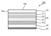
- FIG. 1 is a schematic cross-sectional view of an optical member according to one embodiment of the present invention.
- the optical member 100 of the illustrated example has a light guide plate 10 and a reflector 30 attached to the light guide plate 10 via a double-sided adhesive film 20.
- the double-sided pressure-sensitive adhesive film 20 has a first pressure-sensitive adhesive layer 21, a low-refractive index layer 22, and a second pressure-sensitive adhesive layer 23 from the light guide plate 10 side.
- the base material 24 is provided between the low refractive index layer 22 and the second pressure-sensitive adhesive layer 23.
- the low refractive index layer 22 is formed on the surface of the base material 24, and the first pressure-sensitive adhesive layer 21 and the second pressure-sensitive adhesive layer 23 are formed on both sides of the laminate of the base material 24 and the low-refractive index layer 22. Can be placed.
- the surface treatment layer 40 is formed on the side opposite to the double-sided adhesive film 20 of the reflector 30.
- the light guide plate 10 has an end surface 10a on which the light from the light source is incident and an exit surface 10b on which the incident light is emitted. That is, the light guide plate 10 is typically an edge light system in which light is incident from the end face 10a. More specifically, the light guide plate 10 guides the light incident on the end face 10a from the light source to the end side facing the end face 10a while receiving an internal reflection action or the like, and gradually emits the light in the light guide process. Emit from surface 10b. An emission pattern is typically provided on the emission surface 10b. Examples of the emission pattern include a concave-convex shape. Further, a light extraction pattern is typically provided on the surface of the light guide plate opposite to the exit surface. Examples of the light extraction pattern include white dots.
- any suitable light guide plate can be used.
- any suitable material can be used as long as the light emitted from the light source can be efficiently guided.
- the material constituting the light guide plate include acrylic resin such as polymethylmethacrylate (PMMA), polycarbonate (PC) resin, polyethylene terephthalate (PET) resin, styrene resin, and glass.
- the reflector may be a specular reflector or a diffuse reflector.
- the reflective plate include vapor deposition of aluminum, silver, etc. on a base material such as a highly reflective resin sheet (for example, acrylic plate), a thin metal plate such as aluminum or stainless steel, or a metal foil or a resin film such as polyester. Examples thereof include a sheet, a laminate of a base material such as a resin film such as polyester and a metal foil such as aluminum, and a resin film having pores (voids) formed inside.
- the double-sided adhesive film and the surface treatment layer constituting the optical member will be described in detail. Since the light guide plate and the reflector may have a structure well known in the industry, the description other than the above will be omitted.
- the double-sided adhesive film has a first adhesive layer 21, a low refractive index layer 22, and practically a base material 24 and a second adhesive from the light guide plate 10 side. It has an agent layer 23.
- the porosity of the low refractive index layer 22 is, for example, 40% by volume or more.
- Storage modulus at 23 ° C. of the first pressure-sensitive adhesive layer is, for example, 1.0 ⁇ 10 5 (Pa) ⁇ 1.0 ⁇ 10 7 (Pa), the storage modulus at 23 ° C. of the second pressure-sensitive adhesive layer is, for example, 1.0 ⁇ 10 5 (Pa) or less.
- the ratio of the thickness of the low refractive index layer to the total thickness of the pressure-sensitive adhesive layers present in the double-sided pressure-sensitive adhesive film is, for example, 0.10% to 5.00%, preferably 0.11% to 4 It is .50%, more preferably 0.12% to 4.00%.
- the thickness ratio is in such a range, damage to the low refractive index layer due to vibration can be further suppressed. More specifically, in in-vehicle applications and / or amusement applications, where large vibrations are present not only in the vertical direction but also in the horizontal direction, it is possible to satisfactorily suppress damage to the low refractive index layer, which is inferior in strength in the horizontal direction. can.
- the base material may typically be composed of a film or plate of resin (preferably a transparent resin).
- resins include thermoplastic resins and reactive resins (for example, ionizing radiation curable resins).
- thermoplastic resin include (meth) acrylic resins such as polymethyl methacrylate (PMMA) and polyacrylonitrile, polycarbonate (PC) resins, polyester resins such as PET, and cellulose-based resins such as triacetyl cellulose (TAC). Examples thereof include resins, cyclic polyolefin resins, and styrene resins.
- the ionizing radiation curable resin include epoxy acrylate resins and urethane acrylate resins. These resins may be used alone or in combination of two or more.
- the thickness of the base material is, for example, 10 ⁇ m to 100 ⁇ m, preferably 10 ⁇ m to 50 ⁇ m.
- the refractive index of the base material is preferably 1.47 or more, more preferably 1.47 to 1.60, and further preferably 1.47 to 1.55. Within such a range, the light can be guided to the image display cell without adversely affecting the light extracted from the light guide plate.
- the low refractive index layer typically has voids inside.
- the porosity of the low refractive index layer is 40% by volume or more, typically 50% by volume or more, preferably 70% by volume or more, and more preferably 80% by volume or more.
- the porosity is, for example, 90% by volume or less, preferably 85% by volume or less.
- the porosity is a value obtained by calculating the porosity from the value of the refractive index measured by an ellipsometer from Lorentz-Lorenz's formula (Lorentz-Lorenz's formula).
- the refractive index of the low refractive index layer is preferably 1.30 or less, more preferably 1.20 or less, and further preferably 1.15 or less.
- the lower limit of the refractive index can be, for example, 1.01. Within such a range, it is possible to realize extremely excellent light utilization efficiency in the laminated structure of the light guide plate and the peripheral member obtained via the optical laminate with the double-sided adhesive layer.
- Refractive index refers to the refractive index measured at a wavelength of 550 nm unless otherwise specified.
- the refractive index is a value measured by the method described in [Production Example 4] in the following examples.
- the low refractive index layer can be preferably formed by coating, printing, or the like.
- the material constituting the low refractive index layer for example, the materials described in International Publication No. 2004/1193966, JP2013-254183A, and JP2012-189802 can be adopted.
- silica-based compounds for example, silica-based compounds; hydrolyzable silanes and their partial hydrolysates and dehydration condensates; organic polymers; silicon compounds containing silanol groups; silicates in contact with acids and ion exchange resins.
- Active silica obtained by allowing the mixture; polymerizable monomers (eg, (meth) acrylic monomers, and styrene monomers); curable resins (eg, (meth) acrylic resins, fluorine-containing resins, and urethane resins); These combinations can be mentioned.
- the low index of refraction layer can be formed by coating or printing a solution or dispersion of such a material.
- the size of the void (hole) in the low refractive index layer shall indicate the diameter of the major axis of the diameter of the major axis and the diameter of the minor axis of the void (hole).
- the size of the voids (pores) is, for example, 2 nm to 500 nm.
- the size of the voids (pores) is, for example, 2 nm or more, preferably 5 nm or more, more preferably 10 nm or more, and further preferably 20 nm or more.
- the size of the void (pore) is, for example, 500 nm or less, preferably 200 nm or less, and more preferably 100 nm or less.
- the size range of the voids (pores) is, for example, 2 nm to 500 nm, preferably 5 nm to 500 nm, more preferably 10 nm to 200 nm, and even more preferably 20 nm to 100 nm.
- the size of the void (hole) can be adjusted to a desired size according to the purpose, application, and the like.
- the size of the voids (pores) can be quantified by the BET test method.
- the size of the void (hole) can be quantified by the BET test method. Specifically, 0.1 g of a sample (formed void layer) was put into the capillary of a specific surface area measuring device (manufactured by Micromeritic Co., Ltd .: ASAP2020), and then dried under reduced pressure at room temperature for 24 hours to allow voids. Degas the gas in the structure. Then, by adsorbing nitrogen gas on the sample, an adsorption isotherm is drawn and the pore distribution is obtained. Thereby, the void size can be evaluated.
- a specific surface area measuring device manufactured by Micromeritic Co., Ltd .: ASAP2020
- the haze of the low refractive index layer is, for example, less than 5%, preferably less than 3%.
- the haze is, for example, 0.1% or more, preferably 0.2% or more.
- the range of haze is, for example, 0.1% or more and less than 5%, preferably 0.2% or more and less than 3%.
- the haze can be measured by, for example, the following method.
- Haze is an index of transparency of the low refractive index layer.
- the void layer (low refractive index layer) is cut into a size of 50 mm ⁇ 50 mm and set in a haze meter (manufactured by Murakami Color Technology Research Institute: HM-150) to measure haze.
- the haze value is calculated from the following formula.
- Haze (%) [Diffusion transmittance (%) / Total light transmittance (%)] x 100 (%)
- Examples of the low refractive index layer having voids inside include a porous layer and / or a low refractive index layer having at least a part of an air layer.
- the porous layer typically includes airgel and / or particles (eg, hollow microparticles and / or porous particles).
- the low refractive index layer preferably a nanoporous layer (specifically, a porous layer within a diameter of more than 90% of the micropores of 10 -1 nm ⁇ 10 3 nm) .
- the particles are typically composed of silica-based compounds.
- the shape of the particles includes, for example, a spherical shape, a plate shape, a needle shape, a string shape, and a tuft of grapes.
- the string-shaped particles include, for example, particles in which a plurality of particles having a spherical, plate-like, or needle-like shape are connected in a bead shape, and short fibrous particles (for example, Japanese Patent Application Laid-Open No. 2001-188104). Short fibrous particles), and combinations thereof.
- the string-shaped particles may be linear or branched.
- Examples of the tufted particles of grape include those in which a plurality of spherical, plate-shaped, and needle-shaped particles are aggregated to form a tuft of grape.
- the shape of the particles can be confirmed, for example, by observing with a transmission electron microscope.
- the thickness of the low refractive index layer is preferably 0.2 ⁇ m to 5 ⁇ m, and more preferably 0.3 ⁇ m to 3 ⁇ m.
- the thickness of the low refractive index layer is within such a range, the damage prevention effect according to the present invention becomes remarkable. Further, the desired thickness ratio can be easily realized.
- the low refractive index layer can be typically formed by coating or printing as described above. With such a configuration, the low refractive index layer can be continuously provided by roll-to-roll.
- the low refractive index layer may be formed on the entire surface of the base material, or may be formed in a predetermined pattern.
- the coating is performed, for example, through a mask having a predetermined pattern. Any suitable method can be adopted for printing.
- the printing method may be a plate-type printing method such as gravure printing, offset printing, flexographic printing, or a plateless printing method such as inkjet printing, laser printing, or electrostatic printing. good.
- the low refractive index layer of the present embodiment is composed of one or a plurality of types of structural units that form a fine void structure, and the structural units are chemically bonded to each other via catalytic action.
- Examples of the shape of the structural unit include a particle shape, a fibrous shape, a rod shape, and a flat plate shape.
- the structural unit may have only one shape, or may have a combination of two or more shapes. In the following, a case where the low refractive index layer is a porous void layer in which the fine pore particles are chemically bonded to each other will be mainly described.
- Such a void layer can be formed, for example, by chemically bonding fine pore particles to each other in the void layer forming step.
- the shape of the "particle" (for example, the fine pore particles) is not particularly limited, and may be spherical or another shape, for example.
- the fine pore particles may be, for example, sol-gel beaded particles, nanoparticles (hollow nanosilica / nanoballoon particles), nanofibers and the like.
- the micropore particles typically contain an inorganic substance. Specific examples of the inorganic substance include silicon (Si), magnesium (Mg), aluminum (Al), titanium (Ti), zinc (Zn), and zirconium (Zr).
- the microporous particles are, for example, microporous particles of a silicon compound
- the porous body is, for example, a silicone porous body.
- the fine-pore particles of the silicon compound include, for example, a pulverized body of a gel-like silica compound.
- the low refractive index layer having a porous layer and / or an air layer at least in a part for example, it is made of a fibrous substance such as nanofibers, and the fibrous substances are entangled to form voids. There is a layered void layer.
- the method for producing such a void layer is not particularly limited, and is the same as, for example, in the case of a porous void layer in which the fine-pore particles are chemically bonded to each other.
- Still another form includes a void layer using hollow nanoparticles and nanoclay, and a void layer formed by using hollow nanoballoons and magnesium fluoride.
- the void layer may be a void layer composed of a single constituent substance, or may be a void layer composed of a plurality of constituent substances.
- the void layer may be composed of the single above-mentioned form, or may be composed of a plurality of the above-mentioned forms.
- the porous structure of the porous body can be, for example, a continuous foam structure having a continuous pore structure.
- the continuous foam structure means that, for example, in the above-mentioned silicone porous body, the pore structures are three-dimensionally connected, and it can be said that the internal voids of the pore structure are continuous. Since the porous body has a continuous foam structure, it is possible to increase the porosity. However, when single-foam particles such as hollow silica (particles having individual pore structures) are used, a continuous-foam structure cannot be formed.
- the coating film (crushed product of gel-like silicon compound) is included because the particles have a three-dimensional dendritic structure.
- the dendritic particles settle and deposit in the sol coating film), so that a continuous foam structure can be easily formed.
- the low index of refraction layer more preferably has a monolithic structure in which the continuous foam structure includes a plurality of pore distributions.
- the monolith structure means, for example, a hierarchical structure including a structure in which nano-sized fine voids are present and a continuous bubble structure in which the nano-voids are aggregated.
- a monolith structure for example, it is possible to impart both film strength and high porosity by imparting a high porosity with coarse continuous bubble voids while imparting film strength with fine voids.
- Such a monolith structure can be preferably formed by controlling the pore distribution of the void structure formed in the gel (gel-like silicon compound) in the pre-stage of pulverization into silica sol particles. Further, for example, when pulverizing a gel-like silicon compound, a monolith structure can be formed by controlling the particle size distribution of the pulverized silica sol particles to a desired size.
- the low refractive index layer contains, for example, a pulverized product of a gel-like compound as described above, and the pulverized products are chemically bonded to each other.
- the form of the chemical bond (chemical bond) between the ground products in the low refractive index layer is not particularly limited, and examples thereof include a cross-linking bond, a covalent bond, and a hydrogen bond.
- the gel form of the gel-like compound is not particularly limited. "Gel” generally refers to a solidified state in which solutes have an aggregated structure that loses independent motility due to interaction.
- the gel-like compound may be, for example, a wet gel or a xerogel.
- a wet gel includes a dispersion medium and the solute has a uniform structure in the dispersion medium
- a xerogel refers to a gel in which the solvent is removed and the solute has a network structure having voids. ..
- the gel-like compound examples include a gelled product obtained by gelling a monomer compound.
- a gelled product in which the silicon compounds of the monomers are bonded to each other examples include a gelled product in which the silicon compounds of the monomers are covalently bonded, hydrogen-bonded or intermolecularly bonded to each other.
- the covalent bond examples include a bond by dehydration condensation.
- the volume average particle size of the pulverized product in the low refractive index layer is, for example, 0.10 ⁇ m or more, preferably 0.20 ⁇ m or more, and more preferably 0.40 ⁇ m or more.
- the volume average particle size is, for example, 2.00 ⁇ m or less, preferably 1.50 ⁇ m or less, and more preferably 1.00 ⁇ m or less.
- the range of the volume average particle size is, for example, 0.10 ⁇ m to 2.00 ⁇ m, preferably 0.20 ⁇ m to 1.50 ⁇ m, and more preferably 0.40 ⁇ m to 1.00 ⁇ m.
- the particle size distribution can be measured by, for example, a particle size distribution evaluation device such as a dynamic light scattering method or a laser diffraction method, or an electron microscope such as a scanning electron microscope (SEM) or a transmission electron microscope (TEM).
- a particle size distribution evaluation device such as a dynamic light scattering method or a laser diffraction method
- an electron microscope such as a scanning electron microscope (SEM) or a transmission electron microscope (TEM).
- SEM scanning electron microscope
- TEM transmission electron microscope
- the type of gel compound is not particularly limited.
- examples of the gel-like compound include a gel-like silicon compound.
- the case where the gel-like compound is a gel-like silicon compound will be described as an example, but the present invention is not limited thereto.
- the crosslinked bond is, for example, a siloxane bond.
- the siloxane bond include a T2 bond, a T3 bond, and a T4 bond as shown below.
- the void layer low refractive index layer
- the void layer has a siloxane bond, it may have any one kind of bond, any two kinds of bonds, or all three kinds of bonds. May be good.
- the larger the ratio of T2 and T3 in the siloxane bond the more flexible it is, and the original characteristics of the gel can be expected.
- the larger the ratio of T4 the easier it is for the film strength to develop. Therefore, it is preferable to change the ratio of T2, T3 and T4 according to the purpose, application, desired characteristics and the like.
- the contained silicon atoms are siloxane bonded.
- the proportion of unbonded silicon atoms (that is, residual silanol) in the total silicon atoms contained in the void layer is, for example, less than 50%, preferably 30% or less, and more preferably 15%. It is as follows.
- the monomer silicon compound is not particularly limited.
- the monomer silicon compound include a compound represented by the following formula (1).
- the gel-like silicon compound is a gelled product in which the silicon compounds of the monomers are hydrogen-bonded or intermolecularly bonded to each other as described above, the monomers of the formula (1) are hydrogen-bonded via, for example, their respective hydroxyl groups. can.
- X is, for example, 2, 3 or 4, preferably 3 or 4.
- R 1 is, for example, a linear or branched alkyl group.
- the carbon number of R 1 is, for example, 1 to 6, preferably 1 to 4, and more preferably 1 to 2.
- Examples of the linear alkyl group include a methyl group, an ethyl group, a propyl group, a butyl group, a pentyl group, a hexyl group and the like, and examples of the branched alkyl group include an isopropyl group and an isobutyl group.
- the silicon compound represented by the formula (1) include a compound represented by the following formula (1') in which X is 3.
- R 1 is the same as in the case of the formula (1), and is, for example, a methyl group.
- the silicon compound is tris (hydroxy) methyl silane.
- X is 3, the silicon compound is, for example, a trifunctional silane having three functional groups.
- silicon compound represented by the formula (1) is a compound in which X is 4.
- the silicon compound is, for example, a tetrafunctional silane having four functional groups.
- the silicon compound of the monomer may be, for example, a hydrolyzate of a silicon compound precursor.
- the silicon compound precursor may be, for example, a compound capable of producing a silicon compound by hydrolysis, and specific examples thereof include a compound represented by the following formula (2).
- R 1 and R 2 are independently linear or branched alkyl groups, respectively. R 1 and R 2 may be the same or different R 1 may be the same or different from each other when X is 2. R 2 may be the same or different from each other.
- X and R 1 are, for example, the same as X and R 1 in the formula (1).
- R 2 for example, the example of R 1 in the formula (1) can be incorporated.
- the silicon compound precursor represented by the formula (2) include a compound represented by the following formula (2') in which X is 3.
- R 1 and R 2 are the same as in the case of the formula (2), respectively.
- the silicon compound precursor is trimethoxy (methyl) silane (hereinafter, also referred to as “MTMS”).
- the monomer silicon compound for example, trifunctional silane is preferable because it is excellent in low refractive index.
- the silicon compound of the monomer is preferably a tetrafunctional silane, for example, from the viewpoint of being excellent in strength (for example, scratch resistance).
- the silicon compound of the monomer may contain only trifunctional silane, may contain only tetrafunctional silane, may contain both trifunctional silane and tetrafunctional silane, and may further contain other silicon compounds. But it may be.
- the ratio is not particularly limited and can be appropriately set.
- the method is typically a precursor forming step of forming a void structure which is a precursor of a low refractive index layer (void layer) on a resin film, and a cross-linking reaction inside the precursor after the precursor forming step. Includes a cross-linking reaction step, which causes
- the method includes a step of preparing a containing liquid for producing a containing liquid containing fine pore particles (hereinafter, may be referred to as a “micropore particle-containing liquid” or simply a “containing liquid”), and a drying method for drying the containing liquid. Further including a step, in the precursor forming step, the fine pore particles in the dried body are chemically bonded to each other to form a precursor.
- the containing liquid is not particularly limited, and is, for example, a suspension containing fine pore particles.
- the fine pore particles are a pulverized product of a gel-like compound and the void layer is a porous body containing the pulverized product of the gel-like compound (preferably a silicone porous body) will be described.
- the low refractive index layer can be similarly formed when the fine pore particles are other than the pulverized product of the gel-like compound.
- a low refractive index layer (void layer) having a very low refractive index is formed.
- the reason is presumed as follows, for example.
- the speculation does not limit the method of forming the low refractive index layer.
- the crushed product is a crushed gel-like silicon compound
- the three-dimensional structure of the gel-like silicon compound before crushing is dispersed in the three-dimensional basic structure.
- a crushed product of a gel-like silicon compound is applied onto a resin film to form a precursor having a porous structure based on a three-dimensional basic structure. That is, according to the above method, a new porous structure (three-dimensional basic structure) is formed by coating the pulverized material, which is different from the three-dimensional structure of the gel-like silicon compound. Therefore, in the finally obtained void layer, it is possible to realize a low refractive index that functions as much as, for example, an air layer. Further, in the above method, the three-dimensional basic structure is fixed because the crushed substances are chemically bonded to each other. Therefore, the finally obtained void layer can maintain sufficient strength and flexibility even though it has a structure having voids.
- the precursor forming step and the crosslinking reaction step are performed as separate steps.
- the cross-linking reaction step is preferably carried out in multiple steps.
- the strength of the precursor can be further improved as compared with the case where the cross-linking reaction step is carried out in one step, and a low refractive index layer having both high void ratio and strength can be obtained.
- This mechanism is unknown, but it is speculated as follows, for example. That is, as described above, if the film strength is improved by a catalyst or the like at the same time as the formation of the void layer, there is a problem that the film strength is improved but the porosity is decreased due to the progress of the catalytic reaction.
- the precursor forming step for example, particles having a certain shape are laminated to form a precursor of a void layer.
- the strength of the precursor at this point is very weak.
- a product capable of chemically bonding fine pore particles for example, a strong base catalyst generated from a photobase generator
- a light or thermoactive catalytic reaction one step of the cross-linking reaction step. eye. It is considered that by further heating aging (the second step of the cross-linking reaction step) in order to proceed the reaction efficiently and in a short time, the chemical bonding (cross-linking reaction) between the fine-pore particles further progresses and the strength is improved.
- the fine pore particles are fine pore particles of a silicon compound (for example, a pulverized product of a gel-like silica compound) and a residual silanol group (Si—OH group) is present in the precursor, the residual silanol groups are crosslinked. It is considered that they are chemically bound by the reaction.
- this explanation is also an example, and does not limit the method of forming the low refractive index layer.
- the above method has a content liquid preparation step of producing a content liquid containing fine pore particles.
- the fine pore particles are pulverized products of a gel-like compound
- the pulverized product is obtained by, for example, pulverizing a gel-like compound.
- the pulverization of the gel-like compound destroys the three-dimensional structure of the gel-like compound and disperses it into the three-dimensional basic structure.
- An example of preparation of the pulverized product is as follows.
- Gelation of the monomer compound can be performed, for example, by hydrogen-bonding the monomer compounds to each other or intermolecular force bonding.
- the monomer compound include a silicon compound represented by the above formula (1). Since the silicon compound of the formula (1) has a hydroxyl group, hydrogen bonds or intermolecular force bonds can be formed between the monomers of the formula (1), for example, via the respective hydroxyl groups.
- the silicon compound may be a hydrolyzate of the silicon compound precursor, and may be produced, for example, by hydrolyzing the silicon compound precursor represented by the above formula (2).
- the method of hydrolyzing the monomer compound precursor is not particularly limited, and can be carried out, for example, by a chemical reaction in the presence of a catalyst.
- the catalyst include acids such as oxalic acid and acetic acid.
- the hydrolysis reaction is carried out, for example, by slowly mixing an aqueous solution of oxalic acid with a mixed solution (for example, suspension) of a silicon compound and dimethyl sulfoxide in a room temperature environment, and then stirring the mixture as it is for about 30 minutes. be able to.
- a mixed solution for example, suspension
- subsequent gelation, aging, and heating / immobilization after formation of a void structure can be performed more efficiently. It can be carried out.
- the gelation of the monomer compound can be performed, for example, by a dehydration condensation reaction between the monomers.
- the dehydration condensation reaction is preferably carried out, for example, in the presence of a catalyst, and examples of the catalyst include acid catalysts such as hydrochloric acid, oxalic acid and sulfuric acid, and bases such as ammonia, potassium hydroxide, sodium hydroxide and ammonium hydroxide. Examples thereof include a dehydration condensation catalyst such as a catalyst.
- a base catalyst is preferable.
- the amount of the catalyst added to the monomer compound is not particularly limited.
- the catalyst can be added, for example, to 1 mol of the monomer compound, preferably from 0.1 mol to 10 mol, more preferably from 0.05 mol to 7 mol, still more preferably from 0.1 mol to 5 mol.
- the gelation of the monomer compound is preferably performed in a solvent, for example.
- the ratio of the monomer compound to the solvent is not particularly limited.
- the solvent include dimethyl sulfoxide (DMSO), N-methylpyrrolidone (NMP), N, N-dimethylacetamide (DMAc), dimethylformamide (DMF), ⁇ -butyllactone (GBL), acetonitrile (MeCN), and ethylene. Glycolethyl ether (EGEE) and the like can be mentioned.
- the solvent may be used alone or in combination of two or more.
- the solvent used for gelation is also hereinafter referred to as "gelling solvent".
- the conditions for gelation are not particularly limited.
- the treatment temperature for the solvent containing the monomer compound is, for example, 20 ° C. to 30 ° C., preferably 22 ° C. to 28 ° C., and more preferably 24 ° C. to 26 ° C.
- the treatment time is, for example, 1 minute to 60 minutes, preferably 5 minutes to 40 minutes, and more preferably 10 minutes to 30 minutes.
- the treatment conditions are not particularly limited, and these examples can be incorporated.
- the gel-like compound obtained by gelation is preferably subjected to a aging treatment after the gelation reaction.
- a aging treatment for example, it is possible to further grow the primary particles of the gel having the three-dimensional structure obtained by gelation and increase the size of the particles themselves, and as a result, the particles come into contact with each other.
- the contact state of the neck portion can be changed from point contact to surface contact (increasing the contact area).
- the strength of the gel itself is increased, and as a result, the strength of the three-dimensional basic structure after pulverization can be improved.
- the drying step after coating the pulverized product it is possible to prevent the pore size of the void structure in which the three-dimensional basic structure is deposited from shrinking due to the volatilization of the solvent in the drying process.
- the aging treatment can be performed, for example, by incubating the gel compound at a predetermined temperature for a predetermined time.
- the aging temperature is, for example, 30 ° C. or higher, preferably 35 ° C. or higher, and more preferably 40 ° C. or higher.
- the aging temperature is, for example, 80 ° C. or lower, preferably 75 ° C. or lower, and more preferably 70 ° C. or lower.
- the aging temperature range is, for example, 30 ° C. to 80 ° C., preferably 35 ° C. to 75 ° C., and more preferably 40 ° C. to 70 ° C.
- the aging time is, for example, 5 hours or more, preferably 10 hours or more, and more preferably 15 hours or more.
- the aging time is, for example, 50 hours or less, preferably 40 hours or less, and more preferably 30 hours or less.
- the range of aging time is, for example, 5 hours to 50 hours, preferably 10 hours to 40 hours, and more preferably 15 hours to 30 hours.
- the aging conditions can be optimized so as to obtain, for example, an increase in the silica primary particle size and an increase in the contact area of the neck portion. Furthermore, it is preferable to consider the boiling point of the solvent used.
- the aging temperature is too high, the solvent will volatilize excessively, and the concentration of the coating liquid (gel liquid) will increase the three-dimensional void structure. There is a possibility that problems such as closing of the pores of the solvent may occur.
- the aging temperature is too low, not only the effect of aging cannot be sufficiently obtained, but also the temperature variation over time in the mass production process increases, so that a low refractive index layer having inferior characteristics can be formed. There is sex.
- the same solvent as the gelling treatment can be used.
- the reaction product after the gel treatment that is, the solvent containing the gel-like compound
- the reaction product after the gel treatment is directly subjected to the aging treatment.
- the number of moles of residual silanol groups contained in the gel (gel-like compound, for example, gel-like silicon compound) that has been aged after gelation is, for example, 50% or less, preferably 40% or less, more preferably. Is less than 30%.
- the number of moles of the residual silanol group is, for example, 1% or more, preferably 3% or more, and more preferably 5% or more.
- the range of the number of moles of the residual silanol group is, for example, 1% to 50%, preferably 3% to 40%, and more preferably 5% to 30%.
- the lower the number of moles of residual silanol groups the more preferable. If the number of moles of silanol groups is too high, for example, the void structure may not be retained by the time the precursor of the silicone porous body is crosslinked. On the other hand, if the number of moles of silanol groups is too low, for example, in the step of preparing a fine pore particle-containing liquid (for example, suspension) and / or the subsequent steps, the pulverized product of the gel compound cannot be crosslinked, which is sufficient.
- the number of moles of the residual silanol group is, for example, the ratio of the residual silanol groups when the number of moles of the alkoxy group of the raw material (for example, the monomer compound precursor) is 100.
- the above is an example of a silanol group.
- a silicon compound of a monomer is modified with various reactive functional groups, the same items and conditions can be applied to each functional group.
- the obtained gel-like compound is pulverized.
- the gel-like compound in the gelling solvent may be subjected to the pulverization treatment as it is, or the gel-like compound in the other solvent may be replaced with another solvent.
- the compound may be subjected to a pulverization treatment.
- the catalyst used in the gelation reaction and the solvent used remain after the aging step to cause gelation of the liquid with time (pot life) and a decrease in drying efficiency during the drying step, other cases may occur. It is preferable to replace it with a solvent.
- the other solvent is also hereinafter referred to as a "solvent for pulverization".
- the solvent for crushing is not particularly limited, and for example, an organic solvent can be used.
- the organic solvent include solvents having a boiling point of, for example, 130 ° C. or lower, preferably 100 ° C. or lower, and more preferably 85 ° C. or lower. Specific examples include isopropyl alcohol (IPA), ethanol, methanol, butanol, propylene glycol monomethyl ether (PGME), methyl cellosolve, acetone, dimethylhomamide (DMF), isobutyl alcohol and the like.
- the pulverizing solvent may be used alone or in combination of two or more.
- the combination of the gelling solvent and the pulverizing solvent is not particularly limited, and examples thereof include a combination of DMSO and IPA, DMSO and ethanol, DMSO and methanol, DMSO and butanol, and DMSO and isobutyl alcohol.
- the method for crushing the gel-like compound is not particularly limited, and can be carried out by, for example, an ultrasonic homogenizer, a high-speed rotation homogenizer, or another crushing device using a cavitation phenomenon.
- a device that crushes media such as a ball mill physically destroys the void structure of the gel during crushing, whereas a cavitation crusher such as a homogenizer has a three-dimensional gel structure because it is a medialess method, for example.
- the already contained silica particle bonding surface with a relatively weak bond is peeled off by a high-speed shearing force.
- the resulting gel three-dimensional structure can, for example, maintain a void structure having a particle size distribution in a certain range, and can reshape the void structure due to deposition during coating and drying.
- the pulverization conditions are not particularly limited, and it is preferable that the gel can be pulverized without volatilizing the solvent, for example, by giving an instantaneous high-speed flow.
- the amount of work such as crushing time and strength is insufficient, for example, coarse grains may remain and dense pores may not be formed, and appearance defects may increase and high quality may not be obtained.
- the amount of work is excessive, for example, the particles become finer than the desired particle size distribution, the size of the voids deposited after coating and drying becomes fine, and the desired porosity may not be obtained.
- a liquid (for example, suspension) containing fine pore particles crushed product of gel-like compound
- a liquid containing the fine pore particles and the catalyst can be prepared by adding a catalyst that chemically bonds the fine pore particles to each other after the liquid containing the fine pore particles is prepared or during the preparation step. ..
- the catalyst may be, for example, a catalyst that promotes cross-linking between fine-pore particles.
- the chemical reaction for chemically bonding the fine pore particles to each other it is preferable to use the dehydration condensation reaction of the residual silanol group contained in the silica sol molecule.
- the catalyst include a photoactive catalyst and a thermoactive catalyst.
- the photoactive catalyst for example, in the precursor forming step, the fine pore particles can be chemically bonded (for example, crosslinked) to each other without heating. According to this, for example, in the precursor forming step, shrinkage of the entire precursor is unlikely to occur, so that a higher porosity can be maintained.
- a substance that generates a catalyst may be used in addition to or instead of the catalyst.
- a substance that generates a catalyst by light may be used in addition to or instead of a photoactive catalyst, or a catalyst is generated by heat in addition to or in place of a thermoactive catalyst.
- a substance heat catalyst generator
- the photocatalyst generator include a photobase generator (a substance that generates a basic catalyst by light irradiation), a photoacid generator (a substance that generates an acidic catalyst by light irradiation), and the like. preferable.
- the photobase generator include 9-anthrylmethyl N, N-diethylcarbamate (trade name WPBG-018), (E) -1- [3- (2-hydroxy).
- Phenyl) -2-propenoyl] piperidine ((E) -1- [3- (2-hydroxyphenyl) -2-propenoyl] piperidine, trade name WPBG-027), 1- (anthraquinone-2-yl) ethyl imidazole carboxylate (1- (anthraquinon-2-yl) ethyl imidazolecarboxylate, trade name WPBG-140), 2-nitrophenylmethyl 4-methacryloyloxypiperidin-1-carboxylate (trade name WPBG-165), 1,2-diisopropyl-3 -[Bis (dimethylamino) methylene] guanidium 2- (3-benzoylphenyl) propionate (trade name WPBG-266), 1,2-dicyclohexyl-4,4,5,5-tetramethylbiguanidium n-butyltri Phenylborate (trade name WPBG-300) and 2- (9-o
- the product names including the above "WPBG” are all product names of Wako Pure Chemical Industries, Ltd.
- the photoacid generator include aromatic sulfonium salt (trade name SP-170: ADEKA), triarylsulfonium salt (trade name CPI101A: San Apro), and aromatic iodonium salt (trade name Irgacure 250: Ciba Japan). ) Etc. can be mentioned.
- the catalyst for chemically bonding the fine pore particles is not limited to the photoactive catalyst and the photocatalyst generator, and may be, for example, a thermoactive catalyst or a thermocatalyst generator such as urea.
- the catalyst for chemically bonding the fine pore particles examples include a base catalyst such as potassium hydroxide, sodium hydroxide and ammonium hydroxide, and an acid catalyst such as hydrochloric acid, acetic acid and oxalic acid. Of these, a base catalyst is preferable.
- the catalyst or catalyst generator that chemically bonds the fine-pore particles to each other is used, for example, by adding it to a sol particle solution (for example, suspension) containing a pulverized product (fine-pore particles) immediately before coating. It can be used as a mixed solution in which a catalyst or a catalyst generator is mixed with a solvent.
- the mixed solution may be, for example, a coating solution which is directly added to the sol particle solution and dissolved, a solution in which a catalyst or a catalyst generator is dissolved in a solvent, or a dispersion solution in which a catalyst or a catalyst generator is dispersed in a solvent.
- the solvent is not particularly limited, and examples thereof include water and a buffer solution.
- a cross-linking auxiliary agent for indirectly binding the pulverized products of the gel may be added to the gel-containing liquid.
- the cross-linking auxiliary agent enters between the particles (the pulverized product), and the particles and the cross-linking auxiliary agent interact with each other or bond with each other, so that particles slightly separated from each other can also be bonded to each other. It is possible to increase the strength efficiently.
- the cross-linking auxiliary agent a multi-cross-linked silane monomer is preferable.
- the polycrosslinked silane monomer may have, for example, 2 or more and 3 or less alkoxysilyl groups, and the chain length between the alkoxysilyl groups may be 1 or more and 10 or less carbon atoms, and is an element other than carbon. May also be included.
- the cross-linking aid include bis (trimethoxysilyl) ethane, bis (triethoxysilyl) ethane, bis (trimethoxysilyl) methane, bis (triethoxysilyl) methane, bis (triethoxysilyl) propane, and bis.
- the amount of the cross-linking aid added is not particularly limited, but is, for example, 0.01 to 20% by weight, 0.05 to 15% by weight, or 0.1 to 10% by weight based on the weight of the pulverized silicon compound. By weight%.
- a liquid containing fine pore particles for example, suspension
- the coating for example, various coating methods described later can be used, and the coating is not limited thereto.
- a coating film containing fine pore particles and a catalyst can be formed by directly coating a liquid containing fine pore particles (for example, a pulverized product of a gel-like silica compound) on a substrate.
- the coating film can also be referred to as, for example, a coating layer.
- a new three-dimensional structure is constructed by sedimentation and deposition of crushed material in which the three-dimensional structure is destroyed.
- the containing liquid containing the fine pore particles may not contain a catalyst for chemically bonding the fine pore particles to each other.
- the coating film may be sprayed with a catalyst that chemically bonds the fine pore particles to each other, or the precursor forming step may be performed while spraying the catalyst.
- the containing liquid containing the fine pore particles contains a catalyst that chemically bonds the fine pore particles to each other, and the action of the catalyst contained in the coating film chemically bonds the fine pore particles to each other to form a porous body. May form a precursor of.
- the above solvent (hereinafter, also referred to as "coating solvent”) is not particularly limited, and for example, an organic solvent can be used.
- the organic solvent include solvents having a boiling point of 150 ° C. or lower. Specific examples include IPA, ethanol, methanol, n-butanol, 2-butanol, isobutyl alcohol, pentanol and the like, and the same solvent as the pulverizing solvent can be used.
- a pulverizing solvent containing a pulverized product of the gel-like compound may be used as it is in the step of forming the coating film. ..
- sol particle liquid a sol-like pulverized product
- the sol particle solution can be continuously formed into a void layer having a film strength of a certain level or higher by, for example, coating and drying on a substrate and then performing the chemical cross-linking.
- sol in the embodiment of the present invention means that by crushing the three-dimensional structure of a gel, silica sol particles having a nano-three-dimensional structure holding a part of the void structure are dispersed in a solvent to improve fluidity. The state shown.
- the concentration of the ground product in the coating solvent is not particularly limited, and is, for example, 0.3% (v / v) to 50% (v / v), preferably 0.5% (v / v) to 30. % (V / v), more preferably 1.0% (v / v) to 10% (v / v). If the concentration of the pulverized product is too high, for example, the fluidity of the sol particle solution is significantly reduced, which may cause agglomerates and coating streaks during coating. If the concentration of the pulverized product is too low, for example, not only does it take a considerable amount of time to dry the solvent of the sol particle solution, but also the residual solvent immediately after drying becomes high, so that the porosity may decrease. ..
- the physical characteristics of the sol are not particularly limited.
- the shear viscosity of the sol is, for example, 100 cPa ⁇ s or less, preferably 10 cPa ⁇ s or less, and more preferably 1 cPa ⁇ s or less at a shear rate of 10001 / s. If the shear viscosity is too high, for example, coating streaks may occur, and problems such as a decrease in the transfer rate of gravure coating may be observed. On the contrary, if the shear viscosity is too low, for example, the wet coating thickness at the time of coating cannot be increased, and a desired thickness may not be obtained after drying.
- the amount of the pulverized product applied to the base material is not particularly limited, and can be appropriately set according to, for example, the thickness of the desired silicone porous body (as a result, the low refractive index layer).
- the amount of the pulverized product applied to the base material is, for example, 0.01 ⁇ g to 60,000 ⁇ g per 1 m 2 of the base material area, preferably 0. .1 ⁇ g to 5000 ⁇ g, more preferably 1 ⁇ g to 50 ⁇ g.
- the preferable amount of sol particle liquid to be applied because it is related to, for example, the concentration of the liquid and the coating method, but considering productivity, it is possible to apply as thin a layer as possible. preferable. If the amount of coating is too large, for example, there is a high possibility that the solvent will be dried in a drying oven before it volatilizes. As a result, the nano-crushed sol particles settle and deposit in the solvent, and the solvent dries before forming the void structure, which may inhibit the formation of the voids and greatly reduce the porosity. On the other hand, if the amount of coating is too thin, there is a possibility that the risk of coating repelling may increase due to unevenness of the base material, variation in hydrophobicity, and the like.
- the method for forming the low refractive index layer includes, for example, as described above, a precursor forming step of forming a void structure which is a precursor of the void layer (low refractive index layer) on the base material.
- the precursor forming step is not particularly limited, and for example, a precursor (void structure) may be formed by a drying step of drying a coating film produced by applying a fine pore particle-containing liquid.
- a drying treatment in the drying step for example, not only the solvent (solvent contained in the sol particle solution) in the above coating film is removed, but also the sol particles are settled and deposited during the drying treatment to form a void structure. can do.
- the temperature of the drying treatment is, for example, 50 ° C.
- the drying treatment time is, for example, 0.1 minutes to 30 minutes, preferably 0.2 minutes to 10 minutes, and more preferably 0.3 minutes to 3 minutes.
- the drying treatment temperature and time are preferably lower and shorter, for example, in relation to continuous productivity and the development of high porosity. If the conditions are too strict, for example, when coating a resin film, the resin film will stretch in the drying oven as it approaches the glass transition temperature of the resin film, and the void structure formed immediately after coating. There is a possibility that defects such as cracks may occur. On the other hand, if the conditions are too loose, for example, since the residual solvent is contained at the timing of leaving the drying oven, there is a possibility that appearance defects such as scratches may occur when rubbing against the roll in the next process. be.
- the drying treatment may be, for example, natural drying, heat drying, or vacuum drying. Above all, it is preferable to use heat drying on the premise of continuous industrial production.
- the method of heat drying is not particularly limited, and for example, general heating means can be used. Examples of the heating means include a hot air blower, a heating roll, a far-infrared heater, and the like.
- the solvent used a solvent having a low surface tension is preferable for the purpose of suppressing the generation of shrinkage stress due to the volatilization of the solvent during drying and the cracking phenomenon of the void layer (silicone porous body) due to the generation.
- the solvent examples include lower alcohols typified by isopropyl alcohol (IPA), hexane, perfluorohexane and the like. Further, a small amount of a perfluorosurfactant or a silicone-based surfactant may be added to the IPA or the like to reduce the surface tension.
- IPA isopropyl alcohol
- hexane hexane
- perfluorohexane perfluorohexane
- silicone-based surfactant may be added to the IPA or the like to reduce the surface tension.
- the method for forming the low refractive index layer includes a cross-linking reaction step of causing a cross-linking reaction inside the precursor after the precursor forming step, and in the cross-linking reaction step, a basic substance is subjected to light irradiation or heating.
- the cross-linking reaction step is multi-step.
- the micropore particles are chemically bonded to each other by the action of a catalyst (basic substance).
- a catalyst basic substance
- dehydration condensation of silanol groups and formation of siloxane bonds are induced by performing a high temperature treatment of 200 ° C. or higher.
- a high temperature treatment of 200 ° C. or higher.
- various additives that catalyze the dehydration condensation reaction for example, a relatively low drying temperature of about 100 ° C. and a number of the substrates (resin film) are not damaged.
- the void structure can be continuously formed and fixed in a short treatment time of less than a minute.
- the method of chemically bonding is not particularly limited, and can be appropriately determined, for example, depending on the type of gel-like silicon compound.
- the chemical bond can be carried out by, for example, a chemical cross-linking between the pulverized products, and in addition, for example, when inorganic particles such as titanium oxide are added to the pulverized product, the inorganic particles It is also conceivable to chemically cross-link the pulverized product with the pulverized product. Further, when a biocatalyst such as an enzyme is supported, a site different from the catalytically active site and the pulverized product may be chemically crosslinked.
- the low refractive index layer for example, not only the void layer (silicone porous body) formed between sol particles but also an organic-inorganic hybrid void layer, a host guest void layer, and the like can be considered.
- the stage at which the chemical reaction in the presence of the catalyst is performed (occurs) in the method for forming the low refractive index layer is not particularly limited, and is, for example, performed at at least one stage in the multi-step cross-linking reaction step.
- the drying step may also serve as the precursor forming step.
- a multi-step cross-linking reaction step may be performed, and at least one step thereof, the fine pore particles may be chemically bonded to each other by the action of a catalyst.
- the fine pore particles may be chemically bonded to each other by light irradiation to form a porous precursor.
- the catalyst is a thermally active catalyst, the fine pore particles may be chemically bonded to each other by heating to form a porous precursor in the crosslinking reaction step.
- a coating film containing a catalyst added to a sol particle solution (for example, a suspension) in advance is irradiated or heated with light, or the coating film is sprayed with a catalyst and then irradiated with light or heated. Alternatively, it can be carried out by irradiating light or heating while spraying a catalyst.
- the integrated light amount in light irradiation is not particularly limited, and is, for example, 200 mJ / cm 2 to 800 mJ / cm 2 , preferably 250 mJ / cm 2 to 600 mJ / cm 2 , and more preferably 300 mJ / cm in terms of wavelength of 360 nm. It is 2 to 400 mJ / cm 2 .
- an integrated light amount of 200 mJ / cm 2 or more is preferable. Further, from the viewpoint of preventing heat wrinkles from being generated due to damage to the base material under the void layer, an integrated light amount of 800 mJ / cm 2 or less is preferable.
- the conditions of heat treatment are not particularly limited.
- the heating temperature is, for example, 50 ° C. to 250 ° C., preferably 60 ° C. to 150 ° C., and more preferably 70 ° C. to 130 ° C.
- the heating time is, for example, 0.1 minutes to 30 minutes, preferably 0.2 minutes to 10 minutes, and more preferably 0.3 minutes to 3 minutes.
- the step of drying the sol particle liquid (for example, suspension) coated as described above may also serve as the step of performing a chemical reaction in the presence of a catalyst. That is, in the step of drying the coated sol particle liquid (for example, suspension), the pulverized products (micropore particles) may be chemically bonded to each other by a chemical reaction in the presence of a catalyst. In this case, the pulverized products (fine pore particles) may be more firmly bonded to each other by further heating the coating film after the drying step.
- the chemical reaction in the presence of the catalyst may also occur in the step of preparing the fine pore particle-containing liquid (for example, suspension) and the step of applying the fine pore particle-containing liquid.
- this speculation does not limit the method of forming the low refractive index layer.
- a solvent having a low surface tension is preferable for the purpose of suppressing the generation of shrinkage stress due to the volatilization of the solvent during drying and the cracking phenomenon of the void layer due to the generation.
- lower alcohols typified by isopropyl alcohol (IPA), hexane, perfluorohexane and the like can be mentioned.
- the strength of the void layer (low refractive index layer) can be further improved as compared with the case where the cross-linking reaction step is one step, for example, by having the cross-linking reaction step in multiple steps.
- the second and subsequent steps of the crosslinking reaction step may be referred to as an “aging step”.
- the cross-linking reaction may be further promoted inside the precursor by heating the precursor.
- the phenomenon and mechanism that occur in the cross-linking reaction step are unknown, but are as described above, for example.
- the strength can be improved by lowering the heating temperature to cause a cross-linking reaction while suppressing the shrinkage of the precursor, and both high porosity and strength can be achieved.
- the temperature in the aging step is, for example, 40 ° C. to 70 ° C., preferably 45 ° C. to 65 ° C., and more preferably 50 ° C. to 60 ° C.
- the time for performing the aging step is, for example, 10 hr to 30 hr, preferably 13 hr to 25 hr, and more preferably 15 hr to 20 hr.
- the low refractive index layer formed as described above has excellent strength, it can be, for example, a roll-shaped porous body, and has advantages such as good production efficiency and easy handling.
- the low refractive index layer (void layer) formed in this way may be laminated with another film (layer) to form a laminated structure including a porous structure.
- each component in the laminated structure may be laminated via, for example, an adhesive or an adhesive. Since the lamination of each component is efficient, for example, the lamination may be performed by continuous processing using a long film (so-called Roll to Roll, etc.), and when the base material is a molded product, an element, or the like, the lamination may be performed. Those that have undergone batch processing may be laminated.
- the first adhesive layer has a hardness such that the adhesive constituting the first adhesive layer does not penetrate into the voids of the low refractive index layer under normal conditions.
- Storage modulus at 23 ° C. of the first pressure-sensitive adhesive layer is as described above 1.0 ⁇ 10 5 (Pa) ⁇ 1.0 ⁇ 10 7 (Pa).
- the storage elastic modulus is based on the method described in JIS K7244-1 "Plastic-Test method for dynamic mechanical properties", and the temperature rise rate is 5 ° C. in the range of -50 ° C to 150 ° C under the condition of frequency 1 Hz. It is obtained by reading the value at 23 ° C. when measured in minutes.
- any suitable pressure-sensitive adhesive can be used as long as it has the above-mentioned characteristics.
- Typical examples of the pressure-sensitive adhesive include an acrylic pressure-sensitive adhesive (acrylic pressure-sensitive adhesive composition).
- the acrylic pressure-sensitive adhesive composition typically contains a (meth) acrylic polymer as a main component (base polymer).
- the (meth) acrylic polymer can be contained in the pressure-sensitive adhesive composition in a proportion of, for example, 50% by weight or more, preferably 70% by weight or more, and more preferably 90% by weight or more in the solid content of the pressure-sensitive adhesive composition.
- the (meth) acrylic polymer contains an alkyl (meth) acrylate as a main component as a monomer unit.
- (meth) acrylate means acrylate and / or methacrylate.
- alkyl group of the alkyl (meth) acrylate include a linear or branched-chain alkyl group having 1 to 18 carbon atoms. The average number of carbon atoms of the alkyl group is preferably 3 to 9.
- the monomers constituting the (meth) acrylic polymer include carboxyl group-containing monomers, hydroxyl group-containing monomers, amide group-containing monomers, aromatic ring-containing (meth) acrylates, and heterocyclic ring-containing (meth) monomers. Examples thereof include comonomer such as acrylate.
- the comonomer is preferably a hydroxyl group-containing monomer and / or a heterocyclic-containing (meth) acrylate, and more preferably N-acryloyl morpholine.
- the acrylic pressure-sensitive adhesive composition may preferably contain a silane coupling agent and / or a cross-linking agent.
- the silane coupling agent include an epoxy group-containing silane coupling agent.
- the cross-linking agent include isocyanate-based cross-linking agents and peroxide-based cross-linking agents. Details of such a pressure-sensitive adhesive layer or an acrylic pressure-sensitive adhesive composition are described in, for example, Japanese Patent No. 4140736, and the description in the patent gazette is incorporated herein by reference.
- the thickness of the first pressure-sensitive adhesive layer is preferably 3 ⁇ m to 30 ⁇ m, and more preferably 5 ⁇ m to 10 ⁇ m.
- the thickness of the first pressure-sensitive adhesive layer is within such a range, it has an advantage that the influence of the pressure-sensitive adhesive layer thickness on the total thickness is small while having sufficient adhesive force. Further, the desired thickness ratio can be easily realized.
- the second adhesive layer is applied to a device that vibrates continuously when used in a car or the like, and can absorb the transmission of the vibration to suppress damage to the low refractive index layer. It is composed of a pressure-sensitive adhesive having a softness. Storage modulus at 23 ° C.
- 1.0 ⁇ 10 5 (Pa) or less e.g., 1.0 ⁇ 10 5 (Pa) or less, 9.5 ⁇ 10 4 (Pa) or less, 9.0 ⁇ 10 4 (Pa) or less, 8.5 ⁇ 10 4 (Pa) or less, 8.0 ⁇ 10 4 (Pa) or less, 7.5 ⁇ 10 4 (Pa) or less, Or 7.0 ⁇ 10 4 (Pa) or less and 1.0 ⁇ 10 3 (Pa) or more, 5.0 ⁇ 10 3 (Pa) or more, 1.0 ⁇ 10 4 (Pa) or more, or 5 It is 0.0 ⁇ 10 4 (Pa) or more. It is preferably 5.0 ⁇ 10 3 (Pa) to 9.0 ⁇ 10 4 (Pa) or less, and more preferably 1.0 ⁇ 10 4 (Pa) to 8.5 ⁇ 10 4 (Pa).
- any suitable pressure-sensitive adhesive can be used as long as it has the above-mentioned characteristics.
- Typical examples of the pressure-sensitive adhesive include an acrylic pressure-sensitive adhesive (acrylic pressure-sensitive adhesive composition).
- the acrylic pressure-sensitive adhesive composition is as described in Section B-4 above.
- the pressure-sensitive adhesive constituting the second pressure-sensitive adhesive layer preferably does not contain a heterocyclic (meth) acrylate as a comonomer.
- the weight average molecular weight Mw of the base polymer in the pressure-sensitive adhesive composition is preferably 20000 or less, and more preferably 5000 to 1600000.
- the thickness of the second pressure-sensitive adhesive layer is preferably 5 ⁇ m to 300 ⁇ m, and more preferably 10 ⁇ m to 200 ⁇ m. If the thickness of the second adhesive layer is within such a range, the impact can be alleviated and the damage to the low refractive index layer can be reduced, especially when vibrating in the lateral direction, and it occurs when the image display device is assembled. It is possible to reduce the distortion in the configuration to be performed, and as a result, the brightness unevenness at the time of displaying an image can be reduced. Further, the desired thickness ratio can be easily realized.
- the surface-treated layer has a coefficient of kinetic friction of preferably 1.0 or less, more preferably 0.8 or less, and further preferably 0.5 or less.
- a surface treatment layer as the outermost layer to make the optical member slippery, wear or scratches during vibration (between the light guide plate and the reflector and / or between the light guide plate and the housing) can be prevented. It can be remarkably suppressed, and as a result, the deterioration of the display quality (substantially, the display quality of the image display device) can be suppressed. Further, the synergistic effect of providing such a surface treatment layer and setting the storage elastic modulus of the second pressure-sensitive adhesive layer within a predetermined range suppresses damage to the low refractive index layer due to vibration. Can be done.
- the coefficient of dynamic friction can be measured based on the "coefficient of friction test method" of JIS K 7125.
- the surface treatment layer can be a hard coat layer.
- the hard coat layer preferably has a pencil hardness of H or higher, more preferably 2H or higher, and even more preferably 3H or higher.
- the pencil hardness of the hard coat layer is preferably 6H or less, more preferably 5H or less.
- Pencil hardness can be measured based on the "pencil hardness test" of JIS K 5400.
- the thickness of the hard coat layer is preferably 1 ⁇ m to 30 ⁇ m, more preferably 2 ⁇ m to 20 ⁇ m, and further preferably 3 ⁇ m to 15 ⁇ m.
- the thickness of the hard coat layer is within such a range, wear or scratches can be suppressed more satisfactorily.
- the hard coat layer can be made of any suitable material as long as the above characteristics are satisfied.
- the hard coat layer is, for example, a cured layer of a thermosetting resin or an ionizing radiation (for example, visible light, ultraviolet light) curable resin.
- a curable resin include acrylates such as urethane (meth) acrylate, polyester (meth) acrylate and epoxy (meth) acrylate, silicon resins such as siloxane, unsaturated polyesters and epoxys.
- the surface treatment layer may further have an outermost layer containing fluorine on the surface opposite to the reflector of the hard coat layer.
- an outermost layer By forming such an outermost layer, the coefficient of dynamic friction of the surface treatment layer can be further reduced.
- the outermost layer can be formed, for example, by applying a coating liquid containing a fluororesin (for example, polytetrafluoroethylene) and drying, solidifying or baking and curing.
- the thickness of the outermost layer is preferably 0.5 ⁇ m to 20.0 ⁇ m.
- the optical members according to items A to C can be suitably used for a backlight unit (particularly, an edgelight type backlight unit). Therefore, embodiments of the present invention also include such a backlight unit.
- the backlight unit includes the optical members according to the above items A to C and a light source.
- the light source can be, for example, an LED light source or an organic EL.
- the light source is arranged so as to face the end surface 10a of the light guide plate 10 of FIG.
- the backlight unit according to item D can be suitably used for an image display device (for example, a liquid crystal display or the like). Therefore, the embodiment of the present invention also includes such an image display device.
- the image display device includes the backlight unit according to the above item D and an image display panel arranged on the exit surface side of the light guide plate.
- IPA isopropyl alcohol
- the mixture C was lightly stirred and then allowed to stand at room temperature for 6 hours to decant the solvent and catalyst in the gel.
- the same decantation treatment was carried out three times to replace the solvent, and a mixed solution D was obtained.
- the gelled silicon compound in the mixed solution D was pulverized (high pressure medialess pulverization).
- a homogenizer manufactured by SMT Co., Ltd., trade name “UH-50” was used, and 1.85 g of the gel compound in the mixed solution D and IPA were placed in a 5 cc screw bottle.
- the mixture was pulverized for 2 minutes under the conditions of 50 W and 20 kHz.
- the gel-like silicon compound in the mixed solution D was pulverized, so that the mixed solution D'became a sol solution of the pulverized product.
- the volume average particle size indicating the variation in the particle size of the pulverized product contained in the mixed solution D' was confirmed by a dynamic light scattering type nanotrack particle size analyzer (manufactured by Nikkiso Co., Ltd., UPA-EX150 type). It was 0.70.
- an acrylic polymer solution 0.2 parts of isocyanate cross-linking agent (Coronate L manufactured by Nippon Polyurethane Industry Co., Ltd., Adduct of trimethylolpropane tolylene diisocyanate) and benzoyl peroxide (Japan) with respect to 100 parts of the solid content of the obtained acrylic polymer solution.
- the acrylic pressure-sensitive adhesive solution was applied to one side of a polyethylene terephthalate (PET) film (manufactured by Mitsubishi Chemical Polyester Film Co., Ltd., thickness: 38 ⁇ m) subjected to silicone treatment, and the thickness of the pressure-sensitive adhesive layer after drying was 20 ⁇ m. And dried at 150 ° C. for 3 minutes to form an adhesive layer.
- the resulting storage modulus of the pressure-sensitive adhesive was 1.3 ⁇ 10 5 (Pa).
- an isocyanate cross-linking agent Takenate D110N manufactured by Mitsui Takeda Chemical Co., Ltd., trimethylolpropane xylylene diisocyanate
- benzoyl peroxide manufactured by Nippon Oil & Fats Co., Ltd.
- a solution of the acrylic pressure-sensitive adhesive composition was prepared by blending 0.1 part of niper BMT) and 0.2 part of ⁇ -glycidoxypropylmethoxysilane (manufactured by Shin-Etsu Chemical Co., Ltd .: KBM-403).
- the solution of the acrylic pressure-sensitive adhesive composition was applied to one side of a polyethylene terephthalate film (separator film: manufactured by Mitsubishi Chemical Polyester Film Co., Ltd., MRF38) treated with a silicone-based release agent, and applied at 150 ° C. for 3 minutes. Drying was performed to form an adhesive layer having a thickness of 20 ⁇ m on the surface of the separator film.
- the storage elastic modulus of the obtained pressure-sensitive adhesive was 8.2 ⁇ 10 4 (Pa).
- a double-sided pressure-sensitive adhesive film having a composition of a first pressure-sensitive adhesive layer (high storage elastic modulus) / low refractive index layer / base material / second pressure-sensitive adhesive layer (low storage elasticity) was produced.
- the ratio of the thickness of the low refractive index layer to the total thickness of the pressure-sensitive adhesive layer was 1.5%.
- the refractive index of the low refractive index layer was measured as follows. After forming a low refractive index layer on the acrylic film, it was cut into a size of 50 mm ⁇ 50 mm, and this was bonded to the surface of a glass plate (thickness: 3 mm) via an adhesive layer. The central portion (about 20 mm in diameter) of the back surface of the glass plate was painted with black magic to prepare a sample that does not reflect on the back surface of the glass plate. The above sample was set in an ellipsometer (manufactured by JA Woollam Japan: VASE), and the refractive index was measured under the conditions of a wavelength of 550 nm and an incident angle of 50 to 80 degrees.
- Example 1 A coating film is formed by applying the hard coat layer forming material obtained in Production Example 5 to one surface of a reflector (manufactured by Toray Industries, Inc., trade name "Lumirror (registered trademark) # 225 E6SR") with a die coater. bottom.
- the hard coat layer forming material was applied to a thickness of 13.8 ⁇ m so that the thickness of the coating film (hard coat layer) after curing was 7.5 ⁇ m.
- the coating film was dried at 80 ° C. for 2 minutes, and then the coating film was irradiated with ultraviolet rays having an integrated light intensity of 300 mJ / cm 2 using a high-pressure mercury lamp to form a hard coat layer.
- the coefficient of dynamic friction of the hard coat layer was 0.8, and the pencil hardness was 2H.
- the surface of the reflector on which the hard coat layer was not formed and the double-sided pressure-sensitive adhesive film obtained in Production Example 4 were bonded to each other via a second pressure-sensitive adhesive layer. Further, a commercially available light guide plate was attached via the first pressure-sensitive adhesive layer to prepare an optical member.
- the coefficient of dynamic friction was measured based on the "coefficient of friction test method" of JIS K 7125; the pencil hardness was measured based on the "pencil hardness test” of JIS K 5400.
- (I) Scratch test The double-sided adhesive film / reflector laminate used for the optical member was subjected to a scratch test. Specifically, it is as follows. The laminate was cut into a size of 50 mm ⁇ 1500 mm and bonded to a glass plate via a first pressure-sensitive adhesive layer to prepare a test sample. Next, the reflector (substantially the hard coat layer) of this test sample and the diffusion sheet (manufactured by Sumitomo 3M Ltd., trade name "DBEF-D2-400") were placed on the tray so as to be in contact with each other, and 200. A vibration test was performed at times / minute x 10 minutes. The reflector after the vibration test was visually observed for scratches and evaluated according to the following criteria. The results are shown in Table 1. Good: No scratches were found on the surface of the reflector. Bad: Scratches were found on the surface of the reflector.
- Example 2 An optical member was produced in the same manner as in Example 1 except that a fluorine coating layer was formed as the outermost layer containing fluorine on the surface of the hard coat layer.
- the fluorine coating layer was formed by using a commercially available fluororesin coating spray (manufactured by Taihei Kasei Co., Ltd., trade name "Jet Protector F-200SI").
- the thickness of the fluorine coating layer was 15 ⁇ m, and the coefficient of kinetic friction was 0.4.
- the obtained optical member was subjected to the same evaluation as in Example 1. The results are shown in Table 1.
- Example 1 An optical member was produced in the same manner as in Example 1 except that the hard coat layer was not formed. The coefficient of dynamic friction on the surface of the reflector was 1.1. The obtained optical member was subjected to the same evaluation as in Example 1. The results are shown in Table 1.
- Comparative Example 2 The surface of the reflector of the optical member of Comparative Example 1 was attached to the back side housing of the liquid crystal display device using a commercially available double-sided tape, peeled off, and placed again in the back side housing (bonding). Evaluation was made based on the same criteria as in 1. The results are shown in Table 1.
- the optical member of the present invention can be suitably used for a backlight unit of an image display device (particularly, a liquid crystal display device).
- the image display device can be suitably used for in-vehicle applications and / or amusement applications.
- Light guide plate 20 Double-sided adhesive film 21 First adhesive layer 22 Low refractive index layer 23 Second adhesive layer 24 Base material 30 Reflective plate 40 Surface treatment layer 100 Optical member
Landscapes
- Physics & Mathematics (AREA)
- General Physics & Mathematics (AREA)
- Optics & Photonics (AREA)
- Nonlinear Science (AREA)
- Engineering & Computer Science (AREA)
- Mathematical Physics (AREA)
- Chemical & Material Sciences (AREA)
- Crystallography & Structural Chemistry (AREA)
- General Engineering & Computer Science (AREA)
- Manufacturing & Machinery (AREA)
- Laminated Bodies (AREA)
- Planar Illumination Modules (AREA)
Priority Applications (5)
| Application Number | Priority Date | Filing Date | Title |
|---|---|---|---|
| US17/914,043 US11994709B2 (en) | 2020-03-26 | 2021-03-25 | Optical member, and backlight unit and image display device using said optical member |
| KR1020227032055A KR102861239B1 (ko) | 2020-03-26 | 2021-03-25 | 광학 부재 그리고 그 광학 부재를 사용한 백라이트 유닛 및 화상 표시 장치 |
| CN202180023704.9A CN115398292A (zh) | 2020-03-26 | 2021-03-25 | 光学构件、以及使用了该光学构件的背光灯单元及图像显示装置 |
| EP21775405.0A EP4130561A4 (en) | 2020-03-26 | 2021-03-25 | OPTICAL ELEMENT, AND BACKLIGHT UNIT AND IMAGE DISPLAY DEVICE USING SAID OPTICAL ELEMENT |
| JP2022510639A JP7389228B2 (ja) | 2020-03-26 | 2021-03-25 | 光学部材ならびに該光学部材を用いたバックライトユニットおよび画像表示装置 |
Applications Claiming Priority (2)
| Application Number | Priority Date | Filing Date | Title |
|---|---|---|---|
| JP2020-055923 | 2020-03-26 | ||
| JP2020055923 | 2020-03-26 |
Publications (1)
| Publication Number | Publication Date |
|---|---|
| WO2021193789A1 true WO2021193789A1 (ja) | 2021-09-30 |
Family
ID=77890486
Family Applications (1)
| Application Number | Title | Priority Date | Filing Date |
|---|---|---|---|
| PCT/JP2021/012444 Ceased WO2021193789A1 (ja) | 2020-03-26 | 2021-03-25 | 光学部材ならびに該光学部材を用いたバックライトユニットおよび画像表示装置 |
Country Status (7)
| Country | Link |
|---|---|
| US (1) | US11994709B2 (https=) |
| EP (1) | EP4130561A4 (https=) |
| JP (1) | JP7389228B2 (https=) |
| KR (1) | KR102861239B1 (https=) |
| CN (1) | CN115398292A (https=) |
| TW (1) | TWI900549B (https=) |
| WO (1) | WO2021193789A1 (https=) |
Cited By (4)
| Publication number | Priority date | Publication date | Assignee | Title |
|---|---|---|---|---|
| WO2023189089A1 (ja) * | 2022-03-31 | 2023-10-05 | 日東電工株式会社 | 光学積層体および光学積層体の製造方法 |
| WO2023218407A1 (en) | 2022-05-12 | 2023-11-16 | Lumus Ltd. | Compound polymer for lightguide |
| WO2025069519A1 (ja) * | 2023-09-29 | 2025-04-03 | 日東電工株式会社 | 積層体 |
| EP4488726A4 (en) * | 2022-02-28 | 2026-01-28 | Nitto Denko Corp | OPTICAL ELEMENT AND AR GOGGLES AND VISIO-HELMET USING SAID OPTICAL ELEMENT |
Citations (13)
| Publication number | Priority date | Publication date | Assignee | Title |
|---|---|---|---|---|
| JP2001188104A (ja) | 1999-09-29 | 2001-07-10 | Fuji Photo Film Co Ltd | 反射防止膜、偏光板、及び画像表示装置 |
| JP2002190209A (ja) * | 2000-12-21 | 2002-07-05 | Enplas Corp | 面光源装置及び画像表示装置 |
| WO2004113966A1 (ja) | 2003-06-18 | 2004-12-29 | Asahi Kasei Kabushiki Kaisha | 反射防止膜 |
| JP4140736B2 (ja) | 2006-03-15 | 2008-08-27 | 日東電工株式会社 | 粘着型光学フィルム、積層光学フィルムおよび画像表示装置 |
| JP2011237789A (ja) | 2010-04-15 | 2011-11-24 | Nitto Denko Corp | ハードコートフィルム、偏光板、画像表示装置、及びハードコートフィルムの製造方法 |
| JP2012189802A (ja) | 2011-03-10 | 2012-10-04 | Asahi Kasei Chemicals Corp | 反射防止フィルム、偏光板及び表示装置 |
| JP2013232406A (ja) * | 2012-04-04 | 2013-11-14 | Toray Ind Inc | 白色フィルム並びにそれを用いてなるランプユニット液晶表示装置および照明装置 |
| JP2013254183A (ja) | 2012-06-08 | 2013-12-19 | Fujifilm Corp | 反射防止フィルム、その製造方法、偏光板、及び画像表示装置 |
| JP2014107028A (ja) * | 2012-11-22 | 2014-06-09 | Keiwa Inc | 導光シート、エッジライト型バックライトユニット及びラップトップコンピュータ |
| WO2016042992A1 (ja) * | 2014-09-17 | 2016-03-24 | 東レ株式会社 | 反射フィルムおよびそれを用いたエッジライト型バックライトユニット |
| JP2016190996A (ja) | 2015-03-31 | 2016-11-10 | 日東電工株式会社 | 粘着剤組成物、透明導電層用粘着剤層、粘着剤層付偏光フィルム、及び画像表示装置 |
| JP2018124409A (ja) * | 2017-01-31 | 2018-08-09 | 日東電工株式会社 | 導光板方式液晶ディスプレイ用光学シート、導光板方式液晶ディスプレイ用バックライトユニット、および導光板方式液晶ディスプレイ |
| WO2019151073A1 (ja) | 2018-02-02 | 2019-08-08 | 日東電工株式会社 | Ledバックライト用フィルム、ledバックライト |
Family Cites Families (11)
| Publication number | Priority date | Publication date | Assignee | Title |
|---|---|---|---|---|
| JPH1062626A (ja) | 1996-06-12 | 1998-03-06 | Nissha Printing Co Ltd | 面発光装置とその製造方法 |
| JP2001033625A (ja) * | 1999-07-19 | 2001-02-09 | Fuji Photo Film Co Ltd | マット性光学フィルム、高透過率フィルム、偏光板及びそれを用いた液晶表示装置 |
| JP4585916B2 (ja) * | 2005-05-30 | 2010-11-24 | シャープ株式会社 | バックライト装置及び液晶表示装置 |
| CN101441285A (zh) * | 2007-11-22 | 2009-05-27 | 王嘉庆 | 反射片 |
| TWI534458B (zh) * | 2010-10-20 | 2016-05-21 | 3M新設資產公司 | 經保護之低折射率光學元件 |
| JP5914288B2 (ja) * | 2012-10-02 | 2016-05-11 | 富士フイルム株式会社 | 積層フィルム、光学積層フィルム、および表示装置 |
| JP6293415B2 (ja) * | 2013-02-25 | 2018-03-14 | 恵和株式会社 | ライトガイドフィルム、超薄型液晶バックライトユニット及び携帯型コンピュータ |
| KR102173117B1 (ko) * | 2014-03-13 | 2020-11-03 | 엘지이노텍 주식회사 | 차량용 조명유닛 |
| JP2017090523A (ja) * | 2015-11-04 | 2017-05-25 | 日東電工株式会社 | 偏光板 |
| EP3382446B1 (en) * | 2017-03-30 | 2022-03-30 | InnoLux Corporation | Display device |
| US10948648B2 (en) * | 2017-09-29 | 2021-03-16 | Reald Spark, Llc | Backlights having stacked waveguide and optical components with different coefficients of friction |
-
2021
- 2021-03-25 JP JP2022510639A patent/JP7389228B2/ja active Active
- 2021-03-25 KR KR1020227032055A patent/KR102861239B1/ko active Active
- 2021-03-25 WO PCT/JP2021/012444 patent/WO2021193789A1/ja not_active Ceased
- 2021-03-25 US US17/914,043 patent/US11994709B2/en active Active
- 2021-03-25 EP EP21775405.0A patent/EP4130561A4/en active Pending
- 2021-03-25 TW TW110110839A patent/TWI900549B/zh active
- 2021-03-25 CN CN202180023704.9A patent/CN115398292A/zh active Pending
Patent Citations (13)
| Publication number | Priority date | Publication date | Assignee | Title |
|---|---|---|---|---|
| JP2001188104A (ja) | 1999-09-29 | 2001-07-10 | Fuji Photo Film Co Ltd | 反射防止膜、偏光板、及び画像表示装置 |
| JP2002190209A (ja) * | 2000-12-21 | 2002-07-05 | Enplas Corp | 面光源装置及び画像表示装置 |
| WO2004113966A1 (ja) | 2003-06-18 | 2004-12-29 | Asahi Kasei Kabushiki Kaisha | 反射防止膜 |
| JP4140736B2 (ja) | 2006-03-15 | 2008-08-27 | 日東電工株式会社 | 粘着型光学フィルム、積層光学フィルムおよび画像表示装置 |
| JP2011237789A (ja) | 2010-04-15 | 2011-11-24 | Nitto Denko Corp | ハードコートフィルム、偏光板、画像表示装置、及びハードコートフィルムの製造方法 |
| JP2012189802A (ja) | 2011-03-10 | 2012-10-04 | Asahi Kasei Chemicals Corp | 反射防止フィルム、偏光板及び表示装置 |
| JP2013232406A (ja) * | 2012-04-04 | 2013-11-14 | Toray Ind Inc | 白色フィルム並びにそれを用いてなるランプユニット液晶表示装置および照明装置 |
| JP2013254183A (ja) | 2012-06-08 | 2013-12-19 | Fujifilm Corp | 反射防止フィルム、その製造方法、偏光板、及び画像表示装置 |
| JP2014107028A (ja) * | 2012-11-22 | 2014-06-09 | Keiwa Inc | 導光シート、エッジライト型バックライトユニット及びラップトップコンピュータ |
| WO2016042992A1 (ja) * | 2014-09-17 | 2016-03-24 | 東レ株式会社 | 反射フィルムおよびそれを用いたエッジライト型バックライトユニット |
| JP2016190996A (ja) | 2015-03-31 | 2016-11-10 | 日東電工株式会社 | 粘着剤組成物、透明導電層用粘着剤層、粘着剤層付偏光フィルム、及び画像表示装置 |
| JP2018124409A (ja) * | 2017-01-31 | 2018-08-09 | 日東電工株式会社 | 導光板方式液晶ディスプレイ用光学シート、導光板方式液晶ディスプレイ用バックライトユニット、および導光板方式液晶ディスプレイ |
| WO2019151073A1 (ja) | 2018-02-02 | 2019-08-08 | 日東電工株式会社 | Ledバックライト用フィルム、ledバックライト |
Non-Patent Citations (1)
| Title |
|---|
| See also references of EP4130561A4 |
Cited By (6)
| Publication number | Priority date | Publication date | Assignee | Title |
|---|---|---|---|---|
| EP4488726A4 (en) * | 2022-02-28 | 2026-01-28 | Nitto Denko Corp | OPTICAL ELEMENT AND AR GOGGLES AND VISIO-HELMET USING SAID OPTICAL ELEMENT |
| WO2023189089A1 (ja) * | 2022-03-31 | 2023-10-05 | 日東電工株式会社 | 光学積層体および光学積層体の製造方法 |
| JP2023150234A (ja) * | 2022-03-31 | 2023-10-16 | 日東電工株式会社 | 光学積層体および光学積層体の製造方法 |
| WO2023218407A1 (en) | 2022-05-12 | 2023-11-16 | Lumus Ltd. | Compound polymer for lightguide |
| EP4388367A4 (en) * | 2022-05-12 | 2024-12-18 | Lumus Ltd. | COMPOUND POLYMER FOR LIGHT GUIDE |
| WO2025069519A1 (ja) * | 2023-09-29 | 2025-04-03 | 日東電工株式会社 | 積層体 |
Also Published As
| Publication number | Publication date |
|---|---|
| KR20220159973A (ko) | 2022-12-05 |
| EP4130561A1 (en) | 2023-02-08 |
| JPWO2021193789A1 (https=) | 2021-09-30 |
| EP4130561A4 (en) | 2024-03-20 |
| US11994709B2 (en) | 2024-05-28 |
| US20230152509A1 (en) | 2023-05-18 |
| JP7389228B2 (ja) | 2023-11-29 |
| TW202141094A (zh) | 2021-11-01 |
| TWI900549B (zh) | 2025-10-11 |
| KR102861239B1 (ko) | 2025-09-17 |
| CN115398292A (zh) | 2022-11-25 |
Similar Documents
| Publication | Publication Date | Title |
|---|---|---|
| JP6976299B2 (ja) | シリコーン多孔体およびその製造方法 | |
| JP7054740B2 (ja) | 両面粘着剤層付光学積層体 | |
| JP7389228B2 (ja) | 光学部材ならびに該光学部材を用いたバックライトユニットおよび画像表示装置 | |
| JP7345634B2 (ja) | 両面粘着剤層付光学積層体および光学装置 | |
| JP7496444B2 (ja) | 光取り出し部材 | |
| JP7450552B2 (ja) | 光学積層体 | |
| JP7479784B2 (ja) | 光取り出し部材 | |
| JP2020064093A (ja) | 光学積層体 | |
| JP7249356B2 (ja) | 両面粘着剤層付光学積層体 | |
| JP2020064128A (ja) | 光学積層体 |
Legal Events
| Date | Code | Title | Description |
|---|---|---|---|
| 121 | Ep: the epo has been informed by wipo that ep was designated in this application |
Ref document number: 21775405 Country of ref document: EP Kind code of ref document: A1 |
|
| ENP | Entry into the national phase |
Ref document number: 2022510639 Country of ref document: JP Kind code of ref document: A |
|
| NENP | Non-entry into the national phase |
Ref country code: DE |
|
| ENP | Entry into the national phase |
Ref document number: 2021775405 Country of ref document: EP Effective date: 20221026 |