WO2021193328A1 - 電解コンデンサ - Google Patents
電解コンデンサ Download PDFInfo
- Publication number
- WO2021193328A1 WO2021193328A1 PCT/JP2021/010995 JP2021010995W WO2021193328A1 WO 2021193328 A1 WO2021193328 A1 WO 2021193328A1 JP 2021010995 W JP2021010995 W JP 2021010995W WO 2021193328 A1 WO2021193328 A1 WO 2021193328A1
- Authority
- WO
- WIPO (PCT)
- Prior art keywords
- terminal
- anode
- lead terminal
- cathode
- electrolytic capacitor
- Prior art date
- Legal status (The legal status is an assumption and is not a legal conclusion. Google has not performed a legal analysis and makes no representation as to the accuracy of the status listed.)
- Ceased
Links
Images



Classifications
-
- H—ELECTRICITY
- H01—ELECTRIC ELEMENTS
- H01G—CAPACITORS; CAPACITORS, RECTIFIERS, DETECTORS, SWITCHING DEVICES, LIGHT-SENSITIVE OR TEMPERATURE-SENSITIVE DEVICES OF THE ELECTROLYTIC TYPE
- H01G9/00—Electrolytic capacitors, rectifiers, detectors, switching devices, light-sensitive or temperature-sensitive devices; Processes of their manufacture
- H01G9/004—Details
- H01G9/008—Terminals
- H01G9/012—Terminals specially adapted for solid capacitors
-
- H—ELECTRICITY
- H01—ELECTRIC ELEMENTS
- H01G—CAPACITORS; CAPACITORS, RECTIFIERS, DETECTORS, SWITCHING DEVICES, LIGHT-SENSITIVE OR TEMPERATURE-SENSITIVE DEVICES OF THE ELECTROLYTIC TYPE
- H01G9/00—Electrolytic capacitors, rectifiers, detectors, switching devices, light-sensitive or temperature-sensitive devices; Processes of their manufacture
- H01G9/004—Details
- H01G9/08—Housing; Encapsulation
Definitions
- This disclosure relates to electrolytic capacitors.
- Electrolytic capacitors are installed in various electronic devices.
- the electrolytic capacitor usually includes a capacitor element including an anode part and a cathode part, an anode lead terminal, a cathode lead terminal, and an exterior body covering the capacitor element.
- the anode lead terminal is electrically connected to the anode portion
- the cathode lead terminal is electrically connected to the cathode portion.
- one of the objects of the present disclosure is to provide an electrolytic capacitor having high terminal strength.
- the electrolytic capacitor is an electrolytic capacitor having a bottom surface and an upper surface opposite to the bottom surface, and includes a capacitor element including an anode lead, and an anode lead terminal and a cathode lead terminal electrically connected to the capacitor element.
- the exterior resin arranged around the capacitor element, and at least one of the anode lead terminal and the cathode lead terminal is a terminal portion exposed on the bottom surface and the terminal portion.
- the terminal portion includes two anchor portions extending from and embedded in the exterior resin, the terminal portion has two end edges along the direction in which the anode lead extends, and the two anchor portions are each said. It includes an upright portion that rises from the end side of the terminal portion toward the upper surface, and an extending portion that bends and extends from the upper end of the upright portion.
- an electrolytic capacitor having high terminal strength can be obtained.
- FIG. 1 It is a perspective view which shows typically the structure of the example of the electrolytic capacitor of this disclosure. It is a perspective view which shows typically a part member of the electrolytic capacitor shown in FIG. It is sectional drawing which shows typically the anode lead terminal of the electrolytic capacitor shown in FIG. It is sectional drawing which shows typically the cathode lead terminal of the electrolytic capacitor shown in FIG. It is a perspective view which shows typically the bottom surface of the electrolytic capacitor shown in FIG. It is sectional drawing which shows typically the electrolytic capacitor shown in FIG.
- the electrolytic capacitor of the present disclosure has a bottom surface and an upper surface opposite to the bottom surface.
- the bottom surface and the top surface may be referred to as “bottom surface (B)” and “top surface (T)”.
- the electrolytic capacitor of the present disclosure includes a capacitor element including an anode lead, an anode lead terminal and a cathode lead terminal electrically connected to the capacitor element, and an exterior resin arranged around the capacitor element.
- At least one of the anode lead terminal and the cathode lead terminal includes a terminal portion exposed on the bottom surface (B) and two anchor portions extending from the terminal portion and embedded in the exterior resin. ..
- the lead terminal including the two anchor portions may be referred to as a “lead terminal (L)”.
- the terminal portion has two ends along the direction D1 in which the anode lead extends.
- Each of the two anchor portions includes an upright portion that rises from the end edge of the terminal portion toward the upper surface (T), and an extending portion that bends and extends from the upper end of the upright portion.
- the anchor part (standing part and extending part) is embedded in the exterior resin. Further, the metal sheet constituting the lead terminal (L) is bent at two points, the boundary between the terminal portion and the upright portion and the boundary between the upright portion and the extending portion. According to this configuration, the direction in which the standing portion extends and the direction in which the extending portion extends are different. Therefore, the anchor portion exhibits a high anchor effect. Therefore, according to the present disclosure, it is possible to prevent the lead terminal (L) from being separated from the exterior resin. That is, according to the present disclosure, an electrolytic capacitor having high terminal strength and reliability can be obtained.
- the size of the anchor part there is no particular limitation on the size of the anchor part, as long as it is a size that can obtain the anchor effect.
- An example of the size of the anchor portion will be described in the first embodiment.
- the two anchors included in one lead terminal (L) are usually perpendicular to the bottom surface (B) and symmetrical with respect to the plane passing through the central axis of the anode lead, but they do not have to be symmetrical. good.
- the shape of the anchor portion of the anode lead terminal and the shape of the anchor portion of the cathode lead terminal may be the same or different.
- the entire surface of the extending portion is in contact with the exterior resin.
- the anchor portion is not in contact with the capacitor element. According to these configurations, a high anchor effect can be obtained.
- the two anchor portions may be bent in different directions (reverse rotation directions) at the boundary between the terminal portion and the upright portion and the boundary between the upright portion and the extending portion, respectively.
- bending in different directions means that the metal sheet constituting the lead terminal (L) has a valley on one surface (the surface on the upper surface (T) side) of the metal sheet at the boundary between the terminal portion and the upright portion. It is bent, and means that the one side is bent so as to form a mountain at the boundary between the standing portion and the extending portion.
- the extending portions of the two anchor portions may each bend from the upper end of the standing portion and extend in a direction away from each other.
- the extending portions of the two anchor portions may each bend from the upper end of the standing portion and extend in a direction away from each other in a direction perpendicular to the direction in which the anode lead extends.
- the anchor portion of this configuration is easy to form. Further, when the anchor portion having this configuration is used, it is easy to fill the material of the exterior resin (mold resin or the like).
- the two anchor portions may be bent in the same direction (same rotation direction) at the boundary between the terminal portion and the upright portion and the boundary between the upright portion and the extending portion, respectively.
- each of the anode lead terminal and the cathode lead terminal may include two anchor portions. According to this configuration, an electrolytic capacitor having particularly high terminal strength and reliability can be obtained. Alternatively, only the anode lead terminal may include two anchor portions, or only the cathode lead terminal may include two anchor portions.
- the anode lead terminal may be formed by processing one metal sheet by a known metal processing method.
- the material of the anode lead terminal may be any material that can be used as the material of the anode lead terminal of the electrolytic capacitor.
- a known material for the anode lead terminal used in the electrolytic capacitor may be used.
- the anode lead terminal may be formed by processing a metal sheet (including a metal plate and a metal foil) made of a metal (copper, copper alloy, etc.).
- the surface of the metal sheet may be plated with nickel plating, gold plating, or the like.
- the thickness of the metal sheet constituting the anode lead terminal may be in the range of 25 ⁇ M to 200 ⁇ M (for example, in the range of 25 ⁇ M to 100 ⁇ M).
- the anode lead terminal may include an anode terminal portion exposed on the bottom surface (B) and a wire connecting portion rising from the anode terminal portion toward the top surface (T). As described above, two anchor portions may extend from the anode terminal portion.
- the anode lead of the capacitor element is connected to the wire connection portion.
- the wire connecting portion may have a wire receiving portion bent at its tip so as to be substantially parallel to the bottom surface (B).
- the wire receiving portion may be bent toward the front surface of the capacitor element, or may be bent in the opposite direction.
- the front surface of the capacitor element is a surface facing the end surface of the capacitor element on which the wire protrudes.
- the wire receiving portion enables reliable and easy connection between the wire connecting portion and the anode lead.
- the cathode lead terminal may be formed by processing one metal sheet by a known metal processing method.
- the material of the cathode lead terminal may be any material that can be used as the material of the cathode lead terminal of the electrolytic capacitor.
- a known cathode lead terminal material used in an electrolytic capacitor may be used.
- the cathode lead terminal may be formed of the metal sheet exemplified as the material of the anode lead terminal.
- the cathode lead terminal may include a cathode terminal portion exposed on the bottom surface (B) and a connection portion electrically connected to the cathode portion of the capacitor element.
- the cathode portion of the capacitor element is electrically connected to the cathode terminal portion via the connection portion.
- two anchor portions may extend from the cathode terminal portion.
- the capacitor element is not particularly limited.
- As the capacitor element a capacitor element used in a known solid electrolytic capacitor or a capacitor element having a similar configuration may be used.
- the electrolytic capacitor of the present disclosure may include a plurality of capacitor elements. In that case, the anode portions of the plurality of capacitors are electrically connected to the anode lead terminals.
- An example capacitor element includes an anode part and a cathode part.
- the anode portion includes an anode body and an anode lead having a dielectric layer formed on the surface thereof, and the cathode portion includes an electrolyte layer and a cathode layer.
- the electrolyte layer is arranged between the dielectric layer formed on the surface of the anode and the cathode layer.
- anode body for example, a columnar (for example, rectangular parallelepiped) porous sintered body obtained by sintering particles as a material may be used.
- the above-mentioned particles include particles of a valve-acting metal, particles of an alloy containing a valve-acting metal, and particles of a compound containing a valve-acting metal. Only one kind of these particles may be used, or two or more kinds of these particles may be mixed and used.
- the valve acting metal titanium (TI), tantalum (TA), niobium (NB) and the like are used.
- the anode body may be formed by roughening the surface of a base material (such as a foil-shaped or plate-shaped base material) containing a valve acting metal by etching or the like.
- the anode part may be manufactured by the following method. First, a part of the anode reed is embedded in the metal powder which is the material of the anode body, and the metal powder is pressure-molded into a columnar shape (for example, a rectangular parallelepiped shape). Then, the anode body is formed by sintering the powder of the metal. In this way, an anode portion including an anode body and an anode lead partially embedded in the anode body can be produced.
- the dielectric layer formed on the surface of the anode is not particularly limited, and may be formed by a known method.
- the dielectric layer may be formed by immersing the anode body in the chemical conversion liquid and anodizing the surface of the anode body.
- the dielectric layer may be formed by heating the anode body in an atmosphere containing oxygen to oxidize the surface of the anode body.
- the anode lead may be a wire made of metal (anode wire).
- materials for the anode leads include the valve acting metals, copper, aluminum, aluminum alloys and the like described above.
- a part of the anode lead is embedded in the anode body, and the rest protrudes from the anode body.
- the anode lead is usually rod-shaped, but may be plate-shaped.
- the electrolyte layer is not particularly limited, and the electrolyte layer used in a known solid electrolytic capacitor may be applied.
- the electrolyte layer may be read as a solid electrolyte layer, and the electrolytic capacitor may be read as a solid electrolytic capacitor.
- the electrolyte layer may be a laminate of two or more different electrolyte layers.
- the electrolyte layer is arranged so as to cover at least a part of the dielectric layer.
- the electrolyte layer may be formed by using a manganese compound or a conductive polymer.
- conductive polymers include polypyrrole, polythiophene, polyaniline, and derivatives thereof. These may be used alone or in combination of a plurality of types. Further, the conductive polymer may be a copolymer of two or more kinds of monomers.
- the derivative of the conductive polymer means a polymer having a conductive polymer as a basic skeleton.
- examples of derivatives of polythiophene include poly (3,4-ethylenedioxythiophene) and the like.
- Dopants may be added to the conductive polymer.
- the dopant can be selected according to the conductive polymer, and a known dopant may be used.
- Examples of dopants include naphthalene sulfonic acid, P-toluenesulfonic acid, polystyrene sulfonic acid, and salts thereof.
- An example electrolyte layer is formed using polystyrene sulfonic acid (PSS) -doped poly (3,4-ethylenedioxythiophene) (PEDOT).
- the electrolyte layer containing the conductive polymer may be formed by polymerizing the raw material monomer on the dielectric layer. Alternatively, it may be formed by applying a liquid containing a conductive polymer (and a dopant if necessary) to the dielectric layer and then drying it.
- the cathode layer may be a conductive layer formed on the electrolyte layer, or may be, for example, a conductive layer formed so as to cover the electrolyte layer.
- the cathode layer may include a carbon layer formed on the electrolyte layer and a metal paste layer formed on the carbon layer.
- the carbon layer may be formed of a conductive carbon material such as graphite and a resin.
- the metal paste layer may be formed of metal particles (for example, silver particles) and a resin, or may be formed of, for example, silver paste.
- the cathode layer is electrically connected to the cathode lead terminal.
- the cathode layer may be electrically connected to the cathode lead terminal via a conductive member.
- the conductive member may be formed of metal particles (for example, silver particles) and a resin, or may be formed of, for example, silver paste.
- the exterior resin is arranged around the capacitor element so that the capacitor element is not exposed on the surface of the electrolytic capacitor. Further, the exterior resin insulates the anode lead terminal and the cathode lead terminal.
- a known exterior resin used for an electrolytic capacitor may be applied to the exterior resin.
- the exterior resin may be formed by using an insulating resin material used for sealing the capacitor element. Examples of exterior resin materials include epoxy resins, phenolic resins, silicone resins, melamine resins, urea resins, alkyd resins, polyurethanes, polyimides, unsaturated polyesters and the like.
- the exterior resin may contain a substance other than the resin (such as an inorganic filler).
- the electrolytic capacitor may include a case located on at least a part of the surface of the exterior resin.
- FIG. 1 A perspective view of the electrolytic capacitor 100 of the first embodiment is schematically shown in FIG.
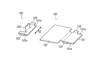
- a perspective view of the anode lead terminal 120 and the cathode lead terminal 130 of the electrolytic capacitor 100 shown in FIG. 1 is schematically shown in FIG.
- a cross-sectional view of the anchor portion of the anode lead terminal 120 is shown in FIG.
- a cross-sectional view of the anchor portion of the cathode lead terminal 130 is shown in FIG.
- FIG. 3 and FIG. 4 the position of the capacitor element 110 is shown by a dotted line.
- the bottom view of the electrolytic capacitor 100 shown in FIG. 1 is schematically shown in FIG.
- FIG. 5 the portion embedded in the exterior resin 101 is shown by a dotted line.
- FIG. 6 a cross-sectional view of the electrolytic capacitor 100 shown in FIG. 1 is schematically shown in FIG.
- the cross-sectional view of FIG. 6 is a cross-sectional view passing through the central axis of the anode lead (anode wire) 112.
- the exterior resin 101 is shown only by the outline represented by the dotted line.
- the electrolytic capacitor 100 has a bottom surface 100B and a top surface 100T on the opposite side of the bottom surface 100B.
- the electrolytic capacitor 100 includes a capacitor element 110, an anode lead terminal 120, a cathode lead terminal 130, a conductive member 141, and an exterior resin 101.
- the anode lead terminal 120 and the cathode lead terminal 130 are each electrically connected to the capacitor element 110.
- the anode lead terminal 120 includes an anode terminal portion 121, a wire connecting portion 122, and two anchor portions 123.
- the anode terminal portion 121 is exposed on the bottom surface 100B.
- the wire connecting portion 122 rises from the anode terminal portion 121 toward the upper surface 100T.
- the groove portion of the wire connecting portion 122 for receiving the tip of the anode lead 112 is formed by resistance welding the anode lead 112 and the wire connecting portion 122.
- the anode lead 112 and the wire connecting portion 122 may be connected by welding, soldering, or the like.
- the two anchor portions 123 extend from the two end sides 121E, respectively.
- the two end sides 121E are the ends of the anode terminal portion 121, and are a pair of end sides along the direction D1 in which the anode lead 112 extends.
- each of the two anchor portions 123 includes an upright portion 123A that rises from the end side 121E toward the upper surface 100T, and an extension portion 123B that bends and extends from the upper end of the upright portion 123A.
- the two anchor portions 123 are bent in different directions at the boundary between the anode terminal portion 121 and the standing portion 123A and the boundary between the standing portion 123A and the extending portion 123B, respectively.
- one surface (the surface on the upper surface 100T side) of the metal sheet constituting the anode lead terminal 120 has a valley fold at the boundary between the anode terminal portion 121 and the standing portion 123A, and the standing portion 123A and the standing portion 123A. It is a mountain fold at the boundary with the extending portion 123B.
- the extending portion 123B extends from the upper end of the standing portion 123A toward the outside of the electrolytic capacitor 100. That is, the extending portions 123B of the two anchor portions 123 are bent from the upper end of the upright portion 123A, respectively, and are oriented away from each other in a direction (D2) perpendicular to the direction (D1) in which the anode lead 112 extends. It is extending.
- the direction in which the extending portion 123B extends is substantially parallel to the bottom surface 100B, and for example, the angle formed by the two may be in the range of ⁇ 20 ° to 20 °.
- the cathode lead terminal 130 includes a cathode terminal portion 131, a connecting portion 132, and two anchor portions 133.
- the cathode terminal portion 131 is exposed on the bottom surface 100B.
- the connecting portion 132 rises from the anode terminal portion 121 toward the upper surface 100T.
- the connecting portion 132 is electrically connected to the cathode portion 115 (cathode layer 117) described later via the conductive member 141. That is, the cathode terminal portion 131 is electrically connected to the capacitor element 110 via the connecting portion 132 and the conductive member 141.
- the conductive member 141 is not particularly limited, and a known conductive member may be used.
- the conductive member 141 may be formed of a metal paste or the like.
- the two anchor portions 133 each extend from the two end sides 131E.
- the two end sides 131E are the ends of the cathode terminal portion 131, and are a pair of end sides along the direction D1 in which the anode lead 112 extends.
- each of the two anchor portions 133 includes an upright portion 133A that rises from the end side 131E toward the upper surface 100T, and an extension portion 133B that bends and extends from the upper end of the upright portion 133A.
- the boundary between the cathode terminal portion 131 and the standing portion 133A and the boundary between the standing portion 133A and the extending portion 133B are bent in different directions. That is, the extending portions 133B of the two anchor portions 133 are bent from the upper end of the upright portion 133A, respectively, and are oriented away from each other in a direction (D2) perpendicular to the direction (D1) in which the anode lead 112 extends. It is extending.
- the direction in which the extending portion 133B extends is substantially parallel to the bottom surface 100B, and for example, the angle formed by the two may be in the range of ⁇ 20 ° to 20 °.
- the distance L1 from the surface of the anode terminal portion 121 to the lower surface of the extending portion 123B may be 50 ⁇ M or more (for example, 75 ⁇ M or more or 100 ⁇ M or more).
- the distance L1 By setting the distance L1 to 50 ⁇ M or more (for example, 75 ⁇ M or more or 100 ⁇ M or more), it becomes easy to fill the lower portion of the extending portion 123B with the exterior resin 101.
- the upper surface of the extending portion 123B is located below the lower surface of the capacitor element 110, but the extending portion 123B is located at a higher position unless the extending portion 123B interferes with the capacitor element 110. You may.
- the distance L3 from the surface of the cathode terminal portion 131 to the lower surface of the extending portion 133B may be 50 ⁇ M or more (for example, 75 ⁇ M or more or 100 ⁇ M or more), and may be in the range of 50 ⁇ M to 500 ⁇ M (for example, 75 ⁇ M). It may be in the range of ⁇ 200 ⁇ M).
- the distance L4 from the upper surface of the extending portion 133B to the lower surface of the capacitor element 110 may be 50 ⁇ M or more (for example, 75 ⁇ M or more or 100 ⁇ M or more), and is in the range of 50 ⁇ M to 500 ⁇ M (for example, the range of 75 ⁇ M to 200 ⁇ M). May be good.
- the horizontal distance W1 (distance along the direction D2) from the end side 121E to the tip of the extending portion 123B and the horizontal distance W2 (distance along the direction D2) from the end side 131E to the tip of the extending portion 133B are Each may be 50 ⁇ M or more (for example, 75 ⁇ M or more or 100 ⁇ M or more).
- the horizontal distances W1 and W2 may be set to 200 ⁇ M or more, respectively.
- the shapes of the anode lead terminal 120 and the cathode lead terminal 130 described above are examples, and are not limited to the above shapes.
- either the anode lead terminal 120 or the cathode lead terminal 130 may not include an anchor portion.
- the connecting portion of the cathode lead terminal 130 does not have to be at the position shown in the figure and may not have the shape shown in the figure as long as it is electrically connected to the cathode portion 115 (cathode layer 117).
- the capacitor element 110 includes an anode portion 111 and a cathode portion 115.
- the anode portion 111 includes an anode body 113 having a dielectric layer 114 formed on its surface, and an anode lead 112.
- the cathode portion 115 includes an electrolyte layer 116 arranged so as to cover the dielectric layer 114, and a cathode layer 117.
- the cathode layer 117 includes, for example, a carbon layer formed on the electrolyte layer 116 and a metal particle layer formed on the carbon layer.
- the metal particle layer is, for example, a layer formed by using a metal paste.
- the anode portion 111 of the capacitor element 110 is electrically connected to the anode lead terminal 120, and the cathode portion 115 of the capacitor element 110 is electrically connected to the cathode lead terminal 130.
- the electrolytic capacitor 100 When the electrolytic capacitor 100 is mounted on a substrate or the like of an electronic device, it may be mounted by soldering the anode terminal portion 121 and the cathode terminal portion 131, respectively.
- the capacitor element 110, the anode lead terminal 120, and the cathode lead terminal 130 are prepared.
- the method for manufacturing the capacitor element 110 is not particularly limited, and the capacitor element 110 can be manufactured by a known method.
- the anode lead terminal 120 and the cathode lead terminal 130 can be formed by a known metal processing method.
- the anode lead 112 and the anode lead terminal 120 are connected, and the cathode layer 117 and the cathode lead terminal 130 are connected.
- the anode lead 112 and the anode lead terminal 120 can be connected by welding (for example, laser welding) or the like.
- the connection between the cathode layer 117 and the cathode lead terminal 130 can be performed by, for example, the following method. First, a metal paste to be a conductive member 141 is applied to the surface of the connecting portion 132 of the cathode lead terminal 130 and / or the surface of the cathode layer 117.
- the cathode layer 117 and the connecting portion 132 are adhered to each other via the metal paste, and the metal paste is cured to form the metal paste into the conductive member 141. In this way, the cathode layer 117 and the cathode lead terminal 130 can be connected.
- the capacitor element is sealed with the material of the exterior resin 101 (for example, mold resin).
- the sealing step can be carried out by a known method.
- the electrolytic capacitor 100 can be manufactured.
- the other electrolytic capacitors disclosed in the present disclosure can also be manufactured by the same manufacturing method.
- This disclosure can be used for electrolytic capacitors.
- Electrolytic capacitor 100B Bottom surface 100T: Top surface 101: Exterior resin 110: Capacitor element 112: Anode lead 120: Anode lead terminal 121: Anode terminal portion 121E, 131E: End side 123, 133: Anchor portion 123A: Standing portion 123B: Extension part 130: Cathode lead terminal 131: Cathode terminal part 131E: End side 133A: Standing part 133B: Extension part D1, D2: Direction
Landscapes
- Engineering & Computer Science (AREA)
- Power Engineering (AREA)
- Microelectronics & Electronic Packaging (AREA)
- Fixed Capacitors And Capacitor Manufacturing Machines (AREA)
- Electric Double-Layer Capacitors Or The Like (AREA)
Priority Applications (4)
| Application Number | Priority Date | Filing Date | Title |
|---|---|---|---|
| JP2022510024A JP7748640B2 (ja) | 2020-03-23 | 2021-03-18 | 電解コンデンサ |
| CN202180021533.6A CN115298776B (zh) | 2020-03-23 | 2021-03-18 | 电解电容器 |
| US17/821,708 US12148578B2 (en) | 2020-03-23 | 2022-08-23 | Electrolytic capacitor |
| US18/920,298 US20250046526A1 (en) | 2020-03-23 | 2024-10-18 | Electrolytic capacitor |
Applications Claiming Priority (2)
| Application Number | Priority Date | Filing Date | Title |
|---|---|---|---|
| JP2020-050694 | 2020-03-23 | ||
| JP2020050694 | 2020-03-23 |
Related Child Applications (1)
| Application Number | Title | Priority Date | Filing Date |
|---|---|---|---|
| US17/821,708 Continuation US12148578B2 (en) | 2020-03-23 | 2022-08-23 | Electrolytic capacitor |
Publications (1)
| Publication Number | Publication Date |
|---|---|
| WO2021193328A1 true WO2021193328A1 (ja) | 2021-09-30 |
Family
ID=77890242
Family Applications (1)
| Application Number | Title | Priority Date | Filing Date |
|---|---|---|---|
| PCT/JP2021/010995 Ceased WO2021193328A1 (ja) | 2020-03-23 | 2021-03-18 | 電解コンデンサ |
Country Status (4)
| Country | Link |
|---|---|
| US (2) | US12148578B2 (https=) |
| JP (1) | JP7748640B2 (https=) |
| CN (1) | CN115298776B (https=) |
| WO (1) | WO2021193328A1 (https=) |
Cited By (1)
| Publication number | Priority date | Publication date | Assignee | Title |
|---|---|---|---|---|
| WO2023106281A1 (ja) * | 2021-12-09 | 2023-06-15 | パナソニックIpマネジメント株式会社 | 電解コンデンサ |
Families Citing this family (1)
| Publication number | Priority date | Publication date | Assignee | Title |
|---|---|---|---|---|
| CN115298776B (zh) * | 2020-03-23 | 2026-04-21 | 松下知识产权经营株式会社 | 电解电容器 |
Citations (3)
| Publication number | Priority date | Publication date | Assignee | Title |
|---|---|---|---|---|
| JP2001110676A (ja) * | 1999-10-05 | 2001-04-20 | Matsuo Electric Co Ltd | チップコンデンサ |
| JP2006270014A (ja) * | 2004-10-15 | 2006-10-05 | Matsushita Electric Ind Co Ltd | 固体電解コンデンサ及びその製造方法とこれを用いたデジタル信号処理基板 |
| JP2007035691A (ja) * | 2005-07-22 | 2007-02-08 | Matsushita Electric Ind Co Ltd | 固体電解コンデンサ及びその製造方法 |
Family Cites Families (10)
| Publication number | Priority date | Publication date | Assignee | Title |
|---|---|---|---|---|
| JP2003068576A (ja) * | 2001-08-30 | 2003-03-07 | Rohm Co Ltd | 面実装型固体電解コンデンサの構造及びその製造方法 |
| JP4450378B2 (ja) * | 2004-10-27 | 2010-04-14 | Necトーキン株式会社 | 表面実装型コンデンサ及びその製造方法 |
| JP4862204B2 (ja) * | 2007-12-06 | 2012-01-25 | 三洋電機株式会社 | 固体電解コンデンサ |
| JP5041995B2 (ja) * | 2007-12-07 | 2012-10-03 | 三洋電機株式会社 | 固体電解コンデンサ |
| WO2012140836A1 (ja) * | 2011-04-14 | 2012-10-18 | パナソニック株式会社 | 電解コンデンサ |
| KR20150049918A (ko) | 2013-10-31 | 2015-05-08 | 삼성전기주식회사 | 탄탈륨 캐패시터 및 그 제조 방법 |
| WO2017056492A1 (ja) * | 2015-09-30 | 2017-04-06 | パナソニックIpマネジメント株式会社 | 固体電解コンデンサ |
| CN115298776B (zh) * | 2020-03-23 | 2026-04-21 | 松下知识产权经营株式会社 | 电解电容器 |
| CN116635964A (zh) * | 2020-12-25 | 2023-08-22 | 松下知识产权经营株式会社 | 电解电容器 |
| WO2022138223A1 (ja) * | 2020-12-25 | 2022-06-30 | パナソニックIpマネジメント株式会社 | 電解コンデンサ |
-
2021
- 2021-03-18 CN CN202180021533.6A patent/CN115298776B/zh active Active
- 2021-03-18 WO PCT/JP2021/010995 patent/WO2021193328A1/ja not_active Ceased
- 2021-03-18 JP JP2022510024A patent/JP7748640B2/ja active Active
-
2022
- 2022-08-23 US US17/821,708 patent/US12148578B2/en active Active
-
2024
- 2024-10-18 US US18/920,298 patent/US20250046526A1/en active Pending
Patent Citations (3)
| Publication number | Priority date | Publication date | Assignee | Title |
|---|---|---|---|---|
| JP2001110676A (ja) * | 1999-10-05 | 2001-04-20 | Matsuo Electric Co Ltd | チップコンデンサ |
| JP2006270014A (ja) * | 2004-10-15 | 2006-10-05 | Matsushita Electric Ind Co Ltd | 固体電解コンデンサ及びその製造方法とこれを用いたデジタル信号処理基板 |
| JP2007035691A (ja) * | 2005-07-22 | 2007-02-08 | Matsushita Electric Ind Co Ltd | 固体電解コンデンサ及びその製造方法 |
Cited By (1)
| Publication number | Priority date | Publication date | Assignee | Title |
|---|---|---|---|---|
| WO2023106281A1 (ja) * | 2021-12-09 | 2023-06-15 | パナソニックIpマネジメント株式会社 | 電解コンデンサ |
Also Published As
| Publication number | Publication date |
|---|---|
| US20250046526A1 (en) | 2025-02-06 |
| JPWO2021193328A1 (https=) | 2021-09-30 |
| JP7748640B2 (ja) | 2025-10-03 |
| CN115298776B (zh) | 2026-04-21 |
| US12148578B2 (en) | 2024-11-19 |
| CN115298776A (zh) | 2022-11-04 |
| US20220399169A1 (en) | 2022-12-15 |
Similar Documents
| Publication | Publication Date | Title |
|---|---|---|
| US20250046526A1 (en) | Electrolytic capacitor | |
| US12255027B2 (en) | Electrolytic capacitor | |
| US12148577B2 (en) | Electrolytic capacitor | |
| CN115298777B (zh) | 电解电容器 | |
| JPWO2021193328A5 (https=) | ||
| WO2022138223A1 (ja) | 電解コンデンサ | |
| CN114981905B (zh) | 电解电容器 | |
| JP2007081069A (ja) | チップ型固体電解コンデンサおよび端子ならびに端子の製造方法 | |
| JP7496517B2 (ja) | 電解コンデンサおよびその製造方法 | |
| JP7850940B2 (ja) | 固体電解コンデンサおよび固体電解コンデンサの製造方法 | |
| CN116724370A (zh) | 电解电容器 | |
| US20240412927A1 (en) | Solid electrolytic capacitor | |
| JP2025130168A (ja) | 電解コンデンサ | |
| WO2024195339A1 (ja) | 電解コンデンサおよびその製造方法 | |
| JP2026059405A (ja) | 電解コンデンサ | |
| JP2022149517A (ja) | 電解コンデンサ | |
| WO2018159426A1 (ja) | 電解コンデンサ | |
| JP2022085762A (ja) | 電解コンデンサ | |
| JP2025056499A (ja) | 電解コンデンサ | |
| JP2002175937A (ja) | チップ固体電解コンデンサ |
Legal Events
| Date | Code | Title | Description |
|---|---|---|---|
| 121 | Ep: the epo has been informed by wipo that ep was designated in this application |
Ref document number: 21775889 Country of ref document: EP Kind code of ref document: A1 |
|
| ENP | Entry into the national phase |
Ref document number: 2022510024 Country of ref document: JP Kind code of ref document: A |
|
| NENP | Non-entry into the national phase |
Ref country code: DE |
|
| 122 | Ep: pct application non-entry in european phase |
Ref document number: 21775889 Country of ref document: EP Kind code of ref document: A1 |