WO2021192247A1 - Puce d'analyse électrochimique - Google Patents
Puce d'analyse électrochimique Download PDFInfo
- Publication number
- WO2021192247A1 WO2021192247A1 PCT/JP2020/014117 JP2020014117W WO2021192247A1 WO 2021192247 A1 WO2021192247 A1 WO 2021192247A1 JP 2020014117 W JP2020014117 W JP 2020014117W WO 2021192247 A1 WO2021192247 A1 WO 2021192247A1
- Authority
- WO
- WIPO (PCT)
- Prior art keywords
- sample liquid
- electrode
- flow path
- substrate
- chip
- Prior art date
Links
Images


Classifications
-
- G—PHYSICS
- G01—MEASURING; TESTING
- G01N—INVESTIGATING OR ANALYSING MATERIALS BY DETERMINING THEIR CHEMICAL OR PHYSICAL PROPERTIES
- G01N27/00—Investigating or analysing materials by the use of electric, electrochemical, or magnetic means
- G01N27/26—Investigating or analysing materials by the use of electric, electrochemical, or magnetic means by investigating electrochemical variables; by using electrolysis or electrophoresis
- G01N27/28—Electrolytic cell components
- G01N27/30—Electrodes, e.g. test electrodes; Half-cells
Definitions
- the present invention relates to an electrochemical analysis chip for measuring the concentration of a specific substance that can be contained in a sample solution.
- Measurements using the principle of electrochemical measurement are represented by high-sensitivity measurement of heavy metals in solution, glucose measurement using enzyme electrodes, pH (pH) measurement using ion electrodes, and electrochemical detection of residual pesticides. It is used in many situations such as food inspection (see, for example, Patent Document 1).
- an electrochemical analysis chip in which electrodes are formed on an insulating substrate can be used.
- the electrode basically has a single-layer structure, and as the electrode material, a metal material such as silver, platinum, gold, or aluminum, or a conductive material such as carbon is used.
- the present invention has been made to improve the above situation, and an object of the present invention is to provide an electrochemical analysis chip capable of measuring a plurality of items with one sampling operation.
- the electrochemical analysis chip of the present invention includes a sensor portion provided on the insulating base material and having a plurality of electrodes, and a flow path portion provided on the base material and guiding the sample liquid to the sensor portion.
- the base material is provided with a plurality of the sensor units, and the flow path portion uses the same sample liquid as the sample liquid supply port opened on the outer surface of the base material. It is provided with a sample liquid flow path leading to the plurality of sensor units.
- the same sample liquid can be guided from the sample liquid supply port to a plurality of sensor units by the sample liquid flow path, so that the same sample liquid can be used for a plurality of sensor units in one sampling operation.
- the sample liquid can be brought into contact. This makes it possible to measure a plurality of items with one sampling operation even with a small amount of sample liquid.
- the flow path portion may include a plurality of the sample liquid flow paths connected to one sample liquid supply port.
- the sample liquid can be introduced into a plurality of sensor units simply by bringing the sample liquid into contact with one sample liquid supply port, so that the sampling operation is easy and the time required for the sampling operation is shortened. It can be timed.
- the flow path portion includes the sample liquid supply port and the sample liquid flow path for each of the plurality of sensor units, and the plurality of sample liquid supply ports are the bases. It may be arranged close to each other on the outer surface of the material.
- the sample liquid can be reliably introduced into each sensor unit. Further, since the sample liquid supply ports provided for each sensor unit are arranged close to each other on the outer surface of the base material, the sample liquid can be reliably brought into contact with the sample liquid supply ports by one sampling operation. It is possible to improve the certainty of the sampling process.
- the sensor unit is provided on an electrode chip that can be attached to the base material, and the base material is opened to the outer surface of the base material into which the electrode chip is inserted.
- An electrode chip arranging portion is provided, the sample liquid flow path is connected to the electrode chip arranging portion, and the sample liquid is formed between the inner wall of the electrode chip arranging portion and the electrode chip by a capillary phenomenon.
- a gap may be provided for permeation from the liquid flow path toward the opening of the electrode chip arrangement portion.
- the base material is a laminate of a base substrate on which the sensor portion is formed, a flow path substrate forming the flow path portion, and a cover substrate covering the flow path substrate. It may be configured.
- the electrochemical analysis chip can be miniaturized by integrating the sensor unit with the base substrate.
- the sensor unit includes a working electrode and a reference electrode as the electrodes, or a working electrode and a reference electrode and a counter electrode, and the electrode is an insulating substrate.
- a metal layer formed on the metal layer, a carbon layer formed on the substrate so as to cover the metal layer, and an upper adhesive layer formed between the upper surface of the metal layer and the carbon layer are provided.
- the upper adhesive layer may be made of silicon.
- each electrode since each electrode has a metal layer, the electric resistance can be lowered and the measurement sensitivity can be improved. Further, by covering the metal layer with a carbon layer, redox of the metal layer can be prevented, and measurement sensitivity and reproducibility can be improved. Furthermore, by providing an upper adhesive layer made of silicon between the upper surface of the metal layer and the carbon layer, the adhesion between the metal layer and the carbon layer is improved, and silicon has a higher electrical resistivity than metal. Since it is high, it is possible to suppress the generation of hydrogen on the upper surface of the metal layer during measurement, prevent the metal layer and the carbon layer from peeling off, and improve the measurement sensitivity and reproducibility.
- the present invention can provide an electrochemical analysis chip capable of measuring a plurality of items with one sampling.
- FIG. 5 is a plan view showing still another embodiment of the electrochemical analysis chip. It is a separation perspective view of the same electrochemical analysis chip.
- FIG. 1 is a schematic configuration diagram showing an example of an electrochemical measuring device.
- FIG. 2 is a plan view showing an embodiment of an electrochemical analysis chip.
- FIG. 3 is a separated perspective view of the electrochemical analysis chip.
- FIG. 4 is a side view central longitudinal sectional view of the electrochemical analysis chip. In FIG. 2, the cover substrate 213 is not shown. Further, in FIG. 4, for convenience, the thickness of each member is increased.
- the electrochemical measuring device 1 includes an electrochemical analysis chip 2, a potentiostat 3 connected to the electrochemical analysis chip 2, an operation unit 4 and a display unit 5 connected to the electrochemical analysis chip 3. It includes a power supply unit 6 and an external output unit 7.
- the electrochemical analysis chip 2 is a disposable type.
- the electrochemical analysis chip 2 is provided with an insulating base material 21, a plurality of sensor units 22 provided on the base material 21, and a sample solution provided on the base material 21. It is provided with a flow path portion 23 that leads to the sensor portion 22.
- the number of sensor units may be two or four or more.
- the base material 21 is configured such that the cover substrate 213 is arranged on the base substrate 211 via the flow path substrate 212.
- the base substrate 211, the flow path substrate 212, and the cover substrate 213 are composed of a substantially quadrangular insulating substrate.
- the flow path substrate 212 has a notch portion 214 into which an electrode chip 24 having a sensor portion 22 can be inserted, a groove 215 for forming a sample liquid supply port 231 forming the flow path portion 23, and a sample liquid flow path 232. Is formed. In this embodiment, three notches 214 are formed.
- the notch portion 214 is open to the first side surface 212a of the flow path substrate 212, and is formed with a width dimension slightly larger than the width dimension of the electrode chip 24.
- the notch portion 214 is covered with the base substrate 211 and the cover substrate 213 to form the electrode chip arranging portion 216.
- the groove 215 is formed on one surface of the flow path substrate 212, extends from the second side surface 212b facing the first side surface 212a of the flow path substrate 212 toward the first side surface 212a, and branches into three in the middle portion. It is connected to three notches 214.
- a plurality of sample liquids that are the same as the sample liquid supply port 231 opened on the outer surface of the base material 21 (second side surface 212b of the flow path substrate 212) are provided from the sample liquid supply port 231.
- a flow path portion 23 having a sample liquid flow path 232 leading to the sensor portion 22 of the above is formed.
- the material of the insulating substrate constituting the base substrate 211, the flow path substrate 212 and the cover substrate 213 is not particularly limited, and for example, glass, quartz glass, polyimide (PI), polyethylene terephthalate (PET), polycarbonate (PC), polyethylene. (PE), polypropylene (PP), polystyrene (PS), polyvinyl chloride (PVC), polyoxymethylene (POM), ABS resin (ABS), methacrylic resin (PMMA) and the like can be mentioned. Further, the shape, thickness and size of the insulating substrate are not particularly limited.
- sample liquid supply port 231 and the sample liquid flow path 232 are as long as the sample liquid can be introduced from the sample liquid supply port 231 into the sample liquid flow path 232 by capillary action and guided to the sensor unit 22. good.
- a hydrophilic treatment layer for improving wettability may be formed on the inner wall surface of the sample liquid flow path 232 (the inner wall surface of the groove 215 and the joint surface of the cover substrate 213 with the flow path substrate 212).
- the base material 21 of the electrochemical analysis chip 2 is formed by laminating the base substrate 211, the flow path substrate 212, and the cover substrate 213 in this order and integrating them.
- an adhesive or heat fusion can be used for joining the base substrate 211 and the flow path substrate 212, and joining the flow path substrate 212 and the cover substrate 213, for example.
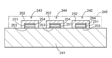
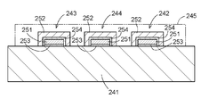
- the electrode tip 24 includes a flat plate-shaped insulating substrate 241, and a working electrode 242, a counter electrode 243, and a reference electrode 244 are provided on the substrate 241 so as to be insulated from each other.
- the substrate 241 has a substantially rectangular shape in a plan view.
- the working electrode 242, the counter electrode 243, and the reference electrode 244 are provided from the vicinity of one end to the vicinity of the other end in the longitudinal direction of the substrate 241.
- the longitudinal intermediate portion of the working electrode 242, the counter electrode 243 and the reference electrode 244 is covered with an insulating layer 245 formed on the substrate 241.
- One end side of the working electrode 242, the counter electrode 243 and the reference electrode 244 constitutes a sensor unit 22.
- the sensor portion 22 By inserting one end side of the electrode chip 24 into the electrode chip arrangement portion 216 of the base material 21, the sensor portion 22 (one end side of the working electrode 242, the counter electrode 243 and the reference electrode 244) is arranged inside the electrode chip arrangement portion 216. Will be done. Between the inner wall of the electrode tip arranging portion 216 and the electrode tip 24, the sample liquid introduced into the flow path portion 23 by the capillary phenomenon is introduced to the opening side (first side surface 212a side) of the electrode chip arranging portion 216 by the capillary phenomenon. A small gap is formed to the extent that it penetrates into.
- the size of the gap between the inner wall of the electrode tip arranging portion 216 and the electrode tip 24 is such that the sample liquid permeates from the sample liquid flow path 232 toward the opening of the electrode chip arranging portion 216 due to the capillary phenomenon. If so, there is no particular limitation. Further, the inner wall surface of the electrode chip arranging portion 216 (the inner wall surface of the notch portion 214, the joint surface of the base substrate 211 with the flow path substrate 212, and the joint surface of the cover substrate 213 with the flow path substrate 212) is made wet.
- the hydrophilic treatment layer to be improved may be formed.
- the working electrode 242, the counter electrode 243, and the other end side of the reference electrode 244 located on the other end side of the electrode tip 24 are arranged outside the base material 21 and are potentiometers via the connector 8 and the cable 9 (see FIG. 2). It is electrically connected to 3 (see FIG. 1).
- the electrode tip 24 is detachably attached to the connector 8.
- the sample liquid When the sample liquid is supplied to the sample liquid supply port 231 of the electrochemical analysis chip 2, the sample liquid is formed in the sample liquid flow path 232 by the capillary phenomenon, respectively, of the three electrode chip arrangement portions 216 (notch portions 214). And is introduced into each electrode tip arranging portion 216.
- the sample liquid introduced into the electrode chip arranging portion 216 has a gap between the electrode chip arranging portion 216 and the electrode chip 24 toward the opening side (first side surface 212a side) of the electrode chip arranging portion 216 due to the capillary phenomenon. It flows and comes into contact with the sensor portion 22 of the electrode chip 24.
- the electrochemical analysis chip 2 of the present embodiment has a sensor unit 22 having a plurality of electrodes 242, 243, 244 and provided on the insulating base material 21, and the base material 21. It is provided with a flow path portion 23 for guiding the sample liquid to the sensor portion 22.
- a plurality of sensor units 22 are provided on the base material 21, and the flow path portion 23 has a plurality of sensors that provide the same sample liquid as the sample liquid supply port 231 opened on the outer surface of the base material 21 from the sample liquid supply port 231. It is provided with a sample liquid flow path 232 leading to the portion 22.
- the same sample liquid can be guided from the sample liquid supply port 231 to the plurality of sensor units 22 by the sample liquid flow path 232, so that the same sample liquid can be connected to the plurality of sensor units 22 by one sampling operation.
- the same sample liquid can be brought into contact with each other. This makes it possible to measure a plurality of items with one sampling operation even with a small amount of sample liquid.
- the flow path portion 23 includes a plurality of sample liquid flow paths 232 connected to one sample liquid supply port 231.
- the sample liquid can be introduced into a plurality of sensor units 22 simply by bringing the sample liquid into contact with one sample liquid supply port 231. Therefore, the sampling operation is easy and the time required for the sampling operation can be shortened. ..
- the sensor unit 22 is provided on the electrode chip 24 that can be mounted on the base material 21.
- the base material 21 includes an electrode chip arranging portion 216 that opens to the outer surface of the base material 21 and into which the electrode chip 24 is inserted.
- the sample liquid flow path 232 is connected to the electrode tip placement portion 216, and the sample liquid is transferred from the sample liquid flow path 232 to the electrode tip placement portion 216 between the inner wall of the electrode tip placement portion 216 and the electrode tip 24 due to a capillary phenomenon. There is a gap that penetrates toward the opening of the. As a result, by exchanging the electrode chip 24 according to the measurement item, it is possible to correspond to a large number of measurement items, so that the versatility of the electrochemical analysis chip 2 is improved.
- At least one surface of the substrate 241 of the electrode chip 24 is formed of a flat insulating material.
- the substrate 241 include a polyethylene terephthalate film, a polyimide film, a glass substrate, and an epoxy glass (Galaepo) substrate.
- the material of the substrate 241 is not limited to these, and may be ceramics, quartz glass, or the like.
- the working electrode 242, the counter electrode 243, and the reference electrode 244 each have a metal layer 251 formed on the substrate 241 and a carbon layer 252 formed on the substrate 241 so as to cover the metal layer 251. It includes a lower adhesive layer 253 formed between the substrate 241 and the metal layer 251 and an upper adhesive layer 254 formed between the upper surface of the metal layer 251 and the carbon layer 252.
- a silver-silver chloride layer 255 is formed on the upper surface of the carbon layer 252 on one end side of the reference electrode 244.
- the lower adhesive layer 253 is a thin film that prevents the substrate 241 and the metal layer 251 from peeling off, and is formed of, for example, silicon.
- the material of the lower adhesive layer 253 may be any material as long as it has good adhesion to the substrate 241 and the metal layer 251.
- chromium and titanium a metal covalently bonded to carbon can be used.
- the metal layer 251 is made of a material having a lower electrical resistivity than the carbon layer 252, and is formed on the lower adhesive layer 253.
- the metal layer 251 is for reducing the electrical resistance between one end and the other end of each of the working electrode 242, the counter electrode 243 and the reference electrode 244.
- the upper adhesive layer 254 is formed on the upper surface of the metal layer 251 and is a thin film that prevents the upper surface of the metal layer 251 and the carbon layer 252 from peeling off, and is made of silicon.
- the carbon layer 252 is formed on the substrate 241 so as to cover the lower adhesive layer 253, the metal layer 251 and the upper adhesive layer 254.
- the carbon layer 252 is formed of, for example, amorphous carbon or diamond-like carbon (DLC). Further, the carbon layer 252 is formed so as to surround the contours of the lower adhesive layer 253, the metal layer 251 and the upper adhesive layer 254 in a plan view, and the lower peripheral edge portion of the carbon layer 252 is in contact with the substrate 241.
- the lower adhesive layer 253, the metal layer 251 and the upper adhesive layer 254 are isolated from the surrounding atmosphere by being surrounded by the substrate 241 and the carbon layer 252.
- carbon Since carbon has the following characteristics, it is suitable for use of the carbon layer 252 that protects the metal layer 251. (1) Has excellent stability even in a vacuum of 3000 ° C (in air at 500 ° C), (2) is not easily attacked by chemicals, (3) does not allow gas or solution to permeate, (4) excellent hardness, Strong, (5) excellent electrical conductivity, (6) resistant to wetting of metal salts, etc., (7) good blood and tissue compatibility, (8) physical and chemical properties Is isotropic.
- a vapor deposition method is preferable because the shape and film thickness of each layer can be controlled with high accuracy.
- a so-called physical vapor deposition method PVD
- a so-called physical vapor deposition method PVD
- a vacuum vapor deposition method ion plating method, or a sputtering method
- a so-called chemical vapor deposition method CVD
- the method for producing each layer is not limited to the vapor deposition method, and may be a printing method such as a screen printing method or an inkjet printing method.
- the electrodes 242, 243, and 244 include a metal layer 251 formed on the insulating substrate 241, a carbon layer 252 formed on the substrate 241 so as to cover the metal layer 251, and the substrate 241. It includes a lower adhesive layer 253 formed between the metal layer 251 and the metal layer 251.
- the electric resistance can be lowered and the measurement sensitivity can be improved.
- the redox of the metal layer 251 can be prevented, and the measurement sensitivity and reproducibility can be improved.
- the upper adhesive layer 254 made of silicon between the upper surface of the metal layer 251 and the carbon layer 252
- the adhesion between the metal layer 251 and the carbon layer 252 is improved, and silicon is more electric than the metal. Since the resistivity is high, it is possible to suppress the generation of hydrogen on the upper surface of the metal layer 251 during measurement. As a result, peeling of the substrate 241 and the metal layer 251 can be prevented, and measurement sensitivity and reproducibility can be improved.
- the electrodes 242, 243 and 244 include a lower adhesive layer 253 formed between the substrate 241 and the metal layer 251 to prevent deterioration of the adhesion between the substrate 241 and the metal layer 251 during measurement. It is possible to improve the measurement sensitivity and reproducibility.
- the metal layer 251 and the carbon layer 252 and the adhesive layer 253 and 254 are formed by a vapor deposition method, and the metal layer 251 and the adhesive layer 253 and 254 are formed in the same shape in a plan view, and carbon.
- the layer 252 is formed so as to surround the contours of the metal layer 251 and the adhesive layers 253 and 254 in a plan view.
- the lower adhesive layer 253 is made of silicon. Since silicon has good adhesion to glass and metal, the adhesion between the metal layer 251 and the substrate 241 can be strengthened.
- the upper adhesive layer 254 is also made of silicon. Since silicon has good adhesion to metal and carbon, it is possible to strengthen the adhesion between the metal layer 251 and the carbon layer 252.
- the sensor unit 22 includes a working electrode 242, a reference electrode 244, and a counter electrode 243, it can be applied to a three-electrode electrochemical measurement.
- the electrical resistance of the working electrode 242, the reference electrode 244, and the counter electrode 243 can be lowered, the redox of the metal layer 251 can be prevented, and the metal layer 251 can be prevented from peeling off, so that the measurement sensitivity and reproducibility can be improved. ..
- the sensor unit 22 may be provided with two electrodes used in a two-electrode electrochemical measurement using a working electrode 242 and a reference electrode 244. If both the working electrode and the reference electrode are composed of an electrode having a metal layer, a carbon layer and an adhesive layer, the electrical resistance of both the working electrode and the reference electrode can be lowered, and the metal layer can be oxidized. Since reduction can be prevented and peeling of the metal layer can be prevented, measurement sensitivity and reproducibility can be improved.
- the working electrode 242, the counter electrode 243 and the reference electrode 244 of the sensor unit 22 are not limited to the above structure, and are, for example, a single-layer structure of a metal material such as silver, platinum, gold, aluminum or palladium, or a conductivity such as carbon. It may be a single-layer structure of a sex material or a laminated structure in which a plurality of these materials are laminated. Further, the lower adhesive layer 253 may not be provided on the electrodes 242, 243, and 244.
- the potentiostat 3 controls the potential of the working electrode 242 of the electrode tip 24 to be constant with respect to the reference electrode 244, and transfers the current flowing between the working electrode 242 and the counter electrode 243. It is configured to be measurable.
- the potentiostat 3 includes an arithmetic control unit 31, a voltage application unit 32, and a current detection unit 33 as a schematic configuration.
- the arithmetic control unit 31 performs a predetermined arithmetic processing using the measured values obtained by the electrochemical measurement, and is required for the voltage application unit 32 based on a command from the user input via the operation unit 4. It is a function of transmitting a signal and displaying information such as a measurement result on the display unit 5.
- the arithmetic control unit 31 is realized by, for example, a microcomputer executing a predetermined program.
- the voltage application unit 32 When the voltage application unit 32 receives the measurement start signal from the arithmetic control unit 31, the voltage application unit 32 applies a voltage having a desired waveform between the working electrode 242 and the counter electrode 243 of the electrode chip 24 to and the working electrode 242. It is configured to control the potential between the reference electrode 244 and the reference electrode 244 to be a desired potential.
- the current detection unit 33 is configured to detect the magnitude of the current flowing between the working electrode 242 of the electrode tip 24 and the counter electrode 243. A signal relating to the magnitude of the current detected by the current detection unit 33 is taken into the arithmetic control unit 31.
- the arithmetic control unit 31 calculates the concentration of a specific component in the sample solution based on the signal captured from the current detection unit 33, for example, using a calibration curve prepared in advance, and displays the measurement result on the display unit 5. It is configured as follows.
- the operation unit 4 is an input device for the user to perform operations such as turning on / off the power supply, starting measurement, and changing the information displayed on the display unit 5.
- the display unit 5 is realized by, for example, a liquid crystal display.
- the display unit 5 may be composed of a touch panel, and the display unit 5 may have the functions of the operation unit 4.
- the power supply unit 6 can be realized by, for example, a dry battery or a storage battery. The power supply unit 6 supplies necessary electric power to the potentiostat 3 and the display unit 5.
- an external output unit 7 is connected to the potentiostat 3 so that information can be output to an external device such as a personal computer by a wired communication means such as a USB (universal serial bus) terminal or a wireless communication means. You may.
- the arithmetic control unit 31 is configured to output measurement data or the like to an external device via the external output unit 7.
- the operation unit 4, the display unit 5, the power supply unit 6, and the external output unit 7 may be realized by a mobile computer such as a notebook computer or a tablet, for example. Further, if a small potentiometer 3 (for example, a small potentiometer "miniSTAT100" (manufactured by Biodevice Technology)) is used as the potentiometer 3, the electrochemical measuring device 1 can be configured to be portable. This enables on-site (on-site) measurement of the sample solution using the electrochemical measuring device 1.
- a small potentiometer 3 for example, a small potentiometer "miniSTAT100" (manufactured by Biodevice Technology)
- miniSTAT100 manufactured by Biodevice Technology
- the electrochemical measurement using the electrochemical measuring device 1 is performed in a state where the sample solution is in contact with the sensor unit 22 of the electrochemical analysis chip 2. That is, the measurement is performed in a state where the sample liquid is brought into contact with the sample liquid supply port 231 of the electrochemical analysis chip 2 and the sample liquid is introduced into the sample liquid flow path 232 and the electrode chip arrangement portion 216.
- a silicon layer having a thickness of about 20 nm is placed underneath by a sputtering method using a metal mask having an opening pattern corresponding to the lower adhesive layer forming region. It was formed as an adhesive layer 253.
- the film thickness of the lower adhesive layer 253 made of silicon is not particularly limited.
- a silver layer having a thickness of about 150 nm is formed as a metal layer 251 on the lower adhesive layer 253 by a sputtering method. bottom.
- a silicon layer having a thickness of about 20 nm was formed as the upper adhesive layer 254 on the metal layer 251 by a sputtering method.
- the film thickness of the upper adhesive layer 254 made of silicon is not particularly limited.
- the lower adhesive layer 253, the metal layer 251 and the upper adhesive layer 254 are formed on the substrate 241 without being carried out from the chamber by using the same metal mask. bottom.
- the time required for film formation of the lower adhesive layer 253, the metal layer 251 and the upper adhesive layer 254 can be shortened, and foreign matter can be prevented from adhering between the layers.
- the metal layer 251 and the adhesive layers 253 and 254 are formed in the same shape in a plan view.
- the line width (dimension in the width direction orthogonal to the longitudinal direction) of the lower adhesive layer 253, the metal layer 251 and the upper adhesive layer 254 is about 0.6 mm.
- a carbon layer 252 having a thickness of about 1000 nm is formed so as to cover the lower adhesive layer 253, the metal layer 251 and the upper adhesive layer 254 by using a metal mask having an opening pattern surrounding the lower adhesive layer forming region. bottom.
- the line width of the carbon layer 252 is about 1 mm.
- the lower adhesive layer 253, the metal layer 251 and the upper adhesive layer 254 and the carbon layer 252 are formed by the vapor deposition method (here, the sputtering method) by using a metal mask having an opening pattern, so that each layer can be formed. Since patterning by an etching method or a lift-off method is not required after film formation, the manufacturing cost can be reduced.
- a silver layer having a thickness of about 100 nm was formed on the upper surface of the carbon layer 252 on one end side of the reference electrode 244 by a film forming method, and the silver chloride layer 255 was formed by chlorination treatment. In this way, the electrode tip 24 was manufactured.
- the side surface of the metal layer 251 is in contact with the carbon layer 252, and at the time of electrochemical measurement, the side surface of the metal layer 251 is caused by the water permeating the carbon layer 252.
- the thickness of the metal layer 251 is as thin as 150 nm, even if hydrogen is generated on the side surface of the metal layer 251 the amount of hydrogen is extremely small, which is suitable for measurement. The impact is considered to be small.
- the film thickness of the metal layer 251 is not particularly limited, but is preferably 50 nm or more and 1000 nm or less. This is because if it is within this range, the total resistance value of the electrodes 242, 243 and 244 can be reduced while suppressing the amount of hydrogen generated on the side surface of the metal layer 251 to a small amount. If the film thickness of the metal layer 251 is thinner than 50 nm, the electrodes 242, 243, and 244 have high resistance and the measurement sensitivity is lowered. Further, when the film thickness of the metal layer 251 is thicker than 1000 nm, the influence of hydrogen generated on the side surface of the metal layer 251 on the measurement becomes large.
- the metal layer 251 is formed by a vapor deposition method (for example, a sputtering method)
- a vapor deposition method for example, a sputtering method
- the manufacturing cost can be reduced by providing the regions of the plurality of electrode chips 24 on one substrate 241 to form the plurality of electrode chips 24 at the same time and then separating each electrode chip 24 into individual pieces.
- a metal layer 251 and a carbon layer 252 formed on the substrate 241 without forming the adhesive layers 253 and 254 on the electrode chip 24 were produced and used as a comparative chip.
- a small potentiometer "miniSTAT100" manufactured by Biodevice Technology was used as the potentiometer 3. Electrochemical measurements were performed by differential pulse voltammetry (DPV). The measurement by DPV was carried out by changing the potential of the working electrode from -1500 mV to 300 mV, increasing the potential at 0.004 V, pulse amplitude of 0.05 V, pulse period of 0.2 seconds, and sweeping speed of 0.02 V / s. About 20 ⁇ L of each of the above samples was dropped onto the electrode chip 24 and the comparison chip for measurement. The obtained current potential curve is shown in FIG. In FIG. 7, the vertical axis represents current and the horizontal axis represents potential.
- FIG. 8 is a micrograph of the electrode chip 24 after measurement and the working electrode 242 of the comparison chip taken from the substrate 241 side.
- FIG. 8A shows an embodiment (electrode chip 24), and
- FIG. 8B shows a comparative example (B). Comparison chip) is shown.
- peeling of the metal layer 251 was observed in the comparative chip (B), but peeling of the metal layer and the lower adhesive layer 253 was not observed in the electrode tip of the embodiment (A).
- the upper adhesive layer 254 made of silicon may be formed so as to cover the side surface of the metal layer 251 as well.
- Such an upper adhesive layer 254 can be formed by a vapor deposition method (for example, a sputtering method).
- a vapor deposition method for example, a sputtering method.
- FIG. 10 is a plan view showing another embodiment of the electrochemical analysis chip. Note that in FIG. 10, the cover substrate 213 is not shown.
- the flow path portion 23 includes a sample liquid supply port 231 and a sample liquid flow path 232 for each of the plurality of sensor units 22. That is, the three grooves 215 formed on one surface of the flow path substrate 212A are provided separately from each other. The three sample liquid supply ports 231 formed by one ends of the three grooves 215 are arranged close to each other on the outer surface of the base material 21A (second side surface 212b of the flow path substrate 212A).
- the sample liquid can be reliably introduced into each sensor unit 22. Further, since the sample liquid supply ports 231 provided for each sensor unit 22 are arranged close to each other on the outer surface of the base material 21A, the sample liquid can be reliably sampled in those sample liquid supply ports 231 by one sampling operation. It can be brought into contact with each other, and the certainty of the sampling process can be improved.
- FIG. 11 is a plan view showing still another embodiment of the electrochemical analysis chip.
- FIG. 12 is a separated perspective view of the electrochemical analysis chip. In FIG. 11, the cover substrate 213B is not shown.
- the base material 21B includes a base substrate 211B on which the sensor portion 22 is formed, a flow path substrate 212B forming the flow path portion 23, and a cover substrate 213B covering the flow path substrate 212B. And are laminated.
- Each sensor unit 22 is formed by one end of a working electrode 242, a counter electrode 243, and a reference electrode 244 having the same configuration as the electrodes 242, 243, and 244 of the electrode chip 24 provided on the electrochemical analysis chip 2 of the above embodiment. There is. The other end side of the electrodes 242, 243, 244 is arranged on the connector connecting portion 217 projecting from one side of the base substrate 211B.
- a sample liquid accommodating portion 218 formed of a through hole is formed in place of the notch portion 214 (see FIGS. 2 and 3) provided in the electrochemical analysis chip 2 of the above embodiment. There is.
- the sample liquid accommodating portion 218 is formed at a position surrounding the sensor portion 22 in a state where the base substrate 211B and the flow path substrate 212B are overlapped with each other.
- the flow path substrate 212B is formed with a flow path portion 23 for forming the sample liquid supply port 231 and the sample liquid flow path 232, similarly to the electrochemical analysis chip 2 of the above embodiment.
- the end of the sample liquid flow path 232 opposite to the sample liquid supply port 231 is connected to the sample liquid storage portion 218.
- An air hole 219 is formed in the cover substrate 213B joined to the flow path substrate 212B at a position overlapping the sample liquid accommodating portion 218 in a plan view.
- the sample liquid When the sample liquid is supplied to the sample liquid supply port 231 of the electrochemical analysis chip 2B by the sampling operation, the sample liquid heads toward each of the three sample liquid storage portions 218 in the sample liquid flow path 232 by the capillary phenomenon. It flows and is introduced into each sample liquid storage unit 218 and comes into contact with each sensor unit 22. In this way, the electrochemical analysis chip 2B can bring the same sample solution into contact with the plurality of sensor units 22 in one sampling operation.
- the electrochemical analysis chip 2B can be miniaturized by integrating the plurality of sensor units 22 into the base substrate 211B.
- the configuration in which the sensor unit 22 is integrated with the base substrate 211B can also be applied to a configuration in which the sample liquid supply port 231 and the sample liquid flow path 232 are provided for each sensor unit 22 (see FIG. 10).
- the electrochemical analysis chip may have a configuration in which a working electrode 242 and a reference electrode 244 are provided as electrodes and a counter electrode 243 is not provided, and may be a configuration applicable to a two-electrode electrochemical measurement.
- the position where the sample liquid supply port is arranged is not limited to the side surface of the base material constituting the electrochemical analysis chip, and the sample liquid supply port is one plane surface of the base material (for example, the flow path substrate of the base substrate 211). It may be arranged on the surface opposite to the 212 or the surface of the cover substrate 213 opposite to the flow path substrate 212).
- the electrochemical analysis chip of the present invention is not limited to differential pulse voltammetry (DPV), but includes linear sweep voltammetry (LSV), chronoamperemetry (CA), cyclic voltammetry (CV), short waveform voltammetry (SWV), and the like. It is also applicable to the method.
- DUV differential pulse voltammetry
- LSV linear sweep voltammetry
- CA chronoamperemetry
- CV cyclic voltammetry
- SWV short waveform voltammetry
Landscapes
- Chemical & Material Sciences (AREA)
- Life Sciences & Earth Sciences (AREA)
- Health & Medical Sciences (AREA)
- Physics & Mathematics (AREA)
- Chemical Kinetics & Catalysis (AREA)
- Electrochemistry (AREA)
- Molecular Biology (AREA)
- Analytical Chemistry (AREA)
- Biochemistry (AREA)
- General Health & Medical Sciences (AREA)
- General Physics & Mathematics (AREA)
- Immunology (AREA)
- Pathology (AREA)
- Investigating Or Analyzing Materials By The Use Of Electric Means (AREA)
- Automatic Analysis And Handling Materials Therefor (AREA)
Abstract
La présente invention concerne une puce d'analyse électrochimique avec laquelle il est possible de mesurer une pluralité d'éléments avec un seul échantillonnage. Une puce d'analyse électrochimique (2) comprend : des parties de capteur (22) qui comportent une pluralité d'électrodes (242, 243, 244) et sont disposées sur un substrat isolant (21) ; et une partie de canal (23) qui est disposée sur le substrat (21) et guide un échantillon liquide vers les parties de capteur (22). Une pluralité de parties de capteur (22) sont disposées sur le substrat (21). La partie de canal (23) comprend une entrée d'alimentation en liquide d'échantillon (231) qui est ouverte dans une surface externe du substrat (21) et des canaux de liquide d'échantillon (232) qui guident le liquide d'échantillon depuis l'entrée d'alimentation en liquide d'échantillon (231) jusqu'à la pluralité de parties de capteur (22).
Priority Applications (3)
| Application Number | Priority Date | Filing Date | Title |
|---|---|---|---|
| CN202080099099.9A CN115349088A (zh) | 2020-03-27 | 2020-03-27 | 电化学分析芯片 |
| PCT/JP2020/014117 WO2021192247A1 (fr) | 2020-03-27 | 2020-03-27 | Puce d'analyse électrochimique |
| JP2022510349A JP7325614B2 (ja) | 2020-03-27 | 2020-03-27 | 電気化学分析チップ |
Applications Claiming Priority (1)
| Application Number | Priority Date | Filing Date | Title |
|---|---|---|---|
| PCT/JP2020/014117 WO2021192247A1 (fr) | 2020-03-27 | 2020-03-27 | Puce d'analyse électrochimique |
Publications (1)
| Publication Number | Publication Date |
|---|---|
| WO2021192247A1 true WO2021192247A1 (fr) | 2021-09-30 |
Family
ID=77891620
Family Applications (1)
| Application Number | Title | Priority Date | Filing Date |
|---|---|---|---|
| PCT/JP2020/014117 WO2021192247A1 (fr) | 2020-03-27 | 2020-03-27 | Puce d'analyse électrochimique |
Country Status (3)
| Country | Link |
|---|---|
| JP (1) | JP7325614B2 (fr) |
| CN (1) | CN115349088A (fr) |
| WO (1) | WO2021192247A1 (fr) |
Cited By (1)
| Publication number | Priority date | Publication date | Assignee | Title |
|---|---|---|---|---|
| WO2022153917A1 (fr) * | 2021-01-14 | 2022-07-21 | 光馳科技(上海)有限公司 | Outil de détection génétique et kit de détection génétique |
Citations (6)
| Publication number | Priority date | Publication date | Assignee | Title |
|---|---|---|---|---|
| JPH01291153A (ja) * | 1988-05-18 | 1989-11-22 | Matsushita Electric Ind Co Ltd | バイオセンサ |
| WO1994002631A1 (fr) * | 1992-07-22 | 1994-02-03 | Daikin Industries, Ltd. | Procede et appareil d'inspection concernant des maladies infectieuses |
| JP2004117342A (ja) * | 2002-09-03 | 2004-04-15 | Matsushita Electric Ind Co Ltd | バイオセンサ及びそれを用いた測定法 |
| WO2010004690A1 (fr) * | 2008-07-09 | 2010-01-14 | 日本電気株式会社 | Électrode de carbone, capteur électrochimique, et procédé de fabrication d'une électrode de carbone |
| JP2019105637A (ja) * | 2017-12-11 | 2019-06-27 | 日東電工株式会社 | 電極フィルムおよび電気化学測定システム |
| US20190302097A1 (en) * | 2016-06-06 | 2019-10-03 | Shenzhen Xiaofu Medical Technology Co. | A urine analysis system and a method for urine analysis |
Family Cites Families (8)
| Publication number | Priority date | Publication date | Assignee | Title |
|---|---|---|---|---|
| JP3214561B2 (ja) * | 1998-07-02 | 2001-10-02 | 日本電気株式会社 | 酵素電極およびそれを用いたバイオセンサ、測定器 |
| US7047795B2 (en) * | 2001-08-01 | 2006-05-23 | Arkray, Inc. | Analyzing instrument, analyzing device, and method of manufacturing analyzing instrument |
| EP1396717A1 (fr) * | 2002-09-03 | 2004-03-10 | Matsushita Electric Industrial Co., Ltd. | Biocapteur et methode d'utilisation |
| CN104407025A (zh) * | 2014-11-19 | 2015-03-11 | 东莞市青麦田数码科技有限公司 | 一种电化学传感器及其制备方法 |
| CN207764236U (zh) * | 2017-12-28 | 2018-08-24 | 广州万孚生物技术股份有限公司 | 多通道检测传感器 |
| CN208554242U (zh) * | 2018-06-12 | 2019-03-01 | 南京岚煜生物科技有限公司 | 一种多通道快速检测微流体检测芯片 |
| CN109975560A (zh) * | 2019-04-12 | 2019-07-05 | 深圳优迪生物技术有限公司 | 微流控凝血检测卡及凝血检测仪器 |
| WO2021009845A1 (fr) * | 2019-07-16 | 2021-01-21 | 株式会社オプトラン | Électrode et puce d'électrode |
-
2020
- 2020-03-27 CN CN202080099099.9A patent/CN115349088A/zh active Pending
- 2020-03-27 WO PCT/JP2020/014117 patent/WO2021192247A1/fr active Application Filing
- 2020-03-27 JP JP2022510349A patent/JP7325614B2/ja active Active
Patent Citations (6)
| Publication number | Priority date | Publication date | Assignee | Title |
|---|---|---|---|---|
| JPH01291153A (ja) * | 1988-05-18 | 1989-11-22 | Matsushita Electric Ind Co Ltd | バイオセンサ |
| WO1994002631A1 (fr) * | 1992-07-22 | 1994-02-03 | Daikin Industries, Ltd. | Procede et appareil d'inspection concernant des maladies infectieuses |
| JP2004117342A (ja) * | 2002-09-03 | 2004-04-15 | Matsushita Electric Ind Co Ltd | バイオセンサ及びそれを用いた測定法 |
| WO2010004690A1 (fr) * | 2008-07-09 | 2010-01-14 | 日本電気株式会社 | Électrode de carbone, capteur électrochimique, et procédé de fabrication d'une électrode de carbone |
| US20190302097A1 (en) * | 2016-06-06 | 2019-10-03 | Shenzhen Xiaofu Medical Technology Co. | A urine analysis system and a method for urine analysis |
| JP2019105637A (ja) * | 2017-12-11 | 2019-06-27 | 日東電工株式会社 | 電極フィルムおよび電気化学測定システム |
Cited By (1)
| Publication number | Priority date | Publication date | Assignee | Title |
|---|---|---|---|---|
| WO2022153917A1 (fr) * | 2021-01-14 | 2022-07-21 | 光馳科技(上海)有限公司 | Outil de détection génétique et kit de détection génétique |
Also Published As
| Publication number | Publication date |
|---|---|
| JP7325614B2 (ja) | 2023-08-14 |
| CN115349088A (zh) | 2022-11-15 |
| JPWO2021192247A1 (fr) | 2021-09-30 |
Similar Documents
| Publication | Publication Date | Title |
|---|---|---|
| JP7279260B2 (ja) | 電極及び電極チップ | |
| EP3227671B1 (fr) | Dispositif et procédé de détection de contaminant | |
| US8038859B2 (en) | Electrochemical sensor and method for analyzing liquid sample | |
| EP2076168B2 (fr) | Systeme et procedes pour determiner la concentration d'analyte comprenant une correction d'hematocrite | |
| AU2013252525B2 (en) | Sensor array | |
| CN104160035B (zh) | 具有堆叠单向触点的测试条 | |
| WO2021009845A1 (fr) | Électrode et puce d'électrode | |
| JPH01112149A (ja) | 電気化学的電極構造 | |
| JP2009505102A (ja) | テストストリップの製造方法及びテストパターンの分析方法 | |
| US20140147912A1 (en) | Bio-sensor | |
| KR20150048702A (ko) | 교차하는 샘플 수용 챔버들을 가진 전기화학-기반 분석 검사 스트립 | |
| CN105143870B (zh) | 液体试样测定装置、液体试样测定方法以及生物传感器 | |
| JP7325614B2 (ja) | 電気化学分析チップ | |
| CN108463719A (zh) | 具有电极电压感测连接件的基于电化学的分析测试条以及与其一起使用的手持式测试仪 | |
| US20150107994A1 (en) | Biosensor | |
| WO2016097768A1 (fr) | Dispositif d'essai électrochimique | |
| JP2007271287A (ja) | 酸化ストレス物質検知センサ | |
| KR101448243B1 (ko) | 시료를 인식하는 방법 및 이를 이용한 바이오센서 | |
| JP2023142365A (ja) | 電極及び電極チップ | |
| JP3117358U (ja) | 識別機能を有する生物計測器試験片及びその計測器 | |
| JP2007256092A (ja) | バイオセンサー | |
| Stojanović et al. | Research Article A Functionalized Paper Strip-Based Platform for Rapid Detection of Anticancer Drug Concentrations | |
| CN105556299A (zh) | 具有超薄不连续金属层的基于电化学的分析测试条 | |
| US20100051457A1 (en) | Planar integrated ion sensor | |
| JP4873536B2 (ja) | 非導電性針 |
Legal Events
| Date | Code | Title | Description |
|---|---|---|---|
| 121 | Ep: the epo has been informed by wipo that ep was designated in this application |
Ref document number: 20926641 Country of ref document: EP Kind code of ref document: A1 |
|
| ENP | Entry into the national phase |
Ref document number: 2022510349 Country of ref document: JP Kind code of ref document: A |
|
| NENP | Non-entry into the national phase |
Ref country code: DE |
|
| 122 | Ep: pct application non-entry in european phase |
Ref document number: 20926641 Country of ref document: EP Kind code of ref document: A1 |