WO2021192124A1 - 受信装置及び制御方法 - Google Patents
受信装置及び制御方法 Download PDFInfo
- Publication number
- WO2021192124A1 WO2021192124A1 PCT/JP2020/013532 JP2020013532W WO2021192124A1 WO 2021192124 A1 WO2021192124 A1 WO 2021192124A1 JP 2020013532 W JP2020013532 W JP 2020013532W WO 2021192124 A1 WO2021192124 A1 WO 2021192124A1
- Authority
- WO
- WIPO (PCT)
- Prior art keywords
- power supply
- intermodulation distortion
- supply voltage
- level
- amplifier
- Prior art date
Links
Images


Classifications
-
- H—ELECTRICITY
- H03—ELECTRONIC CIRCUITRY
- H03F—AMPLIFIERS
- H03F1/00—Details of amplifiers with only discharge tubes, only semiconductor devices or only unspecified devices as amplifying elements
- H03F1/32—Modifications of amplifiers to reduce non-linear distortion
-
- H—ELECTRICITY
- H04—ELECTRIC COMMUNICATION TECHNIQUE
- H04B—TRANSMISSION
- H04B1/00—Details of transmission systems, not covered by a single one of groups H04B3/00 - H04B13/00; Details of transmission systems not characterised by the medium used for transmission
- H04B1/06—Receivers
- H04B1/10—Means associated with receiver for limiting or suppressing noise or interference
Definitions
- This disclosure relates to a receiving device and a control method.
- Patent Document 1 reduces the influence of interfering waves by changing the linearity of an amplifier for high frequency (RF: Radio Frequency) when an interfering wave stronger than a desired wave is present. Was there.
- RF Radio Frequency
- the receiving device described in Patent Document 1 has a variation in the number of interfering waves, a frequency relationship between the interfering wave and the desired wave, a degree of influence of the interfering wave on the desired wave, and the linearity and gain of the RF amplifier. It is not considered regarding the degree of change. Therefore, in order to reduce the intermodulation distortion caused by a plurality of intermodulation waves having frequencies close to the desired wave, the linearity of the RF amplifier is changed by the apparatus described in Patent Document 1. Therefore, when the bias current is changed, the RF amplifier becomes There is a problem that the gain may change, and as a result, the reception state of the desired wave may change.
- the present disclosure has been made to solve the above-mentioned problems, and an object of the present disclosure is to keep the gain of the RF amplifier constant and maintain the reception state of the desired wave when reducing the intermodulation distortion.
- the receiving device includes an antenna that receives at least a predetermined reception band, an RF amplifier that amplifies the reception band received by the antenna, a variable DC power supply that supplies a power supply voltage to the RF amplifier, and within the reception band.
- a foreground tuner that receives the desired wave existing in, a background tuner that detects the frequency and signal level of multiple interfering waves existing in the reception band, and a signal level of multiple interfering waves detected by the background tuner.
- the control unit is provided with a control unit that controls the power supply voltage of the RF amplifier supplied by the variable DC power supply, and the control unit is an nth-order intermodulation distortion (nth order intermodulation distortion) caused by a combination of a plurality of interfering waves detected by the background tuner.
- nth-order intermodulation distortion nth order intermodulation distortion
- the nth-order intermodulation distortion level is The power supply voltage of the RF amplifier is increased so as to be below the signal level of the desired wave.
- the linearity of the RF amplifier is improved and the intermodulation distortion is reduced, so that the gain of the RF amplifier can be kept constant, and as a result, it is desired.
- the reception state of the wave can be maintained.
- FIG. 1 It is a graph which shows the input / output characteristic of a general RF amplifier. It is a block diagram which shows the structural example of the receiving apparatus which concerns on Embodiment 1.
- FIG. It is a block diagram which shows the hardware configuration example of the control part and the storage part of the receiving device which concerns on Embodiment 1.
- FIG. It is a figure which shows the measurement system of a linear gain. It is a figure which shows the measurement system of the intermodulation distortion level of an RF amplifier. It is a figure which shows the structural example of the current feedback type amplifier. It is a figure which shows the structural example of the self-bias type amplifier.
- FIG. 7 It is a graph which shows the relationship between the intermodulation distortion level which occurs at a specific disturbance wave level, and the power supply voltage of an RF amplifier, which a storage part stores.
- the graph of FIG. 7 is rewritten with the amount of change in the intermodulation distortion level, where the intermodulation distortion level at the reference power supply voltage is 0 [dB].
- FIG. It is a flowchart which shows another example of the operation of the receiving apparatus which concerns on Embodiment 1.
- FIG. It is a continuation of the flowchart shown in FIG. 11A.
- FIG. 1 is a graph showing the input / output characteristics of a general RF amplifier.
- a fixed desired wave and a plurality of interfering waves here, two waves
- level is also referred to as "amplitude”.
- Both are voltage amplitudes represents the output of the RF amplifier when it changes.
- Both the vertical axis (output) and the horizontal axis (input) of the graph of FIG. 1 are represented by logarithms (dB). From the graph of FIG. 1, the following (A) to (D) can be read.
- Lc is the RF output level of the desired wave, and has a desired wave level DL (Desired Level) [dB ⁇ V] of a constant value.
- Lc is DL-g [dB ⁇ V].
- g is the linear gain of the RF amplifier.
- L0 is a linear input / output characteristic of the RF amplifier having a slope of 1, and represents a linear output with respect to the interference wave input.
- the intersection of L0 and the vertical axis is g, which is obtained by calculation or actual measurement of the input / output level using the linear gain measurement system shown in FIG. 4A.
- the signal generator 40 generates, for example, a signal of 98 [MHz] and outputs it to the RF amplifier 5.
- the voltage output by the variable DC power supply 20 to the RF amplifier 5 is fixed at a predetermined reference power supply voltage value.
- the spectrum analyzer 41 measures the magnitude of the frequency component of 98 [MHz].
- L0 is considered to be the followability of the linear output of the RF amplifier (the fundamental wave output of the interfering wave) with respect to the RF input level x of the interfering wave, and is expressed by the following equation.
- the gain g of the RF amplifier hardly changes even if the power supply voltage changes. That is, the gain g has no power supply voltage dependence.
- L0: F0 (x) x + g [dB]
- IP3a Intercept Point
- the level difference between the level of the intermodulation distortion (IM3) of L1 and the desired wave level DL is represented by "IM3_DU ratio A" (DU: Table to Table). If the frequency of IM3 matches the frequency of the desired wave, the "IM3_DU ratio A" must be 0 or greater in order for the RF amplifier to maintain good desired wave reception. In other words, DL ⁇ IM3 level.
- L2 represents the input / output amplitude-dependent characteristic of the intermodulation distortion (IM3) when the voltage is raised from the reference power supply voltage.
- IM3 intermodulation distortion
- the linearity of the RF amplifier is improved, so L1 shifts to the right side of the graph and the same interference wave input.
- the magnitude of IM3 with respect to the level is reduced by "IM3_ ⁇ DU ratio B".
- the level difference between the intermodulation distortion of L2 and the desired wave level DL is represented by "(IM3_DU ratio A) + (IM3_ ⁇ DU ratio B)", and the level difference between the intermodulation distortion of L1 and the desired wave level DL. It becomes larger than.
- L2 the intermodulation distortion gain b2 of the RF amplifier at the power supply voltage (for example, 12 [V]) after increasing from the reference power supply voltage
- b2 the intermodulation distortion gain of the RF amplifier at the power supply voltage (for example, 12 [V]) after increasing from the reference power supply voltage
- ⁇ CN b2-b1 [dB]
- the third-order nonlinear component is obtained from the addition and subtraction of the three frequency components including the overlap.
- the reference RF level is I0 [dB ⁇ V]
- the values obtained by normalizing the amplitude of each interfering wave with this value are defined as interfering wave coefficients u, v, and w, respectively.
- ⁇ , ⁇ , and ⁇ are dimensionless quantities, for the sake of simplicity, they may be described in the text as values obtained by dividing these by the product of 2 ⁇ and time, that is, as a frequency.
- the frequency of intermodulation distortion such as 2 ⁇ + ⁇ in equation (3-1) and 2 ⁇ + ⁇ in equation (3-2) is radio. It is out of the reception band.
- any of the six frequency components represented by the formula (3A), such as 2 ⁇ - ⁇ in the formula (3-1) and 2 ⁇ - ⁇ in the formula (3-2) is desired at the signal level or higher of the desired wave. If it exists within the occupied frequency band of the wave, it causes interference or deterioration of reception quality.
- the occupied frequency band of the desired wave is, for example, several tens [kHz] for FM broadcasting in Europe and several [kHz] for AM broadcasting.
- the intermodulation distortion is decomposed into each frequency component to obtain Eq. (4).
- any one of the three frequency components represented by the formula (4A) is present in the occupied frequency band of the desired wave above the signal level of the desired wave, it causes interference or deterioration of reception quality. Further, when the two positively-signed waves in the equation (4A) are the same wave, it becomes equal to any value in the equation (3A).
- the amplitude of the IM3 by a two-wave, 3u 2 v, 3uv 2, 3u 2 w, a 3v 2 w, 3uw 2, 3vw 2, the amplitude of the IM3 by three-wave is 6Uvw.
- IM3 relative amplitude of the disturbing two waves has the formula (6), defines the M 2 and 2 wave IM3 amplitude coefficient.
- IM3 relative amplitude of interference three-wave is represented by the formula (7), defines the M 3 and three-wave IM3 amplitude coefficient.
- the IM3 relative amplitude of the two interfering waves is three times the IM3 amplitude coefficient of the two waves, whereas the IM3 relative amplitude of the three interfering waves is six times the IM3 amplitude coefficient of the three waves.
- the IM3 amplitude coefficients are the same, the IM3 relative amplitude of the disturbing 3 waves is twice the IM3 relative amplitude of the disturbing 2 waves. There is no intermodulation distortion due to the 3rd order nonlinear component of 4 waves or more.
- the second-order nonlinear component is obtained from the addition and subtraction of two frequency components including overlap.
- a composite wave V of two interfering waves having angular frequencies of ⁇ 4 and ⁇ 5, respectively is input to a nonlinear circuit.
- the reference RF level is I0 [dB ⁇ V], and the values obtained by normalizing the amplitude of each interfering wave with this value are defined as interfering wave coefficients x and y.
- the composite wave V is represented by the equation (8)
- the second-order nonlinear component V 2 is represented by the equation (9).
- ⁇ and ⁇ are dimensionless quantities, but for the sake of simplicity, they are sometimes used in the text as values divided by the product of 2 ⁇ and time, that is, as frequencies.
- the frequency of the mutual modulation distortion of the difference between the two is another radio reception band.
- the frequency of the intermodulation distortion of ⁇ + ⁇ is outside the reception band of AM broadcasting.
- the frequency of ⁇ - ⁇ represented by the equation (9A) exists in the occupied frequency band of the desired wave above the signal level of the desired wave, it causes interference or deterioration of reception quality.
- Equation (10) the IM2 relative amplitude is represented by equation (10), and M 22 is defined as the two-wave IM2 amplitude coefficient. There is no intermodulation distortion due to the second-order nonlinear components of three or more waves.
- the receiving device 1 according to the first embodiment will be described by taking the reception of FM broadcasting as an example.
- the receiving device 1 according to the first embodiment is configured to reduce at least one of the second-wave third-order intermodulation distortion and the third-wave third-order intermodulation distortion.
- FIG. 2 is a block diagram showing a configuration example of the receiving device 1 according to the first embodiment.
- the receiving device 1 includes an antenna 2, a bandpass filter 3, a distributor 4, an RF amplifier 5, a temperature sensor 6, a foreground tuner 7, an audio processing unit 8, a speaker 9, a notch filter 10, an attenuator 11, and a background tuner 12. , A variable DC power supply 20, a control unit 30, a storage unit 31, and an operation unit 32.
- the bandpass filter 3 is a filter that passes only the necessary reception band among the radio waves received by the antenna 2.
- the distributor 4 branches the RF path from the bandpass filter 3 to the RF amplifier 5 and the RF path from the bandpass filter 3 to the notch filter 10.
- the RF amplifier 5 is an amplifier for high frequency.
- the RF amplifier 5 has the input / output characteristics shown in the graph of FIG.
- the variable DC power supply 20 is a power supply capable of varying the voltage output to the RF amplifier 5 by the control unit 30 described later.
- the variable DC power supply 20 is a buck-boost DCDC converter, a step-down DCDC converter, a series regulator, or the like.
- the temperature sensor 6 measures the temperature of an active element (transistor or the like) included in the RF amplifier 5.
- the foreground tuner 7 receives the desired wave (desired station) and measures the signal strength of the desired wave.
- the audio processing unit 8 demodulates the signal output by the foreground tuner 7 and amplifies the processed signal.
- the speaker 9 reproduces the signal amplified by the audio processing unit 8.
- the notch filter 10 is a filter that removes the frequency component of the desired wave instructed by the control unit 30 described later.
- the notch filter 10 prevents the signal of the desired wave from being fed to the background tuner 12 side and being attenuated.
- the attenuator 11 receives an instruction from the control unit 30 when the AGC (Auto Gain Control) of the background tuner 12 becomes saturated and the signal strength cannot be measured accurately, and attenuates the RF signal to saturate the AGC. Is solved, and the background tuner 12 is made to perform accurate signal strength measurement.
- the attenuator 11 is composed of a passive element such as a resistor.
- the background tuner 12 scans frequencies other than the desired wave and measures the signal strength other than the desired broadcasting station.
- the control unit 30 performs various calculations based on the signal strength of the desired wave measured by the foreground tuner 7 and the signal strength other than the desired wave measured by the background tuner 12. The calculation content performed by the control unit 30 will be described later.
- the storage unit 31 stores various information used by the control unit 30 for calculation and the calculation result performed by the control unit 30.
- the operation unit 32 is a user interface for the user to operate the receiving device 1.
- the operation unit 32 is a switch, a remote controller, a touch display, or the like.
- FIG. 3 is a block diagram showing a hardware configuration example of the control unit 30 and the storage unit 31 of the receiving device 1 according to the first embodiment.
- the function of the storage unit 31 in the receiving device 1 is realized by the memory 102. Further, the function of the control unit 30 in the receiving device 1 is realized by the processing circuit. That is, the receiving device 1 includes a processing circuit for realizing the function of the control unit 30.
- the processing circuit is realized by a processor 101 that executes a program stored in the memory 102.
- the function of the control unit 30 is realized by software, firmware, or a combination of software and firmware.
- the software or firmware is described as a program and stored in the memory 102.
- the processor 101 realizes the function of the control unit 30 by reading and executing the program stored in the memory 102.
- the receiving device 1 includes a memory 102 for storing a program in which the steps shown in the flowchart of FIG. 10 and the like described later will be executed as a result when executed by the processor 101. It can also be said that this program causes the computer to execute the procedure or method of the control unit 30.
- the processor 101 is a CPU (Central Processing Unit), a processing device, an arithmetic unit, a microprocessor, a DSP (Digital Signal Processor), or the like.
- the memory 102 is composed of an EPROM (Erasable Programmable ROM) for storing the program, a non-volatile memory such as a flash memory, and a volatile memory such as a RAM (Random Access Memory) used for processing and calculation of the processor 101. ..
- the third-order nonlinear component generated by the RF amplifier 5 in order to reduce the third-order intermodulation distortion (IM3) in the occupied frequency band of the desired wave due to the strong input interfering wave of the second wave or the third wave.
- the implementation procedure of the control unit 30 of the above will be described.
- the third-order intermodulation distortion causes problems such as interference of the interfering wave with the desired wave or inversion to the interfering wave in the real field, and hinders good reception of the desired wave.
- FIG. 4B is a diagram showing a measurement system of the third-order intermodulation distortion level of the RF amplifier 5.
- the signal generator 42 generates an interfering wave UD1 having a reference RF level I0 of 110 [dB ⁇ V] (316 [mV]) and a frequency of 99 [MHz] and outputs the disturbing wave UD1 to the mixer 44.
- the signal generator 43 generates an interfering wave UD2 having a reference RF level I0 of 110 [dB ⁇ V] (316 [mV]) and a frequency of 100 [MHz] and outputs the disturbing wave UD2 to the mixer 44.
- the mixer 44 inputs a composite wave obtained by synthesizing the disturbing wave UD1 and the disturbing wave UD2 to the RF amplifier 5.
- the voltage of the variable DC power supply 20 is a reference power supply voltage of 8.5 [V].
- the designer measures the magnitude of the frequency component measured by the spectrum analyzer 41 by changing the power supply voltage of the RF amplifier 5, and stores the measurement result in the storage unit 31 as an intermodulation distortion-power supply voltage table.
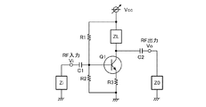
- the RF amplifier 5 is a current feedback type amplifier shown in FIG. 5 or a self-bias type amplifier shown in FIG. 6 in which the gain g hardly fluctuates even if the power supply voltage increases or decreases. Since the current feedback type amplifier and the self-bias type amplifier have known circuit configurations, detailed description thereof will be omitted.
- the magnitude of the gain g is approximately the same as that of the resistor R3 connected to the emitter of the transistor Q1, the impedance circuit ZL connected to the collector of the transistor Q1, and the impedance circuit Z0. It is determined.
- the resistor R4 connected between the collector and the base of the transistor Q2, the resistor R5 connected to the emitter of the transistor Q2, and the collector of the transistor Q2 are connected.
- the magnitude of the gain g is substantially determined by the impedance circuit ZL and the impedance circuit Z0.
- the designer assumes that the active element of the RF amplifier 5 (transistor Q1 in FIG. 5 or transistor Q2 in FIG. 6) comprises a radiator of infinity (thermal resistance 0), and the maximum electrical permissible loss.
- the output voltage of the variable DC power supply 20 shown in FIG. 4B is raised at specific intervals up to the maximum power consumption Pmax [W] in consideration of When the output voltage of 20 is lowered (power is Pmin [W]), the amplitudes of the frequency components of 98 [MHz] measured by the spectrum analyzer 41 are also tabulated and stored in the storage unit 31.
- FIG. 7 is a graph showing the relationship between the power supply voltage of the RF amplifier 5 and the intermodulation distortion level at the specific disturbing wave level stored in the storage unit 31.
- the power supply voltage of the RF amplifier 5 is the reference power supply voltage (8.5 [V])
- the two-wave intermodulation distortion level at the reference RF level I0 is 68 [dB ⁇ V].
- the intermodulation distortion level of the RF amplifier 5 is determined by the above-mentioned intermodulation distortion relative amplitudes in equations (11) and (12). ) Can be calculated.
- log is the common logarithm.
- FIG. 8 is a rewrite of the graph of FIG. 7 with the amount of change in the intermodulation distortion level, where the intermodulation distortion level at the reference power supply voltage is 0 [dB].
- the storage unit 31 stores at least one of the graph of FIG. 7 and the graph of FIG. 8 as the intermodulation distortion-power supply voltage table.
- FIG. 9 is a graph obtained by actually measuring or calculating the power consumption of the RF amplifier 5 at each voltage of the variable DC power supply 20.
- the storage unit 31 stores the graph of FIG. 9 as a power consumption-power supply voltage table.
- the storage unit 31 may store the value of each representative point indicated by a white circle ( ⁇ ) in the graphs of FIGS. 7, 8 and 9, and stores an interpolated curve obtained by interpolating each representative point. You may.
- FIG. 10 is a flowchart showing an example of the operation of the receiving device 1 according to the first embodiment.
- the operation shown in the flowchart of FIG. 10 is started, and when it is shut down, the operation shown in the flowchart of FIG. 10 is terminated. It is assumed that all the interfering waves are within the FM broadcast band (within the reception band).
- step ST1 the control unit 30 controls the output voltage of the variable DC power supply 20 to a predetermined reference power supply voltage (for example, 8.5 [V]).
- the variable DC power supply 20 outputs a reference power supply voltage to the RF amplifier 5 under the control of the control unit 30.
- the power consumption P of the RF amplifier 5 at this time is 0.5 [W] from the power consumption-power supply voltage table of FIG.
- step ST2 the foreground tuner 7 starts measuring the desired wave level DL and outputs the measurement result to the control unit 30.
- the control unit 30 the (center) frequency and the occupied frequency band of the desired wave are known.
- the control unit 30 constantly monitors the desired wave level DL measured by the foreground tuner 7.
- the background tuner 12 constantly scans the reception band, starts measuring the frequency and level of the interfering wave in the reception band, and transmits the measurement result to the control unit 30.
- This background tuner 12 cannot be measured due to the normal saturation of AGC by using an attenuator 11 of about 30 to 40 [dB] as needed, for example, a signal strength (level) of 80 [dB ⁇ V] or more. Also measure.
- step ST4 the control unit 30 refers to the interference wave list generated in step ST3, and when there are two interference waves, it is represented by the above equation (3A), that is, the two waves corresponding to each other in the reception band.
- the frequency of the modulation distortion that is, the frequency of 2 ⁇ - ⁇ and 2 ⁇ - ⁇ is calculated.
- the control unit 30 puts it in all combinations of arbitrary two waves and is represented by the above equation (3A), that is, the intermodulation distortion of the two waves corresponding to the reception band.
- the control unit 30 extracts a combination of three waves that allows up to two waves to overlap (A, A, B). (A, A, C), (A, B, B), (B, B, C), (B, C, C), (C, C, A), (A, A, D), (A) , D, D), (B, B, D), (B, D, D), (C, C, D), (C, D, D).
- IM3 the frequency of the modulation distortion
- the intermodulation distortion in the reception band of each set can be a candidate that can actually cause interference, so that the control unit 30 has 12 two-waves of each other.
- the control unit 30 calculates the frequency of the modulation distortion (IM3).
- the control unit 30 performs three-wave intermodulation for each of the four combinations (A, B, C), (B, C, D), (A, C, D), and (A, B, D).
- IM3 the frequency of distortion
- the frequencies of 24 intermodulation distortions are calculated in total including the two-wave intermodulation distortions.
- step ST5 the control unit 30 determines whether or not there is an intermodulation distortion that matches (exists) in the occupied frequency band of the desired wave among the calculated frequencies of the two-wave or three-wave intermodulation distortion.
- step ST6 the control unit 30 performs the operation shown in step ST6.
- step ST5 “NO” the control unit 30 performs the operation shown in step ST3.
- step ST6 when the control unit 30 has a frequency of intermodulation distortion of two waves or three waves that matches the occupied frequency band of the desired wave, the control unit 30 performs each interference wave for all combinations of the matching interference waves. Calculate the ratio of the level to the reference RF level I0 (that is, the disturbing wave coefficient), calculate the above equation (6) or equation (7), and obtain the IM3 amplitude coefficient M 2 or M 3 of 2 or 3 waves. Ask.
- control unit 30 uses the IM3 amplitude coefficient M 2 or 3 wave IM3 amplitude coefficient M 3 two waves determined, the above equation (11) or formula (12) calculates, RF when the reference power supply voltage
- IM3 level The intermodulation distortion level (hereinafter referred to as IM3 level) of two waves or three waves of the amplifier 5 is obtained.
- the IM3 level of the RF amplifier 5 at the reference power supply voltage is calculated as follows.
- the IM3 level of the two waves having a frequency component of 2 ⁇ - ⁇ is 88 [dB ⁇ V] from the equation (11).
- the IM3 level of the three waves having the frequency component of ⁇ - ⁇ + ⁇ is 74 [dB ⁇ V] from the equation (12).
- control unit 30 calculates the IM3 level of two waves or three waves in the same manner as described above for those combinations. do.
- step ST7 the control unit 30 compares the largest IM3 level among the IM3 levels calculated in step ST6 with the desired wave level DL, and determines whether or not the IM3 level is smaller than the desired wave level DL.
- the process of step ST7 corresponds to a process of determining whether or not the “IM3_DU ratio A” shown in FIG. 1 is 0 or more (DL is a value larger than L1 at the interference wave input level xm).
- step ST7 “YES”) the control unit 30 performs the operation shown in step ST3.
- step ST7 “NO”) the control unit 30 performs the operation shown in step ST8.
- step ST8 the control unit 30 of the RF amplifier 5 required to suppress the IM3 level so that the difference between the IM3 level and the desired wave level DL is 0, or the desired wave level DL is slightly larger.
- the power supply voltage V is read from the intermodulation distortion-power supply voltage table (FIG. 7 or 8) stored in the storage unit 31.
- the power supply voltage V that can be set does not exceed the maximum allowable loss P0 [W] in consideration of the heat dissipation resistance associated with the active element of the RF amplifier 5 and the maximum allowable junction temperature Tjmax of the active element in the steady state. It becomes the setting of. From FIG. 9, P0 [W] is 1.3 [W], and the corresponding power supply voltage value is about 14 [V].
- step ST9 the control unit 30 controls the voltage output from the variable DC power supply 20 to the RF amplifier 5 to the power supply voltage V read from the intermodulation distortion-power supply voltage table in step ST8.
- ⁇ Case 1> For example, when the center frequency of the occupied frequency band of the desired wave is 98.1 [MHz], IM3 having the frequency component of 2 ⁇ - ⁇ (double the frequency of the A wave minus the frequency of the B wave). Matches the occupied frequency band of the desired wave.
- the desired wave level DL 78 [dB ⁇ V]
- DL ⁇ IM3 level that is, (IM3_DU ratio A) ⁇ 0, so that interference between the desired wave and the interfering wave or inversion to the interfering wave occurs. There is a high possibility that it is.
- 88-78 10 [dB].
- the control unit 30 refers to the intermodulation distortion-power supply voltage table stored in the storage unit 31 as shown in the graph of FIG. 8 from the reference level (0 [dB]) to the above 10 [dB].
- Read the power supply voltage V 13 [V] required to reduce.
- the desired wave level DL 95 [dB ⁇ V]
- DL> IM3 level that is, (IM3_DU ratio A)> 0, so that there is no interference between the desired wave and IM3 or inversion to IM3. Therefore, in the flowchart of FIG. 10, the control unit 30 maintains the reference power supply voltage.
- ⁇ Case 2> For example, when the center frequency of the occupied frequency band of the desired wave is 98.8 [MHz], the frequency component of ⁇ - ⁇ + ⁇ (the frequency of the A wave minus the frequency of the B wave and the frequency of the C wave is added) is added.
- the IM3 has the same frequency band as the desired wave.
- a condition satisfying IM3 level> DL + ⁇ L0 may be a condition for raising the power supply voltage of the RF amplifier 5 (step ST7).
- ⁇ L0 is a value larger than 0 and is a value obtained from actual measurement or the like.
- the control unit 30 raises the power supply voltage V when the IM3 level exceeds the desired wave level DL (that is, when the IM3 level ⁇ DL). Not only that, the power supply voltage V may be lowered when the IM3 level falls below the desired wave level DL (that is, when the IM3 level ⁇ DL). By lowering the power supply voltage V, the power consumption of the RF amplifier 5 can be suppressed.
- the power consumption of the RF amplifier 5 is 0.5 as shown in the power consumption-power supply voltage table of FIG. It changes from [W] to 0.3 [W].
- the minimum power supply voltage that can be set is set within a range in which the active element of the RF amplifier 5 does not cut off and can normally perform amplification operation. From FIG. 9, it is about 3 [V].
- control unit 30 considers only the power supply voltage control in the steady operation range of the RF amplifier 5, but dynamically controls the heat generation of the RF amplifier 5 and transiently controls the RF amplifier. Greater loss at 5, i.e. control at higher supply voltage may be taken into account.
- FIGS. 11A, 11B, 12 and 13 specific examples will be described with reference to FIGS. 11A, 11B, 12 and 13.
- FIG. 11A and 11B are flowcharts showing another example of the operation of the receiving device 1 according to the first embodiment. Since the operations of steps ST1 to ST8 shown in FIG. 11A are the same as the operations of steps ST1 to ST8 shown in FIG. 10, the description thereof will be omitted.
- step ST10 the temperature sensor 6 measures the temperature Tsm of the active element (that is, the transistor Q1 shown in FIG. 5 or the transistor Q2 shown in FIG. 6) included in the RF amplifier 5, and controls the measurement result. Output to 30.
- the operation shown in step ST10 may be performed independently of the operation shown in the flowcharts of FIGS. 11A and 11B.
- step ST11 the control unit 30 stores the power consumption P corresponding to the power supply voltage V read from the mutual modulation distortion-power supply voltage table in step ST9 in the storage unit 31, as shown in the graph of FIG. Power consumption-Read from the power supply voltage table.
- step ST12 the control unit 30 controls the variable DC power supply 20 in consideration of the calorific value of the RF amplifier 5, so that the power consumption P [W] is the heat radiation resistance associated with the active element and the heat radiation resistance in the steady state. It is determined whether or not the maximum allowable loss P0 [W] in consideration of the maximum allowable junction temperature Tjmax of the active element is exceeded.
- P ⁇ P0 step ST12 “NO”
- the control unit 30 performs the operation of step ST13.
- P> P0 step ST12 “YES”
- the control unit 30 performs the operation shown in step ST16.
- the RF amplifier 5 consumes a relatively large amount of power to ensure linearity.
- the control unit 30 dynamically controls the power supply voltage V of the RF amplifier 5 required to suppress the intermodulation distortion to a certain level or less, and also copes with the intermodulation distortion level caused by a stronger interfering station. Is desirable.
- the power consumption P [W] of the active element also changes dynamically, but for a short time (for example, the sustainable time t1 described later), the power consumption P [W] is set to a value larger than P0 [W] within a range not exceeding the maximum power consumption Pmax [W] in consideration of the maximum allowable electrical loss of the active element, assuming an infinite radiator. can.
- FIG. 12 is a diagram showing a heat equivalent circuit of an active element included in the RF amplifier 5.
- the total heat capacity including the heat dissipation environment of the active element is W [J / K]
- the total thermal resistance from the semiconductor junction of the active element to the surrounding atmosphere is R [K / W].
- the dependence of the active element consuming P0 on the elapsed time t of the junction temperature Tj can be calculated by the equation (13) using the ambient temperature Ta (Ambient Temperature).
- the temperature Tsm is the temperature of the case surface of the active element measured by the temperature sensor 6.
- t1 is represented by the equation (14), and it is assumed that the Tsm is a value (Tsm ⁇ Tjmax) that is extremely close to the junction temperature Tj of the active element and is lower than the maximum allowable junction temperature Tjmax.
- ln is the natural logarithm.
- the joint temperature Tj does not exceed the maximum allowable joint temperature Tjmax even with the power consumption of the loss P1 [W].
- the power supply voltage V is set to a value at which the power consumption P of the RF amplifier 5 is the minimum operating power Pmin or more. It needs to be set (Pmin ⁇ P2 ⁇ P0).
- the relationship between the power consumption of the RF amplifier 5, the steady saturation temperature, and the sustainable time is shown in FIG.
- step ST16 the control unit 30 calculates the equation (14) to obtain the sustainable time t1 [sec].
- step ST17 the control unit 30 controls the variable DC power supply 20 so that the power supply voltage V read in step ST8 is obtained, and at the same time, starts measuring the elapsed time t.
- step ST18 the control unit 30 compares the largest IM3 level among the IM3 levels calculated in step ST6 with the desired wave level DL, and determines whether or not the IM3 level is larger than the desired wave level DL.
- the control unit 30 performs the operation shown in step ST19.
- the control unit 30 performs the operation shown in step ST20.
- step ST19 when the elapsed time t is longer than the sustainable time t1 (step ST19 “NO”), the control unit 30 performs the operation shown in step ST20.
- step ST19 “YES” when the elapsed time t is equal to or less than the sustainable time t1 (step ST19 “YES”), the control unit 30 performs the operation shown in step ST21.
- step ST20 the control unit 30 forcibly changes the power supply voltage V of the variable DC power supply 20 to a power supply voltage such that P ⁇ P0, and cools the active element.
- step ST21 the control unit 30 is shown in step ST3 when the elapsed time t is longer than the predetermined time td1 (for example, several seconds to several tens of seconds, td1> t1) (step ST21 “NO”). Do the action.
- the control unit 30 can constantly monitor the desired wave level DL.
- the control unit 30 since the IM3 level needs to be calculated one by one by the control unit 30 using the information of the plurality of interfering waves detected by the background tuner 12, the control unit 30 cannot update the value of the IM3 level very frequently. Therefore, when the receiving device 1 is mounted on the mobile body, the signal level of the interfering station changes, so that the IM3 level becomes invalid information immediately.
- control unit 30 forcibly returns to the operation shown in step ST3 when a predetermined time td1 elapses after controlling the power supply voltage V in step ST17 (and step ST13 described later), and newly IM3 level recalculation is performed taking into account the appearing interfering waves.
- the control unit 30 performs the operation shown in step ST18.
- the control unit 30 can calculate the moving distance by using information such as the vehicle speed or GPS (Global Positioning System). In that case, the control unit 30 may compare the travel distance of the receiving device 1 with a predetermined travel distance instead of comparing the elapsed time t with the time td1.
- step ST13 the control unit 30 controls the variable DC power supply 20 so that the power supply voltage V read in step ST8 is obtained, and at the same time, the elapsed time. Start measuring t.
- step ST13 there is no limitation on the sustainable time t1. Since the operations shown in steps ST14 and ST15 are the same as the operations shown in steps ST18 and ST21, the description thereof will be omitted.
- the receiving device 1 includes an antenna 2, an RF amplifier 5, a variable DC power supply 20, a background tuner 12, and a control unit 30.
- the antenna 2 receives at least a predetermined reception band.
- the RF amplifier 5 amplifies the reception band received by the antenna 2.
- the variable DC power supply 20 supplies a power supply voltage to the RF amplifier 5.
- the foreground tuner 7 receives a desired wave existing in the reception band.
- the background tuner 12 detects the frequencies and signal levels of a plurality of interfering waves existing in the reception band.
- the control unit 30 controls the power supply voltage of the RF amplifier 5 supplied by the variable DC power supply 20 based on the information of the plurality of interfering waves detected by the background tuner 12.
- the control unit 30 calculates and calculates the frequency component of the third-order intermodulation distortion caused by the interfering wave frequencies of two or three waves having different frequencies from each other with respect to the third-order nonlinear component generated by the RF amplifier 5.
- the frequency component of the obtained third-order intermodulation distortion is within the occupied frequency band of the desired wave and the calculated third-order intermodulation distortion level is equal to or higher than the signal level of the desired wave
- the extracted third-order intermodulation distortion level is
- the power supply voltage of the RF amplifier 5 is increased so as to be below the signal level of the desired wave.
- the receiving device 1 improved the linearity of the RF amplifier 5 and reduced the third-order intermodulation distortion by raising the power supply voltage while keeping the gain of the RF amplifier 5 constant. As a result, the desired wave was obtained. Can maintain the reception status of.
- the calculated frequency component of the third-order intermodulation distortion is within the occupied frequency band of the desired wave, and the calculated third-order intermodulation distortion level is less than the signal level of the desired wave. If, the power supply voltage of the RF amplifier 5 is reduced within a range in which the calculated third-order intermodulation distortion level does not exceed the signal level of the desired wave. As a result, the receiving device 1 can reduce the power consumption of the RF amplifier 5 while maintaining the reception state of the desired wave.
- the receiving device 1 of the first embodiment includes a storage unit 31.
- the storage unit 31 has a reference third-order intermodulation distortion level measured as a common logarithmic value when two waves having the same reference RF level are simultaneously input to the RF amplifier 5 to which the reference power supply voltage is supplied.
- Modulation distortion-Store s the power supply voltage table.
- the control unit 30 When there are two interfering waves, the control unit 30 normalizes the level of the interfering waves of the two waves at the reference RF level, calculates the interfering wave coefficient of the two waves, and squares the interfering wave coefficient of one of the two waves. Calculate the value obtained by multiplying the value of the common logarithmic wave whose true number is the product of the other interfering wave coefficient by 20, and add the multiplied value by 20 to the reference third-order intermodulation distortion level at the reference power supply voltage. It is defined as the third-order intermodulation distortion level of the two waves under the reference power supply voltage.
- the control unit 30 normalizes the level of the interfering wave of the three waves at the reference RF level, calculates the interfering wave coefficient of the three waves, and determines the interfering wave coefficient of the three waves. Calculate the value obtained by multiplying the value of the common logarithm whose antilogarithm is the value obtained by doubling the product by 20, and add the value obtained by multiplying the product to the reference third-order intermodulation distortion level at the reference power supply voltage to the current three waves. Is defined as the third-order intermodulation distortion level under the reference power supply voltage. As a result, the control unit 30 can calculate the third-order intermodulation distortion level in the actual field corresponding to the reference power supply voltage from the small amount of desktop actual measurement data stored in the storage unit 31.
- control unit 30 of the first embodiment refers to the intermodulation distortion-power supply voltage table stored in the storage unit 31 from the calculation result of the third-order intermodulation distortion level, and is under the current reference power supply voltage.
- the difference in the power supply voltage corresponding to the difference between the third-order intermodulation distortion level and the signal level of the desired wave is obtained, and the power supply voltage of the RF amplifier 5 is controlled based on the difference in the power supply voltage.
- control unit 30 of the first embodiment increases the power supply voltage of the RF amplifier 5, and the power consumption of the RF amplifier 5 corresponding to the increased power supply voltage is included in the RF amplifier 5 in the steady state.
- the value exceeds the maximum permissible loss considering the heat dissipation resistance associated with the active element and the maximum permissible junction temperature of the active element, the thermal time from the current temperature of the active element to the maximum permissible junction temperature is reached.
- the power supply voltage of the RF amplifier 5 is increased by the estimated time (sustainable time t1) based on the constant.
- the control unit 30 By controlling the power of the RF amplifier 5 in consideration of the thermal time constant of the heat dissipation system, the control unit 30 requires a large mutual loss for a relatively short time, which cannot be dealt with by the allowable loss of the active element in the steady state. The modulation distortion can be reduced, and as a result, the deterioration of the reception quality of the desired wave can be avoided.
- control unit 30 of the first embodiment controls the power supply voltage of the RF amplifier 5 based on the signal levels of the plurality of interfering waves detected by the background tuner 12 each time the predetermined time td1 elapses. .. Since the control unit 30 repeatedly monitors the level of the intermodulation distortion and the signal level of the desired wave to control the power supply voltage, the power consumption of the RF amplifier 5 can be suppressed while maintaining the reception quality of the desired wave.
- the receiving device 1 of the first embodiment may be mounted on a mobile body.
- the control unit 30 controls the power supply voltage of the RF amplifier 5 based on the signal levels of the plurality of interfering waves detected by the background tuner 12 each time the moving body moves a predetermined distance. Since the control unit 30 repeatedly monitors the intermodulation distortion level and the signal level of the desired wave to control the power supply voltage, the power consumption of the RF amplifier 5 can be suppressed while maintaining the reception quality of the desired wave.
- Embodiment 2 In the first embodiment, taking the reception of FM broadcasting as an example, the configuration of the receiving device 1 for reducing the intermodulation distortion (IM3) of two waves or three waves with respect to the third-order nonlinear component generated by the RF amplifier 5 has been described.
- intermodulation distortion (IM2) due to second-order nonlinear components such as interference with AM broadcast reception due to FM2 waves, may become a problem. Therefore, in the second embodiment, the configuration of the receiving device 1 that reduces the intermodulation distortion due to the second-order nonlinear component will be described.
- the receiving device 1 may be configured to reduce both the two-wave or three-wave intermodulation distortion due to the third-order linear component and the two-wave intermodulation distortion due to the second-order linear component.
- FIG. 2 Since the configuration of the receiving device 1 according to the second embodiment is the same as the configuration shown in FIG. 2 of the first embodiment on the drawing, FIG. 2 will be referred to below.
- the input signal is represented by the above equation (8)
- the second-order intermodulation distortion (IM2) existing in the output signal is only the sum component and the difference component of the two waves as shown in the above equation (9). be.
- the difference component of the FM2 wave causes interference with AM broadcast reception.
- the receiving device 1 according to the second embodiment will be mainly described as being different from the receiving device 1 according to the first embodiment.
- the designer of the receiving device 1 uses the measurement system shown in FIG. 4B to power the RF amplifier 5 at the IM2 level. Perform a voltage dependency assessment and generate an intermodulation distortion-power supply voltage table.
- the designer stores the generated intermodulation distortion-power supply voltage table (not shown) in the storage unit 31.
- the power supply voltage of the RF amplifier 5 is the reference power supply voltage (8.5 [V])
- the IM2 level at the reference RF level I0 is 80 [dB ⁇ V] from the intermodulation distortion-power supply voltage table (not shown).
- the IM2 level of the RF amplifier 5 at the reference power supply voltage is defined as in the equation (15).
- the designer generates a power consumption-power supply voltage table (not shown) obtained by actually measuring or calculating the power consumption of the RF amplifier 5 at each voltage of the variable DC power supply 20, and stores it in the storage unit 31.
- the receiving device 1 of the second embodiment receives an AM broadcast in Europe
- the receiving device 1 of the second embodiment performs the operations shown in steps ST1, ST2, and ST3 as in the first embodiment.
- the control unit 30 calculates the frequency of the two-wave intermodulation distortion (IM2) according to the equation (9A).
- the control unit 30 calculates the equation (15) to obtain the IM2 level of the two waves at the reference power supply voltage.
- step ST7 the control unit 30 compares the IM2 level with the desired wave level DL and determines whether the IM2 level is smaller than the desired wave level DL.
- the operation after step ST8 is the same as that of the first embodiment.
- the control unit 30 of the second embodiment is the second-order intermodulation distortion caused by the combination of two interfering waves having different frequencies with respect to the second-order nonlinear component generated by the RF amplifier 5.
- the sum component and difference component of the frequencies are calculated, and the frequency component of the calculated second-order intermodulation distortion is within the occupied frequency band of the desired wave, and the calculated second-order intermodulation distortion level is equal to or higher than the signal level of the desired wave.
- the power supply voltage of the RF amplifier 5 is increased so that the extracted second-order intermodulation distortion level is equal to or lower than the signal level of the desired wave.
- the receiving device 1 improved the linearity of the RF amplifier 5 by increasing the power supply voltage while keeping the gain of the RF amplifier 5 constant, and reduced the second-order intermodulation distortion. As a result, the desired wave was obtained. The reception status can be maintained.
- the frequency of the extracted second-order intermodulation distortion is within the occupied frequency band of the desired wave, and the extracted second-order intermodulation distortion level is lower than the signal level of the desired wave.
- the power supply voltage of the RF amplifier 5 is reduced so that the extracted second-order intermodulation distortion level does not exceed the signal level of the desired wave.
- the receiving device 1 can reduce the power consumption of the RF amplifier 5 while maintaining the reception state of the desired wave.
- the receiving device 1 of the second embodiment includes a storage unit 31.
- the storage unit 31 has a reference secondary intermodulation distortion level measured as a value of a common logarithmic when two waves having the same reference RF level are simultaneously input to the RF amplifier 5 to which the reference power supply voltage is supplied.
- Intermodulation including a plurality of second-order intermodulation distortion levels measured as a common logarithmic value when two waves are simultaneously input to an RF amplifier 5 to which a plurality of power supply voltages different from the reference power supply voltage are supplied. Distortion-Remembers the power supply voltage table.
- the control unit 30 normalizes the level of the disturbing waves of the two waves at the reference RF level, calculates the disturbing wave coefficient of the two waves, and sets the value of the common logarithm whose true number is the product of the disturbing wave coefficients of the two waves.
- a value multiplied by 20 is calculated, and the multiplied value is defined as a secondary intermodulation distortion level under the current reference power supply voltage in addition to the reference secondary intermodulation distortion level at the reference power supply voltage.
- the control unit 30 can calculate the second-order intermodulation distortion level in the actual field corresponding to the reference power supply voltage from the small amount of desktop actual measurement data stored in the storage unit 31.
- control unit 30 of the second embodiment refers to the intermodulation distortion-power supply voltage table stored in the storage unit 31 from the calculation result of the secondary intermodulation distortion level, and is under the current reference power supply voltage.
- the difference in the power supply voltage corresponding to the difference between the secondary intermodulation distortion level and the signal level of the desired wave is obtained, and the power supply voltage of the RF amplifier 5 is controlled based on the difference in the power supply voltage.
- Embodiment 3 Compared with the second-order and third-order nonlinear components, the degree of influence on the desired station is significantly smaller, but the intermodulation distortion (that is, IM4, IM5, etc.) due to the fourth-order or higher-order nonlinear components is also second-order. And it can be reduced in the same way as the intermodulation distortion due to the third-order nonlinear component. Since the configuration of the receiving device 1 according to the third embodiment is the same as the configuration shown in FIG. 2 of the first embodiment on the drawing, FIG. 2 will be referred to below.
- nth-order intermodulation distortion due to the nth-order nonlinear component of the RF amplifier 5 intermodulation distortion due to the maximum n-wave including overlap is generated.
- the upper limit of n is set, for example, based on the balance between the effect of reducing intermodulation distortion and the processing load of the control unit 30.
- 2 ⁇ n ⁇ 7, and 2nd to 7th order intermodulation distortions (IM2 to IM7) are targeted.
- the intermodulation distortion is an overlapping combination of n waves excluding the combination of frequencies that are all the same when there is an interfering wave of m waves (m ⁇ n).
- the number of interfering wave combinations to be considered can be calculated from the above equation, but the necessity of applying the frequency of the realistic intermodulation distortion generated from the addition and subtraction of each set of frequencies is determined by the intermodulation by the third-order nonlinear component.
- distortion (IM3) as in the process of deriving the above equations (3A) and (4A), overlapping combinations of (n-1) or less interfering waves other than the same wave are also possible. It is necessary to extract the included sets and calculate the nth-order intermodulation distortion in the reception band from each set.
- Other control methods are in accordance with the first embodiment.
- the frequency of the nth intermodulation distortion (n ⁇ 4) caused by the combination of the plurality of interfering waves detected by the background tuner 12 is the occupied frequency of the desired wave.
- the power supply voltage of the RF amplifier 5 is increased so that the nth-order intermodulation distortion level is equal to or lower than the signal level of the desired wave.
- the receiving device 1 improved the linearity of the RF amplifier 5 and reduced the nth-order intermodulation distortion by increasing the power supply voltage while keeping the gain of the RF amplifier 5 constant. As a result, the desired wave was obtained. The reception status can be maintained.
- the frequency of the nth-order intermodulation distortion (n ⁇ 4) is within the frequency band of the desired wave, and the nth-th order intermodulation distortion level is less than the signal level of the desired wave.
- the power supply voltage of the RF amplifier 5 is reduced within a range in which the nth-order intermodulation distortion level does not exceed the signal level of the desired wave.
- the receiving device 1 can reduce the power consumption of the RF amplifier 5 while maintaining the reception state of the desired wave.
- the present disclosure allows any combination of embodiments, modifications of any component of each embodiment, or omission of any component of each embodiment.
- the receiving device according to the present disclosure is a receiving device for a mobile body including a mobile terminal, a vehicle, a railroad, a ship, an aircraft, etc., and is particularly suitable for being carried into a vehicle or mounted on a vehicle.
- the receiving device takes into consideration the fluctuation of the number of interfering waves, the frequency relationship between the interfering wave and the desired wave, the degree of influence of the interfering wave on the desired wave, the degree of change in the linearity of the RF amplifier, and the like. Since the intermodulation distortion is reduced, it is suitable for use in a receiving device or the like mounted on a moving body.
Landscapes
- Engineering & Computer Science (AREA)
- Computer Networks & Wireless Communication (AREA)
- Signal Processing (AREA)
- Physics & Mathematics (AREA)
- Nonlinear Science (AREA)
- Power Engineering (AREA)
- Noise Elimination (AREA)
- Circuits Of Receivers In General (AREA)
- Superheterodyne Receivers (AREA)
Abstract
制御部(30)は、バックグランドチューナ(12)により検出された複数の妨害波の組み合わせによって引き起こされるn次相互変調歪(n≧2)の周波数が希望波の占有周波数帯域内であり、かつ、n次相互変調歪レベルが希望波の信号レベル以上である場合、n次相互変調歪レベルが希望波の信号レベル以下になるように、RFアンプ(5)の電源電圧を増加させる。
Description
本開示は、受信装置及び制御方法に関するものである。
特許文献1に記載された受信装置は、希望波よりも強い妨害波が存在する際に、高周波(RF:Radio Frequency)用のアンプの直線性を変化させることで、妨害波の影響を低減させていた。
しかしながら、特許文献1に記載された受信装置は、妨害波の数の変動、妨害波と希望波との周波数の関係、妨害波の希望波への影響度合い、及びRFアンプの直線性とゲインの変化度合い等に関して考慮されたものではない。そのため、希望波と周波数が近い複数の妨害波により生じる相互変調歪を低減するために、特許文献1記載の装置によりRFアンプの直線性を変化させるため、バイアス電流を変化させると、RFアンプのゲインが変化してしまう可能性があり、その結果、希望波の受信状態が変化してしまう可能性があるという課題があった。
本開示は、上記のような課題を解決するためになされたもので、相互変調歪を低減する際にRFアンプのゲインを一定に保ち、希望波の受信状態を維持することを目的とする。
本開示に係る受信装置は、少なくとも予め定められた受信帯域を受信するアンテナと、アンテナが受信した受信帯域を増幅するRFアンプと、RFアンプへ電源電圧を供給する可変直流電源と、受信帯域内に存在する希望波を受信するフォアグランドチューナと、受信帯域内に存在する複数の妨害波の周波数と信号レベルを検出するバックグランドチューナと、バックグランドチューナにより検出された複数の妨害波の信号レベルに基づいて、可変直流電源が供給するRFアンプの電源電圧を制御する制御部とを備え、制御部は、バックグランドチューナにより検出された複数の妨害波の組み合わせによって引き起こされるn次相互変調歪(n≧2)の周波数がフォアグランドチューナにより受信された希望波の占有周波数帯域内であり、かつ、n次相互変調歪レベルが希望波の信号レベル以上である場合、n次相互変調歪レベルが希望波の信号レベル以下になるように、RFアンプの電源電圧を増加させるものである。
本開示によれば、RFアンプの電源電圧を上げることによりRFアンプの直線性を改善して相互変調歪を低減するようにしたので、RFアンプのゲインを一定に保つことができ、結果として希望波の受信状態を維持できる。
以下、本開示をより詳細に説明するために、本開示を実施するための形態について、添付の図面に従って説明する。
実施の形態1.
図1は、一般的なRFアンプの入出力特性を示すグラフである。まず、図1を参照して、本開示の概念を説明する。図1のグラフは、RFアンプに固定の希望波と複数の妨害波(ここでは2波)とが入力され、当該複数の妨害波の入力レベル(以下、「レベル」を「振幅」とも言うが、いずれも電圧振幅のことである)が変化した場合の、RFアンプの出力を表している。この図1のグラフの縦軸(出力)及び横軸(入力)がともに対数(dB)で表されている。この図1のグラフから、以下の(A)~(D)が読み取れる。
実施の形態1.
図1は、一般的なRFアンプの入出力特性を示すグラフである。まず、図1を参照して、本開示の概念を説明する。図1のグラフは、RFアンプに固定の希望波と複数の妨害波(ここでは2波)とが入力され、当該複数の妨害波の入力レベル(以下、「レベル」を「振幅」とも言うが、いずれも電圧振幅のことである)が変化した場合の、RFアンプの出力を表している。この図1のグラフの縦軸(出力)及び横軸(入力)がともに対数(dB)で表されている。この図1のグラフから、以下の(A)~(D)が読み取れる。
(A)Lcは、希望波のRF出力レベルであり、一定値の希望波レベルDL(Desired Level)[dBμV]を持つとする。入力レベル換算では、Lcは、DL-g[dBμV]となる。gは、RFアンプのリニア(線形)ゲインである。
(B)L0は、傾き1のRFアンプのリニア入出力特性であり、妨害波入力に対するリニア出力を表している。L0と縦軸との交点は上記gであり、計算又は図4Aに示されるリニアゲインの測定系を用いた入出力レベルの実測により求められる。図4Aにおいて、シグナルジェネレータ40は、例えば、98[MHz]の信号を生成してRFアンプ5へ出力する。その際、可変直流電源20がRFアンプ5へ出力する電圧は、予め定められた基準電源電圧の値で固定とする。スペクトラムアナライザ41は、98[MHz]の周波数成分の大きさを測定する。
上記L0は、妨害波のRF入力レベルxに対するRFアンプのリニア出力(妨害波の基本波出力)の追従性と考えられ、次式で表される。なお、RFアンプのゲインgは、電源電圧が変化してもほとんど変化しない。つまり、ゲインgは、電源電圧依存性を持たない。
L0:F0(x)=x+g[dB]
L0:F0(x)=x+g[dB]
(C)L1は、ある基準電源電圧(例えば、8.5[V])での3次非線形出力のうち、複数妨害波による相互変調歪(IM3)の入出力依存性を表す。当該L1は、入力の3乗に比例して増加するために傾きは3となり、リニア出力L0とはx=x1において仮想的な点IP3a(IP:Intercept Point)で交わる。
ここで、L1の相互変調歪(IM3)のレベルと希望波レベルDLとのレベル差は、「IM3_DU比A」(DU:Desired to Undesired)で表される。IM3の周波数が希望波の周波数と一致する場合、RFアンプが良好な希望波受信を維持するために、「IM3_DU比A」は0以上でなければならない。換言すれば、DL≧IM3レベルでなければならない。
また、L1と縦軸との交点は、基準電源電圧時のRFアンプの相互変調歪ゲインb1であり、当該L1は次式で表される。
L1:f1(x)=3x+b1
L1:f1(x)=3x+b1
RF入力レベルx=x0における妨害波基本波と相互変調歪との差異をCN(Carrier to Noise)[dB]とすると、x1とb1は次式で与えられる。なお、CNとb1は、電源電圧依存性を持つ。
x1=x0+CN/2[dBμV]
b1=-2x0+g-CN[dB]
x1=x0+CN/2[dBμV]
b1=-2x0+g-CN[dB]
(D)L2は、基準電源電圧から電圧を上げた場合の相互変調歪(IM3)の入出力振幅依存特性を表す。例えば、電源電圧を基準電源電圧8.5[V]から12[V]へ上げた場合、RFアンプのリニアリティ(直線性)が改善されるので、L1がグラフ右側へシフトし、同一妨害波入力レベルに対するIM3の大きさは「IM3_ΔDU比B」分だけ低下する。当該L2は、リニア出力L0とはx=x2において仮想的な点IP3bで交わる。
ここで、L2の相互変調歪と希望波レベルDLとのレベル差は、「(IM3_DU比A)+(IM3_ΔDU比B)」で表され、L1の相互変調歪と希望波レベルDLとのレベル差と比較して大きくなる。
また、L2と縦軸との交点は、基準電源電圧から増加した後の電源電圧(例えば、12[V])時のRFアンプの相互変調歪ゲインb2であり、当該L2は次式で表される。
L2:f2(x)=3x+b2
L2:f2(x)=3x+b2
RF入力レベルx=x0における妨害波基本波と相互変調歪との差異CNは、L1からの改善度合いをΔCN[dB]とすると、CN+ΔCN[dB]となる。x2とb2は次式で与えられる。
x2=x0+(CN+ΔCN)/2[dBμV]
b2=-2x0+g-(CN+ΔCN)[dB]
x2=x0+(CN+ΔCN)/2[dBμV]
b2=-2x0+g-(CN+ΔCN)[dB]
また、IP3aからIP3bへの妨害波入力レベル改善度合いは、次式で表される。
Δx=x2-x1=ΔCN/2[dB]
ΔCN=b2-b1[dB]
Δx=x2-x1=ΔCN/2[dB]
ΔCN=b2-b1[dB]
次に、RFアンプの3次非線形成分による相互変調歪(IM3)と高調波歪について説明する。3次非線形成分は重複も含めた3個の周波数成分の加減算から求められる。
それぞれω1、ω2、ω3の角周波数を持つ3つの妨害波の合成波Vを、非線形回路に入力する場合を考える。基準RFレベルをI0[dBμV]とし、この値でそれぞれの妨害波の振幅を規格化した値を、それぞれ、妨害波係数u、v、wとする。合成波Vが式(1)で表される場合、3次非線形性成分V3は式(2)で表される。
それぞれω1、ω2、ω3の角周波数を持つ3つの妨害波の合成波Vを、非線形回路に入力する場合を考える。基準RFレベルをI0[dBμV]とし、この値でそれぞれの妨害波の振幅を規格化した値を、それぞれ、妨害波係数u、v、wとする。合成波Vが式(1)で表される場合、3次非線形性成分V3は式(2)で表される。

2波α、βによる相互変調歪を各周波数成分に分解すると、式(3-1)及び式(3-2)で表される4つの周波数成分となる。(β,γ)、(γ,α)の組合せも考えると、相互変調歪としては計12個の周波数成分が存在する。ここで、ω1、ω2、ω3が全てあるラジオ受信帯域内に存在する角周波数と仮定する。あるラジオ受信帯域とは、「予め定められた受信帯域」に相当し、例えば欧州のFM放送であれは87.5~108[MHz]である。ラジオ受信帯域の下端周波数をBmin、上端周波数をBmaxとすると、3Bmin≧Bmaxであれば、式(3-1)の2α+β、式(3-2)の2β+α等の相互変調歪の周波数は、ラジオ受信帯域外となる。一方、式(3-1)の2α-β、式(3-2)の2β-α等の、式(3A)で示される6つの周波数成分のいずれかが、希望波の信号レベル以上で希望波の占有周波数帯域内に存在すると、混信、または受信品質劣化の原因となる。希望波の占有周波数帯域は、例えば欧州のFM放送であれば数十[kHz]、AM放送であれば数[kHz]である。

3波の場合、相互変調歪を各周波数成分に分解すると、式(4)となる。相互変調歪としては計4個の周波数成分が存在する。2波の場合と同様に、3波の場合も、ω1、ω2、ω3が同一のラジオ受信帯域内に存在し、かつ、3Bmin≧Bmaxであれば、α+β+γの相互変調歪の周波数は、ラジオ受信帯域外となる。一方、式(4A)で示される3つの周波数成分のうちのいずれかが、希望波の信号レベル以上で希望波の占有周波数帯域内に存在すると、混信、または受信品質劣化の原因となる。また、式(4A)で正符号の2波が同一波である場合、式(3A)のいずれかの値と等しくなる。

式(2)から、2波によるIM3の振幅は、3u2v、3uv2、3u2w、3v2w、3uw2、3vw2であり、3波によるIM3の振幅は6uvwである。ここで、妨害2波のIM3相対振幅は式(6)で表され、M2を2波IM3振幅係数と定義する。同様に、妨害3波のIM3相対振幅は式(7)で表され、M3を3波IM3振幅係数と定義する。妨害2波のIM3相対振幅は、2波IM3振幅係数の3倍になるのに対し、妨害3波のIM3相対振幅は、3波IM3振幅係数の6倍になることが分かる。IM3振幅係数を同一とした場合、妨害3波のIM3相対振幅は、妨害2波のIM3相対振幅の2倍となる。4波以上の3次非線形成分による相互変調歪は存在しない。
(妨害2波のIM3相対振幅)
=3M2
=3u2v、3uv2、3u2w、3v2w、3uw2、3vw2 …(6)
(妨害3波のIM3相対振幅)
=6M3
=6uvw …(7)
次に、RFアンプの2次非線形成分による相互変調歪(IM2)と高調波歪について説明する。2次非線形成分は重複も含めた2個の周波数成分の加減算から求められる。
それぞれω4、ω5の角周波数を持つ2つの妨害波の合成波Vを、非線形回路に入力する場合を考える。基準RFレベルをI0[dBμV]とし、この値でそれぞれの妨害波の振幅を規格化した値を、妨害波係数x、yとする。合成波Vが式(8)で表される場合、2次非線形成分V2は式(9)で表される。
それぞれω4、ω5の角周波数を持つ2つの妨害波の合成波Vを、非線形回路に入力する場合を考える。基準RFレベルをI0[dBμV]とし、この値でそれぞれの妨害波の振幅を規格化した値を、妨害波係数x、yとする。合成波Vが式(8)で表される場合、2次非線形成分V2は式(9)で表される。

ここで、ω4、ω5があるラジオ受信帯域内(例えば、欧州のFM放送の87.5~108[MHz])に存在すると、両者の差分の相互変調歪の周波数が別のラジオ受信帯域内(例えば、欧州のAM放送の531~1602[kHz])に存在することになる。この場合、δ+εの相互変調歪の周波数は、AM放送の受信帯域外となる。一方、式(9A)で示されるδ-εの周波数が、希望波の信号レベル以上で希望波の占有周波数帯域内に存在すると、混信、または受信品質劣化の原因となる。
式(9)から、IM2相対振幅は式(10)で表され、M22は2波IM2振幅係数と定義される。3波以上の2次非線形成分による相互変調歪は存在しない。
(IM2相対振幅)=2M22=2xy …(10)
次に、実施の形態1に係る受信装置1についてFM放送の受信を例にとり、説明する。実施の形態1に係る受信装置1は、2波の3次相互変調歪又は3波の3次相互変調歪の少なくとも一方を低減する構成とする。
図2は、実施の形態1に係る受信装置1の構成例を示すブロック図である。受信装置1は、アンテナ2、バンドパスフィルタ3、分配器4、RFアンプ5、温度センサ6、フォアグランドチューナ7、オーディオ処理部8、スピーカ9、ノッチフィルタ10、減衰器11、バックグランドチューナ12、可変直流電源20、制御部30、記憶部31、及び操作部32を備える。
バンドパスフィルタ3は、アンテナ2が受信する電波のうち、必要な受信帯域のみを通過させるフィルタである。分配器4は、バンドパスフィルタ3からRFアンプ5へのRFパスと、バンドパスフィルタ3からノッチフィルタ10へのRFパスとを分岐させる。
RFアンプ5は、高周波用のアンプである。このRFアンプ5は、図1のグラフに示される入出力特性を持つ。可変直流電源20は、後述する制御部30によってRFアンプ5へ出力する電圧を可変できる電源である。この可変直流電源20は、昇降圧型DCDCコンバータ、降圧型DCDCコンバータ、又はシリーズレギュレータ等である。温度センサ6は、RFアンプ5に含まれる能動素子(トランジスタ等)の温度を測定する。
フォアグランドチューナ7は、希望波(希望局)を受信し、かつ希望波の信号強度を測定する。オーディオ処理部8は、フォアグランドチューナ7が出力する信号を復調処理等し、処理後の信号を増幅する。スピーカ9は、オーディオ処理部8が増幅した信号を再生する。
ノッチフィルタ10は、後述する制御部30が指示する希望波の周波数成分を除去するフィルタである。このノッチフィルタ10は、希望波の信号がバックグランドチューナ12側に給電されて減衰されるのを防ぐ。減衰器11は、バックグランドチューナ12のAGC(Auto Gain Control)が飽和して信号強度が正確に測定できなくなった場合に制御部30からの指示を受けて、RF信号を減衰させてAGCの飽和を解き、バックグランドチューナ12に正確な信号強度測定を行わせる。減衰器11は、抵抗器等の受動素子で構成される。バックグランドチューナ12は、希望波以外の周波数をスキャンし、希望放送局以外の信号強度を測定する。
制御部30は、フォアグランドチューナ7が測定する希望波の信号強度、及びバックグランドチューナ12が測定する希望波以外の信号強度を元に、各種の演算を行う。制御部30が行う演算内容については後述する。記憶部31は、制御部30が演算に用いる各種情報、及び制御部30が行った演算結果を記憶する。操作部32は、受信装置1をユーザが操作するためのユーザインタフェースである。操作部32は、スイッチ、リモートコントローラ、又はタッチディスプレイ等である。
図3は、実施の形態1に係る受信装置1の制御部30と記憶部31のハードウェア構成例を示すブロック図である。受信装置1における記憶部31の機能は、メモリ102により実現される。また、受信装置1における制御部30の機能は、処理回路により実現される。即ち、受信装置1は、制御部30の機能を実現するための処理回路を備える。処理回路は、メモリ102に格納されるプログラムを実行するプロセッサ101により実現される。この制御部30の機能は、ソフトウェア、ファームウェア、又はソフトウェアとファームウェアとの組み合わせにより実現される。ソフトウェア又はファームウェアはプログラムとして記述され、メモリ102に格納される。プロセッサ101は、メモリ102に格納されたプログラムを読みだして実行することにより、制御部30の機能を実現する。即ち、受信装置1は、プロセッサ101により実行されるときに、後述する図10等のフローチャートで示されるステップが結果的に実行されることになるプログラムを格納するためのメモリ102を備える。また、このプログラムは、制御部30の手順又は方法をコンピュータに実行させるものであるとも言える。
ここで、プロセッサ101とは、CPU(Central Processing Unit)、処理装置、演算装置、マイクロプロセッサ、又はDSP(Digital Signal Processor)等のことである。
メモリ102は、前記プログラムを格納するEPROM(Erasable Programmable ROM)、又はフラッシュメモリ等の不揮発性メモリと、プロセッサ101の処理及び演算で用いるRAM(Random Access Memory)等の揮発性メモリとで構成される。
メモリ102は、前記プログラムを格納するEPROM(Erasable Programmable ROM)、又はフラッシュメモリ等の不揮発性メモリと、プロセッサ101の処理及び演算で用いるRAM(Random Access Memory)等の揮発性メモリとで構成される。
次に、RFアンプ5で発生する3次の非線形成分について、2波又は3波の強入力妨害波に起因する、希望波の占有周波数帯域内の3次相互変調歪(IM3)を低減するための制御部30の実施手順を述べる。当該3次相互変調歪は、実フィールドで妨害波の希望波への混信又は妨害波への反転等の問題を引き起こし、良好な希望波受信を阻害する。
まず、事前の机上測定として、受信装置1の設計者は、図4Bに示される測定系を用いて、RFアンプ5のIM3レベルの電源電圧依存性評価を行い、相互変調歪―電源電圧テーブルを生成する。この測定で用いた入力RFレベルの値を基準として、実フィールドでの妨害波レベルと相対比較することにより、RFアンプ5で発生するIM3レベルの算出を行う。図4Bは、RFアンプ5の3次相互変調歪レベルの測定系を示す図である。一例として、シグナルジェネレータ42は、基準RFレベルI0を110[dBμV](316[mV])とし周波数を99[MHz]とした妨害波UD1を生成してミキサ44へ出力する。シグナルジェネレータ43は、基準RFレベルI0を110[dBμV](316[mV])とし周波数を100[MHz]とした妨害波UD2を生成してミキサ44へ出力する。ミキサ44は、妨害波UD1と妨害波UD2とを合成した合成波を、RFアンプ5に入力する。つまり、式(1)において、u=1、v=1、w=0、及び合成時の信号損失を0とした合成波VがRFアンプ5に入力される。可変直流電源20の電圧は、基準電源電圧8.5[V]である。スペクトラムアナライザ41は、このときの3次非線形成分による2波相互変調歪の周波数成分の大きさ、例えば2×(UD1の周波数)-(UD2の周波数)=98[MHz]の大きさを測定する。2×(UD1の周波数)-(UD2の周波数)は、式(3A)の2α-β等に相当する。設計者は、スペクトラムアナライザ41が測定した周波数成分の大きさを、RFアンプ5の電源電圧を変化させて測定し、測定結果を相互変調歪―電源電圧テーブルとして記憶部31に記憶する。
なお、RFアンプ5は、電源電圧が増減してもゲインgがほぼ変動しない、図5に示される電流帰還型アンプ又は図6に示される自己バイアス型アンプである。当該電流帰還型アンプ及び自己バイアス型アンプは、公知の回路構成であるため、詳細な説明は省略する。図5に示される電流帰還型アンプにおいては、トランジスタQ1のエミッタに接続された抵抗器R3と当該トランジスタQ1のコレクタに接続されたインピーダンス回路ZLとインピーダンス回路Z0とで、ほぼゲインgの大きさが決定される。図6に示される自己バイアス型アンプにおいては、トランジスタQ2のコレクタ-ベース間に接続された抵抗器R4と、当該トランジスタQ2のエミッタに接続された抵抗器R5と、当該トランジスタQ2のコレクタに接続されたインピーダンス回路ZLとインピーダンス回路Z0とで、ほぼゲインgの大きさが決定される。
続いて、設計者は、RFアンプ5の能動素子(図5におけるトランジスタQ1、又は図6におけるトランジスタQ2)が無限大(熱抵抗0)の放熱器を備えると仮定し、かつ電気的最大許容損失を考慮した最大消費電力Pmax[W]まで、図4Bに示される可変直流電源20の出力電圧を特定間隔で上げた場合、及び当該能動素子がカットオフする直前の動作可能最低電圧まで可変直流電源20の出力電圧を下げた場合(電力をPmin[W]とする)の、スペクトラムアナライザ41が測定する98[MHz]の周波数成分の振幅も、それぞれ、テーブル化して記憶部31に記憶する。
図7は、記憶部31が記憶する、特定妨害波レベルでのRFアンプ5の電源電圧と相互変調歪レベルとの関係を示すグラフである。図7の例では、RFアンプ5の電源電圧が基準電源電圧(8.5[V])であるときの、基準RFレベルI0における2波相互変調歪レベルは、68[dBμV]である。基準電源電圧で任意レベルの2波又は3波の妨害波が印加されたとき、RFアンプ5の相互変調歪レベルは、上述した相互変調歪相対振幅を用いて、式(11)と式(12)により計算可能である。logは、常用対数である。
(2波相互変調歪レベル)
=68+20log(M2)[dBμV] …(11)
(3波相互変調歪レベル)
=68+20log(2M3)
=68+20{log(M3)+log2}[dBμV] …(12)
図8は、基準電源電圧での相互変調歪レベルを0[dB]として、相互変調歪レベルの変化量で図7のグラフを書き直したものである。記憶部31は、図7のグラフ又は図8のグラフの少なくとも一方を、上記相互変調歪―電源電圧テーブルとして記憶する。
図9は、可変直流電源20の各電圧におけるRFアンプ5の消費電力を実測又は計算したグラフである。記憶部31は、図9のグラフを、消費電力―電源電圧テーブルとして記憶する。なお、記憶部31は、図7、図8、及び図9のグラフにおいて、白丸(〇)で示される各代表点の値を記憶してもよいし、各代表点を補間した補間曲線を記憶してもよい。
次に、受信装置1が欧州のFM放送を受信する事例を、図10のフローチャートを用いて説明する。図10は、実施の形態1に係る受信装置1の動作の一例を示すフローチャートである。受信装置1は、例えば、起動すると図10のフローチャートに示される動作を開始し、シャットダウンすると図10のフローチャートに示される動作を終了する。妨害波は全てFM放送帯域内(受信帯域内)に存在すると仮定する。
ステップST1において、制御部30は、可変直流電源20の出力電圧を、予め定められた基準電源電圧(例えば、8.5[V])に制御する。可変直流電源20は、制御部30の制御に従い、基準電源電圧をRFアンプ5へ出力する。ちなみに、このときのRFアンプ5の消費電力Pは、図9の消費電力―電源電圧テーブルより0.5[W]である。
ステップST2において、フォアグランドチューナ7は、希望波レベルDLの測定を開始し、測定結果を制御部30へ出力する。制御部30において、希望波の(中心)周波数及び占有周波数帯域は既知である。制御部30は、フォアグランドチューナ7が測定する希望波レベルDLを常にモニタする。
ステップST3において、バックグランドチューナ12は、受信帯域内を常時スキャンし、受信帯域内の妨害波の周波数とレベルの測定を開始し、測定結果を制御部30へ送信する。このバックグランドチューナ12は、30~40[dB]程度の減衰器11を必要に応じて使用することにより、AGCが通常飽和することによって測定できない、例えば80[dBμV]以上の信号強度(レベル)も測定する。
ステップST4において、制御部30は、ステップST3で生成した妨害波リストを参照し、妨害波が2波ある場合、上記式(3A)で表される、すなわち受信帯域内に該当する2波の相互変調歪の周波数、すなわち2α―β及び2β―αの周波数を演算する。一方、妨害波が3波以上ある場合、制御部30は、任意2波の全ての組合せに置いて、上式(3A)で表される、すなわち受信帯域内に該当する2波の相互変調歪の周波数を演算すると共に、任意3波の全ての組合せに置いて、上式(4A)で表される、すなわち受信帯域内に該当する3波の相互変調歪の周波数、すなわちα―β+γ、―α+β+γ及びα+β―γの周波数を演算する。
例えば、受信帯域内に4波の妨害波A、B、C、Dがある場合、制御部30は、2波重複までを許した3波の組合せを抽出すると、(A,A,B)、(A,A,C)、(A,B,B)、(B,B,C)、(B,C,C)、(C,C,A)、(A,A,D)、(A,D,D)、(B,B,D)、(B,D,D)、(C,C,D)、(C,D,D)となり、これら12個の各組み合わせについて、2波相互変調歪(IM3)の周波数を演算する。上式(3A)によると、これらの各妨害波の組合せにおいて、各組1つの受信帯域内相互変調歪が現実に妨害を与えうる候補となりうるので、制御部30は、12個の2波相互変調歪(IM3)の周波数を計算する。また、制御部30は、(A,B,C)、(B,C,D)、(A,C,D)、(A,B,D)の4個の各組み合わせについて、3波相互変調歪(IM3)の周波数を演算する。上式(4A)によると、これらの各組合せにおいて、それぞれ3つの受信帯域内相互変調歪が現実に妨害を与えうる候補となりうるので、4×3=12個の3波相互変調歪(IM3)の周波数が計算され、2波相互変調歪の分も合わせると計24個の相互変調歪(IM3)の周波数が計算される。
一般に、m波の妨害波が存在する場合、n(m≧n)次相互変調歪(IMn)を生成する妨害波の組み合わせは、全て同一波(n重複)となる妨害波の組み合わせを除くn波の重複組み合わせとなる。そのため、制御部30は、mHn-m=m+n-1Cn-m種類の妨害波の組み合わせについて考慮が必要である。これによって、例えば上記3次相互変調歪(IM3)を妨害波が4波の場合について再度計算してみると、全て同一となる周波数の組み合わせ(4通り)を除く、3波の重複組み合わせとなるため、6C3-4=20-4=16種類の組合せについて考慮が必要となる。2波による相互変調歪(IM3)については、上式(3A)より各組み合せで1つの相互変調歪の周波数しか発生しないが、3波による相互変調歪(IM3)については、(A,B,C)、(B,C,D)、(A,C,D)、(A,B,D)の各組で、それぞれ3つの相互変調歪の周波数が発生するので、既に計算された1つを差し引き、(3-1)×4=8を前記16種類に加えた24種の相互変調歪の周波数が発生することになり、前記計算結果と一致する。
考慮すべき妨害波の組合せ数については、上式より計算できるが、各組の周波数の加減算から生成される現実的な相互変調歪の周波数の適用要否については、3次非線形成分による相互変調歪(IM3)の場合に、上式(3A)及び上式(4A)導出過程にて行ったのと同様に、全て同一波以外の、(n-1)個以下の妨害波の重複組み合わせも含めた組を抽出し、各組からn次の受信帯域内相互変調歪をそれぞれ計算する必要がある。
ステップST5において、制御部30は、算出された2波又は3波の相互変調歪の周波数のうち、希望波の占有周波数帯域に一致(存在)する相互変調歪があるか否かを判定する。希望波の周波数帯域に一致する周波数の相互変調歪がある場合(ステップST5“YES”)、制御部30は、ステップST6に示される動作を行う。希望波の周波数帯域に一致する周波数の相互変調歪がない場合(ステップST5“NO”)、制御部30は、ステップST3に示される動作を行う。
ステップST6において、制御部30は、2波又は3波の相互変調歪の周波数のうち、希望波の占有周波数帯域に一致するものがある場合、一致する妨害波の全ての組み合わせについて、各妨害波のレベルの基準RFレベルI0に対する比率(つまり、上記妨害波係数)を計算し、上式(6)又は式(7)を計算して2波又は3波のIM3振幅係数M2又はM3を求める。そして、制御部30は、求めた2波のIM3振幅係数M2又は3波のIM3振幅係数M3を用いて、上式(11)又は式(12)を計算し、基準電源電圧時におけるRFアンプ5の2波又は3波の相互変調歪レベル(以下、IM3レベルと称する)を求める。
例えば、上記妨害波(A,B,C)の組み合わせに関して、以下のように仮定する。
<A波>
120[dBμV](1000[mV])
ω1t=α
ω1t/2π=98.3[MHz]
<B波>
110[dBμV](316[mV])
ω2t=β
ω2t/2π=98.5[MHz]
<C波>
100[dBμV](100[mV])
ω3t=γ
ω3t/2π=99.0[MHz]
<A波>
120[dBμV](1000[mV])
ω1t=α
ω1t/2π=98.3[MHz]
<B波>
110[dBμV](316[mV])
ω2t=β
ω2t/2π=98.5[MHz]
<C波>
100[dBμV](100[mV])
ω3t=γ
ω3t/2π=99.0[MHz]
基準RFレベルI0=110[dBμV](316[mV])とすると、妨害波係数u=1000/316=3.16、妨害波係数v=316/316=1、妨害波係数w=100/316=0.316となる。このとき、基準電源電圧でのRFアンプ5のIM3レベルは、以下のように計算される。
2α-βの周波数成分を持つ2波のIM3レベルは、式(11)より、88[dBμV]となる。
(2波相互変調歪レベル)
=68+20log(M2)=68+20log(u2v)
=68+40log(u)+20log(v)
=68+20+0=88[dBμV]
(2波相互変調歪レベル)
=68+20log(M2)=68+20log(u2v)
=68+40log(u)+20log(v)
=68+20+0=88[dBμV]
α-β+γの周波数成分を持つ3波のIM3レベルは、式(12)より、74[dBμV]となる。
(3波相互変調歪レベル)
=68+20{log(M3)+log2}
=68+20log(u)+20log(v)+20log(w)+6
=68+10+0-10+6=74[dBμV]
(3波相互変調歪レベル)
=68+20{log(M3)+log2}
=68+20log(u)+20log(v)+20log(w)+6
=68+10+0-10+6=74[dBμV]
さらに、制御部30は、(A,B,C)以外の組み合わせでも希望波の占有周波数帯域に一致するものがある場合、それらの組み合わせについても上記同様に2波又は3波のIM3レベルを演算する。
ステップST7において、制御部30は、ステップST6で演算したIM3レベルのうちの最も大きいIM3レベルと希望波レベルDLとを比較し、IM3レベルが希望波レベルDLより小さいか否かを判定する。ステップST7の処理は、図1に示される「IM3_DU比A」が0以上である(妨害波入力レベルxmにおいて、DLがL1より大きい値である)か否かを判定する処理に相当する。IM3レベルが希望波レベルDLよりも小さい場合(ステップST7“YES”)、制御部30は、ステップST3に示される動作を行う。IM3レベルが希望波レベルDL以上である場合(ステップST7“NO”)、制御部30は、ステップST8に示される動作を行う。
ステップST8において、制御部30は、IM3レベルと希望波レベルDLとの差異が0、又は希望波レベルDLの方がやや大きくなるように、IM3レベルを抑圧するために必要な、RFアンプ5の電源電圧Vを、記憶部31に記憶されている相互変調歪―電源電圧テーブル(図7または図8)から読み取る。ただし、設定できる電源電圧Vは、RFアンプ5の能動素子に付随する放熱抵抗と、定常状態における能動素子の最大許容接合部温度Tjmaxとを考慮した最大許容損失P0[W]を超えない範囲での設定となる。図9からP0[W]は1.3[W]でそれに相当する電源電圧の値は約14[V]となる。
ステップST9において、制御部30は、可変直流電源20からRFアンプ5へ出力する電圧を、ステップST8で相互変調歪―電源電圧テーブルから読み取った電源電圧Vに制御する。
<事例1>
例えば、希望波の占有周波数帯域の中心周波数が98.1[MHz]である場合、前記2α-β(2倍のA波の周波数からB波の周波数を引いたもの)の周波数成分を持つIM3が上記希望波の占有周波数帯域に一致する。ここで、希望波レベルDL=78[dBμV]であれば、DL<IM3レベル、すなわち(IM3_DU比A)<0であるので、希望波と妨害波との混信又は妨害波への反転が発生している可能性が高い。DL≧IM3レベルとするには、88-78=10[dB]のIM3レベルの低減が必要である。そのため、制御部30は、記憶部31に記憶されている、図8のグラフで示されるような相互変調歪―電源電圧テーブルを参照し、リファレンスレベル(0[dB])から上記10[dB]の低減に必要な電源電圧V=13[V]を読み取る。
一方、希望波レベルDL=95[dBμV]である場合、DL>IM3レベル、すなわち(IM3_DU比A)>0であるので、希望波とIM3との混信又はIM3への反転はしていない。そのため、図10のフローチャートにおいては、制御部30は、基準電源電圧を維持する。
<事例2>
例えば、希望波の占有周波数帯域の中心周波数が98.8[MHz]である場合、α-β+γ(A波の周波数からB波の周波数を引きC波の周波数を加えたもの)の周波数成分を持つIM3が上記希望波の周波数帯域に一致する。ここで、希望波レベルDL=70[dBμV]であれば、DL≧IM3レベルとするには、74-70=4[dB]のIM3レベルの低減が必要である。そのため、制御部30は、記憶部31に記憶されている、図8のグラフで示されるような相互変調歪―電源電圧テーブルを参照し、上記4[dB]の低減に必要な電源電圧V=10[V]を読み取る。
一方、希望波レベルDL=95[dBμV]である場合、DL>IM3レベル、すなわち(IM3_DU比A)>0であるので、希望波とIM3との混信又はIM3への反転はしていない。そのため、図10のフローチャートにおいては、制御部30は、基準電源電圧を維持する。
なお、FM放送では、キャプチャーレシオに依存するが、過渡的な状態ではIM3レベルが希望波レベルDLを上回ってもすぐに混信又は反転が発生しない場合が多い。そのため、FM放送では、IM3レベル>DL+ΔL0を満足する条件を、RFアンプ5の電源電圧を上げる条件としてもよい(ステップST7)。ここで、ΔL0は、0より大きい値であって、実測等から求めた値である。
また、図10のフローチャートに示されるステップST7、ST8では、制御部30は、IM3レベルが希望波レベルDLを上回った場合(つまり、IM3レベル≧DLである場合)に電源電圧Vを上げたが、それだけでなく、IM3レベルが希望波レベルDLを下回った場合(つまり、IM3レベル<DLである場合)に電源電圧Vを下げてもよい。電源電圧Vを下げることで、RFアンプ5の消費電力を抑制できる。
上記<事例1>において、希望波レベルDL=95[dBμV]である場合、DL>IM3レベル、すなわち(IM3_DU比A)>0であるので、希望波とIM3との混信又はIM3への反転はしていない。この場合、制御部30は、RFアンプ5の電源電圧を下げて消費電力を低減するために、IM3レベルがDL以下まで上昇することを許容する。DL≧IM3レベルを確保するためには、88-95=-7[dB]のIM3レベルの低減、すなわち7[dB]の増加が可能である。そのため、制御部30は、記憶部31に記憶されている、図8のグラフで示されるような相互変調歪―電源電圧テーブルを参照し、上記7[dB]の増加に必要な電源電圧V=6.5[V]を読み取り、可変直流電源20の出力電圧を6.5[V]に制御する。RFアンプ5の電源電圧を8.5[V]から6.5[V]にしたことにより、図9の消費電力―電源電圧テーブルに示されるように、RFアンプ5の消費電力が0.5[W]から0.3[W]になる。ただし、設定できる最低電源電圧は、RFアンプ5の能動素子がカットオフせずに、正常に増幅動作できる範囲での設定となる。図9からは3[V]程度となる。
上記<事例2>において、希望波レベルDL=95[dBμV]である場合、DL>IM3レベル、すなわち(IM3_DU比A)>0であるので、希望波とIM3との混信又は妨害波への反転はしていない。この場合、74-95=-21[dB]のIM3レベルの低減、すなわち21[dB]の増加が可能であり、制御部30は、相互変調歪―電源電圧テーブルから電源電圧V=3.8[V]を読み取り、可変直流電源20を制御する。RFアンプ5の電源電圧を8.5[V]から3.8[V]にしたことにより、RFアンプ5の消費電力が0.5[W]から0.1[W]になる。
また、図10に示されるフローチャートでは、制御部30は、RFアンプ5の定常動作範囲での電源電圧制御のみを考慮したが、RFアンプ5の発熱を動的に制御し、過渡的にRFアンプ5でのより大きな損失、すなわちより高い電源電圧での制御を加味してもよい。以下、図11A、図11B、図12、及び図13を参照して、具体例を説明する。
図11A及び図11Bは、実施の形態1に係る受信装置1の動作の別の例を示すフローチャートである。図11Aに示されるステップST1~ST8の動作は、図10に示されるステップST1~ST8の動作と同じであるため、説明を省略する。
ステップST10において、温度センサ6は、RFアンプ5に含まれている能動素子(つまり、図5に示されるトランジスタQ1又は図6に示されるトランジスタQ2)の温度Tsmを測定し、測定結果を制御部30へ出力する。なお、ステップST10に示される動作は、図11A及び図11Bのフローチャートに示される動作から独立して行われてもよい。
ステップST11において、制御部30は、ステップST9で相互変調歪―電源電圧テーブルから読み取った電源電圧Vに対応する消費電力Pを、記憶部31に記憶されている、図9のグラフで示されるような消費電力―電源電圧テーブルから読み取る。
ステップST12において、制御部30は、RFアンプ5の発熱量を加味して可変直流電源20を制御するために、上記消費電力P[W]が、能動素子に付随する放熱抵抗と、定常状態における能動素子の最大許容接合部温度Tjmaxとを考慮した最大許容損失P0[W]を超えているか否かを判定する。P≦P0である場合(ステップST12“NO”)、制御部30は、ステップST13の動作を行う。P>P0である場合(ステップST12“YES”)、制御部30は、ステップST16に示される動作を行う。
一般に、RFアンプ5は、直線性確保のために比較的大電力を消費する。受信装置1が移動体に搭載されている場合、移動体の移動に伴って受信信号強度が頻繁に変化し、発生する相互変調歪レベルも動的に変化する。そこで、制御部30は、相互変調歪を一定レベル以下に抑えるために必要なRFアンプ5の電源電圧Vを、動的に制御し、より強い妨害局によって生じる相互変調歪レベルにも対応することが望ましい。この際、RFアンプ5の電源電圧Vの変化に伴い、能動素子における消費電力P[W]も動的に変化するが、短時間(例えば、後述する持続可能時間t1)であれば、消費電力P[W]を、無限大の放熱器を仮定し、かつ能動素子の電気的最大許容損失を考慮した最大消費電力Pmax[W]を超えない範囲で前記P0[W]よりも大きい値に設定できる。
図12は、RFアンプ5に含まれる能動素子の熱等価回路を示す図である。図12において、能動素子の放熱環境も含めた全熱容量をW[J/K]、当該能動素子の半導体接合部から周辺大気までの全熱抵抗をR[K/W]とする。この場合、W[J/K]とR[K/W]とで熱的時定数τ=WR[sec]が決まる。前記P0を消費する能動素子の、接合部温度Tjの経過時間tへの依存性は、周囲温度Ta(Ambient Temperature)を用いて、式(13)で計算できる。

例えば、1[g]の小型アルミニウム放熱器を仮定した場合、その熱容量は約1[J/K]であり、全熱抵抗を50[K/W]とすれば、熱的時定数は50[sec]となる。能動素子の最大許容接合部温度Tjmax=150[度]とすると、周囲温度Ta=85[度]では前記P0=(150-85)/50=1.3[W]となる。ここで、当該P0ではRFアンプ5の直線性、すなわち相互変調歪の低減能力が不足する場合に、上記熱的時定数を利用した、前記P0を超える損失P1(P0<P1<Pmax)での持続可能時間t1について考える。温度Tsmは、温度センサ6によって測定される能動素子のケース表面の温度である。t1は式(14)に示され、前記Tsmは、能動素子の接合部温度Tjに極めて近く、かつ、最大許容接合部温度Tjmaxよりも低い値(Tsm<Tjmax)であるものとする。lnは、自然対数である。
上記持続可能時間t1以下の時間であれば、損失P1[W]の消費電力でも、接合部温度Tjは最大許容接合部温度Tjmaxを超えない。一方、RFアンプ5の消費電力がP0未満のP2である場合は、当然持続可能時間に制限はないが、電源電圧Vを、RFアンプ5の消費電力Pが最低動作電力Pmin以上となる値に設定する必要がある(Pmin<P2<P0)。ここで、RFアンプ5の消費電力と定常飽和温度と持続可能時間との関係性を、図13に示す。
P=P1(>P0)である場合(ステップST12“YES”)、ステップST16において、制御部30は、式(14)を計算して持続可能時間t1[sec]を求める。
ステップST17において、制御部30は、ステップST8で読み取った電源電圧Vになるように可変直流電源20を制御すると同時に、経過時間tの計測を開始する。
ステップST17において、制御部30は、ステップST8で読み取った電源電圧Vになるように可変直流電源20を制御すると同時に、経過時間tの計測を開始する。
ステップST18において、制御部30は、ステップST6で演算したIM3レベルのうちの最も大きいIM3レベルと希望波レベルDLとを比較し、IM3レベルが希望波レベルDLより大きいか否かを判定する。IM3レベルが希望波レベルDLよりも大きい場合(ステップST18“YES”)、制御部30は、ステップST19に示される動作を行う。IM3レベルが希望波レベルDL以下である場合(ステップST18“NO”)、制御部30は、ステップST20に示される動作を行う。
ステップST19において、制御部30は、経過時間tが持続可能時間t1より長い場合(ステップST19“NO”)、ステップST20に示される動作を行う。経過時間tが持続可能時間t1以下である場合(ステップST19“YES”)、制御部30は、ステップST21に示される動作を行う。
ステップST20において、制御部30は、可変直流電源20の電源電圧Vを、P<P0となる電源電圧に強制的に変更し、能動素子を冷却する。
ステップST21において、制御部30は、経過時間tが予め定められた時間td1(例えば、数秒~数十秒、td1>t1とする)より長い場合(ステップST21“NO”)、ステップST3に示される動作を行う。制御部30は、希望波レベルDLを常にモニタできる。一方、IM3レベルは、バックグランドチューナ12が検出する複数の妨害波の情報を用いて制御部30が逐一演算する必要があるため、制御部30は、あまり頻繁にIM3レベルの値を更新できない。そのため、受信装置1が移動体に搭載されている場合は、妨害局の信号レベルが変化するのでIM3レベルがすぐに無効な情報になってしまう。このため、制御部30は、ステップST17(および後述のステップST13)で電源電圧Vを制御した後、予め定められた時間td1が経過すると、強制的にステップST3に示される動作に戻り、新たに出現した妨害波も考慮にいれたIM3レベルの再演算を実施する。一方、経過時間tが上記時間td1以下である場合(ステップST21“YES”)、制御部30は、ステップST18に示される動作を行う。
なお、受信装置1がカーナビゲーション装置等に組み込まれている場合、制御部30は、車速又はGPS(Global Positioning System)等の情報を用いて、移動距離を算出できる。その場合、制御部30は、経過時間tと上記時間td1との比較に代えて、受信装置1の移動距離と予め定められた移動距離との比較を行ってもよい。
P=P2(≦P0)である場合(ステップST12“NO”)、ステップST13において、制御部30は、ステップST8で読み取った電源電圧Vになるように可変直流電源20を制御すると同時に、経過時間tの計測を開始する。なお、ステップST13においては、持続可能時間t1の制限がない。
ステップST14、ST15に示される動作は、ステップST18、ST21に示される動作と同じであるため説明を省略する。
ステップST14、ST15に示される動作は、ステップST18、ST21に示される動作と同じであるため説明を省略する。
以上のように、実施の形態1に係る受信装置1は、アンテナ2と、RFアンプ5と、可変直流電源20と、バックグランドチューナ12と、制御部30とを備える。アンテナ2は、少なくとも予め定められた受信帯域を受信する。RFアンプ5は、アンテナ2が受信した受信帯域を増幅する。可変直流電源20は、RFアンプ5へ電源電圧を供給する。フォアグランドチューナ7は、受信帯域内に存在する希望波を受信する。バックグランドチューナ12は、受信帯域内に存在する複数の妨害波の周波数と信号レベルを検出する。制御部30は、バックグランドチューナ12により検出された複数の妨害波の情報に基づいて、可変直流電源20が供給するRFアンプ5の電源電圧を制御する。この制御部30は、RFアンプ5で発生する3次の非線形成分について、互いに周波数の異なる2波又は3波の妨害波周波数に起因する3次相互変調歪の周波数成分を加減算により算出し、算出した3次相互変調歪の周波数成分が希望波の占有周波数帯域内であり、かつ、算出した3次相互変調歪レベルが希望波の信号レベル以上である場合、抽出した3次相互変調歪レベルが希望波の信号レベル以下になるように、RFアンプ5の電源電圧を増加させる。受信装置1は、RFアンプ5のゲインを一定に保ったままで電源電圧を上げることにより、RFアンプ5の直線性を改善して3次相互変調歪を低減するようにしたので、結果として希望波の受信状態を維持できる。
また、実施の形態1の制御部30は、算出した3次相互変調歪の周波数成分が希望波の占有周波数帯域内であり、かつ、算出した3次相互変調歪レベルが希望波の信号レベル未満である場合、算出した3次相互変調歪レベルが希望波の信号レベルを超えない範囲でRFアンプ5の電源電圧を減少させる。これにより、受信装置1は、希望波の受信状態を維持したまま、RFアンプ5の消費電力を削減できる。
また、実施の形態1の受信装置1は、記憶部31を備える。この記憶部31は、基準電源電圧が供給されたRFアンプ5に対して同一の基準RFレベルである2波を同時入力した場合に常用対数の値として測定された基準3次相互変調歪レベルと、基準電源電圧とは異なる複数の電源電圧が供給されたRFアンプ5に対して上記2波を同時入力した場合に常用対数の値として測定された複数の3次相互変調歪レベルとを含む相互変調歪―電源電圧テーブルを記憶している。制御部30は、妨害波が2波ある場合、当該2波の妨害波のレベルを基準RFレベルで規格化して当該2波の妨害波係数を算出し、一方の妨害波係数を2乗した値と他方の妨害波係数との積を真数とする常用対数の値を20倍した値を算出し、当該20倍した値を、基準電源電圧での基準3次相互変調歪レベルに加えて現在の2波の前記基準電源電圧下での3次相互変調歪レベルと定義する。また、制御部30は、妨害波が3波ある場合、当該3波の妨害波のレベルを基準RFレベルで規格化して当該3波の妨害波係数を算出し、当該3波の妨害波係数の積を2倍した値を真数とする常用対数の値を20倍した値を算出し、当該20倍した値を、基準電源電圧での基準3次相互変調歪レベルに加えて現在の3波の前記基準電源電圧下での3次相互変調歪レベルと定義する。これにより、制御部30は、記憶部31に記憶されているわずかな机上実測データから、基準電源電圧相当での実フィールドでの3次相互変調歪レベルを演算できる。
また、実施の形態1の制御部30は、前記3次相互変調歪レベルの演算結果から、記憶部31に記憶されている相互変調歪―電源電圧テーブルを参照し、現在の前記基準電源電圧下での3次相互変調歪レベルと希望波の信号レベルの差異に相当する電源電圧の差異を求め、当該電源電圧の差異に基づいてRFアンプ5の電源電圧を制御する。
また、実施の形態1の制御部30は、RFアンプ5の電源電圧を増加させる場合であって、増加後の電源電圧に対応するRFアンプ5の消費電力が、定常状態におけるRFアンプ5に含まれる能動素子に付随する放熱抵抗と能動素子の最大許容接合部温度を考慮した最大許容損失を超える値となる場合、能動素子の現在の温度から最大許容接合部温度に到達するまでの熱的時定数に基づく見込み時間(持続可能時間t1)だけ、RFアンプ5の電源電圧を増加させる。制御部30が放熱系の熱的時定数を考慮したRFアンプ5の電力制御を行うことにより、定常状態の能動素子の許容損失では対応できない許容損失を必要とする、比較的短時間の大きな相互変調歪を低減でき、結果として希望波の受信品質劣化を回避できる。
また、実施の形態1の制御部30は、予め定められた時間td1が経過する都度、バックグランドチューナ12により検出された複数の妨害波の信号レベルに基づいてRFアンプ5の電源電圧を制御する。制御部30が相互変調歪のレベルと希望波の信号レベルとを繰り返しモニタして電源電圧を制御するので、希望波の受信品質を維持したままでRFアンプ5の消費電力を抑制できる。
また、実施の形態1の受信装置1は、移動体に搭載されてもよい。この場合、制御部30は、移動体が予め定められた距離を移動する都度、バックグランドチューナ12により検出された複数の妨害波の信号レベルに基づいてRFアンプ5の電源電圧を制御する。制御部30が相互変調歪レベルと希望波の信号レベルとを繰り返しモニタして電源電圧を制御するので、希望波の受信品質を維持したままでRFアンプ5の消費電力を抑制できる。
実施の形態2.
実施の形態1では、FM放送の受信を例にとり、RFアンプ5で発生する3次非線形成分について、2波又は3波の相互変調歪(IM3)を低減する受信装置1の構成を説明した。FM放送の受信時、FM2波によるAM放送受信への妨害等、2次非線形成分による相互変調歪(IM2)が問題になる場合もある。そこで、実施の形態2では、2次非線形成分による相互変調歪を低減する受信装置1の構成を説明する。なお、受信装置1は、3次線形成分による2波又は3波の相互変調歪と、2次線形成分による2波の相互変調歪の両方を低減する構成であってもよい。
実施の形態1では、FM放送の受信を例にとり、RFアンプ5で発生する3次非線形成分について、2波又は3波の相互変調歪(IM3)を低減する受信装置1の構成を説明した。FM放送の受信時、FM2波によるAM放送受信への妨害等、2次非線形成分による相互変調歪(IM2)が問題になる場合もある。そこで、実施の形態2では、2次非線形成分による相互変調歪を低減する受信装置1の構成を説明する。なお、受信装置1は、3次線形成分による2波又は3波の相互変調歪と、2次線形成分による2波の相互変調歪の両方を低減する構成であってもよい。
実施の形態2に係る受信装置1の構成は、実施の形態1の図2に示された構成と図面上は同一であるため、以下では図2を援用する。入力信号が上式(8)で表される場合、出力信号に存在する2次相互変調歪(IM2)は、上式(9)に示されるように、2波の和成分と差成分のみである。そして、FM2波の差成分が、AM放送受信への妨害を引き起こす。
以下では、実施の形態2に係る受信装置1について、主に、実施の形態1に係る受信装置1とは異なる部分を説明する。
実施の形態2においても、実施の形態1と同様に、まず、事前の机上測定として、受信装置1の設計者が、図4Bに示される測定系を用いて、RFアンプ5のIM2レベルの電源電圧依存性評価を行い、相互変調歪―電源電圧テーブルを生成する。設計者は、生成した相互変調歪―電源電圧テーブル(図示せず)を記憶部31に記憶する。RFアンプ5の電源電圧が基準電源電圧(8.5[V])であるときの、基準RFレベルI0におけるIM2レベルは、相互変調歪―電源電圧テーブル(図示せず)より、80[dBμV]であるものとする。この場合、基準電源電圧時におけるRFアンプ5のIM2レベルは、式(15)のように定義される。また、設計者は、可変直流電源20の各電圧におけるRFアンプ5の消費電力を実測又は計算した消費電力―電源電圧テーブル(図示せず)を生成し、記憶部31に記憶する。
(2波相互変調歪レベル)
=80+20log(M22)[dBμV] …(15)
続いて、実施の形態2の受信装置1が、欧州のAM放送を受信する事例を、図10、図11A、及び図11Bのフローチャートを援用して説明する。実施の形態2の受信装置1は、実施の形態1と同様に、ステップST1、ST2、ST3に示される動作を行う。ステップST4において、制御部30は、式(9A)に従い、2波の相互変調歪(IM2)の周波数を演算する。
例えば、2波の妨害波E、Fがある場合を仮定する。また、基準RFレベルI0=110[dBμV](316[mV])とする。
<E波>
120[dBμV](1000[mV])
ω4t=δ
ω4t/2π=98.7[MHz]
<F波>
110[dBμV](316[mV])
ω5t=ε
ω5t/2π=99.5[MHz]
<E波>
120[dBμV](1000[mV])
ω4t=δ
ω4t/2π=98.7[MHz]
<F波>
110[dBμV](316[mV])
ω5t=ε
ω5t/2π=99.5[MHz]
制御部30は、式(15)を計算して基準電源電圧での2波のIM2レベルを求める。
(2波相互変調歪レベル)
=80+20log(uv)
=80+20log(u)+20log(v)
=80+20log(1000/316)+20log(316/316)
=80+10+0=90[dBμV]
(2波相互変調歪レベル)
=80+20log(uv)
=80+20log(u)+20log(v)
=80+20log(1000/316)+20log(316/316)
=80+10+0=90[dBμV]
例えば、希望波の占有周波数帯域の中心周波数が801[kHz]である場合、E波とF波の差分である800[kHz]は、AM放送の希望波の占有周波数帯域にほぼ一致する。そのため、希望波レベルDLが90[dBμV]未満である場合、2次相互変調歪との干渉を引き起こし、希望波の聴取が困難になる。ステップST7において、制御部30は、IM2レベルと希望波レベルDLとを比較し、IM2レベルが希望波レベルDLより小さいか否かを判定する。ステップST8以降の動作は、実施の形態1と同様である。
以上のように、実施の形態2の制御部30は、RFアンプ5で発生する2次の非線形成分について、互いに周波数の異なる2波の妨害波の組み合わせによって引き起こされる2次相互変調歪である両周波数の和成分及び差成分を算出し、算出した2次相互変調歪の周波数成分が希望波の占有周波数帯域内であり、かつ、算出した2次相互変調歪レベルが希望波の信号レベル以上である場合、抽出した2次相互変調歪レベルが希望波の信号レベル以下になるように、RFアンプ5の電源電圧を増加させる。受信装置1は、RFアンプ5のゲインを一定に保ったままで電源電圧を上げることによりRFアンプ5の直線性を改善して2次相互変調歪を低減するようにしたので、結果として希望波の受信状態を維持できる。
また、実施の形態2の制御部30は、抽出した2次相互変調歪の周波数が希望波の占有周波数帯域内であり、かつ、抽出した2次相互変調歪レベルが希望波の信号レベル未満である場合、抽出した2次相互変調歪レベルが希望波の信号レベルを超えない範囲でRFアンプ5の電源電圧を減少させる。これにより、受信装置1は、希望波の受信状態を維持したまま、RFアンプ5の消費電力を削減できる。
また、実施の形態2の受信装置1は、記憶部31を備える。この記憶部31は、基準電源電圧が供給されたRFアンプ5に対して同一の基準RFレベルである2波を同時入力した場合に常用対数の値として測定された基準2次相互変調歪レベルと、基準電源電圧とは異なる複数の電源電圧が供給されたRFアンプ5に対して2波を同時入力した場合に常用対数の値として測定された複数の2次相互変調歪レベルとを含む相互変調歪―電源電圧テーブルを記憶している。制御部30は、2波の妨害波のレベルを基準RFレベルで規格化して当該2波の妨害波係数を算出し、当該2波の妨害波係数の積を真数とする常用対数の値を20倍した値を算出し、当該20倍した値を、基準電源電圧での基準2次相互変調歪レベルに加えて現在の前記基準電源電圧下での2次相互変調歪レベルと定義する。これにより、制御部30は、記憶部31に記憶されているわずかな机上実測データから、基準電源電圧相当での実フィールドでの2次相互変調歪レベルを演算できる。
また、実施の形態2の制御部30は、前記2次相互変調歪レベルの演算結果から、記憶部31に記憶されている相互変調歪―電源電圧テーブルを参照し、現在の前記基準電源電圧下での2次相互変調歪レベルと希望波の信号レベルの差異に相当する電源電圧の差異を求め、当該電源電圧の差異に基づいてRFアンプ5の電源電圧を制御する。
実施の形態3.
2次及び3次の非線形成分と比較すると、希望局への影響度は格段に小さくなるが、4次以上の高次非線形成分による相互変調歪(つまり、IM4及びIM5等)についても、2次及び3次の非線形成分による相互変調歪と同様に低減することができる。実施の形態3に係る受信装置1の構成は、実施の形態1の図2に示された構成と図面上は同一であるため、以下では図2を援用する。
2次及び3次の非線形成分と比較すると、希望局への影響度は格段に小さくなるが、4次以上の高次非線形成分による相互変調歪(つまり、IM4及びIM5等)についても、2次及び3次の非線形成分による相互変調歪と同様に低減することができる。実施の形態3に係る受信装置1の構成は、実施の形態1の図2に示された構成と図面上は同一であるため、以下では図2を援用する。
RFアンプ5のn次非線形成分によるn次相互変調歪の場合、重複を含めて最大n波による相互変調歪が発生する。nの上限値は、例えば、相互変調歪の低減効果と制御部30の処理負荷との兼ね合いに基づいて設定される。ここでは、2≦n≦7とし、2次~7次の相互変調歪(IM2~IM7)を対象とする。相互変調歪は、m波(m≧n)の妨害波がある場合、全て同一となる周波数の組み合わせを除くn波の重複組み合わせとなる。そのため、制御部30は、mHn-m=m+n-1Cn-m種類の妨害波の組み合わせについて考慮する。考慮すべき妨害波の組合せ数については、上式より計算できるが、各組の周波数の加減算から生成される現実的な相互変調歪の周波数の適用要否については、3次非線形成分による相互変調歪(IM3)の場合に、上式(3A)及び上式(4A)導出過程にて行ったのと同様に、全て同一波以外の、(n-1)個以下の妨害波の重複組み合わせも含めた組を抽出し、各組からn次の受信帯域内相互変調歪をそれぞれ計算する必要がある。その他制御方法については、実施の形態1に準じる。
以上のように、実施の形態3の制御部30は、バックグランドチューナ12により検出された複数の妨害波の組み合わせによって引き起こされるn次相互変調歪(n≧4)の周波数が希望波の占有周波数帯域内であり、かつ、n次相互変調歪レベルが希望波の信号レベル以上である場合、n次相互変調歪レベルが希望波の信号レベル以下になるように、RFアンプ5の電源電圧を増加させる。受信装置1は、RFアンプ5のゲインを一定に保ったままで電源電圧を上げることによりRFアンプ5の直線性を改善してn次相互変調歪を低減するようにしたので、結果として希望波の受信状態を維持できる。
また、実施の形態3の制御部30は、n次相互変調歪(n≧4)の周波数が希望波の周波数帯域内であり、かつ、n次相互変調歪レベルが希望波の信号レベル未満である場合、n次相互変調歪レベルが希望波の信号レベルを超えない範囲でRFアンプ5の電源電圧を減少させる。これにより、受信装置1は、希望波の受信状態を維持したまま、RFアンプ5の消費電力を削減できる。
なお、本開示はその開示の範囲内において、各実施の形態の自由な組み合わせ、各実施の形態の任意の構成要素の変形、又は各実施の形態の任意の構成要素の省略が可能である。
また、本開示に係る受信装置は、携帯端末、車両、鉄道、船舶又は航空機等を含む移動体用の受信装置であって、特に車両への持込あるいは車載に適した受信装置である。
また、本開示に係る受信装置は、携帯端末、車両、鉄道、船舶又は航空機等を含む移動体用の受信装置であって、特に車両への持込あるいは車載に適した受信装置である。
本開示に係る受信装置は、妨害波の数の変動、妨害波と希望波との周波数の関係、妨害波の希望波への影響度合い、及びRFアンプの直線性の変化度合い等を考慮して相互変調歪を低減するようにしたので、移動体に搭載される受信装置等に用いるのに適している。
1 受信装置、2 アンテナ、3 バンドパスフィルタ、4 分配器、5 RFアンプ、6 温度センサ、7 フォアグランドチューナ、8 オーディオ処理部、9 スピーカ、10 ノッチフィルタ、11 減衰器、12 バックグランドチューナ、20 可変直流電源、30 制御部、31 記憶部、32 操作部、40,42,43 シグナルジェネレータ、41 スペクトラムアナライザ、44 ミキサ、101 プロセッサ、102 メモリ。
Claims (14)
- 少なくとも予め定められた受信帯域を受信するアンテナと、
前記アンテナが受信した前記受信帯域を増幅するRFアンプと、
前記RFアンプへ電源電圧を供給する可変直流電源と、
前記受信帯域内に存在する希望波を受信するフォアグランドチューナと、
前記受信帯域内に存在する複数の妨害波の周波数と信号レベルを検出するバックグランドチューナと、
前記バックグランドチューナにより検出された複数の妨害波の信号レベルに基づいて、前記可変直流電源が供給する前記RFアンプの電源電圧を制御する制御部とを備え、
前記制御部は、前記バックグランドチューナにより検出された前記複数の妨害波の組み合わせによって引き起こされるn次相互変調歪(n≧2)の周波数が前記フォアグランドチューナにより受信された前記希望波の占有周波数帯域内であり、かつ、n次相互変調歪レベルが前記希望波の信号レベル以上である場合、前記n次相互変調歪レベルが前記希望波の信号レベル以下になるように、前記RFアンプの電源電圧を増加させることを特徴とする受信装置。 - 前記制御部は、前記n次相互変調歪の周波数が前記希望波の占有周波数帯域内であり、かつ、前記n次相互変調歪レベルが前記希望波の信号レベル未満である場合、前記n次相互変調歪レベルが前記希望波の信号レベルを超えない範囲で前記RFアンプの電源電圧を減少させることを特徴とする請求項1記載の受信装置。
- 前記制御部は、前記RFアンプで発生する3次の非線形成分について、互いに周波数の異なる2波又は3波の少なくとも一方の妨害波の加減算による組み合わせによって引き起こされる3次相互変調歪の周波数成分を算出し、前記算出した3次相互変調歪の周波数成分が前記希望波の占有周波数帯域内であり、かつ、前記算出した3次相互変調歪レベルが前記希望波の信号レベル以上である場合、前記算出した3次相互変調歪レベルが前記希望波の信号レベル以下になるように、前記RFアンプの電源電圧を増加させることを特徴とする請求項1記載の受信装置。
- 前記制御部は、前記算出した3次相互変調歪の周波数成分が前記希望波の占有周波数帯域内であり、かつ、前記算出した3次相互変調歪レベルが前記希望波の信号レベル未満である場合、前記算出した3次相互変調歪レベルが前記希望波の信号レベルを超えない範囲で前記RFアンプの電源電圧を減少させることを特徴とする請求項3記載の受信装置。
- 基準電源電圧が供給されたRFアンプに対して同一の基準RFレベルである2波を同時入力した場合に常用対数の値として測定された基準3次相互変調歪レベルと、前記基準電源電圧とは異なる複数の電源電圧が供給された前記RFアンプに対して前記2波を同時入力した場合に常用対数の値として測定された複数の3次相互変調歪レベルとを含む相互変調歪―電源電圧テーブルを記憶している記憶部を備え、
前記制御部は、妨害波が2波ある場合、当該2波の妨害波のレベルを前記基準RFレベルで規格化して当該2波の妨害波係数を算出し、一方の妨害波係数を2乗した値と他方の妨害波係数との積を真数とする常用対数の値を20倍した値を算出し、当該20倍した値を、前記基準電源電圧での前記基準3次相互変調歪レベルに加えて現在の2波の前記基準電源電圧下での3次相互変調歪レベルと定義し、妨害波が3波ある場合、当該3波の妨害波のレベルを前記基準RFレベルで規格化して当該3波の妨害波係数を算出し、当該3波の妨害波係数の積を2倍した値を真数とする常用対数の値を20倍した値を算出し、当該20倍した値を、前記基準電源電圧での前記基準3次相互変調歪レベルに加えて現在の3波の前記基準電源電圧下での3次相互変調歪レベルと定義することを特徴とする請求項3記載の受信装置。 - 前記制御部は、前記相互変調歪―電源電圧テーブルを参照し、現在の前記基準電源電圧下での3次相互変調歪レベルと前記希望波の信号レベルの差異に相当する電源電圧の差異を求め、当該電源電圧の差異に基づいて前記RFアンプの電源電圧を制御することを特徴とする請求項5記載の受信装置。
- 前記制御部は、前記RFアンプで発生する2次の非線形成分について、互いに周波数の異なる2波の妨害波の組み合わせによって引き起こされる2次相互変調歪である両周波数の和成分及び差成分を算出し、前記算出した2次相互変調歪の周波数成分が前記希望波の占有周波数帯域内であり、かつ、前記算出した2次相互変調歪レベルが前記希望波の信号レベル以上である場合、前記算出した2次相互変調歪レベルが前記希望波の信号レベル以下になるように、前記RFアンプの電源電圧を増加させることを特徴とする請求項1記載の受信装置。
- 前記制御部は、前記算出した2次相互変調歪の周波数が前記希望波の占有周波数帯域内であり、かつ、前記算出した2次相互変調歪レベルが前記希望波の信号レベル未満である場合、前記算出した2次相互変調歪レベルが前記希望波の信号レベルを超えない範囲で前記RFアンプの電源電圧を減少させることを特徴とする請求項3記載の受信装置。
- 前記基準電源電圧が供給されたRFアンプに対して同一の基準RFレベルである2波を同時入力した場合に常用対数の値として測定された基準2次相互変調歪レベルと、前記基準電源電圧とは異なる複数の電源電圧が供給された前記RFアンプに対して前記2波を同時入力した場合に常用対数の値として測定された複数の2次相互変調歪レベルとを含む相互変調歪―電源電圧テーブルを記憶している記憶部を備え、
前記制御部は、2波の妨害波の信号レベルを前記基準RFレベルで規格化して当該2波の妨害波係数を算出し、当該2波の妨害波係数の積を真数とする常用対数の値を20倍した値を算出し、当該20倍した値を、前記基準電源電圧での前記基準2次相互変調歪レベルに加えて現在の前記基準電源電圧下での2次相互変調歪レベルと定義することを特徴とする請求項7記載の受信装置。 - 前記制御部は、前記相互変調歪―電源電圧テーブルを参照し、現在の前記基準電源電圧下での2次相互変調歪レベルと前記希望波の信号レベルの差異に相当する電源電圧の差異を求め、当該電源電圧の差異に基づいて前記RFアンプの電源電圧を制御することを特徴とする請求項9記載の受信装置。
- 前記制御部は、前記RFアンプの電源電圧を増加させる場合であって、増加後の電源電圧に対応する前記RFアンプに含まれる能動素子の消費電力損失が、前記能動素子に付随する熱抵抗と前記能動素子の最大許容接合部温度とを考慮した定常最大許容損失を超える値となる場合、前記能動素子の現在の接合部温度から前記最大許容接合部温度に到達するまでの熱的時定数に基づく見込み時間だけ、前記RFアンプの電源電圧を増加させることを特徴とする請求項1記載の受信装置。
- 前記制御部は、予め定められた時間が経過する都度、前記バックグランドチューナにより検出された複数の妨害波の信号レベルに基づいて前記RFアンプの電源電圧を制御することを特徴とする請求項1記載の受信装置。
- 前記受信装置は、移動体に搭載されているものであって、
前記制御部は、前記移動体が予め定められた距離を移動する都度、前記バックグランドチューナにより検出された複数の妨害波の信号レベルに基づいて前記RFアンプの電源電圧を制御することを特徴とする請求項1記載の受信装置。 - 少なくとも予め定められた受信帯域を受信するアンテナと、
前記アンテナが受信した前記受信帯域を増幅するRFアンプと、
前記RFアンプへ電源電圧を供給する可変直流電源と、
前記受信帯域内に存在する希望波を受信するフォアグランドチューナと、
前記受信帯域内に存在する複数の妨害波の周波数と信号レベルを検出するバックグランドチューナと、
前記バックグランドチューナにより検出された複数の妨害波の信号レベルに基づいて、前記可変直流電源が供給する前記RFアンプの電源電圧を制御する制御部とを備える受信装置の制御方法であって、
前記制御部が、前記バックグランドチューナにより検出された前記複数の妨害波の組み合わせによって引き起こされるn次相互変調歪(n≧2)の周波数が前記希望波の占有周波数帯域内であり、かつ、n次相互変調歪レベルが前記希望波の信号レベル以上である場合、前記n次相互変調歪レベルが前記希望波の信号レベル以下になるように、前記RFアンプの電源電圧を増加させることを特徴とする受信装置の制御方法。
Priority Applications (2)
| Application Number | Priority Date | Filing Date | Title |
|---|---|---|---|
| JP2022504061A JP7229421B2 (ja) | 2020-03-26 | 2020-03-26 | 受信装置及び制御方法 |
| PCT/JP2020/013532 WO2021192124A1 (ja) | 2020-03-26 | 2020-03-26 | 受信装置及び制御方法 |
Applications Claiming Priority (1)
| Application Number | Priority Date | Filing Date | Title |
|---|---|---|---|
| PCT/JP2020/013532 WO2021192124A1 (ja) | 2020-03-26 | 2020-03-26 | 受信装置及び制御方法 |
Publications (1)
| Publication Number | Publication Date |
|---|---|
| WO2021192124A1 true WO2021192124A1 (ja) | 2021-09-30 |
Family
ID=77891592
Family Applications (1)
| Application Number | Title | Priority Date | Filing Date |
|---|---|---|---|
| PCT/JP2020/013532 WO2021192124A1 (ja) | 2020-03-26 | 2020-03-26 | 受信装置及び制御方法 |
Country Status (2)
| Country | Link |
|---|---|
| JP (1) | JP7229421B2 (ja) |
| WO (1) | WO2021192124A1 (ja) |
Citations (6)
| Publication number | Priority date | Publication date | Assignee | Title |
|---|---|---|---|---|
| JPH09326718A (ja) * | 1996-06-05 | 1997-12-16 | Matsushita Electric Ind Co Ltd | 車載用ラジオ受信装置 |
| JP2000183765A (ja) * | 1998-12-16 | 2000-06-30 | Victor Co Of Japan Ltd | Agc装置 |
| JP2005057745A (ja) * | 2003-07-22 | 2005-03-03 | Matsushita Electric Ind Co Ltd | 高周波可変利得増幅装置、制御装置、高周波可変利得周波数変換装置、および通信機器 |
| JP2008010909A (ja) * | 2006-06-27 | 2008-01-17 | Niigata Seimitsu Kk | 自動利得制御回路 |
| JP2012195735A (ja) * | 2011-03-16 | 2012-10-11 | Sony Corp | 利得制御回路、通信装置、電子機器、及び、利得制御方法 |
| JP2014506746A (ja) * | 2011-01-20 | 2014-03-17 | パナソニック オートモーティブ システムズ カンパニー オブ アメリカ ディビジョン オブ パナソニック コーポレイション オブ ノース アメリカ | シングルおよびデュアルチューナーにおけるラジオ性能を向上するために相互変調を感知するための方法および装置 |
Family Cites Families (1)
| Publication number | Priority date | Publication date | Assignee | Title |
|---|---|---|---|---|
| US8014735B2 (en) | 2007-11-06 | 2011-09-06 | Quantance, Inc. | RF power amplifier controlled by estimated distortion level of output signal of power amplifier |
-
2020
- 2020-03-26 JP JP2022504061A patent/JP7229421B2/ja active Active
- 2020-03-26 WO PCT/JP2020/013532 patent/WO2021192124A1/ja active Application Filing
Patent Citations (6)
| Publication number | Priority date | Publication date | Assignee | Title |
|---|---|---|---|---|
| JPH09326718A (ja) * | 1996-06-05 | 1997-12-16 | Matsushita Electric Ind Co Ltd | 車載用ラジオ受信装置 |
| JP2000183765A (ja) * | 1998-12-16 | 2000-06-30 | Victor Co Of Japan Ltd | Agc装置 |
| JP2005057745A (ja) * | 2003-07-22 | 2005-03-03 | Matsushita Electric Ind Co Ltd | 高周波可変利得増幅装置、制御装置、高周波可変利得周波数変換装置、および通信機器 |
| JP2008010909A (ja) * | 2006-06-27 | 2008-01-17 | Niigata Seimitsu Kk | 自動利得制御回路 |
| JP2014506746A (ja) * | 2011-01-20 | 2014-03-17 | パナソニック オートモーティブ システムズ カンパニー オブ アメリカ ディビジョン オブ パナソニック コーポレイション オブ ノース アメリカ | シングルおよびデュアルチューナーにおけるラジオ性能を向上するために相互変調を感知するための方法および装置 |
| JP2012195735A (ja) * | 2011-03-16 | 2012-10-11 | Sony Corp | 利得制御回路、通信装置、電子機器、及び、利得制御方法 |
Also Published As
| Publication number | Publication date |
|---|---|
| JP7229421B2 (ja) | 2023-02-27 |
| JPWO2021192124A1 (ja) | 2021-09-30 |
Similar Documents
| Publication | Publication Date | Title |
|---|---|---|
| US9825592B2 (en) | Self setting power supply using negative output impedance | |
| US7570028B2 (en) | Method and apparatus for modifying interactions between an electrical generator and a nonlinear load | |
| US8620238B2 (en) | Method of power amplifier switching power control using post power amplifier power detection | |
| US7256653B2 (en) | High-frequency power amplifier and communication apparatus | |
| CN101902207B (zh) | 偏置电路、高功率放大器和便携信息终端 | |
| EP2410655B1 (en) | Method of power amplifier switching power control using post power amplifier power detection | |
| US20190158032A1 (en) | Amplifier and electronic circuit | |
| US20100264990A1 (en) | Amplifying circuit, ac signal amplifying circuit and input bias adjusting method | |
| US20120007580A1 (en) | High frequency power detector circuit and radio communication device | |
| WO2021192124A1 (ja) | 受信装置及び制御方法 | |
| US20040113695A1 (en) | Amplifier circuit | |
| CN110673682B (zh) | 数字低压差线性稳压器及其控制方法 | |
| US5670911A (en) | FET amplifier and bias power supply circuit for commonly amplifying multi-radio frequency (RF) signals | |
| EP1898522A2 (en) | Power amplifier system and mobile phone terminal using the same | |
| US7046972B2 (en) | Predistortion linearizer and predistortion distortion compensation method, program, and medium | |
| US9189005B2 (en) | Transmission power control circuit and transmission device, transmission power control method, program | |
| US7902901B1 (en) | RF squarer | |
| US11228285B2 (en) | Power amplifier | |
| CN117040552A (zh) | 功率合成装置、功率合成校准方法、装置及设备 | |
| US20050195983A1 (en) | Method of analog math processing for controlled distortion of an electric audio signal and device | |
| KR100919547B1 (ko) | 전력 증폭기의 전력 제어 방법 및 장치 | |
| CN114167938B (zh) | 电源管理芯片、线性稳压电路及其偏置电流补偿方法 | |
| JP2003028904A (ja) | 相互変調波測定装置および測定方法 | |
| Bevrani et al. | Robust stabilizer feedback loop design for a radio-frequency amplifier | |
| EP4358411A1 (en) | Frequency multiplier |
Legal Events
| Date | Code | Title | Description |
|---|---|---|---|
| 121 | Ep: the epo has been informed by wipo that ep was designated in this application |
Ref document number: 20927954 Country of ref document: EP Kind code of ref document: A1 |
|
| ENP | Entry into the national phase |
Ref document number: 2022504061 Country of ref document: JP Kind code of ref document: A |
|
| NENP | Non-entry into the national phase |
Ref country code: DE |
|
| 122 | Ep: pct application non-entry in european phase |
Ref document number: 20927954 Country of ref document: EP Kind code of ref document: A1 |