WO2021186797A1 - 回路基板モジュール - Google Patents
回路基板モジュール Download PDFInfo
- Publication number
- WO2021186797A1 WO2021186797A1 PCT/JP2020/043644 JP2020043644W WO2021186797A1 WO 2021186797 A1 WO2021186797 A1 WO 2021186797A1 JP 2020043644 W JP2020043644 W JP 2020043644W WO 2021186797 A1 WO2021186797 A1 WO 2021186797A1
- Authority
- WO
- WIPO (PCT)
- Prior art keywords
- circuit board
- heat
- main surface
- board module
- heat conduction
- Prior art date
- Legal status (The legal status is an assumption and is not a legal conclusion. Google has not performed a legal analysis and makes no representation as to the accuracy of the status listed.)
- Ceased
Links
Images







Classifications
-
- H—ELECTRICITY
- H05—ELECTRIC TECHNIQUES NOT OTHERWISE PROVIDED FOR
- H05K—PRINTED CIRCUITS; CASINGS OR CONSTRUCTIONAL DETAILS OF ELECTRIC APPARATUS; MANUFACTURE OF ASSEMBLAGES OF ELECTRICAL COMPONENTS
- H05K1/00—Printed circuits
- H05K1/02—Details
- H05K1/0201—Thermal arrangements, e.g. for cooling, heating or preventing overheating
- H05K1/0203—Cooling of mounted components
- H05K1/0204—Cooling of mounted components using means for thermal conduction connection in the thickness direction of the substrate
- H05K1/0206—Cooling of mounted components using means for thermal conduction connection in the thickness direction of the substrate by printed thermal vias
-
- H—ELECTRICITY
- H10—SEMICONDUCTOR DEVICES; ELECTRIC SOLID-STATE DEVICES NOT OTHERWISE PROVIDED FOR
- H10W—GENERIC PACKAGES, INTERCONNECTIONS, CONNECTORS OR OTHER CONSTRUCTIONAL DETAILS OF DEVICES COVERED BY CLASS H10
- H10W40/00—Arrangements for thermal protection or thermal control
- H10W40/20—Arrangements for cooling
- H10W40/22—Arrangements for cooling characterised by their shape, e.g. having conical or cylindrical projections
- H10W40/226—Arrangements for cooling characterised by their shape, e.g. having conical or cylindrical projections characterised by projecting parts, e.g. fins to increase surface area
- H10W40/228—Arrangements for cooling characterised by their shape, e.g. having conical or cylindrical projections characterised by projecting parts, e.g. fins to increase surface area the projecting parts being wire-shaped or pin-shaped
-
- G—PHYSICS
- G06—COMPUTING OR CALCULATING; COUNTING
- G06F—ELECTRIC DIGITAL DATA PROCESSING
- G06F1/00—Details not covered by groups G06F3/00 - G06F13/00 and G06F21/00
- G06F1/16—Constructional details or arrangements
- G06F1/1613—Constructional details or arrangements for portable computers
- G06F1/1632—External expansion units, e.g. docking stations
-
- G—PHYSICS
- G06—COMPUTING OR CALCULATING; COUNTING
- G06F—ELECTRIC DIGITAL DATA PROCESSING
- G06F1/00—Details not covered by groups G06F3/00 - G06F13/00 and G06F21/00
- G06F1/16—Constructional details or arrangements
- G06F1/1613—Constructional details or arrangements for portable computers
- G06F1/1633—Constructional details or arrangements of portable computers not specific to the type of enclosures covered by groups G06F1/1615 - G06F1/1626
- G06F1/1656—Details related to functional adaptations of the enclosure, e.g. to provide protection against EMI, shock, water, or to host detachable peripherals like a mouse or removable expansions units like PCMCIA cards, or to provide access to internal components for maintenance or to removable storage supports like CDs or DVDs, or to mechanically mount accessories
-
- G—PHYSICS
- G06—COMPUTING OR CALCULATING; COUNTING
- G06F—ELECTRIC DIGITAL DATA PROCESSING
- G06F1/00—Details not covered by groups G06F3/00 - G06F13/00 and G06F21/00
- G06F1/16—Constructional details or arrangements
- G06F1/20—Cooling means
-
- G—PHYSICS
- G06—COMPUTING OR CALCULATING; COUNTING
- G06F—ELECTRIC DIGITAL DATA PROCESSING
- G06F1/00—Details not covered by groups G06F3/00 - G06F13/00 and G06F21/00
- G06F1/16—Constructional details or arrangements
- G06F1/20—Cooling means
- G06F1/203—Cooling means for portable computers, e.g. for laptops
-
- G—PHYSICS
- G06—COMPUTING OR CALCULATING; COUNTING
- G06F—ELECTRIC DIGITAL DATA PROCESSING
- G06F1/00—Details not covered by groups G06F3/00 - G06F13/00 and G06F21/00
- G06F1/26—Power supply means, e.g. regulation thereof
-
- H—ELECTRICITY
- H05—ELECTRIC TECHNIQUES NOT OTHERWISE PROVIDED FOR
- H05K—PRINTED CIRCUITS; CASINGS OR CONSTRUCTIONAL DETAILS OF ELECTRIC APPARATUS; MANUFACTURE OF ASSEMBLAGES OF ELECTRICAL COMPONENTS
- H05K1/00—Printed circuits
- H05K1/02—Details
- H05K1/14—Structural association of two or more printed circuits
- H05K1/141—One or more single auxiliary printed circuits mounted on a main printed circuit, e.g. modules, adapters
-
- H—ELECTRICITY
- H05—ELECTRIC TECHNIQUES NOT OTHERWISE PROVIDED FOR
- H05K—PRINTED CIRCUITS; CASINGS OR CONSTRUCTIONAL DETAILS OF ELECTRIC APPARATUS; MANUFACTURE OF ASSEMBLAGES OF ELECTRICAL COMPONENTS
- H05K1/00—Printed circuits
- H05K1/02—Details
- H05K1/14—Structural association of two or more printed circuits
- H05K1/144—Stacked arrangements of planar printed circuit boards
-
- H—ELECTRICITY
- H05—ELECTRIC TECHNIQUES NOT OTHERWISE PROVIDED FOR
- H05K—PRINTED CIRCUITS; CASINGS OR CONSTRUCTIONAL DETAILS OF ELECTRIC APPARATUS; MANUFACTURE OF ASSEMBLAGES OF ELECTRICAL COMPONENTS
- H05K7/00—Constructional details common to different types of electric apparatus
- H05K7/20—Modifications to facilitate cooling, ventilating, or heating
- H05K7/2039—Modifications to facilitate cooling, ventilating, or heating characterised by the heat transfer by conduction from the heat generating element to a dissipating body
- H05K7/205—Heat-dissipating body thermally connected to heat generating element via thermal paths through printed circuit board [PCB]
-
- H—ELECTRICITY
- H05—ELECTRIC TECHNIQUES NOT OTHERWISE PROVIDED FOR
- H05K—PRINTED CIRCUITS; CASINGS OR CONSTRUCTIONAL DETAILS OF ELECTRIC APPARATUS; MANUFACTURE OF ASSEMBLAGES OF ELECTRICAL COMPONENTS
- H05K7/00—Constructional details common to different types of electric apparatus
- H05K7/20—Modifications to facilitate cooling, ventilating, or heating
- H05K7/2039—Modifications to facilitate cooling, ventilating, or heating characterised by the heat transfer by conduction from the heat generating element to a dissipating body
- H05K7/20509—Multiple-component heat spreaders; Multi-component heat-conducting support plates; Multi-component non-closed heat-conducting structures
-
- H—ELECTRICITY
- H05—ELECTRIC TECHNIQUES NOT OTHERWISE PROVIDED FOR
- H05K—PRINTED CIRCUITS; CASINGS OR CONSTRUCTIONAL DETAILS OF ELECTRIC APPARATUS; MANUFACTURE OF ASSEMBLAGES OF ELECTRICAL COMPONENTS
- H05K7/00—Constructional details common to different types of electric apparatus
- H05K7/20—Modifications to facilitate cooling, ventilating, or heating
- H05K7/2089—Modifications to facilitate cooling, ventilating, or heating for power electronics, e.g. for inverters for controlling motor
- H05K7/209—Heat transfer by conduction from internal heat source to heat radiating structure
-
- H—ELECTRICITY
- H10—SEMICONDUCTOR DEVICES; ELECTRIC SOLID-STATE DEVICES NOT OTHERWISE PROVIDED FOR
- H10W—GENERIC PACKAGES, INTERCONNECTIONS, CONNECTORS OR OTHER CONSTRUCTIONAL DETAILS OF DEVICES COVERED BY CLASS H10
- H10W40/00—Arrangements for thermal protection or thermal control
- H10W40/20—Arrangements for cooling
- H10W40/22—Arrangements for cooling characterised by their shape, e.g. having conical or cylindrical projections
-
- H—ELECTRICITY
- H10—SEMICONDUCTOR DEVICES; ELECTRIC SOLID-STATE DEVICES NOT OTHERWISE PROVIDED FOR
- H10W—GENERIC PACKAGES, INTERCONNECTIONS, CONNECTORS OR OTHER CONSTRUCTIONAL DETAILS OF DEVICES COVERED BY CLASS H10
- H10W70/00—Package substrates; Interposers; Redistribution layers [RDL]
- H10W70/60—Insulating or insulated package substrates; Interposers; Redistribution layers
- H10W70/611—Insulating or insulated package substrates; Interposers; Redistribution layers for connecting multiple chips together
-
- H—ELECTRICITY
- H10—SEMICONDUCTOR DEVICES; ELECTRIC SOLID-STATE DEVICES NOT OTHERWISE PROVIDED FOR
- H10W—GENERIC PACKAGES, INTERCONNECTIONS, CONNECTORS OR OTHER CONSTRUCTIONAL DETAILS OF DEVICES COVERED BY CLASS H10
- H10W90/00—Package configurations
-
- H—ELECTRICITY
- H10—SEMICONDUCTOR DEVICES; ELECTRIC SOLID-STATE DEVICES NOT OTHERWISE PROVIDED FOR
- H10W—GENERIC PACKAGES, INTERCONNECTIONS, CONNECTORS OR OTHER CONSTRUCTIONAL DETAILS OF DEVICES COVERED BY CLASS H10
- H10W90/00—Package configurations
- H10W90/401—Package configurations characterised by multiple insulating or insulated package substrates, interposers or RDLs
-
- H—ELECTRICITY
- H05—ELECTRIC TECHNIQUES NOT OTHERWISE PROVIDED FOR
- H05K—PRINTED CIRCUITS; CASINGS OR CONSTRUCTIONAL DETAILS OF ELECTRIC APPARATUS; MANUFACTURE OF ASSEMBLAGES OF ELECTRICAL COMPONENTS
- H05K1/00—Printed circuits
- H05K1/18—Printed circuits structurally associated with non-printed electric components
- H05K1/181—Printed circuits structurally associated with non-printed electric components associated with surface mounted components
-
- H—ELECTRICITY
- H05—ELECTRIC TECHNIQUES NOT OTHERWISE PROVIDED FOR
- H05K—PRINTED CIRCUITS; CASINGS OR CONSTRUCTIONAL DETAILS OF ELECTRIC APPARATUS; MANUFACTURE OF ASSEMBLAGES OF ELECTRICAL COMPONENTS
- H05K2201/00—Indexing scheme relating to printed circuits covered by H05K1/00
- H05K2201/04—Assemblies of printed circuits
- H05K2201/042—Stacked spaced PCBs; Planar parts of folded flexible circuits having mounted components in between or spaced from each other
-
- H—ELECTRICITY
- H05—ELECTRIC TECHNIQUES NOT OTHERWISE PROVIDED FOR
- H05K—PRINTED CIRCUITS; CASINGS OR CONSTRUCTIONAL DETAILS OF ELECTRIC APPARATUS; MANUFACTURE OF ASSEMBLAGES OF ELECTRICAL COMPONENTS
- H05K2201/00—Indexing scheme relating to printed circuits covered by H05K1/00
- H05K2201/10—Details of components or other objects attached to or integrated in a printed circuit board
- H05K2201/10007—Types of components
- H05K2201/1003—Non-printed inductor
-
- H—ELECTRICITY
- H10—SEMICONDUCTOR DEVICES; ELECTRIC SOLID-STATE DEVICES NOT OTHERWISE PROVIDED FOR
- H10W—GENERIC PACKAGES, INTERCONNECTIONS, CONNECTORS OR OTHER CONSTRUCTIONAL DETAILS OF DEVICES COVERED BY CLASS H10
- H10W40/00—Arrangements for thermal protection or thermal control
- H10W40/20—Arrangements for cooling
- H10W40/25—Arrangements for cooling characterised by their materials
-
- H—ELECTRICITY
- H10—SEMICONDUCTOR DEVICES; ELECTRIC SOLID-STATE DEVICES NOT OTHERWISE PROVIDED FOR
- H10W—GENERIC PACKAGES, INTERCONNECTIONS, CONNECTORS OR OTHER CONSTRUCTIONAL DETAILS OF DEVICES COVERED BY CLASS H10
- H10W40/00—Arrangements for thermal protection or thermal control
- H10W40/20—Arrangements for cooling
- H10W40/25—Arrangements for cooling characterised by their materials
- H10W40/251—Organics
-
- H—ELECTRICITY
- H10—SEMICONDUCTOR DEVICES; ELECTRIC SOLID-STATE DEVICES NOT OTHERWISE PROVIDED FOR
- H10W—GENERIC PACKAGES, INTERCONNECTIONS, CONNECTORS OR OTHER CONSTRUCTIONAL DETAILS OF DEVICES COVERED BY CLASS H10
- H10W40/00—Arrangements for thermal protection or thermal control
- H10W40/70—Fillings or auxiliary members in containers or in encapsulations for thermal protection or control
-
- H—ELECTRICITY
- H10—SEMICONDUCTOR DEVICES; ELECTRIC SOLID-STATE DEVICES NOT OTHERWISE PROVIDED FOR
- H10W—GENERIC PACKAGES, INTERCONNECTIONS, CONNECTORS OR OTHER CONSTRUCTIONAL DETAILS OF DEVICES COVERED BY CLASS H10
- H10W72/00—Interconnections or connectors in packages
- H10W72/851—Dispositions of multiple connectors or interconnections
- H10W72/874—On different surfaces
- H10W72/877—Bump connectors and die-attach connectors
-
- H—ELECTRICITY
- H10—SEMICONDUCTOR DEVICES; ELECTRIC SOLID-STATE DEVICES NOT OTHERWISE PROVIDED FOR
- H10W—GENERIC PACKAGES, INTERCONNECTIONS, CONNECTORS OR OTHER CONSTRUCTIONAL DETAILS OF DEVICES COVERED BY CLASS H10
- H10W90/00—Package configurations
- H10W90/701—Package configurations characterised by the relative positions of pads or connectors relative to package parts
- H10W90/721—Package configurations characterised by the relative positions of pads or connectors relative to package parts of bump connectors
- H10W90/724—Package configurations characterised by the relative positions of pads or connectors relative to package parts of bump connectors between a chip and a stacked insulating package substrate, interposer or RDL
Definitions
- the present invention relates to a circuit board module on which electronic components that generate heat are mounted.
- Patent Document 1 describes a circuit component having a heat dissipation structure of an element mounted on a substrate.
- the element is mounted on the mounting surface of the substrate. Through holes are formed in the substrate so that the heat radiating portion of the element is exposed.
- a radiator with heat sink fins is mounted on the back side of the mounting surface of the board.
- the radiator has a protrusion.
- the protruding portion is inserted through a through hole and comes into contact with the heat radiating portion of the element.
- an object of the present invention is to provide a low-profile circuit board module having excellent heat dissipation.
- the circuit board module of the present invention includes a first circuit board, a second circuit board, and a first heat conduction sheet.
- the first circuit board has a first main surface and a second main surface, and electronic components that generate heat are mounted on the first main surface.
- the second circuit board has a third main surface and a fourth main surface, and the first circuit board is mounted on the third main surface.
- the first heat conduction sheet is arranged between the first circuit board and the second circuit board.
- the first circuit board is mounted so that the second main surface faces the third main surface of the second circuit board, penetrates from the first main surface to the second main surface, and is located in a region near the mounting terminal of the electronic component. It has a heat conductive via that is densely distributed and filled with a heat conductive member.
- the heat conductive via and the first heat conductive sheet are in physical contact with each other.
- the first heat conduction sheet covers the third main surface of the second circuit board.
- the heat of the electronic component is conducted to the second circuit board with high thermal conductivity via the heat conductive via and the first heat conductive sheet.
- the electronic components are effectively dissipated.
- FIG. 1 is an external perspective view of the circuit board module according to the first embodiment.
- FIG. 2 is an exploded perspective view of the circuit board module according to the first embodiment.
- FIG. 3 is a plan view of the circuit board module according to the first embodiment.
- FIG. 4 is a side sectional view of the circuit board module according to the first embodiment.
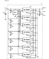
- FIG. 5 is a simplified equivalent circuit diagram of a power supply circuit module to which the circuit board module according to the first embodiment is applied.
- FIG. 6 is an equivalent circuit diagram showing a simplified configuration of a power conversion unit of the power supply circuit module shown in FIG.
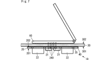
- FIG. 7 is a side sectional view showing a partial configuration of an electronic device to which the circuit board module according to the first embodiment is applied.
- FIG. 1 is an external perspective view of the circuit board module according to the first embodiment.
- FIG. 2 is an exploded perspective view of the circuit board module according to the first embodiment.
- FIG. 3 is a plan view of the circuit board module according to the first embodiment.
- FIG. 4 is
- FIG. 8 is a side sectional view of the circuit board module according to the second embodiment.
- FIG. 9 is a side sectional view of the circuit board module according to the third embodiment.
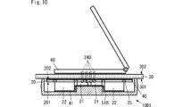
- FIG. 10 is a side sectional view showing a partial configuration of an electronic device to which the circuit board module according to the third embodiment is applied.
- FIG. 11 is an external perspective view of the circuit board module according to the fourth embodiment.
- FIG. 12 is an external perspective view of the circuit board module according to the fifth embodiment.
- FIG. 13 is a plan view of the circuit board module according to the sixth embodiment.
- FIG. 1 is an external perspective view of the circuit board module according to the first embodiment.
- FIG. 2 is an exploded perspective view of the circuit board module according to the first embodiment.
- FIG. 3 is a plan view of the circuit board module according to the first embodiment.
- FIG. 4 is a side sectional view of the circuit board module according to the first embodiment. Note that FIG. 4 schematically shows the AA cross section shown in FIG. Further, in FIGS. 1, 2, 3, and 4, some reference numerals are omitted in order to make the figures easier to see.
- the circuit board module 10 includes a circuit board 20, a circuit board 30, and a heat conduction sheet 40.
- the circuit board 20 is made of an insulating base material.
- the circuit board 20 is a flat plate having a first main surface 201 and a second main surface 202. Although not shown, the circuit board 20 is formed with a conductor pattern for realizing a power conversion circuit described later.
- the circuit board 20 corresponds to the "first circuit board" of the present invention.
- a plurality of switching ICs 21 and a plurality of inductors 22 are mounted on the first main surface 201 of the circuit board 20.
- the plurality of switching ICs 21 are mainly the “electronic devices with heat generation” of the present invention.
- the plurality of inductors 22 may also be included in the “electronic device with heat generation” of the present invention.
- the “electronic device with heat generation” of the present invention may be a power semiconductor.
- the plurality of switching ICs 21 are mounted on the circuit board 20 in a predetermined arrangement.
- the plurality of inductors 22 are mounted on the circuit board 20 in a predetermined arrangement so as to sandwich the mounting regions of the plurality of switching ICs 21.
- the plurality of switching ICs 21 and the plurality of inductors 22 are arranged close to each other for each power conversion unit (see FIGS. 4 and 5).
- the plurality of switching ICs 21 and the plurality of inductors 22 are mounted in a central region of the circuit board 20 in a plan view, for example, as shown in FIGS. 1, 2, and 3.
- the mounting area of the plurality of switching ICs 21 and the plurality of inductors 22 is not limited to this.
- a plurality of external terminal conductors 24 are formed on the circuit board 20.
- the plurality of external terminal conductors 24 have, for example, a conductor pattern such as a substantially circular shape or a rectangular shape, and are formed on the second main surface 202 of the circuit board 20.
- the plurality of external terminal conductors 24 are arranged in a region different from the mounting region of the plurality of switching ICs 21 and the mounting region of the plurality of inductors 22 in the plan view of the circuit board 20.
- the plurality of external terminal conductors 24 are arranged in a predetermined pattern near the side surface of the circuit board 20.
- a plurality of heat conductive vias 25 are formed on the circuit board 20.
- the plurality of heat conductive vias 25 penetrate from the first main surface 201 to the second main surface 202 of the circuit board 20.
- the plurality of heat conductive vias 25 are made of a material having high heat conductivity such as a predetermined metal. Specifically, in the plurality of heat conductive vias 25, a through hole penetrating from the first main surface 201 to the second main surface 202 of the circuit board 20 is filled with a heat conductive member having high thermal conductivity. Is feasible.
- the plurality of heat conductive vias 25 may also serve as via conductors for forming a circuit on the circuit board 20, for example.
- the plurality of heat conductive vias 25 preferably have a larger cross-sectional area than the via conductors for forming the circuit.
- the plurality of heat conductive vias 25 are densely distributed in a region near the mounting terminal (conductor pattern) on which the plurality of switching ICs 21 are mounted.
- the fact that the heat conductive via 25 is in the vicinity of the mounting terminal means that, for example, there is no space between the heat conductive via 25 and the mounting terminal about the size of the heat conductive via 25, or the heat conductive via 25 and the heat conductive via 25. It can be defined by the state in which no other conductor pattern is formed between the mounting terminal and the mounting terminal.
- This definition is an example, and the heat propagating from the plurality of switching ICs 21 to the mounting terminals propagates to the heat conductive via 25 with higher efficiency than propagating to the other through the conductor pattern for the circuit and the via conductor for the circuit. It can be defined that the heat conductive via 25 is formed in the vicinity of the mounting terminal.
- the plurality of heat conductive vias 25 are densely distributed in a region near the mounting terminal (conductor pattern) on which the plurality of inductors 22 are mounted.
- the definition of the neighborhood for the mounting terminals of the plurality of inductors 22 is the same as the definition of the neighborhood for the mounting terminals of the plurality of switching ICs 21, and the description thereof will be omitted.
- the circuit board 30 is made of an insulating base material.
- the circuit board 30 is a flat plate having a third main surface 301 and a fourth main surface 302.
- the circuit board 30 is, for example, a motherboard of an electronic device such as a personal computer.
- the plane area of the circuit board 30 is larger than the plane area of the circuit board 20, and it is preferable that the plane area is significantly larger.
- the circuit board 30 corresponds to the "second circuit board" of the present invention.
- a plurality of land conductors 311 are formed on the third main surface 301 of the circuit board 30.
- the heat conductive sheet 40 is a film having a high thermal conductivity.
- the heat conduction sheet 40 preferably has flexibility.
- the area of the heat conduction sheet 40 is substantially the same as the area of the circuit board 20 (the area of the second main surface 202).
- the heat conduction sheet 40 is realized by, for example, a graphite sheet or a silicone sheet.
- the heat conduction sheet 40 corresponds to the "first heat conduction sheet" of the present invention. When a graphite sheet is used, it is better to use a graphite sheet having a higher thermal conductivity than that of metal. As a result, the heat dissipation efficiency described later is further improved.
- the circuit board 20 is arranged with respect to the circuit board 30 so that the second main surface 202 faces the third main surface 301 of the circuit board 30.
- the plurality of land conductors 311 of the circuit board 30 are joined to the plurality of external terminal conductors 24 of the circuit board 20 via a conductive bonding material such as solder.
- solder a conductive bonding material
- the heat conduction sheet 40 is arranged between the circuit board 20 and the circuit board 30, and comes into surface contact with the circuit board 20 and the circuit board 30.
- the heat conduction sheet 40 covers the second main surface 202 of the circuit board 20 and the portion of the third main surface 301 of the circuit board 30 that faces the second main surface 202.
- the heat conduction sheet 40 physically contacts the plurality of heat conduction vias 25 of the circuit board 20.
- the circuit board module 10 can conduct heat generated from the plurality of switching ICs 21 to the circuit board 30 through the base material of the circuit board 20, the conductor pattern for the circuit, and the heat conduction sheet 40. .. Further, the circuit board module 10 can conduct heat generated from the plurality of switching ICs 21 to the circuit board 30 through the plurality of heat conductive vias 25 and the heat conductive sheet 40. Since the circuit board 30 has a larger area than the circuit board 20, the propagated heat is effectively dissipated.
- the circuit board module 10 can more effectively conduct heat generated from the plurality of switching ICs 21 to the heat conduction sheet 40 by providing the plurality of heat conduction vias 25.
- the heat conduction sheet 40 is larger than the total area of the plurality of heat conduction vias 25, is larger than the area where the plurality of switching ICs 21 are mounted, and is larger than the area where the plurality of inductors 22 are mounted.
- the generated heat can be further diffused in a planar shape and conducted to the circuit board 30.
- the circuit board 30 having a larger area than the heat conduction sheet 40 further diffuses the heat, and more efficient heat dissipation can be realized.
- the circuit board module 10 can more effectively dissipate heat from electronic components that generate heat. Further, since the circuit board module 10 does not use the heat radiation fins as shown in the conventional configuration, it is possible to realize a low profile. That is, the circuit board module 10 can realize excellent heat dissipation and low profile.
- the heat conduction sheet 40 when the heat conduction sheet 40 has flexibility, it is preferable to sandwich the heat conduction sheet 40 between the circuit board 20 and the circuit board 30 so as to apply a predetermined pressure. Having flexibility means that it is easily deformed by an external force or the like. As a result, the adhesion between the heat conduction sheet 40 and the circuit board 20 and the circuit board 30 is improved. Further, the adhesion between the heat conductive sheet 40 and the plurality of heat conductive vias 25 is improved. As a result, the circuit board module 10 can realize even higher heat dissipation.
- a silicone sheet may be used if there is a purpose of preventing an unnecessary short circuit between the circuit board 20 and the circuit board 30.
- the heat conduction sheet 40 when it is not necessary for the heat conduction sheet 40 to prevent such a short circuit, or as shown in the second embodiment described later, the heat conduction sheet 40 must be positively conducted.
- a graphite sheet may be used. When a graphite sheet is used, it can be combined with the circuit board 20 by providing an insulating resist film at necessary positions on the second main surface 202 of the circuit board 20 and the third main surface 301 of the circuit board 30 facing each other. Unnecessary short circuit with the circuit board 30 can be prevented.
- the heat conduction sheet 40 is not arranged in the forming region of the plurality of external terminal conductors 24 on the circuit board 20.
- the heat conductive sheet 40 is a conductive sheet (for example, a graphite sheet)
- unnecessary short circuits can be suppressed
- the heat conductive sheet 40 is an insulating sheet (for example, a silicone sheet)
- unnecessary short circuits can be suppressed. Unnecessary disconnection can be suppressed.
- FIG. 5 is a simplified equivalent circuit diagram of a power supply circuit module to which the circuit board module according to the first embodiment is applied.
- FIG. 6 is an equivalent circuit diagram showing a simplified configuration of a power conversion unit of the power supply circuit module shown in FIG. The specific configuration and operation of the power supply circuit module will not be described.
- the power supply circuit module 2 includes an MPU 901, a plurality of power conversion units 911-917, a voltage detection circuit 902, and a plurality of input capacitors Ci1-Ci7.
- the plurality of power conversion units 911-917 are connected to the input terminal Pin and are supplied with the input voltage Vi from the outside.
- Input capacitors Ci1-Ci7 are connected to the input ends of the plurality of power conversion units 911-917, respectively.
- a plurality of power conversion units 911-917 are connected to a pair of terminals including an output terminal Pout + and an output terminal Pout ⁇ .
- An output capacitor Co is connected between the output terminal Pout + and the output terminal Pout ⁇ .
- the MPU 901 is connected to the input terminal Pin and is supplied with the input voltage Vi.
- the MPU 901 is connected to a plurality of power conversion units 911-917.
- the voltage detection circuit 902 is connected to the output terminal Pout +, and the detected voltage is given to a plurality of power conversion units 911-917.
- the MPU 901 is driven by a drive voltage obtained from the input voltage Vi, and controls on / off of a plurality of power conversion units 911-917 based on the voltage detected by the voltage detection circuit 902. That is, the MPU 901 controls the number of power converters to be operated by the plurality of power conversion units 911-917 according to the state of the load connected to the output terminal Pout. Specifically, for example, in the MPU 901, if the current supplied to the load is increased, the number of power conversion units to be operated is increased, and if the current supplied to the load is excessive, the number of power conversion units to be operated is increased. To reduce.
- the power supply circuit module 2 can supply current according to the load state. Further, in this configuration, a plurality of power conversion units 911-917 are connected in parallel to the load, so that the power supply circuit module 2 supplies a large current to the load while having a low voltage. can do.
- the plurality of power conversion units 911-917 have the same configuration, and roughly include the configuration shown in FIG. In the following, the power conversion unit 911 will be described as an example with reference to FIG.
- the power conversion unit 911 includes a switching IC 21, an inductor 22, a feedback signal generation circuit 921, and an output capacitor Co.
- the switching IC 21 includes a plurality of switching elements and a control unit for the switching elements inside.
- the switching IC 21 operates by receiving a clock signal from the MPU 901.
- the switching IC 21 is connected to the inductor 22, and the inductor 22 is connected to the output terminal Pout.
- An output capacitor Co is connected to the output terminal Pout side of the inductor 22.
- the feedback signal generation circuit 921 generates a feedback signal by using the Sense signal corresponding to the output current and the output voltage and the inductor current, and gives the feedback signal to the switching IC 21.
- the switching IC 21 controls the output current and output voltage based on the feedback signal.
- the switching IC 21 switches on / off of a plurality of switching elements at high speed. As a result, the switching IC 21 generates heat. That is, the switching IC 21 corresponds to the electronic device with heat generation of the present application. Therefore, the configuration of the circuit board module 10 of the present application works more effectively.
- the switching IC 21 and the inductor 22 correspond to the electronic device with heat generation of the present application. Therefore, the configuration of the circuit board module 10 of the present application works more effectively.
- FIG. 7 is a side sectional view showing a partial configuration of an electronic device to which the circuit board module according to the first embodiment is applied.
- the electronic device includes the configuration of the circuit board module 10 and the socket 60.
- the socket 60 is mounted on the fourth main surface 302 of the circuit board 30.
- the socket 60 overlaps the circuit board 20 in a plan view.
- the socket 60 may be equipped with a function as a radiator.
- a semiconductor device for data processing such as a CPU and MPU is mounted on the socket 60.
- the semiconductor device mounted in the socket 60 is driven by receiving power supply from a power supply circuit module (for example, the power supply circuit module 2 shown in FIGS. 5 and 6 described above) realized by the circuit board 20.
- a power supply circuit module for example, the power supply circuit module 2 shown in FIGS. 5 and 6 described above
- the configuration of the circuit board module 10 enables effective heat dissipation. Therefore, the adverse effect on the semiconductor device is suppressed, and the reliability of the electronic device is improved. Further, in this configuration, since the circuit board module 10 is short, even if the power supply circuit module is arranged on the back surface of the semiconductor device, it is possible to suppress the heightening of the electronic device.
- a radiator may be attached to the socket 60, for example.
- the circuit board 20 is similarly provided with a radiator, the electronic device becomes even taller.
- the circuit board module 10 since the circuit board 20 does not require a tall radiator, it is possible to suppress the heightening of the electronic device.
- the circuit board 20 that realizes the power supply circuit module is arranged so as to overlap the semiconductor device, the distance between the power supply circuit module and the semiconductor device is shortened. Therefore, the power supply efficiency from the power supply circuit module to the semiconductor device is high, and the accuracy and stability of the supply voltage to the semiconductor device are also improved.
- FIG. 8 is a side sectional view of the circuit board module according to the second embodiment.
- the circuit board module 10A according to the second embodiment has a ground conductor 26 and an insulating resist film on the circuit board 20 with respect to the circuit board module 10 according to the first embodiment. It differs in the point that 27 is provided and the part related thereto.
- the other configurations of the circuit board module 10A are the same as those of the circuit board module 10, and the description of the same parts will be omitted.
- the circuit board module 10A includes a flat-film ground conductor 26 and an insulating resist film 27.
- the ground conductor 26 is formed on the second main surface 202 of the circuit board 20.
- the ground conductor 26 is connected to a plurality of heat conductive vias 25.
- the resist film 27 is formed so as to cover the ground conductor 26.
- An opening 270 is formed in the resist film 27.
- the ground conductor 26 is partially exposed to the circuit board 30 side by the opening 270.
- the heat conductive sheet 40 is made of a conductive material such as a graphite sheet.
- the heat conduction sheet 40 is in contact with and in close contact with the ground conductor 26 by being pressed as described above. That is, the heat conduction sheet 40 and the ground conductor 26 are in physical and electrical contact with each other through the opening 270.
- the heat of the plurality of switching ICs 21 and the plurality of inductors 22 is dissipated through the plurality of heat conductive vias 25, the ground conductor 26, and the heat conductive sheet 40.
- the heat conduction sheet 40 functions as a noise shielding film.
- the circuit board module 10A can suppress the noise generated from the electronic components mounted on the circuit board 20, such as the noise generated from the plurality of switching ICs 21, from propagating to the circuit board 30 side.
- the circuit board module 10A can suppress the noise generated from the electronic components mounted on the circuit board 20 from propagating to the semiconductor device.
- the heat conduction sheet 40 has a shape that extends over substantially the entire surface of the circuit board 20, so that the circuit board module 10A can shield noise over a wide range.
- FIG. 9 is a side sectional view of the circuit board module according to the third embodiment.
- the circuit board module 10B according to the third embodiment further includes a heat conduction sheet 41 and a heat sink 51 with respect to the circuit board module 10 according to the first embodiment. Is different. Other configurations of the circuit board module 10B are the same as those of the circuit board module 10, and the description of the same parts will be omitted.
- the circuit board module 10B includes a heat conduction sheet 41 and a heat sink 51.
- the heat conduction sheet 41 is an insulating sheet such as silicone rubber.
- the heat conduction sheet 41 comes into contact with the surfaces of the plurality of switching ICs 21 and the plurality of inductors 22 opposite to the mounting surface side.
- the heat radiating plate 51 comes into contact with the surface of the heat conduction sheet 41 opposite to the contact surface with the plurality of switching ICs 21 and the plurality of inductors 22.
- the heat conduction sheet 41 corresponds to the "second heat conduction sheet" of the present invention.
- the circuit board module 10B can dissipate heat through the heat radiating plate 51 in addition to the heat radiating from the heat conduction sheet 40 to the circuit board 30.
- the area of the heat sink 51 is preferably larger than the total area of the plurality of switching ICs 21 and the total area of the plurality of inductors 22. As a result, the heat dissipation efficiency is further improved.
- the circuit board module 10B having such a configuration can be applied to, for example, an electronic device as shown in FIG.
- FIG. 10 is a side sectional view showing a partial configuration of an electronic device to which the circuit board module according to the third embodiment is applied.
- the electronic device shown in FIG. 10 is different from the electronic device of the first embodiment shown in FIG. 7 in that it is provided with a back plate 51B for a socket and the heat conduction sheet 41 described above.
- Other configurations of the electronic device shown in FIG. 10 are the same as those of the electronic device shown in FIG. 7, and the description of the same parts will be omitted.
- the back plate 51B is fixed to the third main surface 301 of the circuit board 30.
- the back plate 51B is arranged so as to surround the circuit board 20.
- the back plate 51B contacts the plurality of switching ICs 21 and the plurality of inductors 22 via the heat conduction sheet 41.
- the back plate 51B is made of a material having the same thermal conductivity as the heat sink 51 described above.
- the electronic device shown in FIG. 10 can dissipate heat using the back plate 51B as well. Further, since the back plate 51B is fixed to the circuit board 30, heat can be conducted from the back plate 51B to the circuit board 30, which enables more effective heat dissipation.
- FIG. 11 is an external perspective view of the circuit board module according to the fourth embodiment.
- the circuit board module 10C according to the fourth embodiment is different from the circuit board module 10 according to the first embodiment in the shape of the heat conduction sheet 40C.
- Other configurations of the circuit board module 10C are the same as those of the circuit board module 10, and the description of the same parts will be omitted.
- the circuit board module 10C includes a heat conduction sheet 40C.
- the area of the heat conduction sheet 40C is smaller than the area of the circuit board 20. At this time, the area of the heat conduction sheet 40C is larger than the total area of the area of the mounting area of the plurality of switching ICs 21 and the area of the mounting area of the plurality of inductors 22. Further, the heat conductive sheet 40C overlaps all of the plurality of heat conductive vias 25 in a plan view.
- the circuit board module 10C can realize excellent heat dissipation and low profile.
- FIG. 12 is an external perspective view of the circuit board module according to the fifth embodiment.
- the circuit board module 10D according to the fifth embodiment is different from the circuit board module 10 according to the first embodiment in the shape of the heat conduction sheet 40D.
- Other configurations of the circuit board module 10D are the same as those of the circuit board module 10, and the description of the same parts will be omitted.
- the circuit board module 10D includes a heat conduction sheet 40D.
- the area of the heat conduction sheet 40D is larger than the area of the circuit board 20.
- the circuit board module 10D can realize further excellent heat dissipation as compared with the circuit board module 10, and can realize a low profile.
- FIG. 13 is a plan view of the circuit board module according to the sixth embodiment.
- the circuit board module 10E according to the sixth embodiment is different from the circuit board module 10 according to the first embodiment in the arrangement number and arrangement pattern of the plurality of heat conductive vias 25.
- Other configurations of the circuit board module 10E are the same as those of the circuit board module 10, and the description of the same parts will be omitted.
- a plurality of heat conductive vias 25 are formed more around the plurality of switching ICs 21.
- the circuit board module 10E can further improve the heat dissipation efficiency of the plurality of switching ICs 21 which are the main heat generating sources.
- the mode of improving the partial heat dissipation efficiency by the number of the plurality of heat conductive vias 25 is shown, but the partial heat dissipation is shown by changing the cross-sectional area of the plurality of heat conductive vias 25. It is also possible to improve efficiency. Furthermore, it is also possible to improve the partial heat dissipation efficiency by combining the number and the cross-sectional area.
Landscapes
- Engineering & Computer Science (AREA)
- Theoretical Computer Science (AREA)
- Microelectronics & Electronic Packaging (AREA)
- Physics & Mathematics (AREA)
- General Engineering & Computer Science (AREA)
- Computer Hardware Design (AREA)
- General Physics & Mathematics (AREA)
- Human Computer Interaction (AREA)
- Thermal Sciences (AREA)
- Structure Of Printed Boards (AREA)
- Cooling Or The Like Of Semiconductors Or Solid State Devices (AREA)
- Cooling Or The Like Of Electrical Apparatus (AREA)
Priority Applications (2)
| Application Number | Priority Date | Filing Date | Title |
|---|---|---|---|
| JP2022508050A JP7494901B2 (ja) | 2020-03-18 | 2020-11-24 | 回路基板モジュール |
| US17/933,116 US12446144B2 (en) | 2020-03-18 | 2022-09-18 | Circuit board module |
Applications Claiming Priority (2)
| Application Number | Priority Date | Filing Date | Title |
|---|---|---|---|
| JP2020-047121 | 2020-03-18 | ||
| JP2020047121 | 2020-03-18 |
Related Child Applications (1)
| Application Number | Title | Priority Date | Filing Date |
|---|---|---|---|
| US17/933,116 Continuation US12446144B2 (en) | 2020-03-18 | 2022-09-18 | Circuit board module |
Publications (1)
| Publication Number | Publication Date |
|---|---|
| WO2021186797A1 true WO2021186797A1 (ja) | 2021-09-23 |
Family
ID=77771192
Family Applications (1)
| Application Number | Title | Priority Date | Filing Date |
|---|---|---|---|
| PCT/JP2020/043644 Ceased WO2021186797A1 (ja) | 2020-03-18 | 2020-11-24 | 回路基板モジュール |
Country Status (3)
| Country | Link |
|---|---|
| US (1) | US12446144B2 (https=) |
| JP (1) | JP7494901B2 (https=) |
| WO (1) | WO2021186797A1 (https=) |
Citations (3)
| Publication number | Priority date | Publication date | Assignee | Title |
|---|---|---|---|---|
| JPS6183098U (https=) * | 1984-11-06 | 1986-06-02 | ||
| JP2006093526A (ja) * | 2004-09-27 | 2006-04-06 | Matsushita Electric Ind Co Ltd | 導電性熱伝導シート |
| JP2014029977A (ja) * | 2012-07-05 | 2014-02-13 | Fujikura Ltd | 電子装置の放熱構造 |
Family Cites Families (14)
| Publication number | Priority date | Publication date | Assignee | Title |
|---|---|---|---|---|
| US5739581A (en) * | 1995-11-17 | 1998-04-14 | National Semiconductor Corporation | High density integrated circuit package assembly with a heatsink between stacked dies |
| US6118177A (en) * | 1998-11-17 | 2000-09-12 | Lucent Technologies, Inc. | Heatspreader for a flip chip device, and method for connecting the heatspreader |
| JP2004140286A (ja) * | 2002-10-21 | 2004-05-13 | Nec Semiconductors Kyushu Ltd | 半導体装置及びその製造方法 |
| TWI273379B (en) * | 2004-09-30 | 2007-02-11 | Asustek Comp Inc | Heat sink module |
| US7623349B2 (en) * | 2005-03-07 | 2009-11-24 | Ati Technologies Ulc | Thermal management apparatus and method for a circuit substrate |
| DE102005063281A1 (de) * | 2005-12-30 | 2007-07-05 | Robert Bosch Gmbh | Integriertes elektronisches Bauteil sowie Kühlvorrichtung für ein integriertes elektronisches Bauteil |
| US7808013B2 (en) * | 2006-10-31 | 2010-10-05 | Cree, Inc. | Integrated heat spreaders for light emitting devices (LEDs) and related assemblies |
| JP5388598B2 (ja) | 2008-11-14 | 2014-01-15 | カルソニックカンセイ株式会社 | 素子の放熱構造 |
| TW201103381A (en) * | 2009-07-03 | 2011-01-16 | qi-rui Cai | High heat dissipation circuit board and fabrication method thereof |
| US9209141B2 (en) * | 2014-02-26 | 2015-12-08 | International Business Machines Corporation | Shielded package assemblies with integrated capacitor |
| JP6112073B2 (ja) * | 2014-06-20 | 2017-04-12 | 株式会社豊田自動織機 | 半導体装置 |
| US10199904B2 (en) * | 2017-02-23 | 2019-02-05 | Schaft Inc. | Cooling a heat-generating electronic device |
| CN111801794B (zh) * | 2018-03-14 | 2024-10-18 | 三菱电机株式会社 | 半导体功率模块以及电力变换装置 |
| CN210325761U (zh) * | 2018-12-29 | 2020-04-14 | 华为技术有限公司 | 一种芯片装置及电子设备 |
-
2020
- 2020-11-24 JP JP2022508050A patent/JP7494901B2/ja active Active
- 2020-11-24 WO PCT/JP2020/043644 patent/WO2021186797A1/ja not_active Ceased
-
2022
- 2022-09-18 US US17/933,116 patent/US12446144B2/en active Active
Patent Citations (3)
| Publication number | Priority date | Publication date | Assignee | Title |
|---|---|---|---|---|
| JPS6183098U (https=) * | 1984-11-06 | 1986-06-02 | ||
| JP2006093526A (ja) * | 2004-09-27 | 2006-04-06 | Matsushita Electric Ind Co Ltd | 導電性熱伝導シート |
| JP2014029977A (ja) * | 2012-07-05 | 2014-02-13 | Fujikura Ltd | 電子装置の放熱構造 |
Also Published As
| Publication number | Publication date |
|---|---|
| US12446144B2 (en) | 2025-10-14 |
| US20230009649A1 (en) | 2023-01-12 |
| JPWO2021186797A1 (https=) | 2021-09-23 |
| JP7494901B2 (ja) | 2024-06-04 |
Similar Documents
| Publication | Publication Date | Title |
|---|---|---|
| JP7136553B2 (ja) | 電子制御装置 | |
| JPH1174427A (ja) | 回路素子の放熱構造 | |
| EP3327767B1 (en) | Mount structure, method of manufacturing mount structure, and wireless device | |
| JP2004071670A (ja) | Icパッケージ、接続構造、および電子機器 | |
| WO2009110045A1 (ja) | 発熱体搭載部品の取付構造 | |
| JP2010129877A (ja) | 電子部品モジュール | |
| CN114078792A (zh) | 半导体封装件、半导体装置、半导体封装件搭载设备、以及半导体装置搭载设备 | |
| KR20050002659A (ko) | 혼성집적회로 | |
| WO2017022221A1 (ja) | 放熱構造および電子機器 | |
| US12193143B2 (en) | Circuit board module | |
| JP4828969B2 (ja) | 半導体装置の実装構造 | |
| JP7494901B2 (ja) | 回路基板モジュール | |
| US6061260A (en) | Board mounted power supply having an auxiliary output | |
| JP5024314B2 (ja) | 半導体素子の放熱構造およびこれを備えた電子機器 | |
| JP2020191316A (ja) | 回路モジュール | |
| KR20160008345A (ko) | 전자부품 패키지 | |
| JPH1098287A (ja) | 回路基板モジュールの冷却装置およびこの冷却装置を有する携帯形電子機器 | |
| JP2001068879A (ja) | 制御機器 | |
| CN222147879U (zh) | 电路板组件 | |
| JPH09102685A (ja) | 電子装置の放熱構造 | |
| TWI898918B (zh) | 電子組件 | |
| JP7307844B2 (ja) | 電子制御装置 | |
| JPWO2004112450A1 (ja) | 基板実装方法及び実装構造 | |
| JP6676212B2 (ja) | 電子モジュール及び電源装置 | |
| JP7060426B2 (ja) | 基板の伝熱構造 |
Legal Events
| Date | Code | Title | Description |
|---|---|---|---|
| 121 | Ep: the epo has been informed by wipo that ep was designated in this application |
Ref document number: 20925102 Country of ref document: EP Kind code of ref document: A1 |
|
| ENP | Entry into the national phase |
Ref document number: 2022508050 Country of ref document: JP Kind code of ref document: A |
|
| NENP | Non-entry into the national phase |
Ref country code: DE |
|
| 122 | Ep: pct application non-entry in european phase |
Ref document number: 20925102 Country of ref document: EP Kind code of ref document: A1 |