WO2021186538A1 - ラミネートブスバー、電力変換器、電力変換装置および無停電電源装置 - Google Patents
ラミネートブスバー、電力変換器、電力変換装置および無停電電源装置 Download PDFInfo
- Publication number
- WO2021186538A1 WO2021186538A1 PCT/JP2020/011682 JP2020011682W WO2021186538A1 WO 2021186538 A1 WO2021186538 A1 WO 2021186538A1 JP 2020011682 W JP2020011682 W JP 2020011682W WO 2021186538 A1 WO2021186538 A1 WO 2021186538A1
- Authority
- WO
- WIPO (PCT)
- Prior art keywords
- terminal
- fuse
- length direction
- power converter
- bus bar
- Prior art date
- Legal status (The legal status is an assumption and is not a legal conclusion. Google has not performed a legal analysis and makes no representation as to the accuracy of the status listed.)
- Ceased
Links
Images




Classifications
-
- H—ELECTRICITY
- H02—GENERATION; CONVERSION OR DISTRIBUTION OF ELECTRIC POWER
- H02G—INSTALLATION OF ELECTRIC CABLES OR LINES, OR OF COMBINED OPTICAL AND ELECTRIC CABLES OR LINES
- H02G5/00—Installations of bus-bars
- H02G5/005—Laminated bus-bars
-
- H—ELECTRICITY
- H02—GENERATION; CONVERSION OR DISTRIBUTION OF ELECTRIC POWER
- H02J—ELECTRIC POWER NETWORKS; CIRCUIT ARRANGEMENTS OR SYSTEMS FOR SUPPLYING OR DISTRIBUTING ELECTRIC POWER; SYSTEMS FOR STORING ELECTRIC ENERGY
- H02J9/00—Circuit arrangements for emergency or stand-by power supply, e.g. for emergency lighting
- H02J9/04—Circuit arrangements for emergency or stand-by power supply, e.g. for emergency lighting in which the distribution system is disconnected from the normal source and connected to a standby source
- H02J9/06—Circuit arrangements for emergency or stand-by power supply, e.g. for emergency lighting in which the distribution system is disconnected from the normal source and connected to a standby source with automatic change-over, e.g. UPS systems
- H02J9/062—Circuit arrangements for emergency or stand-by power supply, e.g. for emergency lighting in which the distribution system is disconnected from the normal source and connected to a standby source with automatic change-over, e.g. UPS systems for AC powered loads
-
- H—ELECTRICITY
- H01—ELECTRIC ELEMENTS
- H01R—ELECTRICALLY-CONDUCTIVE CONNECTIONS; STRUCTURAL ASSOCIATIONS OF A PLURALITY OF MUTUALLY-INSULATED ELECTRICAL CONNECTING ELEMENTS; COUPLING DEVICES; CURRENT COLLECTORS
- H01R25/00—Coupling parts adapted for simultaneous co-operation with two or more identical counterparts, e.g. for distributing energy to two or more circuits
- H01R25/16—Rails or bus-bars provided with a plurality of discrete connecting locations for counterparts
-
- H—ELECTRICITY
- H02—GENERATION; CONVERSION OR DISTRIBUTION OF ELECTRIC POWER
- H02J—ELECTRIC POWER NETWORKS; CIRCUIT ARRANGEMENTS OR SYSTEMS FOR SUPPLYING OR DISTRIBUTING ELECTRIC POWER; SYSTEMS FOR STORING ELECTRIC ENERGY
- H02J9/00—Circuit arrangements for emergency or stand-by power supply, e.g. for emergency lighting
- H02J9/04—Circuit arrangements for emergency or stand-by power supply, e.g. for emergency lighting in which the distribution system is disconnected from the normal source and connected to a standby source
- H02J9/06—Circuit arrangements for emergency or stand-by power supply, e.g. for emergency lighting in which the distribution system is disconnected from the normal source and connected to a standby source with automatic change-over, e.g. UPS systems
-
- H—ELECTRICITY
- H02—GENERATION; CONVERSION OR DISTRIBUTION OF ELECTRIC POWER
- H02M—APPARATUS FOR CONVERSION BETWEEN AC AND AC, BETWEEN AC AND DC, OR BETWEEN DC AND DC, AND FOR USE WITH MAINS OR SIMILAR POWER SUPPLY SYSTEMS; CONVERSION OF DC OR AC INPUT POWER INTO SURGE OUTPUT POWER; CONTROL OR REGULATION THEREOF
- H02M5/00—Conversion of AC power input into AC power output, e.g. for change of voltage, for change of frequency, for change of number of phases
- H02M5/40—Conversion of AC power input into AC power output, e.g. for change of voltage, for change of frequency, for change of number of phases with intermediate conversion into DC
- H02M5/42—Conversion of AC power input into AC power output, e.g. for change of voltage, for change of frequency, for change of number of phases with intermediate conversion into DC by static converters
- H02M5/44—Conversion of AC power input into AC power output, e.g. for change of voltage, for change of frequency, for change of number of phases with intermediate conversion into DC by static converters using discharge tubes or semiconductor devices to convert the intermediate DC into AC
- H02M5/453—Conversion of AC power input into AC power output, e.g. for change of voltage, for change of frequency, for change of number of phases with intermediate conversion into DC by static converters using discharge tubes or semiconductor devices to convert the intermediate DC into AC using devices of a triode or transistor type requiring continuous application of a control signal
- H02M5/458—Conversion of AC power input into AC power output, e.g. for change of voltage, for change of frequency, for change of number of phases with intermediate conversion into DC by static converters using discharge tubes or semiconductor devices to convert the intermediate DC into AC using devices of a triode or transistor type requiring continuous application of a control signal using semiconductor devices only
- H02M5/4585—Conversion of AC power input into AC power output, e.g. for change of voltage, for change of frequency, for change of number of phases with intermediate conversion into DC by static converters using discharge tubes or semiconductor devices to convert the intermediate DC into AC using devices of a triode or transistor type requiring continuous application of a control signal using semiconductor devices only having a rectifier with controlled elements
-
- H—ELECTRICITY
- H02—GENERATION; CONVERSION OR DISTRIBUTION OF ELECTRIC POWER
- H02M—APPARATUS FOR CONVERSION BETWEEN AC AND AC, BETWEEN AC AND DC, OR BETWEEN DC AND DC, AND FOR USE WITH MAINS OR SIMILAR POWER SUPPLY SYSTEMS; CONVERSION OF DC OR AC INPUT POWER INTO SURGE OUTPUT POWER; CONTROL OR REGULATION THEREOF
- H02M7/00—Conversion of AC power input into DC power output; Conversion of DC power input into AC power output
- H02M7/003—Constructional details, e.g. physical layout, assembly, wiring or busbar connections
-
- H—ELECTRICITY
- H02—GENERATION; CONVERSION OR DISTRIBUTION OF ELECTRIC POWER
- H02M—APPARATUS FOR CONVERSION BETWEEN AC AND AC, BETWEEN AC AND DC, OR BETWEEN DC AND DC, AND FOR USE WITH MAINS OR SIMILAR POWER SUPPLY SYSTEMS; CONVERSION OF DC OR AC INPUT POWER INTO SURGE OUTPUT POWER; CONTROL OR REGULATION THEREOF
- H02M7/00—Conversion of AC power input into DC power output; Conversion of DC power input into AC power output
- H02M7/02—Conversion of AC power input into DC power output without possibility of reversal
- H02M7/04—Conversion of AC power input into DC power output without possibility of reversal by static converters
- H02M7/06—Conversion of AC power input into DC power output without possibility of reversal by static converters using discharge tubes without control electrode or semiconductor devices without control electrode
- H02M7/08—Conversion of AC power input into DC power output without possibility of reversal by static converters using discharge tubes without control electrode or semiconductor devices without control electrode arranged for operation in parallel
-
- H—ELECTRICITY
- H02—GENERATION; CONVERSION OR DISTRIBUTION OF ELECTRIC POWER
- H02M—APPARATUS FOR CONVERSION BETWEEN AC AND AC, BETWEEN AC AND DC, OR BETWEEN DC AND DC, AND FOR USE WITH MAINS OR SIMILAR POWER SUPPLY SYSTEMS; CONVERSION OF DC OR AC INPUT POWER INTO SURGE OUTPUT POWER; CONTROL OR REGULATION THEREOF
- H02M7/00—Conversion of AC power input into DC power output; Conversion of DC power input into AC power output
- H02M7/02—Conversion of AC power input into DC power output without possibility of reversal
- H02M7/04—Conversion of AC power input into DC power output without possibility of reversal by static converters
- H02M7/12—Conversion of AC power input into DC power output without possibility of reversal by static converters using discharge tubes with control electrode or semiconductor devices with control electrode
- H02M7/21—Conversion of AC power input into DC power output without possibility of reversal by static converters using discharge tubes with control electrode or semiconductor devices with control electrode using devices of a triode or transistor type requiring continuous application of a control signal
- H02M7/217—Conversion of AC power input into DC power output without possibility of reversal by static converters using discharge tubes with control electrode or semiconductor devices with control electrode using devices of a triode or transistor type requiring continuous application of a control signal using semiconductor devices only
-
- H—ELECTRICITY
- H02—GENERATION; CONVERSION OR DISTRIBUTION OF ELECTRIC POWER
- H02M—APPARATUS FOR CONVERSION BETWEEN AC AND AC, BETWEEN AC AND DC, OR BETWEEN DC AND DC, AND FOR USE WITH MAINS OR SIMILAR POWER SUPPLY SYSTEMS; CONVERSION OF DC OR AC INPUT POWER INTO SURGE OUTPUT POWER; CONTROL OR REGULATION THEREOF
- H02M7/00—Conversion of AC power input into DC power output; Conversion of DC power input into AC power output
- H02M7/42—Conversion of DC power input into AC power output without possibility of reversal
- H02M7/44—Conversion of DC power input into AC power output without possibility of reversal by static converters
- H02M7/48—Conversion of DC power input into AC power output without possibility of reversal by static converters using discharge tubes with control electrode or semiconductor devices with control electrode
- H02M7/493—Conversion of DC power input into AC power output without possibility of reversal by static converters using discharge tubes with control electrode or semiconductor devices with control electrode the static converters being arranged for operation in parallel
-
- H—ELECTRICITY
- H02—GENERATION; CONVERSION OR DISTRIBUTION OF ELECTRIC POWER
- H02M—APPARATUS FOR CONVERSION BETWEEN AC AND AC, BETWEEN AC AND DC, OR BETWEEN DC AND DC, AND FOR USE WITH MAINS OR SIMILAR POWER SUPPLY SYSTEMS; CONVERSION OF DC OR AC INPUT POWER INTO SURGE OUTPUT POWER; CONTROL OR REGULATION THEREOF
- H02M7/00—Conversion of AC power input into DC power output; Conversion of DC power input into AC power output
- H02M7/42—Conversion of DC power input into AC power output without possibility of reversal
- H02M7/44—Conversion of DC power input into AC power output without possibility of reversal by static converters
- H02M7/48—Conversion of DC power input into AC power output without possibility of reversal by static converters using discharge tubes with control electrode or semiconductor devices with control electrode
- H02M7/53—Conversion of DC power input into AC power output without possibility of reversal by static converters using discharge tubes with control electrode or semiconductor devices with control electrode using devices of a triode or transistor type requiring continuous application of a control signal
- H02M7/537—Conversion of DC power input into AC power output without possibility of reversal by static converters using discharge tubes with control electrode or semiconductor devices with control electrode using devices of a triode or transistor type requiring continuous application of a control signal using semiconductor devices only, e.g. single switched pulse inverters
-
- H—ELECTRICITY
- H02—GENERATION; CONVERSION OR DISTRIBUTION OF ELECTRIC POWER
- H02M—APPARATUS FOR CONVERSION BETWEEN AC AND AC, BETWEEN AC AND DC, OR BETWEEN DC AND DC, AND FOR USE WITH MAINS OR SIMILAR POWER SUPPLY SYSTEMS; CONVERSION OF DC OR AC INPUT POWER INTO SURGE OUTPUT POWER; CONTROL OR REGULATION THEREOF
- H02M3/00—Conversion of DC power input into DC power output
- H02M3/22—Conversion of DC power input into DC power output with intermediate conversion into AC
- H02M3/24—Conversion of DC power input into DC power output with intermediate conversion into AC by static converters
- H02M3/28—Conversion of DC power input into DC power output with intermediate conversion into AC by static converters using discharge tubes with control electrode or semiconductor devices with control electrode to produce the intermediate AC
- H02M3/325—Conversion of DC power input into DC power output with intermediate conversion into AC by static converters using discharge tubes with control electrode or semiconductor devices with control electrode to produce the intermediate AC using devices of a triode or a transistor type requiring continuous application of a control signal
- H02M3/335—Conversion of DC power input into DC power output with intermediate conversion into AC by static converters using discharge tubes with control electrode or semiconductor devices with control electrode to produce the intermediate AC using devices of a triode or a transistor type requiring continuous application of a control signal using semiconductor devices only
- H02M3/33569—Conversion of DC power input into DC power output with intermediate conversion into AC by static converters using discharge tubes with control electrode or semiconductor devices with control electrode to produce the intermediate AC using devices of a triode or a transistor type requiring continuous application of a control signal using semiconductor devices only having several active switching elements
- H02M3/33576—Conversion of DC power input into DC power output with intermediate conversion into AC by static converters using discharge tubes with control electrode or semiconductor devices with control electrode to produce the intermediate AC using devices of a triode or a transistor type requiring continuous application of a control signal using semiconductor devices only having several active switching elements having at least one active switching element at the secondary side of an isolation transformer
- H02M3/33584—Bidirectional converters
-
- H—ELECTRICITY
- H02—GENERATION; CONVERSION OR DISTRIBUTION OF ELECTRIC POWER
- H02M—APPARATUS FOR CONVERSION BETWEEN AC AND AC, BETWEEN AC AND DC, OR BETWEEN DC AND DC, AND FOR USE WITH MAINS OR SIMILAR POWER SUPPLY SYSTEMS; CONVERSION OF DC OR AC INPUT POWER INTO SURGE OUTPUT POWER; CONTROL OR REGULATION THEREOF
- H02M5/00—Conversion of AC power input into AC power output, e.g. for change of voltage, for change of frequency, for change of number of phases
- H02M5/40—Conversion of AC power input into AC power output, e.g. for change of voltage, for change of frequency, for change of number of phases with intermediate conversion into DC
- H02M5/42—Conversion of AC power input into AC power output, e.g. for change of voltage, for change of frequency, for change of number of phases with intermediate conversion into DC by static converters
-
- H—ELECTRICITY
- H02—GENERATION; CONVERSION OR DISTRIBUTION OF ELECTRIC POWER
- H02M—APPARATUS FOR CONVERSION BETWEEN AC AND AC, BETWEEN AC AND DC, OR BETWEEN DC AND DC, AND FOR USE WITH MAINS OR SIMILAR POWER SUPPLY SYSTEMS; CONVERSION OF DC OR AC INPUT POWER INTO SURGE OUTPUT POWER; CONTROL OR REGULATION THEREOF
- H02M7/00—Conversion of AC power input into DC power output; Conversion of DC power input into AC power output
- H02M7/42—Conversion of DC power input into AC power output without possibility of reversal
- H02M7/44—Conversion of DC power input into AC power output without possibility of reversal by static converters
- H02M7/48—Conversion of DC power input into AC power output without possibility of reversal by static converters using discharge tubes with control electrode or semiconductor devices with control electrode
Definitions
- This disclosure relates to a laminated bus bar, a power converter, a power converter and an uninterruptible power supply.
- a laminated bus bar is often used in the main wiring circuit between the semiconductor module constituting the power converter and the power supply (see, for example, Japanese Patent Application Laid-Open No. 2019-21664 (Patent Document 1)).
- the laminated bus bar has a structure in which a plurality of insulating plates are alternately laminated on a plurality of conductive plates constituting a wiring circuit. Laminated busbars are used to reduce wiring inductance.
- a power converter having a common configuration may be used for the plurality of power converters from the viewpoint of reducing manufacturing costs.
- an uninterruptible power supply it is being considered to configure a converter and an inverter electrically connected in series between an AC power supply and a load with a common power converter.
- the power converter that constitutes the converter and the power converter that constitutes the inverter are arranged side by side on the stage. Then, between the two power converters, two conductive members constituting the DC positive bus and the DC negative bus are arranged. The positive electrode DC terminal and the negative electrode DC terminal formed on the laminated bus bar of each power converter are connected to the two conductive members, respectively.
- the conductive member may have a complicated shape. You will need it. According to this, it becomes difficult to attach the fuse to the conductive member, and as a result, there is a concern that the workability at the time of installing and replacing the fuse is lowered. Further, in order to realize a complicated shape, there is a concern that the processing cost of the conductive member will increase.
- the laminated busbar is configured separately for the power converter that constitutes the converter and the power converter that constitutes the inverter, the above-mentioned problems can be avoided, but for the purpose of standardizing the power converters. It will be against.
- the present disclosure has been made in consideration of the above-mentioned problems, and an object thereof is a laminated bus bar, a power converter, a power converter, and an uninterruptible power supply that can realize common use of power converters with a simple configuration. To provide a power supply.
- the laminated bus bar according to one aspect of the present disclosure is used for a power converter configured to be capable of bidirectional power conversion.
- the laminated bus bar has a flat plate portion having a length direction, a width direction orthogonal to the length direction, and a thickness direction orthogonal to the length direction and the width direction.
- the flat plate portion includes a first conductive plate, a second conductive plate, a third conductive plate, and first to fourth insulating plates.
- the first conductive plate is formed with a first AC terminal and a second AC terminal.
- the second conductive plate is formed with a first positive electrode DC terminal and a second positive electrode DC terminal.
- the third conductive plate is formed with a first negative electrode DC terminal and a second negative electrode DC terminal.
- the first to fourth insulating plates are alternately laminated in the thickness direction with respect to the first to third conductive plates.
- the first AC terminal protrudes from the first conductive plate in the length direction.
- the first positive electrode DC terminal projects in the length direction from the second conductive plate.
- the first negative electrode DC terminal projects in the length direction from the third conductive plate.
- the first AC terminal, the first positive electrode DC terminal, and the first negative electrode DC terminal are formed from the third end portion in the width direction of the flat plate portion toward the fourth end portion on the side opposite to the third end portion. They are arranged side by side in order.
- the second AC terminal protrudes from the first conductive plate in the length direction.
- the second positive electrode DC terminal projects in the length direction from the second conductive plate.
- the second negative electrode DC terminal projects in the length direction from the third conductive plate.
- the second AC terminal, the second negative electrode DC terminal, and the second positive electrode DC terminal are arranged side by side in this order from the third end portion to the fourth end portion of the flat plate portion.
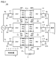
- FIG. 1 is a block diagram showing a main circuit configuration of a power conversion device according to an embodiment.
- the power conversion device according to the present embodiment can be typically applied to the uninterruptible power supply device 100.
- the uninterruptible power supply 100 is connected between the commercial AC power supply 5 and the load 6.
- the commercial AC power supply 5 supplies three-phase AC power to the uninterruptible power supply 100.
- the uninterruptible power supply 100 supplies three-phase AC power to the load 6.
- the commercial AC power supply 5 supplies commercial frequency three-phase AC voltages VR, VS, and VT to the uninterruptible power supply 100 via the R-phase line RL, S-phase line SL, and T-phase line TL.
- the uninterruptible power supply 100 receives the three-phase AC voltages VR, VS, and VT from the commercial AC power supply 5, and sets the commercial frequency three-phase AC voltages VU, VV, and VW to the U-phase line UL, V-phase line VL, and W-phase. Output to the load 6 via the line WL.
- the uninterruptible power supply 100 includes reactors L1 to L3, L11 to L13, capacitors C1 to C3, C11 to C13, power conversion units 21 to 23, DC positive bus PL, DC negative bus NL, battery 7, and control device 9. Be prepared.
- Reactors L1 to L3 and capacitors C1 to C3 form a three-phase LC filter circuit.
- This LC filter circuit is a low-pass filter and functions as an input filter for preventing the outflow of harmonics to the commercial AC power supply 5.
- Reactors L11 to L13 and capacitors C11 to C13 form a three-phase LC filter circuit.
- This LC filter circuit is a low-pass filter and functions as an output filter for preventing the outflow of harmonics to the load 6.
- the power conversion units 21 to 23 convert the three-phase AC voltage VR, VS, VT supplied from the commercial AC power supply 5 via the input filter into a DC voltage, and convert the DC voltage into the three-phase AC voltage VU, VV, VW. Convert to.
- the power conversion units 21 to 23 supply the three-phase AC voltages VU, VV, and VW to the load 6 via the output filter.
- the power conversion unit 21 includes a converter 1R, DC bus PL1, NL1, an inverter 2U, and fuses FP1, FP2, FN1, FN2.
- the power conversion unit 22 includes a converter 1S, DC bus PL2, NL2, an inverter 2V, and fuses FP3, FP4, FN3, and FN4.
- the power conversion unit 23 includes a converter 1T, DC bus PL3, NL3, an inverter 2WV, and fuses FP5, FP6, FN5, FN6.
- Each of the converters 1R, 1S, and 1T has an AC terminal AC2, a positive electrode DC terminal (that is, a high potential side DC terminal) BP1, and a negative electrode DC terminal (that is, a low potential side DC terminal) BN1.
- Each of the inverters 2U, 2V, and 2W has an AC terminal AC1, a positive electrode DC terminal BP2, and a negative electrode DC terminal BN2.
- the converters 1R, 1S, 1T and the inverters 2U, 2V, 2W correspond to one embodiment of the "power converter”.
- the converters 1R, 1S, 1T correspond to one embodiment of the "first power converter”.
- the inverters 2U, 2V, and 2W correspond to one embodiment of the "second power converter”.
- the AC terminal AC2 of the converter 1R receives the R-phase voltage VU from the R-phase line RL via the input filters (capacitor C1 and reactor L1).
- the converter 1R converts the R-phase voltage VR into a DC voltage and outputs the DC voltage between the DC terminals BP1 and BN1.
- the AC terminal AC2 of the converter 1S receives the S-phase voltage VS from the S-phase line SL via the input filters (capacitor C2 and reactor L2).
- the converter 1S converts the S-phase voltage VS into a DC voltage, and outputs the DC voltage between the DC terminals BP1 and BN1.
- the AC terminal AC2 of the converter 1T receives the T-phase voltage VT from the T-phase line RL via the input filters (capacitor C3 and reactor L3).
- the converter 1T converts the T-phase voltage VT into a DC voltage and outputs the DC voltage between the DC terminals BP1 and BN1.
- One terminal of the fuses FP1, FP3, and FP5 is connected to the positive electrode DC terminal BP1 of the converters 1R, 1S, and 1T, respectively.
- the other terminals of the fuses FP1, FP3, and FP5 are connected to the DC positive bus lines PL1 to PL3, respectively.
- One terminal of the fuses FN1, FN3, and FN5 is connected to the negative electrode DC terminal BN1 of the converters 1R, 1S, and 1T, respectively.
- the other terminals of the fuses FN1, FN3, and FN5 are connected to the DC negative bus lines NL1 to NL3, respectively.
- One terminal of the fuses FP2, FP4, and FP6 is connected to the DC positive bus lines PL1 to PL3, respectively.
- the other terminals of the fuses FP2, FP4, and FP6 are connected to the positive electrode DC terminals BP2 of the inverters 2U, 2V, and 2W, respectively.
- One terminal of the fuses FN2, FN4, and FN6 is connected to the DC negative bus NL1 to NL3, respectively.
- the other terminals of the fuses FN2, FN4, and FN6 are connected to the negative electrode DC terminals BN2 of the inverters 2U, 2V, and 2W, respectively.
- the DC terminals BP2 and BN2 of the inverter 2U receive a DC voltage from the converter 1R via the DC bus PL1 and NL1.
- the inverter 2U converts the DC voltage into a U-phase voltage VU and outputs the U-phase voltage VU to the AC terminal AC1.
- the DC terminals BP2 and BN2 of the inverter 2V receive a DC voltage from the converter 1S via the DC bus PL2 and NL2.
- the inverter 2V converts the DC voltage into a V-phase voltage VV, and outputs the V-phase voltage VV to the AC terminal AC1.
- the DC terminals BP2 and BN2 of the inverter 2W receive a DC voltage from the converter 1T via the DC bus PL3 and NL3.
- the inverter 2W converts the DC voltage into a W-phase voltage VW and outputs the W-phase voltage VW to the AC terminal AC1.
- the DC positive bus PL is connected to the DC positive bus PL1 to PL3.
- the DC negative bus NL is connected to the DC negative bus NL1 to NL3.
- the DC bus PL, NL receives the DC voltage generated by the converters 1R, 1S, 1T.
- the battery 7 is connected between the DC positive bus PL and the DC negative bus NL.
- the battery 7 corresponds to an embodiment of the "power storage device".
- the control device 9 controls the converters 1R, 1S, 1T and the inverters 2U, 2V, 2W in order to generate AC power to be supplied to the load 6 when the commercial AC power supply 5 is sound and when there is a power failure.
- the control device 9 is mainly composed of a microcomputer including, for example, a CPU (Central Processing Unit) and a storage unit such as a ROM (Read Only Memory) and a RAM (Random Access Memory).
- the control device 9 controls the converters 1R, 1S, 1T and the inverters 2U, 2V, 2W by the CPU reading the program stored in the ROM in advance into the RAM and executing the program.
- the control device 9 converts the three-phase AC voltage VR, VS, VT given from the commercial AC power supply 5 to the AC terminal AC2 into a DC voltage, and converts the DC voltage into a battery.
- the converters 1R, 1S, 1T and the inverters 2U, 2V, 2W are controlled so as to supply the voltage to 7 and convert the DC voltage into three-phase AC voltages VU, VV, VW and output them to the AC terminal AC1.
- the control device 9 stops the operation of the converters 1R, 1S, and 1T, and three-phases the DC voltage generated by the DC power supplied from the battery 7 to the DC terminals BP2 and BN2.
- the inverters 2U, 2V, and 2W are controlled so that they are converted into AC voltages VU, VV, and VW and output to the AC terminal AC1.
- circuit configuration of power converter In the uninterruptible power supply 100 shown in FIG. 1, a power converter having a common structure can be used for the converters 1R, 1S, 1T and the inverters 2U, 2V, 2W.
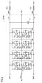
- FIG. 2 and 3 are block diagrams showing a circuit configuration of the power converter 10 according to the present embodiment.
- FIG. 2 shows a configuration example of the converter 1R using the power converter 10.
- the power converter 10 includes AC terminals AC1 and AC2, positive electrode DC terminals BP1 and BP2, and negative electrode DC terminals BN1 and BN2.
- the AC terminals AC1 and AC2 receive the AC voltage from the commercial AC power supply 5 or the load 6.
- the AC terminal AC2 is connected to the R-phase line RL and receives the R-phase voltage VR from the commercial AC power supply 5.
- the AC terminal AC2 corresponds to one embodiment of the "second AC terminal".
- the positive electrode DC terminals BP1 and BP2 are connected to one terminal of the fuse FP.
- the negative electrode DC terminals BN1 and BN2 are connected to one terminal of the fuse FN.
- the positive electrode DC terminal BP1 is connected to one terminal of the fuse FP1
- the negative electrode DC terminal BN1 is connected to one terminal of the fuse FN1.
- the positive electrode DC terminal BP1 corresponds to an embodiment of the “first positive electrode DC terminal”
- the positive electrode DC terminal BP2 corresponds to an embodiment of the “second positive electrode DC terminal”.
- the negative electrode DC terminal BN1 corresponds to an embodiment of the “first negative electrode DC terminal”
- the negative electrode DC terminal BN2 corresponds to an embodiment of the “second negative electrode DC terminal”.
- the power converter 10 further includes DC lines 14 and 16, AC lines 18, a plurality of semiconductor modules M1 to M4, and a capacitor 12.
- the DC line 14 is connected between the positive electrode DC terminal BP1 and the positive electrode DC terminal BP2.
- the DC line 16 is connected between the negative electrode DC terminal BN1 and the negative electrode DC terminal BN2.
- the AC line 18 is connected between the AC terminal AC1 and the AC terminal AC2.
- a plurality of semiconductor modules M1 to M4 are connected in parallel to each other between the DC line 14 and the DC line 16.
- the semiconductor modules M1 to M4 may be collectively referred to as the semiconductor module M.
- the number of semiconductor modules M is not limited to four, and can be changed to any number including a single module.
- the semiconductor module M has semiconductor switching elements Q1 and Q2, diodes D1 and D2, a collector terminal C1, an emitter terminal E2, a collector-emitter terminal C2E1, and control terminals G1, G2, E1, E2.
- Each of the semiconductor switching elements Q1 and Q2 is, for example, an IGBT (Insulated Gate Bipolar Transistor).
- the collector of the IGBT Q1 is connected to the collector terminal C1, and the emitter is connected to the collector of the IGBT Q2, the control terminal E1 and the collector-emitter terminal C2E1.
- the gate of the IGBT Q1 is connected to the control terminal G1.
- the emitter of the IGBT Q2 is connected to the emitter terminal E2 and the control terminal E2, and the gate is connected to the control terminal G2.
- the diode D1 is connected to the IGBT Q1 in antiparallel and the diode D2 is connected to the IGBTQ2 in antiparallel.
- the collector terminal C1 of the semiconductor module M is connected to the DC line 14, and the emitter terminal E2 is connected to the DC line 16.
- the collector-emitter terminal C2E1 of the semiconductor module M is connected to the AC line 18.
- the positive electrode of the capacitor 12 is connected to the DC line 14, and the negative electrode is connected to the DC line 16.
- the capacitor 12 has a plurality of capacitor unit CDs connected in parallel, as will be described later.
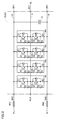
- FIG. 3 shows a configuration example of the inverter 2U using the power converter 10.
- the configuration example shown in FIG. 3 differs from the configuration example shown in FIG. 2 only in the connection of the DC bus PL1 and NL1 and the AC line.
- the AC terminal AC1 is connected to the U-phase line UL and outputs the U-phase voltage VU.
- the AC terminal AC1 corresponds to one embodiment of the "first AC terminal”.
- the positive electrode DC terminal BP2 is connected to one terminal of the fuse FP2, and the negative electrode DC terminal BN2 is connected to one terminal of the fuse FN2.
- FIG. 4 is a diagram schematically showing a connection relationship between the power converter 10 and the control device 9 according to the present embodiment.
- control terminals G1, G2, E1 and E2 of each semiconductor module M are connected to the control device 9.
- the collector terminal C1 of each semiconductor module M is connected to the DC line 14
- the emitter terminal E2 is connected to the DC line 16
- the collector-emitter terminal C2E1 is connected to the AC line 18.
- a plurality of capacitor unit CDs constituting the capacitor 12 are connected in parallel between the DC line 14 and the DC line 16.
- the number of capacitor unit CDs can be changed arbitrarily.
- the positive electrode DC terminals BP1 and BP2 are drawn out from the DC line 14 to the outside of the power converter 10.
- the negative electrode DC terminals BN1 and BN2 are drawn out from the DC line 16 to the outside of the power converter 10.
- the AC terminals AC1 and AC2 are drawn out from the AC line 18 to the outside of the power converter 10.
- the converter 1R and the inverter 2U can be realized by using the power converter 10 having a common configuration by changing the wiring connection.
- the productivity of the power conversion device can be increased, and as a result, the manufacturing cost can be reduced.
- repair and / or replacement is facilitated when a component fails, the cost of maintenance and inspection of the power conversion device can be reduced.
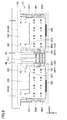
- FIG. 5 is a front view of the uninterruptible power supply 100 according to the present embodiment.
- FIG. 6 is a top view of the uninterruptible power supply 100 according to the present embodiment.
- the left-right direction (or the length direction) is the X direction
- the front-back direction (or the width direction) is the Z direction
- the up-down direction (or the thickness direction) is the Y direction.
- FIGS. 5 and 6 show an extracted portion related to the power conversion device according to the present embodiment.
- the components of the uninterruptible power supply 100 including the power conversion device shown in FIGS. 5 and 6, are housed inside a panel-shaped (rectangular parallelepiped) housing (not shown).
- the uninterruptible power supply 100 further includes stages 110, 120, 130 and a partition plate 140.
- the uninterruptible power supply 100 is configured by stacking stages 110, 120, and 130 on which power conversion units 21 to 23 are mounted, respectively, in the vertical direction (Y direction).
- the power conversion unit 23 is mounted on the lowermost stage 130
- the power conversion unit 22 is mounted on the middle stage 120
- the power conversion unit 21 is mounted on the uppermost stage 110.
- FIG. 6 shows a plan view of the uppermost power conversion unit 21.
- the partition plate 140 has a rectangular flat plate shape, and is installed so as to stand upright on the bottom surface of the housing of the uninterruptible power supply 100.
- the partition plate 140 has a first surface perpendicular to the Z direction and a second surface opposite to the first surface.
- the stages 110, 120, and 130 are fixed to the first surface of the partition plate 140.
- the DC positive bus PL and the DC negative bus NL are conductive members having a band shape.
- the conductive member is arranged on the second surface side of the partition plate 140 so as to extend in the Y direction. Through holes 150 and 160 are formed in the partition plate 140.
- Each of the stages 110, 120, and 130 has a rectangular flat plate shape, and has a first surface and a second surface opposite to the first surface.
- the converter 1R and the inverter 2U are arranged side by side in the length direction (X direction) on the first surface of the stage 110.
- the DC bus PL1, NL1 and the fuses FP1, FP2, FN1, FN2 are arranged in the space between the converter 1R and the inverter 2U.
- the converter 1S and the inverter 2V are arranged side by side in the length direction (X direction) on the first surface of the stage 120.
- the DC bus PL2, NL2 and the fuses FP3, FP4, FN3, FN2 are arranged in the space between the converter 1S and the inverter 2V.
- the converter 1T and the inverter 2W are arranged side by side in the length direction (X direction) on the first surface of the stage 130.
- the DC bus PL3, NL3 and the fuses FP5, FP6, FN5, FN6 are arranged in the space between the converter 1T and the inverter 2W.
- One end of the DC positive bus PL1, PL2, PL3 is connected to the DC positive bus PL through a through hole 150 formed in the partition plate 140.
- One end of the DC negative bus NL1, NL2, NL3 is connected to the DC negative bus NL through a through hole 160 formed in the partition plate 140.
- FIG. 7 is an external perspective view of the power converter 10.
- the power converter 10 includes a plurality of semiconductor modules M1 to M4, a plurality of capacitor unit CDs, a laminated bus bar 200, a housing 300, substrates 310 and 330, and a cover 320. ..
- the housing 300 has a rectangular parallelepiped shape, and its upper surface is open. An opening for introducing cooling air into the housing 300 is formed on one side surface of the housing 300 in the Z direction.
- the first substrate 310 is attached to the upper surface of the housing 300.
- the first substrate 310 has a rectangular flat plate shape.
- the first substrate 310 has a first surface facing the bottom surface of the housing 300 and a second surface opposite to the first surface.
- a heat sink (not shown) is fixed to the first surface.
- the heat sink has a base fixed to the first surface and fins protruding from the base.
- the heat sink is made of a metal with high thermal conductivity, such as aluminum or copper.
- the plurality of semiconductor modules M1 to M4 are arranged side by side in the length direction (X direction) on the second surface of the first substrate 310.
- the arrangement of the plurality of semiconductor modules M1 to M4 is not limited to this.
- the semiconductor module M includes semiconductor switching elements Q1 and Q2, diodes D1 and D2, collector terminal C1, emitter terminal E2, collector-emitter terminal C2E1, and control terminals G1, G2, E1. , E2.
- the semiconductor module M has, for example, a configuration in which semiconductor switching elements Q1 and Q2 and diodes D1 and D2 are mounted on a flat plate-shaped substrate.
- the semiconductor switching elements Q1 and Q2 and the diodes D1 and D2 are electrically connected by a bonding wire or a wiring layer.
- the semiconductor switching elements Q1 and Q2 and the diodes D1 and D2 are sealed with a resin together with a substrate, a bonding wire, a wiring layer, and the like.
- the resin is formed in a substantially rectangular shape.
- the collector terminal C1, the emitter terminal E2, and the collector-emitter terminal C2E1 are arranged so as to project parallel to each other from the surface of the resin having a substantially rectangular shape.
- the semiconductor module M is mounted on the laminated bus bar 200.
- a plurality of capacitor unit CDs are housed inside the housing 300.
- the plurality of capacitor unit CDs are arranged side by side so as to stand up on the bottom surface of the housing 300.
- the plurality of capacitor unit CDs constitute the capacitors 12 shown in FIGS. 2 and 3.
- the capacitor unit CD has a cylindrical portion and a positive electrode terminal and a negative electrode terminal provided at one end of the cylindrical portion. By connecting the positive electrode terminal and the negative electrode terminal to the laminated bus bar 200, the capacitor CD is mounted on the laminated bus bar 200.
- the plurality of semiconductor modules M and the plurality of capacitor CDs are electrically connected via the laminated bus bar 200.
- the laminated bus bar 200 constitutes DC lines 14 and 16 and AC lines 18 (see FIGS. 2 to 4).
- the laminated bus bar 200 has a substantially rectangular flat plate shape, and is arranged so as to face the bottom surface of the housing 300.
- the laminated bus bar 200 has a first surface 200A and a second surface 200B opposite to the first surface 200A.
- the second surface 200B faces the bottom surface of the housing 300.
- a cover 320 that covers a part of the first surface 200A is arranged above the thickness direction (Y direction) of the first surface 200A.
- the second substrate 320 is arranged on the cover 320.
- a control device 9 (see FIG. 1) and the like (see FIG. 1) (not shown) are mounted on the second substrate 320.
- FIG. 8 is a plan view showing the configuration of the laminated bus bar 200.
- the laminated bus bar 200 has a flat plate portion 210, AC terminals AC1 and AC2, positive electrode DC terminals BP1 and BP2, and negative electrode DC terminals BN1 and BN2.
- the flat plate portion 210 has a length direction (X direction), a width direction (Z direction) orthogonal to the length direction, and a thickness direction (Y direction) orthogonal to the length direction and the width direction.
- a plurality of through holes 211 to 215 penetrating in the thickness direction are formed in the flat plate portion 210.
- the through hole 211 (second through hole) is arranged at a position corresponding to the collector terminal C1 of the semiconductor module M.
- the through hole 212 (first through hole) is arranged at a position corresponding to the collector-emitter terminal C2E1 of the semiconductor module M.
- the through hole 213 (third through hole) is arranged at a position corresponding to the emitter terminal E2 of the semiconductor module M.
- the through hole 214 (fourth through hole) is arranged at a position corresponding to the positive electrode terminal of the capacitor unit CD.
- the through hole 215 (fifth through hole) is arranged at a position corresponding to the negative electrode terminal of the capacitor unit CD.
- Connection terminals (bolts, etc.) (not shown) are inserted into each through hole. With this connection terminal, the collector terminal C1 of the semiconductor module M, the collector-emitter terminal C2E1 and the emitter terminal E2, and the positive electrode terminal and the negative electrode terminal of the capacitor unit CD can be electrically connected to the laminated bus bar 200 at predetermined positions. can.
- FIG. 9 is an exploded perspective view of the flat plate portion 210 of the laminated bus bar 200.
- the flat plate portion 210 has a first conductive plate 220AC, a second conductive plate 220P, a third conductive plate 220N, and first to fourth insulating plates 215.
- the first to fourth insulating plates 215 and the first to third conductive plates 220AC, 220P, 220C are alternately laminated to form a laminated body.
- the laminated body includes a fourth insulating plate 215, a third conductive plate 220N, a third insulating plate 215, a second conductive plate 220P, a second insulating plate 215, and a first conductive plate from the bottom.
- the plate 220AC and the first insulating plate 215 are laminated in this order.
- a first AC terminal AC1 and a second AC terminal AC2 are formed on the first conductive plate 220AC.
- the first conductive plate 220AC constitutes an AC line 18 (see FIGS. 2 to 4).
- a first positive electrode DC terminal BP1 and a second positive electrode DC terminal BP2 are formed on the second conductive plate 220P.
- the second conductive plate 220P constitutes a DC line 14 (see FIGS. 2 to 4).
- a first negative electrode DC terminal BN1 and a second negative electrode DC terminal BN2 are formed on the third conductive plate 220N.
- the third conductive plate 220N constitutes a DC line 16 (see FIGS. 2 to 4).
- the first AC terminal AC1 protrudes from the first conductive plate 220AC in the length direction.
- the first positive electrode DC terminal BP1 projects in the length direction from the second conductive plate 220P.
- the first negative electrode DC terminal BN1 projects in the length direction from the third conductive plate 220N.
- Each of the first AC terminal AC1, the first positive electrode DC terminal BP1 and the first negative electrode DC terminal BN1 has a rectangular flat plate shape, and a connection hole 203 is formed by drilling.
- the second AC terminal AC2 protrudes from the first conductive plate 220AC in the length direction.
- the second positive electrode DC terminal BP2 projects in the length direction from the second conductive plate 220P.
- the second negative electrode DC terminal BN2 projects in the length direction from the third conductive plate 220N.
- Each of the second AC terminal AC2, the second positive electrode DC terminal BP2, and the second negative electrode DC terminal BN2 has a rectangular flat plate shape, and a connection hole 203 is formed by drilling.
- the first AC terminal AC1, the first positive electrode DC terminal BP1 and the first negative electrode DC terminal BN1 are from the third end 210C in the width direction of the flat plate portion 210 to the fourth end opposite to the third end 210C. They are arranged side by side in this order toward the end 210D.
- the second AC terminal AC2, the second negative electrode DC terminal BN2, and the second positive electrode DC terminal BP2 are arranged in this order from the third end 210C to the fourth end 210D in the width direction of the flat plate portion 210. Have been placed.
- the first AC terminal AC1 and the second AC terminal AC2 are arranged at positions facing each other in the length direction with the flat plate portion 210 interposed therebetween.
- the first positive electrode DC terminal BP1 and the second negative electrode DC terminal BN2 are arranged at positions facing each other in the length direction with the flat plate portion 210 interposed therebetween.
- the first negative electrode DC terminal BN1 and the second positive electrode DC terminal BP2 are arranged at positions facing each other in the length direction with the flat plate portion 210 interposed therebetween. That is, in the first end 210A and the second end 210B of the laminated bus bar 200, the order of the positive electrode DC terminal BP and the negative electrode DC terminal BN is reversed.
- the first power converter 10 (converter 1R) and the second power converter 10 (inverter 2U) are arranged side by side in the length direction (X direction). Specifically, the first end 210A of the laminated bus bar 200 of the first power converter 10 and the second end 210B of the laminated bus bar 200 of the second power converter 10 are in the length direction (X direction). The fourth end 210D of each laminated bus bar 200 is arranged in the width direction so as to be aligned with the length direction.
- the first positive electrode DC terminal BP1 of the first power converter 10 and the second negative electrode DC terminal BN2 of the second power converter 10 are arranged so as to face each other. become. Further, the first negative electrode DC terminal BN1 of the first power converter 10 and the second positive electrode DC terminal BP2 of the second power converter 10 are arranged so as to face each other.
- Each fuse has a substantially rectangular parallelepiped shape.
- Each fuse has a first terminal and a second terminal.
- the first terminal of the first fuse FP1 is connected to the first positive electrode DC terminal BP1 of the first power converter 10 (converter 1R) via the connecting member 162.
- the second terminal of the first fuse FP1 is connected to the first surface of the DC positive bus PL1 having a band shape.
- the first terminal of the second fuse FP2 is connected to the second positive electrode DC terminal BP2 of the second power converter 10 (inverter 2U) via the connecting member 152.
- the second terminal of the second fuse FP2 is connected to the second surface opposite to the first surface of the DC positive bus PL1.
- the first terminal of the third fuse FN1 is connected to the first negative electrode DC terminal BN1 of the first power converter 10 (converter 1R) via the connecting member 164.
- the second terminal of the third fuse FN1 is connected to the first surface of the DC negative bus NL1 having a band shape.
- the first terminal of the fourth fuse FN2 is connected to the second negative electrode DC terminal BN2 of the second power converter 10 (inverter 2U) via the connecting member 154.
- the second terminal of the fourth fuse FN2 is connected to the second surface opposite to the first surface of the DC negative bus NL1.
- Each of the connecting members 152, 154, 162, 164 is formed by bending a conductive member having a strip-shaped shape substantially vertically.
- a connection terminal such as a bolt can be used for connecting the first terminal of each fuse to the connecting member and connecting the second terminal of each fuse to the DC bus.
- the first fuse FP1 and the second fuse FP2 are arranged side by side in the length direction (X direction).
- the third fuse FN1 and the fourth fuse FN2 are arranged side by side in the length direction.
- the third fuse FN1 is arranged side by side in the thickness direction (Y direction) with respect to the first fuse FP1.
- the fourth fuse FN2 is arranged side by side in the thickness direction with respect to the second fuse FN2.
- the first fuse FP1 and the fourth fuse FN4 are arranged side by side in the length direction (X direction).
- the third fuse FN1 and the second fuse FP2 are arranged side by side in the length direction.
- FIG. 10 is a perspective view of the power conversion unit 21 as viewed from the first direction on the second power converter 10 (inverter 2U) side.
- FIG. 11 is a perspective view of the power conversion unit 21 as viewed from the second direction on the side of the first power converter 10 (converter 1R).
- the DC positive bus PL1 has a strip-shaped first conductive member extending in the width direction (Z direction).
- the DC negative bus NL1 has a strip-shaped second conductive member extending in the width direction.
- the first conductive member and the second conductive member are arranged side by side in the thickness direction (Y direction).
- the connection position of the first fuse FP1 with respect to the first conductive member and the connection position of the second fuse FP2 are deviated in the width direction.
- the connection position of the third fuse FN1 with respect to the second conductive member and the connection position of the fourth fuse FN2 are deviated in the width direction.
- the four fuses FP1, FP2, FN1 and FN2 are in the length direction (X direction), the width direction (Z direction) and the thickness direction (Y). It is arranged at a position where it does not overlap with each other in any of the directions). Therefore, as shown in FIG. 5, when the uninterruptible power supply 100 is viewed from the width direction, all four fuses FP1, FP2, FN1, and FN2 can be seen. According to this, the user can easily confirm whether or not each fuse is damaged, so that the quality of the uninterruptible power supply 100 can be improved.
- any one of the four fuses FP1, FP2, FN1 and FN2 is damaged, the damaged fuse can be easily removed and replaced with a new fuse. Therefore, workability at the time of installing and replacing the fuse can be improved.
- each of the DC positive bus PL1 and the DC negative bus NL1 can be formed by a conductive member having a simple band shape. According to this, since the conductive members constituting the DC bus PL1 and NL1 can be easily processed and assembled, the manufacturing cost of the power conversion device can be reduced.
- the laminated bus bar 200 even when a plurality of power converters included in the power converter are configured by the common power converter 10, two adjacent power converters are converted. It is possible to ensure the visibility of a plurality of fuses arranged in the space between the vessels and the workability at the time of installation. As a result, it is possible to realize common use of power converters with a simple configuration.
Landscapes
- Engineering & Computer Science (AREA)
- Power Engineering (AREA)
- Business, Economics & Management (AREA)
- Emergency Management (AREA)
- Inverter Devices (AREA)
Abstract
Description
図1は、実施の形態に従う電力変換装置の主回路構成を示すブロック図である。本実施の形態に従う電力変換装置は、代表的に無停電電源装置100に適用することができる。
図1に示した無停電電源装置100において、コンバータ1R,1S,1Tおよびインバータ2U,2V,2Wには、共通の構造を有する電力変換器を用いることができる。
次に、本実施の形態に従う電力変換器10の構成例および、電力変換器10を実装した電力変換装置(無停電電源装置100)の構成例について説明する。
図8を参照して、ラミネートブスバー200は、平板部210と、交流端子AC1,AC2と、正極直流端子BP1,BP2と、負極直流端子BN1,BN2とを有している。
Claims (10)
- 双方向に電力変換可能に構成された電力変換器に用いられるラミネートブスバーであって、
前記ラミネートブスバーは、長さ方向、前記長さ方向に直交する幅方向、および前記長さ方向と前記幅方向とに直交する厚さ方向とを有する平板部を有しており、
前記平板部は、
第1の交流端子および第2の交流端子が形成された第1の導電板と、
第1の正極直流端子および第2の正極直流端子が形成された第2の導電板と、
第1の負極直流端子および第2の負極直流端子が形成された第3の導電板と、
前記第1から第3の導電板に対して前記厚さ方向に交互に積層される第1から第5の絶縁板とを備え、
前記平板部の前記長さ方向の第1端部において、
前記第1の交流端子は、前記第1の導電板から前記長さ方向に突き出しており、
前記第1の正極直流端子は、前記第2の導電板から前記長さ方向に突き出しており、
前記第1の負極直流端子は、前記第3の導電板から前記長さ方向に突き出しており、かつ、
前記第1の交流端子、前記第1の正極直流端子および前記第1の負極直流端子は、前記平板部の前記幅方向の第3端部から、前記第3端部とは反対側の第4端部に向けてこの順に並べて配置され、
前記平板部の前記第1端部とは反対側の第2端部において、
前記第2の交流端子は、前記第1の導電板から前記長さ方向に突き出しており、
前記第2の正極直流端子は、前記第2の導電板から前記長さ方向に突き出しており、
前記第2の負極直流端子は、前記第3の導電板から前記長さ方向に突き出しており、かつ、
前記第2の交流端子、前記第2の負極直流端子および前記第2の正極直流端子は、前記平板部の前記第3端部から前記第4端部に向けてこの順に並べて配置される、ラミネートブスバー。 - 前記第1の正極直流端子と前記第2の負極直流端子とは、前記平板部を挟んで前記長さ方向に対向する位置に配置され、
前記第1の負極直流端子と前記第2の正極直流端子とは、前記平板部を挟んで前記長さ方向に対向する位置に配置される、請求項1に記載のラミネートブスバー。 - 前記第1の交流端子と前記第2の交流端子とは、前記平板部を挟んで前記長さ方向に対向する位置に配置される、請求項2に記載のラミネートブスバー。
- 第1端子、第2端子および交流端子を有する半導体モジュールと、
請求項1から3のいずれか1項に記載のラミネートブスバーとを備え、
前記平板部には、前記厚さ方向に貫通する複数の貫通孔が形成されており、
前記第1の導電板は、第1の貫通孔にて前記半導体モジュールの前記交流端子と接続され、
前記第2の導電板は、第2の貫通孔にて前記半導体モジュールの前記第1端子と接続され、
前記第3の導電板は、第3の貫通孔にて前記半導体モジュールの前記第2端子と接続される、電力変換器。 - 前記第1端子と前記第2端子との間に電気的に接続されるコンデンサをさらに備え、
前記第2の導電板は、第4の貫通孔にて前記コンデンサの正極端子と接続され、
前記第3の導電板は、第5の貫通孔にて前記コンデンサの負極端子と接続される、請求項4に記載の電力変換器。 - 第1の電力変換器と、
第2の電力変換器と、
前記第1の電力変換器および前記第2の電力変換器を搭載する平板状のステージとを備え、
前記第1の電力変換器は、第1の半導体モジュールと、前記第1の半導体モジュールに接続される第1のラミネートブスバーとを有しており、
前記第2の電力変換器は、第2の半導体モジュールと、前記第2の半導体モジュールに接続される第2のラミネートブスバーとを有しており、
前記第1および前記第2のラミネートブスバーの各々は、請求項1から3のいずれか1項に記載のラミネートブスバーにより構成され、
前記第1の電力変換器と前記第2の電力変換器とは、前記第1のラミネートブスバーの前記第1端部と、前記第2のラミネートブスバーの前記第2端部とが前記長さ方向に対向し、かつ、各々の前記第4端部が前記長さ方向に揃うように、前記長さ方向に並べて配置されており、
前記第1のラミネートブスバーの前記第1の正極直流端子と、前記第2のラミネートブスバーの前記第2の正極直流端子とを電気的に接続する直流正母線と、
前記第1のラミネートブスバーの前記第1の負極直流端子と、前記第2のラミネートブスバーの前記第2の負極直流端子とを電気的に接続する直流負母線と、
前記第1のラミネートブスバーの前記第1の正極直流端子と前記直流正母線との間に接続される第1のヒューズと、
前記直流正母線と前記第2のラミネートブスバーの前記第2の正極直流端子との間に接続される第2のヒューズと、
前記第1のラミネートブスバーの前記第1の負極直流端子と前記直流負母線との間に接続される第3のヒューズと、
前記直流負母線と前記第2のラミネートブスバーの前記第2の負極直流端子との間に接続される第4のヒューズとをさらに備え、
前記幅方向から見た平面視において、
前記第1のヒューズと前記第2のヒューズとは前記長さ方向に並べて配置され、
前記第3のヒューズは、前記第1のヒューズに対して前記厚さ方向に並べて配置され、
前記第4のヒューズは、前記第2のヒューズに対して前記厚さ方向に並べて配置され、
前記第3のヒューズと前記第4のヒューズとは前記長さ方向に並べて配置される、電力変換装置。 - 前記厚さ方向から見た平面視において、
前記第1のヒューズと前記第4のヒューズとは前記長さ方向に並べて配置され、
前記第3のヒューズと前記第2のヒューズとは前記長さ方向に並べて配置される、請求項6に記載の電力変換装置。 - 前記直流正母線は、前記幅方向に延びる帯状の第1の導電部材を含み、
前記直流負母線は、前記幅方向に延びる帯状の第2の導電部材を含み、
前記第1の導電部材と前記第2の導電部材とは前記厚さ方向に並べて配置される、請求項6または7に記載の電力変換装置。 - 前記第1の電力変換器は、コンバータであり、
前記第2の電力変換器は、インバータである、請求項6から8のいずれか1項に記載の電力変換装置。 - 請求項9に記載の電力変換装置と、
前記直流正母線と前記直流負母線との間に接続される電力貯蔵装置とを備え、
前記第1の電力変換器の前記第2の交流端子は交流電源に接続され、
前記第2の電力変換器の前記第1の交流端子は負荷に接続される、無停電電源装置。
Priority Applications (5)
| Application Number | Priority Date | Filing Date | Title |
|---|---|---|---|
| CN202080040818.XA CN113994559B (zh) | 2020-03-17 | 2020-03-17 | 层压母排、电力变换器、电力变换装置及不间断电源装置 |
| PCT/JP2020/011682 WO2021186538A1 (ja) | 2020-03-17 | 2020-03-17 | ラミネートブスバー、電力変換器、電力変換装置および無停電電源装置 |
| US17/610,541 US11901721B2 (en) | 2020-03-17 | 2020-03-17 | Laminated bus bar, power converter, power conversion device, and uninterruptible power supply device |
| JP2020541605A JP6955636B1 (ja) | 2020-03-17 | 2020-03-17 | ラミネートブスバー、電力変換器、電力変換装置および無停電電源装置 |
| KR1020217038715A KR102645318B1 (ko) | 2020-03-17 | 2020-03-17 | 래미네이트 버스 바, 전력 변환기, 전력 변환 장치 및 무정전 전원 장치 |
Applications Claiming Priority (1)
| Application Number | Priority Date | Filing Date | Title |
|---|---|---|---|
| PCT/JP2020/011682 WO2021186538A1 (ja) | 2020-03-17 | 2020-03-17 | ラミネートブスバー、電力変換器、電力変換装置および無停電電源装置 |
Publications (1)
| Publication Number | Publication Date |
|---|---|
| WO2021186538A1 true WO2021186538A1 (ja) | 2021-09-23 |
Family
ID=77770909
Family Applications (1)
| Application Number | Title | Priority Date | Filing Date |
|---|---|---|---|
| PCT/JP2020/011682 Ceased WO2021186538A1 (ja) | 2020-03-17 | 2020-03-17 | ラミネートブスバー、電力変換器、電力変換装置および無停電電源装置 |
Country Status (5)
| Country | Link |
|---|---|
| US (1) | US11901721B2 (ja) |
| JP (1) | JP6955636B1 (ja) |
| KR (1) | KR102645318B1 (ja) |
| CN (1) | CN113994559B (ja) |
| WO (1) | WO2021186538A1 (ja) |
Cited By (1)
| Publication number | Priority date | Publication date | Assignee | Title |
|---|---|---|---|---|
| WO2025134366A1 (ja) * | 2023-12-22 | 2025-06-26 | 株式会社Tmeic | インバータユニット及びインバータユニット用パッキン |
Families Citing this family (3)
| Publication number | Priority date | Publication date | Assignee | Title |
|---|---|---|---|---|
| JP7720822B2 (ja) * | 2022-10-04 | 2025-08-08 | 株式会社Tmeic | 電子部品モジュール |
| US12476555B2 (en) * | 2022-12-16 | 2025-11-18 | Bae Systems Controls Inc. | DC busbar system, laminated DC busbar and DC backplane with super low inductance |
| CN116613596B (zh) * | 2023-06-20 | 2024-03-19 | 格至控智能动力科技(上海)有限公司 | 叠层母排和功率装置 |
Citations (4)
| Publication number | Priority date | Publication date | Assignee | Title |
|---|---|---|---|---|
| JP2012165611A (ja) * | 2011-02-09 | 2012-08-30 | Mitsubishi Electric Corp | 半導体ユニット及び電力変換装置 |
| US20150340157A1 (en) * | 2014-05-23 | 2015-11-26 | Delta Electronics (Shanghai) Co., Ltd. | Direct-current capacitor module and laminated busbar structure thereof |
| WO2018116606A1 (ja) * | 2016-12-22 | 2018-06-28 | パナソニックIpマネジメント株式会社 | バスバーユニット及びモータ駆動装置 |
| JP2019517733A (ja) * | 2016-05-27 | 2019-06-24 | ゼネラル・エレクトリック・カンパニイ | 半導体パワーモジュール |
Family Cites Families (11)
| Publication number | Priority date | Publication date | Assignee | Title |
|---|---|---|---|---|
| CN102918479B (zh) * | 2010-05-31 | 2015-05-20 | 阿尔卑斯电气株式会社 | 输入装置 |
| JP6198941B2 (ja) | 2014-05-07 | 2017-09-20 | 株式会社日立製作所 | 電力変換装置 |
| US11205919B2 (en) | 2015-09-30 | 2021-12-21 | Toshiba Mitsubishi-Electric Industrial Systems Corporation | Uninterruptible power supply system |
| CN105322484B (zh) * | 2015-12-08 | 2017-04-26 | 华中科技大学 | 一种应用于高压固态电力电子开关的叠层母排 |
| JP2017127152A (ja) * | 2016-01-15 | 2017-07-20 | 住友重機械工業株式会社 | 電力変換装置およびそれを用いたショベルならびにラミネートブスバー |
| JP2018067998A (ja) * | 2016-10-18 | 2018-04-26 | 三菱電機株式会社 | 電力変換装置 |
| JP6824840B2 (ja) | 2017-07-11 | 2021-02-03 | 東芝三菱電機産業システム株式会社 | ラミネートブスバー |
| US10608423B2 (en) * | 2018-04-26 | 2020-03-31 | Sf Motors, Inc. | Electric vehicle inverter module laminated bus bar |
| CN110416947A (zh) * | 2018-12-10 | 2019-11-05 | 西安中车永电电气有限公司 | 一种喷涂式叠层铜排及其制备工艺 |
| CN209981978U (zh) * | 2018-12-10 | 2020-01-21 | 西安中车永电电气有限公司 | 一种喷涂式叠层铜排 |
| US11335649B2 (en) * | 2019-05-20 | 2022-05-17 | Virginia Tech Intellectual Properties, Inc. | Low impedance multi-conductor layered bus structure with shielding |
-
2020
- 2020-03-17 US US17/610,541 patent/US11901721B2/en active Active
- 2020-03-17 KR KR1020217038715A patent/KR102645318B1/ko active Active
- 2020-03-17 CN CN202080040818.XA patent/CN113994559B/zh active Active
- 2020-03-17 WO PCT/JP2020/011682 patent/WO2021186538A1/ja not_active Ceased
- 2020-03-17 JP JP2020541605A patent/JP6955636B1/ja active Active
Patent Citations (4)
| Publication number | Priority date | Publication date | Assignee | Title |
|---|---|---|---|---|
| JP2012165611A (ja) * | 2011-02-09 | 2012-08-30 | Mitsubishi Electric Corp | 半導体ユニット及び電力変換装置 |
| US20150340157A1 (en) * | 2014-05-23 | 2015-11-26 | Delta Electronics (Shanghai) Co., Ltd. | Direct-current capacitor module and laminated busbar structure thereof |
| JP2019517733A (ja) * | 2016-05-27 | 2019-06-24 | ゼネラル・エレクトリック・カンパニイ | 半導体パワーモジュール |
| WO2018116606A1 (ja) * | 2016-12-22 | 2018-06-28 | パナソニックIpマネジメント株式会社 | バスバーユニット及びモータ駆動装置 |
Cited By (1)
| Publication number | Priority date | Publication date | Assignee | Title |
|---|---|---|---|---|
| WO2025134366A1 (ja) * | 2023-12-22 | 2025-06-26 | 株式会社Tmeic | インバータユニット及びインバータユニット用パッキン |
Also Published As
| Publication number | Publication date |
|---|---|
| JP6955636B1 (ja) | 2021-10-27 |
| US20220216724A1 (en) | 2022-07-07 |
| US11901721B2 (en) | 2024-02-13 |
| KR20220002518A (ko) | 2022-01-06 |
| CN113994559B (zh) | 2023-06-30 |
| JPWO2021186538A1 (ja) | 2021-09-23 |
| CN113994559A (zh) | 2022-01-28 |
| KR102645318B1 (ko) | 2024-03-07 |
Similar Documents
| Publication | Publication Date | Title |
|---|---|---|
| JP6955636B1 (ja) | ラミネートブスバー、電力変換器、電力変換装置および無停電電源装置 | |
| US10141861B2 (en) | Power conversion unit, power converter and method of manufacturing power converter | |
| CN101741227B (zh) | 水冷型三相二极管箝位型三电平逆变功率模块 | |
| US8576528B2 (en) | Matrix converter | |
| JP2013055840A (ja) | 電力変換装置 | |
| RU2702218C1 (ru) | Силовая ячейка с печатными платами и развязкой и многоячеечный источник электропитания среднего напряжения | |
| JP2012165611A (ja) | 半導体ユニット及び電力変換装置 | |
| WO2017168518A1 (ja) | 電力変換装置 | |
| CN109412431B (zh) | 叠层铜排及三相大功率逆变器 | |
| CN215222037U (zh) | 汇流连接装置、npc三电平功率组件及npc三电平变流器 | |
| JP7684285B2 (ja) | モジュラースイッチングセル | |
| JP2017085896A (ja) | 3レベル電力変換装置 | |
| JP7512536B2 (ja) | 電力変換装置 | |
| EP4518597A1 (en) | Power assembly apparatus and liquid cooling converter thereof | |
| CN109088547A (zh) | 用于开关模块的电容器基板单元 | |
| EP3817215B1 (en) | Power conversion device | |
| CN209472561U (zh) | 叠层铜排及三相大功率逆变器 | |
| JP7570528B2 (ja) | 電力変換装置 | |
| JP7101921B1 (ja) | 電力変換システム | |
| CN213661429U (zh) | 一种集成电容的分体式四象限功率单元结构 | |
| WO2018177732A1 (en) | 3-level power module | |
| JP2022179369A (ja) | 電力変換装置 | |
| RU2190919C2 (ru) | Силовая цепь электрического силового преобразователя | |
| JP2021061692A (ja) | 電力変換装置 | |
| JP6760883B2 (ja) | 電力変換装置 |
Legal Events
| Date | Code | Title | Description |
|---|---|---|---|
| ENP | Entry into the national phase |
Ref document number: 2020541605 Country of ref document: JP Kind code of ref document: A |
|
| 121 | Ep: the epo has been informed by wipo that ep was designated in this application |
Ref document number: 20925761 Country of ref document: EP Kind code of ref document: A1 |
|
| ENP | Entry into the national phase |
Ref document number: 20217038715 Country of ref document: KR Kind code of ref document: A |
|
| NENP | Non-entry into the national phase |
Ref country code: DE |
|
| 122 | Ep: pct application non-entry in european phase |
Ref document number: 20925761 Country of ref document: EP Kind code of ref document: A1 |