WO2021182087A1 - コネクタ装置 - Google Patents
コネクタ装置 Download PDFInfo
- Publication number
- WO2021182087A1 WO2021182087A1 PCT/JP2021/006561 JP2021006561W WO2021182087A1 WO 2021182087 A1 WO2021182087 A1 WO 2021182087A1 JP 2021006561 W JP2021006561 W JP 2021006561W WO 2021182087 A1 WO2021182087 A1 WO 2021182087A1
- Authority
- WO
- WIPO (PCT)
- Prior art keywords
- movable terminal
- connecting member
- movable
- hole
- terminal portion
- Prior art date
- Legal status (The legal status is an assumption and is not a legal conclusion. Google has not performed a legal analysis and makes no representation as to the accuracy of the status listed.)
- Ceased
Links
Images
Classifications
-
- H—ELECTRICITY
- H01—ELECTRIC ELEMENTS
- H01R—ELECTRICALLY-CONDUCTIVE CONNECTIONS; STRUCTURAL ASSOCIATIONS OF A PLURALITY OF MUTUALLY-INSULATED ELECTRICAL CONNECTING ELEMENTS; COUPLING DEVICES; CURRENT COLLECTORS
- H01R13/00—Details of coupling devices of the kinds covered by groups H01R12/70 or H01R24/00 - H01R33/00
- H01R13/62—Means for facilitating engagement or disengagement of coupling parts or for holding them in engagement
- H01R13/629—Additional means for facilitating engagement or disengagement of coupling parts, e.g. aligning or guiding means, levers, gas pressure electrical locking indicators, manufacturing tolerances
- H01R13/631—Additional means for facilitating engagement or disengagement of coupling parts, e.g. aligning or guiding means, levers, gas pressure electrical locking indicators, manufacturing tolerances for engagement only
- H01R13/6315—Additional means for facilitating engagement or disengagement of coupling parts, e.g. aligning or guiding means, levers, gas pressure electrical locking indicators, manufacturing tolerances for engagement only allowing relative movement between coupling parts, e.g. floating connection
-
- H—ELECTRICITY
- H01—ELECTRIC ELEMENTS
- H01R—ELECTRICALLY-CONDUCTIVE CONNECTIONS; STRUCTURAL ASSOCIATIONS OF A PLURALITY OF MUTUALLY-INSULATED ELECTRICAL CONNECTING ELEMENTS; COUPLING DEVICES; CURRENT COLLECTORS
- H01R12/00—Structural associations of a plurality of mutually-insulated electrical connecting elements, specially adapted for printed circuits, e.g. printed circuit boards [PCB], flat or ribbon cables, or like generally planar structures, e.g. terminal strips, terminal blocks; Coupling devices specially adapted for printed circuits, flat or ribbon cables, or like generally planar structures; Terminals specially adapted for contact with, or insertion into, printed circuits, flat or ribbon cables, or like generally planar structures
- H01R12/70—Coupling devices
- H01R12/91—Coupling devices allowing relative movement between coupling parts, e.g. floating or self aligning
-
- H—ELECTRICITY
- H01—ELECTRIC ELEMENTS
- H01R—ELECTRICALLY-CONDUCTIVE CONNECTIONS; STRUCTURAL ASSOCIATIONS OF A PLURALITY OF MUTUALLY-INSULATED ELECTRICAL CONNECTING ELEMENTS; COUPLING DEVICES; CURRENT COLLECTORS
- H01R12/00—Structural associations of a plurality of mutually-insulated electrical connecting elements, specially adapted for printed circuits, e.g. printed circuit boards [PCB], flat or ribbon cables, or like generally planar structures, e.g. terminal strips, terminal blocks; Coupling devices specially adapted for printed circuits, flat or ribbon cables, or like generally planar structures; Terminals specially adapted for contact with, or insertion into, printed circuits, flat or ribbon cables, or like generally planar structures
- H01R12/70—Coupling devices
- H01R12/71—Coupling devices for rigid printing circuits or like structures
- H01R12/712—Coupling devices for rigid printing circuits or like structures co-operating with the surface of the printed circuit or with a coupling device exclusively provided on the surface of the printed circuit
- H01R12/716—Coupling device provided on the PCB
-
- H—ELECTRICITY
- H01—ELECTRIC ELEMENTS
- H01R—ELECTRICALLY-CONDUCTIVE CONNECTIONS; STRUCTURAL ASSOCIATIONS OF A PLURALITY OF MUTUALLY-INSULATED ELECTRICAL CONNECTING ELEMENTS; COUPLING DEVICES; CURRENT COLLECTORS
- H01R13/00—Details of coupling devices of the kinds covered by groups H01R12/70 or H01R24/00 - H01R33/00
- H01R13/648—Protective earth or shield arrangements on coupling devices, e.g. anti-static shielding
- H01R13/655—Protective earth or shield arrangements on coupling devices, e.g. anti-static shielding with earth brace
-
- H—ELECTRICITY
- H01—ELECTRIC ELEMENTS
- H01R—ELECTRICALLY-CONDUCTIVE CONNECTIONS; STRUCTURAL ASSOCIATIONS OF A PLURALITY OF MUTUALLY-INSULATED ELECTRICAL CONNECTING ELEMENTS; COUPLING DEVICES; CURRENT COLLECTORS
- H01R24/00—Two-part coupling devices, or either of their cooperating parts, characterised by their overall structure
- H01R24/38—Two-part coupling devices, or either of their cooperating parts, characterised by their overall structure having concentrically or coaxially arranged contacts
- H01R24/40—Two-part coupling devices, or either of their cooperating parts, characterised by their overall structure having concentrically or coaxially arranged contacts specially adapted for high frequency
- H01R24/50—Two-part coupling devices, or either of their cooperating parts, characterised by their overall structure having concentrically or coaxially arranged contacts specially adapted for high frequency mounted on a PCB [Printed Circuit Board]
-
- H—ELECTRICITY
- H01—ELECTRIC ELEMENTS
- H01R—ELECTRICALLY-CONDUCTIVE CONNECTIONS; STRUCTURAL ASSOCIATIONS OF A PLURALITY OF MUTUALLY-INSULATED ELECTRICAL CONNECTING ELEMENTS; COUPLING DEVICES; CURRENT COLLECTORS
- H01R24/00—Two-part coupling devices, or either of their cooperating parts, characterised by their overall structure
- H01R24/38—Two-part coupling devices, or either of their cooperating parts, characterised by their overall structure having concentrically or coaxially arranged contacts
- H01R24/40—Two-part coupling devices, or either of their cooperating parts, characterised by their overall structure having concentrically or coaxially arranged contacts specially adapted for high frequency
- H01R24/54—Intermediate parts, e.g. adapters, splitters or elbows
-
- H—ELECTRICITY
- H01—ELECTRIC ELEMENTS
- H01R—ELECTRICALLY-CONDUCTIVE CONNECTIONS; STRUCTURAL ASSOCIATIONS OF A PLURALITY OF MUTUALLY-INSULATED ELECTRICAL CONNECTING ELEMENTS; COUPLING DEVICES; CURRENT COLLECTORS
- H01R12/00—Structural associations of a plurality of mutually-insulated electrical connecting elements, specially adapted for printed circuits, e.g. printed circuit boards [PCB], flat or ribbon cables, or like generally planar structures, e.g. terminal strips, terminal blocks; Coupling devices specially adapted for printed circuits, flat or ribbon cables, or like generally planar structures; Terminals specially adapted for contact with, or insertion into, printed circuits, flat or ribbon cables, or like generally planar structures
- H01R12/70—Coupling devices
- H01R12/71—Coupling devices for rigid printing circuits or like structures
- H01R12/72—Coupling devices for rigid printing circuits or like structures coupling with the edge of the rigid printed circuits or like structures
- H01R12/73—Coupling devices for rigid printing circuits or like structures coupling with the edge of the rigid printed circuits or like structures connecting to other rigid printed circuits or like structures
-
- H—ELECTRICITY
- H01—ELECTRIC ELEMENTS
- H01R—ELECTRICALLY-CONDUCTIVE CONNECTIONS; STRUCTURAL ASSOCIATIONS OF A PLURALITY OF MUTUALLY-INSULATED ELECTRICAL CONNECTING ELEMENTS; COUPLING DEVICES; CURRENT COLLECTORS
- H01R13/00—Details of coupling devices of the kinds covered by groups H01R12/70 or H01R24/00 - H01R33/00
- H01R13/62—Means for facilitating engagement or disengagement of coupling parts or for holding them in engagement
- H01R13/629—Additional means for facilitating engagement or disengagement of coupling parts, e.g. aligning or guiding means, levers, gas pressure electrical locking indicators, manufacturing tolerances
-
- H—ELECTRICITY
- H01—ELECTRIC ELEMENTS
- H01R—ELECTRICALLY-CONDUCTIVE CONNECTIONS; STRUCTURAL ASSOCIATIONS OF A PLURALITY OF MUTUALLY-INSULATED ELECTRICAL CONNECTING ELEMENTS; COUPLING DEVICES; CURRENT COLLECTORS
- H01R2105/00—Three poles
Definitions
- the first connector 10 includes one first housing 11 and a plurality of first terminal portions 16.
- the upper surface of the first housing 11 is fixed to the first circuit board B, and the upper ends of the plurality of first terminal portions 16 are printed on the first circuit board B. It is connected to a circuit (not shown).
- the first housing 11 is a single component made of synthetic resin having a rectangular first terminal holding portion 12 and a rectangular guiding portion 14.
- the first terminal holding portion 12 is formed with a plurality of (three in the first embodiment) first terminal accommodating chambers 13 penetrating the first terminal holding portion 12 vertically.
- the first terminal accommodating chamber 13 has a circular shape.
- the plurality of first terminal accommodating chambers 13 are arranged so as to be lined up in a row in the left-right direction.
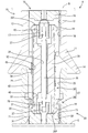
- the first terminal portion 16 includes a first inner conductor 17 made of metal, a first dielectric 18 made of synthetic resin, and a first outer conductor 19 made of metal.
- the first inner conductor 17 has a tubular shape with its axis oriented parallel to the mating direction of both connectors 10 and 20.
- the first dielectric 18 has a disk shape having a central hole. The upper end of the first inner conductor 17 is fitted into the central hole of the first dielectric 18, and the lower end of the first inner conductor 17 projects downward from the first dielectric 18.
- the first outer conductor 19 has a cylindrical shape that coaxially surrounds the first inner conductor 17 and the first dielectric 18, and is fitted to the inner peripheral surface of the first terminal accommodating chamber 13.
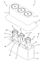
- the second connector 20 includes a second housing 21 and a plurality of second terminal portions 27 having the same number as the first terminal portion 16.
- Each second terminal portion 27 includes one fixed terminal portion 28 and one movable terminal portion 35.
- the second housing 21 is a single component made of synthetic resin having a rectangular second terminal holding portion 22 and a rectangular peripheral wall portion 24.
- the second terminal holding portion 22 is formed with a plurality of second terminal accommodating chambers 23 having the same number as the second terminal portion 27.
- the second terminal accommodating chamber 23 has a form in which the second terminal holding portion 22 is vertically penetrated.
- the second terminal accommodating chamber 23 has a circular shape.
- the plurality of second terminal accommodating chambers 23 are arranged so as to be lined up in a row in the left-right direction.
- the peripheral wall portion 24 has a form protruding upward from the outer peripheral edge at the upper end of the second terminal holding portion 22 in parallel with the fitting direction of both connectors 10 and 20. In a plan view, the peripheral wall portion 24 surrounds all of the plurality of second terminal accommodating chambers 23. Of the second housing 21, the space defined by the peripheral wall portion 24 above the second terminal holding portion 22 functions as a swinging space 25. The swing space 25 surrounded by the peripheral wall portion 24 is open above the second housing 21, that is, toward the first connector 10.
- the fixed terminal portion 28 includes a fixed inner conductor 29 made of metal, a fixed dielectric 30 made of synthetic resin, and a fixed outer conductor 31 made of metal.
- the fixed inner conductor 29 is the same component as the first inner conductor 17.
- the fixed inner conductor 29 is arranged upside down from the first inner conductor 17 in the axial direction.
- the fixed dielectric 30 is the same component as the first dielectric 18, and is arranged upside down from the first dielectric 18 in the axial direction.
- the lower end of the fixed inner conductor 29 is fitted into the central hole of the fixed dielectric 30, and the upper end of the fixed inner conductor 29 projects upward from the fixed dielectric 30.
- the fixed outer conductor 31 has a cylindrical shape that coaxially surrounds the fixed inner conductor 29 and the fixed dielectric 30, and is fitted to the inner peripheral surface of the second terminal accommodating chamber 23.
- the space above the fixed dielectric 30 in the fixed outer conductor 31 functions as a support space 32 open upward.
- the upper end portion of the fixed inner conductor 29 projects upward.
- Each support space 32 communicates with the swing space 25.
- a continuous diameter-reduced portion 33 is formed on the inner circumference of the upper end portion of the fixed outer conductor 31 over the entire circumference.
- the reduced diameter portion 33 is arranged in the support space 32 and has a shape that bulges inward in the radial direction.
- the movable terminal portion 35 has an elongated shape as a whole. Both ends of the movable terminal portion 35 in the axial direction have symmetry that gives the same shape when the movable terminal portion 35 is inverted.
- the movable terminal portion 35 is a member including a movable inner conductor 36 made of metal, a movable dielectric 38 made of synthetic resin, and a movable outer conductor 42 made of metal.
- the movable inner conductor 36 has an elongated tubular shape in the axial direction of the movable terminal portion 35.
- a pair of elastic claw pieces 37 that can be elastically deformed in the radial direction are formed at both ends of the movable inner conductor 36 in the axial direction.
- the movable terminal portion 35 is separated from the fixed terminal portion 28. Even if the movable terminal portion 35 is turned upside down so as to project downward from the fixed terminal portion 28, the locked state of the enlarged diameter portion 44 and the reduced diameter portion 33 is maintained.
- the movable terminal portion 35 can swing independently of the other movable terminal portions 35 with the contact portion between the base end portion 35P and the fixed terminal portion 28 as a fulcrum. Even if the movable terminal portion 35 swings in the front-rear direction or the left-right direction with respect to the fixed terminal portion 28, the locked state of the enlarged diameter portion 44 and the reduced diameter portion 33 is maintained.
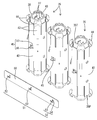
- the connecting member 50 is formed with a hooking portion 51 for connecting a plurality of movable terminal portions 35.
- the hook portion 51 is composed of a plurality of slit-shaped connecting holes 52 having the same number as the movable terminal portion 35.
- the plurality of connecting holes 52 are arranged at the same pitch as the plurality of movable terminal portions 35 in the left-right direction.
- the connecting hole 52 penetrates the connecting member 50 in the plate thickness direction, that is, in a direction perpendicular to both the length direction (vertical direction) of the movable terminal portion 35 and the arrangement direction (horizontal direction) of the plurality of movable terminal portions 35. doing.
- the shape of the connecting hole 52 is a mirror-inverted L-shape when the connecting member 50 is viewed from the outer surface side.
- the connecting hole 52 has a slit-shaped holding hole 53 and a slit-shaped mounting hole 54.
- the holding hole portion 53 extends in parallel with the arrangement direction (left-right direction) of the plurality of movable terminal portions 35.
- the mounting hole portion 54 extends in parallel with the length direction (vertical direction) of the movable terminal portion 35.
- One end (rear end) of the holding hole 53 and one end (lower end) of the mounting hole 54 communicate with each other at a right angle.
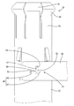
- the base 46 and the retaining portion 47 are individually held by an automatic machine, a jig, or the like, and the retaining portion 47 is displaced by 90 ° relative to the base 46.
- the base 46 is fixed by an automatic machine, a jig, or the like, even if a reaction force acts from the retaining portion 47 side to the base 46 side when bending the retaining portion 47, the reaction force is the movable outer conductor. It is not transmitted to 42. Therefore, it is possible to prevent the movable outer conductor 42 from being deformed when the retaining portion 47 is bent.
- the base portion 46 and the retaining portion 47 When the retaining portion 47 is displaced, as shown in FIGS. 4 and 5, the base portion 46 and the retaining portion 47 have a shape extending in a straight line in the left-right direction.
- the protrusion 45 is plastically deformed so that the retaining portion 47 and the base portion 46 are in a straight line, the retaining portion 47 is displaced to a position where it is turned 90 ° with respect to the mounting hole portion 54, and the outer surface of the connecting member 50 is displaced.
- the connecting hole 52 faces a non-corresponding region. That is, the tip portion of the retaining portion 47 on the side opposite to the base portion 46 and the boundary line 48 is located outside the connecting hole 52 and is located so as to face the outer surface of the connecting member 50.
- a clearance is secured between the base portion 46 and the hole edge portion of the holding hole portion 53, but the clearance is the minimum necessary space for allowing the movable terminal portion 35 and the connecting hole 52 to tilt. Is. Therefore, even if the connecting member 50 attempts to displace the movable terminal portion 35 in the two-dimensional direction including the horizontal direction and the vertical direction, the relative displacement amount between the connecting member 50 and the movable terminal portion 35 is not large.
- the connecting member 50 After attaching the connecting member 50 to the plurality of movable terminal portions 35 and connecting the plurality of movable terminal portions 35, the plurality of movable terminal portions 35 are attached to the fixed terminal portion 28.
- the base end portion 35P of the movable terminal portion 35 is inserted into the swing space 25 and fitted into the support space 32 of the fixed terminal portion 28.
- the connecting member 50 may be attached to the second housing 21 after the movable terminal portion 35 is attached to the fixed terminal portion 28.
- the amount of displacement of the connecting member 50 when the movable terminal portion 35 is tilted increases as the contact position of the connecting member 50 approaches the tip portion 35T of the movable terminal portion 35.
- the pressing force generated between the movable terminal portion 35 and the connecting member 50 is such that the contact position of the connecting member 50 is the movable terminal.
- the connecting member 50 since the contact position of the connecting member 50 is an intermediate position between the base end portion 35P and the tip end portion 35T, the connecting member 50 is connected to the movable terminal portion 35 while suppressing the displacement amount of the connecting member 50 when the movable terminal portion 35 is tilted.
- the pressing force generated between the member 50 and the member 50 can be reduced.
- the tip 35T of any of the movable terminal portions 35 is guided. It comes into contact with the inner surface of the portion 14.
- the tip portion 35T of the movable terminal portion 35 is in sliding contact with the inclined inner surface of the guide portion 14, so that the tip portions 35T of all the movable terminal portions 35 are brought into contact with each other. , While changing the swing angle all at once, it is guided to the connection position with the first terminal portion 16. During this time, the base end portion 35P of the movable terminal portion 35 swings in the swing space 25, and the tip end portion 35T of the movable terminal portion 35 swings inside the guide portion 14.
- the connector device A of this embodiment includes a first connector 10 mounted on the first circuit board B and a second connector 20 mounted on the second circuit board C.
- the first connector 10 has a plurality of first terminal portions 16 in a form in which the first inner conductor 17 is surrounded by the first outer conductor 19.
- the second connector 20 has a first housing 11 mounted on the second circuit board C, a plurality of fixed terminal portions 28, and a plurality of movable terminal portions 35.
- the fixed terminal portion 28 is attached to the second housing 21 and connected to the second circuit board C.
- the movable terminal portion 35 can swing individually with the plurality of fixed terminal portions 28 as fulcrums.
- the movable terminal portion 35 is individually connected to the plurality of first terminal portions 16.
- the connecting member 50 has a hooking portion 51 that is hooked on the plurality of movable terminal portions 35, and swings the plurality of movable terminal portions 35 integrally.
- the movable terminal portion 35 is a separate member from the fixed terminal portion 28.
- the movable outer conductor 42 of the movable terminal portion 35 has a diameter-expanded portion 44.
- the fixed outer conductor 31 of the fixed terminal portion 28 has a reduced diameter portion 33.
- the enlarged diameter portion 44 and the reduced diameter portion 33 function as support portions that swingably support the movable terminal portion 35 with respect to the fixed terminal portion 28. According to this configuration, even if the second connector 20 is oriented so that the movable terminal portion 35 projects downward from the fixed terminal portion 28, the movable terminal portion 35 can be held by the fixed terminal portion 28.
- the movable terminal portion 35 has a shape that protrudes from the fixed terminal portion 28 toward the front side of the second housing 21 and extends in an elongated direction along the protruding direction.
- the second housing 21 has a peripheral wall portion 24 that surrounds the plurality of movable terminal portions 35.
- the connecting member 50 is arranged in a region surrounded by the peripheral wall portion 24 in the fitting direction view of the second housing 21 as viewed from the first terminal portion 16. According to this configuration, the connector device A can be miniaturized in the fitting direction view.
- the plate-shaped connecting member 50 is arranged so that the plate thickness direction of the connecting member 50 faces the same direction as the facing direction between the outer surface of the movable terminal portion 35 and the inner surface of the peripheral wall portion 24.
- the plate thickness direction of the connecting member 50 is set in a direction orthogonal to the arrangement direction of the movable terminal portions 35. According to this configuration, since the connecting member 50 can be accommodated in the gap between the movable terminal portion 35 and the inner surface of the peripheral wall portion 24, the connector device can be further miniaturized in the fitting direction view.
- the hooking portion 51 is composed of a plurality of connecting holes 52 in a form penetrating the connecting member 50.
- a protrusion 45 that penetrates the connecting hole 52 is formed on the outer peripheral surface of the movable terminal portion 35.
- the protrusion 45 is made of a plastically deformable plate material.
- the protrusion 45 is formed with a base 46 and a retaining portion 47.
- the base portion 46 is connected to the outer peripheral surface of the movable terminal portion 35, penetrates the connecting hole 52, and projects toward the outer surface side of the connecting member 50.
- the retaining portion 47 extends from the base portion 46 and is arranged so as to face a region of the outer surface of the connecting member 50 that does not correspond to the connecting hole 52. That is, the retaining portion 47 is arranged so as to face the outer surface of the connecting member 50 and to be hooked on the outer surface of the connecting member 50.
- the boundary line 48 between the base portion 46 and the retaining portion 47 extends in a direction orthogonal to the outer surface of the connecting member 50.
- the protrusion 45 formed into the same shape as the connecting hole 52 is passed through the connecting hole 52, and then the retaining portion 47 is bent with respect to the base portion 46 to plastically deform the protrusion 45.
- the connecting member 50 is assembled to the movable terminal portion 35.
- the retaining portion 47 can be bent while the base portion 46 is fixed with a jig or the like, so that the bending force applied to the retaining portion 47 is applied to the movable terminal portion 35. It does not act on the outer peripheral surface of the movable outer conductor 42. This makes it possible to prevent deformation of the outer peripheral surface of the movable outer conductor 42.
- a clearance is provided between the protrusion 45 and the edge of the connecting hole 52 to allow the connecting member 50 and the movable terminal 35 to be relatively tilted. According to this configuration, when the movable terminal portion 35 swings, the protruding portion 45 does not strongly interfere with the hole edge portion of the connecting hole 52, so that the hole edge portion of the protruding portion 45 or the connecting hole 52 Deformation can be prevented.
- the outer peripheral surface of the movable terminal portion 35 is composed of a movable outer conductor 42.
- the connecting member 50 has conductivity and is in contact with a plurality of movable outer conductors 42. According to this configuration, it is possible to prevent a potential difference from occurring between the plurality of movable outer conductors 42, so that the grounding performance is improved.
- the present invention is not limited to the examples described in the above description and drawings, but is shown by the scope of claims.
- the present invention includes the meaning equivalent to the scope of claims and all modifications within the scope of claims, and is intended to include the following embodiments.
- the connecting holes are L-shaped, but the shape of the connecting holes may be V-shaped, J-shaped, or the like.
- the protrusion formed on the movable terminal portion is hooked on the hole edge portion of the connecting hole formed on the connecting member, but the protrusion formed on the connecting member is formed on the movable terminal portion. It may be hooked on the hole edge of the.
- the plate thickness direction of the connecting member is set to face the same direction as the facing direction between the outer surface of the movable terminal portion and the inner surface of the peripheral wall portion, but the plate thickness direction of the connecting member is the outer surface of the movable terminal portion. It may be oriented in a direction intersecting the direction facing the inner surface of the peripheral wall portion.
- three movable terminal portions are connected by one connecting member, but the number of movable terminal portions connected by one connecting member may be two or four or more.
- the movable terminal portion is a separate member from the second terminal portion, but the movable terminal portion may be integrated with the second terminal portion.
- the alignment member has conductivity, but the alignment member may not have conductivity.
Landscapes
- Coupling Device And Connection With Printed Circuit (AREA)
- Details Of Connecting Devices For Male And Female Coupling (AREA)
Priority Applications (2)
| Application Number | Priority Date | Filing Date | Title |
|---|---|---|---|
| CN202180019652.8A CN115280606A (zh) | 2020-03-13 | 2021-02-22 | 连接器装置 |
| US17/909,982 US12334678B2 (en) | 2020-03-13 | 2021-02-22 | Connector device having individually rockable terminal units |
Applications Claiming Priority (2)
| Application Number | Priority Date | Filing Date | Title |
|---|---|---|---|
| JP2020044360A JP7318571B2 (ja) | 2020-03-13 | 2020-03-13 | コネクタ装置 |
| JP2020-044360 | 2020-03-13 |
Publications (1)
| Publication Number | Publication Date |
|---|---|
| WO2021182087A1 true WO2021182087A1 (ja) | 2021-09-16 |
Family
ID=77670536
Family Applications (1)
| Application Number | Title | Priority Date | Filing Date |
|---|---|---|---|
| PCT/JP2021/006561 Ceased WO2021182087A1 (ja) | 2020-03-13 | 2021-02-22 | コネクタ装置 |
Country Status (4)
| Country | Link |
|---|---|
| US (1) | US12334678B2 (enExample) |
| JP (1) | JP7318571B2 (enExample) |
| CN (1) | CN115280606A (enExample) |
| WO (1) | WO2021182087A1 (enExample) |
Families Citing this family (2)
| Publication number | Priority date | Publication date | Assignee | Title |
|---|---|---|---|---|
| JP7226260B2 (ja) * | 2019-11-13 | 2023-02-21 | 株式会社オートネットワーク技術研究所 | コネクタ装置 |
| JP7354886B2 (ja) * | 2019-11-13 | 2023-10-03 | 株式会社オートネットワーク技術研究所 | コネクタ装置 |
Citations (3)
| Publication number | Priority date | Publication date | Assignee | Title |
|---|---|---|---|---|
| JPH09199240A (ja) * | 1996-01-24 | 1997-07-31 | Nec Corp | 同軸コネクタ接続用アダプタ及び同軸コネクタの接続構造 |
| DE10057143A1 (de) * | 2000-11-17 | 2002-06-06 | Rosenberger Hochfrequenztech | Koaxialsteckanordnung für Hochfrequenzanwendungen |
| US20150126061A1 (en) * | 2013-11-05 | 2015-05-07 | Andrew Llc | Float plate for blind matable electrical cable connectors |
Family Cites Families (13)
| Publication number | Priority date | Publication date | Assignee | Title |
|---|---|---|---|---|
| JPS6365936U (enExample) * | 1986-10-17 | 1988-04-30 | ||
| JP2671729B2 (ja) * | 1992-09-29 | 1997-10-29 | 住友電装株式会社 | コネクタ装置 |
| JP3969060B2 (ja) * | 2001-11-07 | 2007-08-29 | 住友電装株式会社 | 電源遮断時における保護装置 |
| KR101529374B1 (ko) | 2010-01-25 | 2015-06-16 | 후버 앤드 주흐너 아게 | 회로 기판 동축 커넥터 |
| JP5840649B2 (ja) * | 2013-05-29 | 2016-01-06 | ヒロセ電機株式会社 | 電気コネクタ、該電気コネクタと相手コネクタとを有する電気コネクタ組立体 |
| JP6245557B2 (ja) * | 2013-12-13 | 2017-12-13 | パナソニックIpマネジメント株式会社 | 電磁リレー |
| TWM482174U (zh) * | 2014-03-31 | 2014-07-11 | Insert Entpr Co Ltd | 具訊號切換功能rf射頻連接器基座 |
| JP6174005B2 (ja) * | 2014-12-12 | 2017-08-02 | ヒロセ電機株式会社 | 回路基板用電気コネクタ |
| JP6198712B2 (ja) * | 2014-12-12 | 2017-09-20 | ヒロセ電機株式会社 | 回路基板用電気コネクタ |
| JP2017126512A (ja) | 2016-01-15 | 2017-07-20 | ヒロセ電機株式会社 | 中継電気コネクタおよび電気接続組立体 |
| JP6780975B2 (ja) * | 2016-07-25 | 2020-11-04 | ヒロセ電機株式会社 | 回路基板用電気コネクタ |
| JP6745044B2 (ja) * | 2017-02-03 | 2020-08-26 | 株式会社オートネットワーク技術研究所 | シールド端子 |
| JP7149824B2 (ja) * | 2018-11-30 | 2022-10-07 | 富士通コンポーネント株式会社 | 電磁継電器 |
-
2020
- 2020-03-13 JP JP2020044360A patent/JP7318571B2/ja active Active
-
2021
- 2021-02-22 CN CN202180019652.8A patent/CN115280606A/zh active Pending
- 2021-02-22 WO PCT/JP2021/006561 patent/WO2021182087A1/ja not_active Ceased
- 2021-02-22 US US17/909,982 patent/US12334678B2/en active Active
Patent Citations (3)
| Publication number | Priority date | Publication date | Assignee | Title |
|---|---|---|---|---|
| JPH09199240A (ja) * | 1996-01-24 | 1997-07-31 | Nec Corp | 同軸コネクタ接続用アダプタ及び同軸コネクタの接続構造 |
| DE10057143A1 (de) * | 2000-11-17 | 2002-06-06 | Rosenberger Hochfrequenztech | Koaxialsteckanordnung für Hochfrequenzanwendungen |
| US20150126061A1 (en) * | 2013-11-05 | 2015-05-07 | Andrew Llc | Float plate for blind matable electrical cable connectors |
Also Published As
| Publication number | Publication date |
|---|---|
| CN115280606A (zh) | 2022-11-01 |
| US20230094904A1 (en) | 2023-03-30 |
| JP2021144913A (ja) | 2021-09-24 |
| JP7318571B2 (ja) | 2023-08-01 |
| US12334678B2 (en) | 2025-06-17 |
Similar Documents
| Publication | Publication Date | Title |
|---|---|---|
| JP7498440B2 (ja) | コネクタ装置 | |
| CN114830452B (zh) | 连接器装置 | |
| US12300946B2 (en) | Connector device | |
| US12230917B2 (en) | Connector device | |
| WO2021215143A1 (ja) | コネクタ装置 | |
| WO2021182087A1 (ja) | コネクタ装置 | |
| WO2021215141A1 (ja) | コネクタ装置 | |
| JP7439608B2 (ja) | カードエッジコネクタ及び回路基板 | |
| JP2012064536A (ja) | コネクタ組立体 | |
| CN114122766B (zh) | 连接器 | |
| JP2019153490A (ja) | 端子、コネクタ、及び、コネクタ装置 | |
| JP2021077602A (ja) | コネクタ装置 |
Legal Events
| Date | Code | Title | Description |
|---|---|---|---|
| 121 | Ep: the epo has been informed by wipo that ep was designated in this application |
Ref document number: 21767343 Country of ref document: EP Kind code of ref document: A1 |
|
| NENP | Non-entry into the national phase |
Ref country code: DE |
|
| 122 | Ep: pct application non-entry in european phase |
Ref document number: 21767343 Country of ref document: EP Kind code of ref document: A1 |
|
| WWG | Wipo information: grant in national office |
Ref document number: 17909982 Country of ref document: US |