WO2021182071A1 - 通信装置 - Google Patents
通信装置 Download PDFInfo
- Publication number
- WO2021182071A1 WO2021182071A1 PCT/JP2021/006278 JP2021006278W WO2021182071A1 WO 2021182071 A1 WO2021182071 A1 WO 2021182071A1 JP 2021006278 W JP2021006278 W JP 2021006278W WO 2021182071 A1 WO2021182071 A1 WO 2021182071A1
- Authority
- WO
- WIPO (PCT)
- Prior art keywords
- conductor
- circuit
- voltage
- resistor
- communication device
- Prior art date
- Legal status (The legal status is an assumption and is not a legal conclusion. Google has not performed a legal analysis and makes no representation as to the accuracy of the status listed.)
- Ceased
Links
Images






Classifications
-
- H—ELECTRICITY
- H03—ELECTRONIC CIRCUITRY
- H03M—CODING; DECODING; CODE CONVERSION IN GENERAL
- H03M1/00—Analogue/digital conversion; Digital/analogue conversion
- H03M1/66—Digital/analogue converters
-
- H—ELECTRICITY
- H04—ELECTRIC COMMUNICATION TECHNIQUE
- H04B—TRANSMISSION
- H04B3/00—Line transmission systems
- H04B3/54—Systems for transmission via power distribution lines
- H04B3/548—Systems for transmission via power distribution lines the power on the line being DC
-
- H—ELECTRICITY
- H03—ELECTRONIC CIRCUITRY
- H03H—IMPEDANCE NETWORKS, e.g. RESONANT CIRCUITS; RESONATORS
- H03H7/00—Multiple-port networks comprising only passive electrical elements as network components
- H03H7/01—Frequency selective two-port networks
- H03H7/06—Frequency selective two-port networks including resistors
-
- H—ELECTRICITY
- H04—ELECTRIC COMMUNICATION TECHNIQUE
- H04B—TRANSMISSION
- H04B15/00—Suppression or limitation of noise or interference
- H04B15/005—Reducing noise, e.g. humm, from the supply
-
- H—ELECTRICITY
- H04—ELECTRIC COMMUNICATION TECHNIQUE
- H04B—TRANSMISSION
- H04B3/00—Line transmission systems
- H04B3/02—Details
- H04B3/30—Reducing interference caused by unbalanced currents in a normally balanced line
-
- H—ELECTRICITY
- H04—ELECTRIC COMMUNICATION TECHNIQUE
- H04B—TRANSMISSION
- H04B3/00—Line transmission systems
- H04B3/54—Systems for transmission via power distribution lines
-
- H—ELECTRICITY
- H04—ELECTRIC COMMUNICATION TECHNIQUE
- H04B—TRANSMISSION
- H04B3/00—Line transmission systems
- H04B3/54—Systems for transmission via power distribution lines
- H04B3/56—Circuits for coupling, blocking, or by-passing of signals
-
- H—ELECTRICITY
- H04—ELECTRIC COMMUNICATION TECHNIQUE
- H04L—TRANSMISSION OF DIGITAL INFORMATION, e.g. TELEGRAPHIC COMMUNICATION
- H04L25/00—Baseband systems
- H04L25/02—Details ; arrangements for supplying electrical power along data transmission lines
-
- H—ELECTRICITY
- H04—ELECTRIC COMMUNICATION TECHNIQUE
- H04L—TRANSMISSION OF DIGITAL INFORMATION, e.g. TELEGRAPHIC COMMUNICATION
- H04L25/00—Baseband systems
- H04L25/02—Details ; arrangements for supplying electrical power along data transmission lines
- H04L25/03—Shaping networks in transmitter or receiver, e.g. adaptive shaping networks
-
- H—ELECTRICITY
- H05—ELECTRIC TECHNIQUES NOT OTHERWISE PROVIDED FOR
- H05K—PRINTED CIRCUITS; CASINGS OR CONSTRUCTIONAL DETAILS OF ELECTRIC APPARATUS; MANUFACTURE OF ASSEMBLAGES OF ELECTRICAL COMPONENTS
- H05K5/00—Casings, cabinets or drawers for electric apparatus
- H05K5/0091—Housing specially adapted for small components
-
- H—ELECTRICITY
- H05—ELECTRIC TECHNIQUES NOT OTHERWISE PROVIDED FOR
- H05K—PRINTED CIRCUITS; CASINGS OR CONSTRUCTIONAL DETAILS OF ELECTRIC APPARATUS; MANUFACTURE OF ASSEMBLAGES OF ELECTRICAL COMPONENTS
- H05K7/00—Constructional details common to different types of electric apparatus
- H05K7/02—Arrangements of circuit components or wiring on supporting structure
Definitions
- the present disclosure relates to communication devices.
- This application claims priority based on Japanese Application No. 2020-040059 filed on March 9, 2020, and incorporates all the contents described in the Japanese application.
- Patent Document 1 discloses a communication system for a vehicle in which a plurality of communication devices communicate with each other.
- the communication device described in Patent Document 1 is an ECU (Electronic Control Unit), and receives a differential signal represented by a difference between two voltages.
- a differential signal is input to the analog circuit.
- the reference potential of the analog circuit (reference of zero V) is the ground potential.
- the analog circuit performs analog processing on the input differential signal.
- the communication circuit receives the differential signal that has been analog-processed by the analog circuit.
- the communication circuit converts the received differential signal into a single-ended signal whose reference potential is the ground potential, and outputs the converted single-ended signal.
- the communication device has a first conductor and a second conductor, and a circuit element connected to the first conductor, and processes a differential signal represented by a voltage difference between the two conductors.
- An analog circuit to be applied, a connection circuit including other circuit elements other than a capacitor, and a connection circuit connected to the analog circuit, and a differential signal processed by the analog circuit are received and received via the connection circuit.
- a conductive storage box in which the first conductor, the second conductor, the analog circuit, the connection circuit, the communication circuit, and the connection element are housed, and the storage box is inside the first conductor and the second conductor. It conducts to a conductor with a large surface area.
- FIG. It is a block diagram which shows the main part structure of a communication device. It is an exploded view of a communication device. It is a top view of a communication device. It is a side view of a communication device. It is sectional drawing of a communication device. It is a top view of a circuit board. It is explanatory drawing of the effect of a containment box. It is explanatory drawing of an analog circuit. It is explanatory drawing of the detection circuit. It is explanatory drawing of arrangement of a resistor. It is a top view of the circuit board in Embodiment 2. It is sectional drawing of the communication apparatus in Embodiment 2. FIG.
- the communication device has a first conductor and a second conductor, and a circuit element connected to the first conductor, and is a differential signal represented by a voltage difference between the two conductors.
- a connection circuit including an analog circuit to be processed and other circuit elements other than a capacitor and connected to the analog circuit, and a differential signal processed by the analog circuit are received via the connection circuit.
- a communication circuit that generates a signal whose reference potential is the potential of the second conductor based on the received differential signal, and a circuit element different from the capacitor, which is connected between the first conductor and the second conductor.
- the first conductor, the second conductor, the analog circuit, the connection circuit, the communication circuit, and the conductive storage box in which the connection element is housed are provided, and the storage box includes the first conductor and the second conductor. It conducts to a conductor with a large surface surface among the conductors.
- the analog circuit transmits an analog-processed differential signal to the communication circuit via a connection circuit including other circuit elements other than the capacitor, for example, an inductor or a resistor.
- a connecting element such as an inductor or a resistor is connected between the first conductor and the second conductor.
- the high frequency noise entering the analog circuit and the communication circuit is small. Further, the high frequency noise emitted from the analog circuit and the communication circuit to the outside is also small.
- the storage box is conducted to one of the first conductor and the second conductor, which has a larger surface area. Therefore, the stray capacitance formed between the storage box and the other conductor and the stray capacitance formed between the first conductor and the second conductor are small. As a result, the high frequency noise that enters the communication circuit from the analog circuit via the stray capacitance is small, and the high frequency noise that enters the analog circuit from the communication circuit via the stray capacitance is also small.
- the surface area of the second conductor is larger than the surface area of the first conductor.
- the surface area of the first conductor connected to the analog circuit is small, and the surface area of the second conductor connected to the communication circuit is large.
- the communication device includes a resistor, an input circuit into which a voltage is input via the resistor, and a first capacitor connected between one end of the resistor and the first conductor. , The other end of the resistor and a second capacitor connected between the second conductors.
- each of the resistor and the connecting element suppresses the propagation of high frequency noise through itself. Therefore, when the high-frequency noise enters the first conductor, the high-frequency noise propagating in the order of the first capacitor and the resistor is small, and the high-frequency noise entering the first conductor to the second conductor is also small. When the high frequency noise enters the second conductor, the high frequency noise propagating in the order of the second capacitor and the resistor is small, and the high frequency noise entering the first conductor from the second conductor is also small.
- the communication device is a detection that detects the connection of the external device to the connector based on the connector detachably connected to the external device and the voltage input to the input circuit.
- a voltage is input to the input circuit via the connector and a resistor, and the detection unit detects the connection of the external device when the voltage input to the input circuit is equal to or higher than the threshold voltage. ..
- connection of the external device to the connector is detected when the voltage input to the input circuit via the connector and the resistor is equal to or higher than the threshold voltage.
- the distance between the resistor and the first conductor coincides with the distance between the resistor and the second conductor.
- the resistor is arranged so that the distance from the first conductor and the distance from the second conductor match. Therefore, the distance between the first conductor and the second conductor is long, and the stray capacitance formed between the first conductor and the second conductor is even smaller.
- the analog circuit has a termination circuit for preventing reflection of the differential signal, and the termination circuit is in the middle of two conducting wires through which the differential signal propagates. , Is connected to the first conductor.
- the termination circuit is connected to the middle of the two conductors through which the differential signal propagates and to the first conductor.
- the termination circuit prevents reflection of the differential signal.
- connection circuit has a common mode choke coil, and the communication circuit transmits a differential signal via the connection circuit.
- connection circuit has a common mode choke coil.
- the common mode choke coil has two inductors. Each of the two inductors is located in the middle of two conductors connecting an analog circuit and a communication circuit. The differential signal propagates through the two conductors.
- the common mode choke coil removes common mode noise from the differential signal propagating from the analog circuit to the communication circuit, and removes common mode noise from the differential signal propagating from the communication circuit to the analog circuit.
- the communication device includes a remover that removes noise from a DC voltage whose reference potential is the potential of the first conductor, and the remover has a reference potential of the second conductor.
- a voltage having the potential of the above and from which noise has been removed is applied to a power line for power supply, the remover has an inductor, and the inductor is the connecting element.
- the remover removes noise from the voltage whose reference potential is the potential of the first conductor, and applies a voltage whose reference potential is the potential of the second conductor and the noise is removed to the power line.
- the remover is, for example, a common mode choke coil and has an inductor. This inductor is connected between the first conductor and the second conductor as a connecting element.
- FIG. 1 is an explanatory diagram of an outline of the communication device 10 according to the present embodiment.
- the communication device 10 is an ECU (Electronic Control Unit), a gateway, or the like, and is mounted on a vehicle.
- the communication device 10 includes a connector 20.
- the connector 20 is detachably connected to the cable 11 or the connector 12a of the diagnostic tool 12.
- the communication device 10 When the cable 11 is connected to the connector 20 of the communication device 10, electric power is supplied to the communication device 10 via the cable 11 and the communication device 10 operates.
- the communication device 10 transmits / receives a differential signal to / from another communication device (not shown) via the cable 11.
- the communication device 10 performs transmission / reception based on a communication standard called Broad-Reach, a communication standard of CAN (Controller Area Network), or the like.
- the communication device 10 is, for example, an ECU that controls the operation of a motor that locks and unlocks the door of the vehicle
- the communication device 10 receives a differential signal instructing the unlocking of the door
- the communication device 10 receives. Have the motor unlock the door.
- the communication device 10 transmits a differential signal indicating the detection result of the sensor to another communication device. And notify the detection result.
- the diagnostic tool 12 supplies power to the communication device 10.
- the communication device 10 operates.
- the communication device 10 and the diagnostic tool 12 communicate with each other.
- the communication device 10 transmits a differential signal including data used for detecting a failure, so-called log data, to the diagnostic tool 12.
- the diagnostic tool 12 transmits a differential signal including update data for updating a computer program executed by the communication device 10 to the communication device 10.
- FIG. 2 is a block diagram showing a main configuration of the communication device 10.
- the communication device 10 includes an analog circuit 21, a connection circuit 22, a communication circuit 23, a microcomputer (hereinafter referred to as a microcomputer) 24, a common mode choke coil 25, a regulator 26, a detection circuit 27, and a first conductor G1. And a second conductor G2. These are connected by conductors.
- the conductors used for power supply, that is, the power lines, are shown by thick solid lines.
- Each of the first conductor G1 and the second conductor G2 has conductivity and is made of, for example, metal.
- the connection circuit 22 has a common mode choke coil 30.
- the common mode choke coil 30 has a first inductor 30a and a second inductor 30b.
- the first inductor 30a and the second inductor 30b are wound around an annular magnetic material (not shown).
- the common mode choke coil 25 has a first inductor 25a and a second inductor 25b.
- the common mode choke coil 25 is configured in the same manner as the common mode choke coil 30.
- the connector 20 is connected to the analog circuit 21 by two conductors. Further, one end of the first inductor 30a and the second inductor 30b of the common mode choke coil 30 is connected to the analog circuit 21 by two conducting wires.
- the analog circuit 21 is further connected to the first conductor G1 by a conducting wire. The connection to the first conductor G1 is so-called grounding.
- the other ends of the first inductor 30a and the second inductor 30b of the common mode choke coil 30 are connected to the communication circuit 23 by two conductors.
- the communication circuit 23 is further connected to the microcomputer 24 and the second conductor G2 by two conductors. The connection to the second conductor G2 is also so-called grounding.
- the connector 20 is further connected to one end of the first inductor 25a of the common mode choke coil 25 by a conducting wire.
- the connector 20 is further connected to one end of the second inductor 25b of the common mode choke coil 25 and the first conductor G1 by a conducting wire.
- the other end of the first inductor 25a is connected to the regulator 26 by a conducting wire.
- the other end of the second inductor 25b is connected to the second conductor G2 by a conducting wire.
- the regulator 26 is further connected to the microcomputer 24 and the second conductor G2 by two conductors.
- the microcomputer 24 is further connected to the second conductor G2 by a conducting wire.
- the connector 20 is further connected to the detection circuit 27 and the first conductor G1 by two conductors.
- the detection circuit 27 is further connected to the microcomputer 24, the first conductor G1 and the second conductor G2 by three conductors.
- the cable 11 When the cable 11 is connected to the connector 20, the cable 11 is connected to the analog circuit 21, the common mode choke coil 25, and the first conductor G1. In the conducting wire connecting the connector 20 and the detection circuit 27, one end on the connector 20 side is opened.
- the connector 12a of the diagnostic tool 12 When the connector 12a of the diagnostic tool 12 is connected to the connector 20, the connector 12a of the diagnostic tool 12 is connected to the analog circuit 21, the common mode choke coil 25, the detection circuit 27, and the first conductor G1.
- the differential signal is input from the cable 11 or the diagnostic tool 12 to the analog circuit 21 via the connector 20.
- the differential signal is a binary signal and is represented by the voltage difference between the two conductors. For example, a voltage difference greater than or equal to a predetermined value represents a differential signal "0", and a voltage difference less than a predetermined value represents a differential signal "1".
- the differential signal propagates through the two conductors.
- the reference potential of the analog circuit 21 (reference of zero V) is the potential of the first conductor G1.
- the analog circuit 21 performs analog processing on the differential signal input from the connector 20.
- the communication circuit 23 receives the differential signal subjected to analog processing by the analog circuit 21 via the common mode choke coil 30 of the connection circuit 22.
- the common mode choke coil 30 removes common mode noise from the differential signal subjected to analog processing by the analog circuit 21, and outputs the differential signal from which the common mode noise has been removed to the communication circuit 23.
- Common mode noise is noise that is superimposed in phase on two conductors through which a differential signal propagates.
- the connection circuit 22 includes other circuit elements other than the capacitor.
- the communication circuit 23 generates a single-ended signal whose reference potential is the potential of the second conductor G2 based on the received differential signal, and outputs the generated single-ended signal to the microcomputer 24.
- the microcomputer 24 reads the voltage of the single-ended signal input from the communication circuit 23. As a result, the microcomputer 24 acquires the data included in the single-ended signal.
- the microcomputer 24 executes various processes based on the data included in the single-ended signal input from the communication circuit 23.
- the microcomputer 24 outputs a single-ended signal whose reference potential is the potential of the second conductor G2 to the communication circuit 23.
- the communication circuit 23 generates a differential signal based on the single-ended signal input from the microcomputer 24.
- the communication circuit 23 transmits the generated differential signal to a communication device or a diagnostic tool 12 (not shown) via the connection circuit 22, the analog circuit 21, and the connector 20.
- the common mode choke coil 30 of the connection circuit 22 removes common mode noise from the differential signal transmitted by the communication circuit 23.
- the common mode choke coil 30 outputs a differential signal from which common mode noise has been removed via the analog circuit 21 and the connector 20.
- a DC voltage whose reference potential is the potential of the first conductor G1 is input from the cable 11 or the diagnostic tool 12 to the common mode choke coil 25 via the connector 20.
- the common mode choke coil 25 removes common mode noise from the voltages input to the first inductor 25a and the second inductor 25b.
- the voltage from which the common mode choke coil 25 has removed the common mode noise is a voltage whose reference potential is the potential of the second conductor G2.
- the common mode choke coil 25 applies a voltage from which common mode noise has been removed to a conducting wire connected to the regulator 26. As a result, the voltage from which the common mode noise is removed is output to the regulator 26.
- the common mode choke coil 25 functions as a remover. As shown in FIG. 2, the conductors connected between the connector 20 and the first inductor 25a, the conductors connected between the first inductor 25a and the regulator 26, and the conductors connected between the regulator 26 and the microcomputer 24 are It is a power line.
- the regulator 26 converts the DC voltage input from the common mode choke coil 25 into a preset set voltage.
- the set voltage is a DC voltage whose reference potential is the potential of the second conductor G2.
- the regulator 26 outputs the converted set voltage to the microcomputer 24. As a result, electric power is supplied to the microcomputer 24.
- the regulator 26 may further output a set voltage to the communication circuit 23 to supply electric power to the communication circuit 23.
- the diagnostic tool 12 When the connector 12a of the diagnostic tool 12 is connected to the connector 20, the diagnostic tool 12 continues to output a DC voltage whose reference potential is the potential of the first conductor G1 to the detection circuit 27.
- the voltage output by the diagnostic tool 12 is equal to or higher than a preset threshold voltage.
- zero V is output to the detection circuit 27.
- zero V is a voltage whose reference potential is the potential of the first conductor G1 and is less than the threshold voltage.
- the detection circuit 27 outputs a voltage based on the potential of the second conductor G2 to the microcomputer 24.
- the detection circuit 27 outputs zero V or a predetermined voltage Vc (see FIG. 10).
- the detection circuit 27 outputs zero V to the microcomputer 24 when the voltage input from the connector 20 is equal to or higher than the threshold voltage, that is, when the diagnostic tool 12 is connected.
- the detection circuit 27 outputs a predetermined voltage Vc to the microcomputer 24 when the voltage input from the connector 20 is less than the threshold voltage, that is, when the diagnostic tool 12 is not connected.
- the microcomputer 24 detects the connection of the connector 12a of the diagnostic tool 12 to the connector 20 based on the voltage input from the detection circuit 27.
- FIG. 3 is an exploded view of the communication device 10.
- a connector 20, an analog circuit 21, a connection circuit 22, a communication circuit 23, a microcomputer 24, a common mode choke coil 25, a regulator 26, and a detection circuit 27 are arranged on the upper plate surface of the circuit board B.
- a connector 20, an analog circuit 21, a microcomputer 24, a regulator 26, and a detection circuit 27 are shown.
- the first conductor G1 and the second conductor G2 are arranged in the circuit board B.
- the connector 20 is arranged at the leading edge portion on the front side of the circuit board B. A part of the connector 20 projects to the front side of the leading edge.
- the conductive path is a so-called circuit pattern.
- the connection to the first conductor G1 or the second conductor G2 is realized by using the through hole and the conductive path.
- a guide foil is attached to the surface of the through hole.
- the guide foil is conductive with the conductive path.
- a conducting wire is formed by both the conducting foil and the conductive path, or by the conductive path.
- FIG. 4 is a plan view of the communication device 10.
- FIG. 5 is a side view of the communication device 10.
- FIG. 6 is a cross-sectional view of the communication device 10.
- the analog circuit 21, the connection circuit 22, the communication circuit 23, the microcomputer 24, the common mode choke coil 25, the regulator 26, the detection circuit 27, and the circuit board B are conductive. It is housed in the storage box 4.
- the storage box 4 is made of metal, for example.
- the storage box 4 is composed of a conductive upper covering body 4a that covers the upper plate surface of the circuit board B and a conductive lower covering body 4b that covers the lower plate surface of the circuit board B.
- Each of the upper covering body 4a and the lower covering body 4b has a box shape with one side open.
- the upper covering body 4a is arranged so that the bottom wall is on the upper side.
- the lower covering body 4b is arranged so that the bottom wall is on the lower side.
- the edge of the opening surface of the upper covering body 4a is in contact with the edge of the opening surface of the lower covering body 4b.
- the upper plate surface of the circuit board B is arranged inside the upper covering body 4a.
- the lower plate surface of the circuit board B is arranged inside the lower covering body 4b.
- the bottom wall of the upper covering body 4a is formed with recesses 40a and 41a recessed downward.
- the bottom wall of the upper covering body 4a has a rectangular shape and faces the upper plate surface of the circuit board B.
- Each of the two recesses 40a is provided in the middle of the left side portion and the right side portion of the bottom surface of the upper covering body 4a.
- the entire rear side portion of the bottom wall of the upper covering body 4a is recessed, whereby the recess 41a is formed.
- the bottom wall of the lower covering body 4b is formed with recesses 40b and 41b recessed on the upper side.
- the bottom wall of the lower covering body 4b has a rectangular shape and faces the lower plate surface of the circuit board B.
- Each of the two recesses 40a is provided in the middle of the left side portion and the right side portion of the bottom wall of the lower covering body 4b.
- the entire rear side portion of the bottom wall of the lower covering body 4b is recessed, whereby the recess 41b is formed.
- the bottom surfaces of the recesses 40a and 41a of the upper covering body 4a face each other of the bottom surfaces of the recesses 40b and 41b of the lower covering body 4b.
- the upper covering body 4a is provided with four through holes 42a penetrating in the vertical direction. As shown in FIG. 4, each of the two through holes 42a is provided in the bottom wall of the two recesses 40a. The remaining two through holes 42a are provided on the left side and the right side of the recess 41a, respectively.
- the lower covering body 4b is also provided with four through holes 42b penetrating in the vertical direction. Each of the two through holes 42b is provided in the bottom wall of the two recesses 40b. The remaining two through holes 42b are provided on the left side and the right side of the recess 41b, respectively.
- Each of the four through holes 42a of the upper covering body 4a faces the four through holes 42b of the lower covering body 4b.
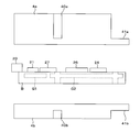
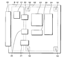
- FIG. 7 is a plan view of the circuit board B. As shown in FIGS. 6 and 7, the second conductor G2 is exposed at each of the four locations on the upper plate surface of the circuit board B. The second conductor G2 is also exposed at each of the four locations on the lower plate surface of the circuit board B. The four exposed surfaces of the second conductor G2 on the lower plate surface of the circuit board B are arranged below each of the four exposed surfaces of the second conductor G2 on the upper plate surface of the circuit board B.
- Screw holes 52 penetrating in the vertical direction are provided on each of the four exposed surfaces of the second conductor G2.
- each of the four screw 50s is inserted into the four screw holes 52 in a state where the screw portions of the four screws 50 are passed through the four through holes 42a of the upper covering body 4a from above. Tighten the four screws 50.
- the peripheral edge of the through hole 42a of the upper covering body 4a is sandwiched between the head of the screw 50 and the circuit board B.
- the peripheral edge of the through hole 42a of the upper covering body 4a comes into contact with the second conductor G2, and the upper covering body 4a conducts to the second conductor G2.
- the screw portions of the four screws 50 project to the lower side of the circuit board B.
- the screw portions of the four screw 50s protruding downward passing through the four through holes 42b of the lower covering body 4b from above, four nuts 51 are inserted into the screw portions of each of the four screw 50s. Attach from the tip.
- the peripheral edge of the through hole 42b of the lower covering body 4b is sandwiched between the nut 51 and the circuit board B.
- the peripheral edge of the through hole 42b of the lower covering body 4b comes into contact with the second conductor G2, and the lower covering body 4b conducts to the second conductor G2.
- the upper covering body 4a is conducting with the lower covering body 4b via the second conductor G2.
- the four screws 50 and the four nuts 51 are conductive and are made of, for example, metal.
- the edge of the opening surface of the upper covering body 4a is in contact with the edge of the opening surface of the lower covering body 4b.
- the upper covering body 4a is directly connected to the lower covering body 4b at the edge portion.
- the front wall of the upper covering body 4a is provided with an opening (not shown) that penetrates in the front-rear direction.
- the connector 20 is inserted through the opening of the upper covering body 4a and protrudes to the front side of the storage box 4.
- the circuit board B has a rectangular shape, and the first conductor G1 and the second conductor G2 each have a rectangular plate shape.
- the plate surfaces of the first conductor G1 and the second conductor G2 face the plate surface of the circuit board B.
- the surface area of the second conductor G2 is larger than the surface area of the first conductor G1.
- the first conductor G1 and the second conductor G2 are arranged in the front-rear direction.
- the first conductor G1 and the second conductor G2 are covered with an insulating resin in a state where they are not in contact with each other.
- the analog circuit 21 connected to the first conductor G1 and not connected to the second conductor G2 is arranged above the first conductor G1.
- the common mode choke coil 25 and the detection circuit 27 connected to both the first conductor G1 and the second conductor G2 are arranged above the first conductor G1 and the second conductor G2.
- the common mode choke coil 30 of the connection circuit 22 that is not connected to both the first conductor G1 and the second conductor G2 is also arranged above the first conductor G1 and the second conductor G2.
- the communication circuit 23, the microcomputer 24, and the regulator 26, which are not connected to the first conductor G1 and are connected to the second conductor G2, are arranged above the second conductor G2.
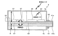
- FIG. 8 is an explanatory diagram of the effect of the storage box 4.
- the analog circuit 21, the connection circuit 22, the communication circuit 23, the microcomputer 24, the common mode choke coil 25, the regulator 26, the detection circuit 27, and the circuit board B are housed in the conductive storage box 4. Therefore, the high frequency noise generated outside the communication device 10 is difficult to enter into the communication device 10, and the high frequency noise entering the analog circuit 21, the communication circuit 23, the microcomputer 24, the detection circuit 27, and the like is small.
- high frequency noise is generated with the generation of static electricity.
- high frequency noise is generated by the interference of an electromagnetic field generated when a signal propagates through a conducting wire arranged in the vicinity of the communication device 10.
- the first conductor G1 does not conduct to the storage box 4 and the second conductor G2. Therefore, a capacitive coupling occurs between the storage box 4 and the first conductor G1, and a capacitive coupling occurs between the first conductor G1 and the second conductor G2.
- capacitive coupling occurs, stray capacitance is formed.
- the storage box 4 conducts to the second conductor G2, which has a surface area larger than the surface area of the first conductor G1. Therefore, the stray capacitance formed between the storage box 4 and the first conductor G1 having a small surface area is small, and the stray capacitance formed between the first conductor G1 and the second conductor G2 is also small.
- the high frequency noise entering the circuit connected to the second conductor G2 from the circuit connected to the first conductor G1 via the stray capacitance is small.
- High-frequency noise entering the circuit connected to the first conductor G1 from the circuit connected to the second conductor G2 via the stray capacitance is also small.
- FIG. 9 is an explanatory diagram of the analog circuit 21.
- the analog circuit 21 has a termination circuit 60 and capacitors 61 and 62.
- the termination circuit 60 is connected to the middle of the two conductors through which the differential signal propagates and to the first conductor G1.
- One end of the capacitor 61 is connected to the connector 20 and the termination circuit 60.
- the other end of the capacitor 61 is connected to one end of the first inductor 30a of the common mode choke coil 30.
- One end of the capacitor 62 is connected to the connector 20 and the termination circuit 60.
- the other end of the capacitor 62 is connected to one end of the second inductor 30b of the common mode choke coil 30.
- the termination circuit 60 executes analog processing to prevent reflection of the differential signal propagating through the two conductors.
- the reference potential of the terminal circuit 60 is the potential of the first conductor G1.
- the termination circuit 60 has resistors 70, 71, 72 and a capacitor 73. One end of each of the resistors 70 and 71 is connected to one end of the capacitors 61 and 62. The other ends of the resistors 70 and 71 are connected to one end of the capacitor 73. The other end of the capacitor 73 is connected to the first conductor G1.
- a resistor 72 is connected between both ends of the capacitor 73.
- the resistance value of the resistor 70 is a resistance value in consideration of the characteristic impedance of the propagation path of the signal propagating through the conducting wire connected to one end of the resistor 70.
- the other end of the resistor 70 is grounded via the capacitor 73. Therefore, the reflection of the signal propagating through the conducting wire connected to one end of the resistor 70 is prevented.
- the resistance value of the resistor 71 is a resistance value in consideration of the characteristic impedance of the propagation path of the signal propagating through the conducting wire connected to one end of the resistor 71.
- the other end of the resistor 71 is grounded via the capacitor 73. Therefore, the reflection of the signal propagating through the conducting wire connected to one end of the resistor 71 is prevented.
- the resistors 70 and 71 prevent reflection of the differential signal propagating through the two conductors.
- the analog processing performed by the analog circuit 21 is a processing for preventing the reflection of the differential signal, and the reference potential is the potential of the first conductor G1.
- the capacitor 73 is arranged to remove noise propagating through the two conductors. Noise propagates from the two conductors to the first conductor G1 via the capacitor 73. The capacitor 73 discharges the stored electric power through the resistor 72.
- Capacitors 61 and 62 are used for AC (Alternating Current) coupling, respectively. Each of the capacitors 61 and 62 removes the DC component from the signal input from one end via the conducting wire, and outputs the signal from which the DC component has been removed from the other end. Therefore, the capacitors 61 and 62 remove the DC component from the differential signal input via the connector 20, and also remove the DC component from the differential signal transmitted by the communication circuit 23.
- AC Alternating Current
- the communication device 10 may contain externally generated high-frequency noise.
- the reference potential is a predetermined potential, for example, the voltage of the first conductor G1, which is the potential of the ground, fluctuates at high speed.
- the current flowing through the resistors 70 and 71 cannot follow the fluctuation of the voltage of the first conductor G1. Therefore, in the two conductors on the analog circuit 21 side of the common mode choke coil 30, the voltage based on the potential of the first conductor G1 fluctuates at high speed as the voltage of the first conductor G1 fluctuates. As a result, high-frequency noise enters the analog circuit 21.
- the second inductor 25b of the common mode choke coil 25 is connected between the first conductor G1 and the second conductor G2. Therefore, even when the voltage of the first conductor G1 whose reference potential is a predetermined potential fluctuates, the voltage of the second conductor G2 whose reference potential is a predetermined potential hardly fluctuates.
- the second inductor 25b functions as a connecting element.
- the first inductor 30a of the common mode choke coil 30 is arranged in the middle of one of the conducting wires connecting the analog circuit 21 and the communication circuit 23.
- the second inductor 30b of the common mode choke coil 30 is arranged in the middle of the other conducting wire connecting the analog circuit 21 and the communication circuit 23. Therefore, even if the voltages of the two conductors fluctuate on the analog circuit 21 side of the common mode choke coil 30, the voltages of the two conductors almost fluctuate on the communication circuit 23 side of the common mode choke coil 30. There is no such thing.
- each of the common mode choke coils 25 and 30 suppresses the propagation of high frequency noise through itself.
- the high frequency noise entering the communication circuit 23 from the analog circuit 21 is small.
- the reference potential is a predetermined potential, for example, the voltage of the second conductor G2, which is the potential of the ground, fluctuates at high speed.
- the current flowing through the second conductor G2 via the communication circuit 23 cannot follow the fluctuation of the voltage of the second conductor G2. Therefore, in the two conductors on the communication circuit 23 side of the common mode choke coil 30, the voltage whose reference potential is the potential of the second conductor G2 fluctuates at high speed as the voltage of the second conductor G2 fluctuates. As a result, high frequency noise enters the communication circuit 23.
- the first conductor G1 and the second conductor G2 are connected by the second inductor 25b of the common mode choke coil 25. Therefore, even when the voltage of the second conductor G2 whose reference potential is a predetermined potential fluctuates, the voltage of the first conductor G1 whose reference potential is a predetermined potential hardly fluctuates.
- the first inductor 30a of the common mode choke coil 30 is arranged in the middle of one of the conducting wires connecting the analog circuit 21 and the communication circuit 23.
- the second inductor 30b of the common mode choke coil 30 is arranged in the middle of the other conducting wire connecting the analog circuit 21 and the communication circuit 23. Therefore, even if the voltages of the two conductors fluctuate on the communication circuit 23 side of the common mode choke coil 30, the voltages of the two conductors almost fluctuate on the analog circuit 21 side of the common mode choke coil 30. There is no such thing.
- each of the common mode choke coils 25 and 30 suppresses the propagation of high frequency noise through itself.
- the high frequency noise entering the analog circuit 21 from the communication circuit 23 is small.
- the storage box 4 is conductive with the second conductor G2. Therefore, the entry of high-frequency noise into the storage box 4 is equivalent to the entry of high-frequency noise into the second conductor G2.
- the volume of the conductor composed of the storage box 4 and the second conductor G2 is large. Therefore, the impedance of the conductor composed of the storage box 4 and the second conductor G2 is small. As a result, the fluctuation of the voltage of the second conductor G2 that occurs when the storage box 4 contains the high frequency noise or when the second conductor G2 contains the high frequency noise is small.
- FIG. 10 is an explanatory diagram of the detection circuit 27.
- the detection circuit 27 has resistors 80, 81, 82, capacitors 83, 84 and an input circuit 85.
- the input circuit 85 has an NPN type bipolar transistor 90 and a resistor 91.
- One end of the resistor 80 is connected to the connector 20, one end of the resistor 81 and the capacitor 83.
- the other ends of the resistor 81 and the capacitor 83 are connected to the first conductor G1.
- the other end of the resistor 80 is connected to the base of the bipolar transistor 90 included in the input circuit 85 and one end of the resistor 82 and the capacitor 84.
- the other ends of the resistor 82 and the capacitor 84 are connected to the second conductor G2.
- the capacitor 83 is connected to one end of the resistor 80 and between the first conductor G1.
- the capacitor 84 is connected between the other end of the resistor 80 and the second conductor G2.
- Capacitors 83 and 84 function as first and second capacitors, respectively.
- the collector of the bipolar transistor 90 is connected to one end of the resistor 91.
- a predetermined voltage Vc is applied to the other end of the resistor 91.
- the predetermined voltage Vc is a constant voltage whose reference potential is the potential of the second conductor G2.
- the predetermined voltage Vc may be, for example, a set voltage output by the regulator 26. In this case, the regulator 26 applies a predetermined voltage Vc to the other end of the resistor 91.
- the collector of the bipolar transistor 90 is further connected to the microcomputer 24.
- the emitter of the bipolar transistor 90 is connected to the second conductor G2.
- the bipolar transistor 90 functions as a switch. When the current flows in the bipolar transistor 90 in the order of the base and the emitter, the bipolar transistor 90 is switched on. When the bipolar transistor 90 is on, the resistance value between the collector and the emitter is sufficiently small, and the current flows in the order of the resistor 91 and the bipolar transistor 90. In the bipolar transistor 90, when the current flow through the base and the emitter is stopped, the bipolar transistor 90 is switched off. When the bipolar transistor 90 is off, the resistance value between the collector and the emitter is sufficiently large, and the current does not flow in the order of the resistor 91 and the bipolar transistor 90.
- the current flows in the bipolar transistor 90 in the order of the base and the emitter, and the bipolar transistor 90 is on.
- the voltage input from the connector 20 is a voltage whose reference potential is the potential of the first conductor G1.
- the voltage input from the connector 20 is less than the above-mentioned threshold voltage, the current does not flow in the bipolar transistor 90 in the order of the base and the emitter, and the bipolar transistor 90 is off.
- the diagnostic tool 12 detects a voltage whose reference potential is the potential of the first conductor G1 and which is equal to or higher than the threshold voltage 27. Output to. At this time, the current flows from the positive terminal of the diagnostic tool 12 in the order of the resistor 80, the base and emitter of the bipolar transistor 90, the second conductor G2, the second inductor 25b and the first conductor G1 to the negative terminal of the diagnostic tool 12. return. As a result, the bipolar transistor is switched on, and the current flows in the input circuit 85 in the order of the resistor 91, the bipolar transistor 90, and the second conductor G2. As a result, the input circuit 85 outputs zero V to the microcomputer 24. Zero V is a voltage whose reference potential is the potential of the second conductor G2.
- the diagnostic tool 12 when the diagnostic tool 12 is connected to the connector 20, it outputs a DC voltage to the base of the bipolar transistor 90 of the input circuit 85 via the connector 20 and the resistor 80. At this time, the input circuit 85 outputs zero V to the microcomputer 24.
- zero V is output to the detection circuit 27.
- zero V is a voltage whose reference potential is the potential of the first conductor G1 and is less than the threshold voltage.
- the current flow through the base and the emitter of the bipolar transistor 90 is stopped, and the bipolar transistor 90 is switched off.
- a predetermined voltage Vc is input to the microcomputer 24.
- a voltage equal to or higher than the threshold voltage or zero V is input to the base of the bipolar transistor 90 of the input circuit 85 via the resistor 80.
- the input circuit 85 outputs zero V to the microcomputer 24.
- the input circuit 85 outputs a predetermined voltage Vc to the microcomputer 24.
- the microcomputer 24 detects the connection of the diagnostic tool 12 to the connector 20 based on the voltage input from the input circuit 85, that is, the voltage input to the input circuit 85 via the connector 20 and the resistor 80. Specifically, the microcomputer 24 detects the connection of the diagnostic tool 12 when the voltage input to the input circuit 85 is equal to or higher than the threshold voltage.
- Each of the diagnostic tool 12 and the microcomputer 24 functions as an external device and a detection unit.
- the resistor 80 limits the magnitude of the current flowing in the order of the base and the emitter in the bipolar transistor 90. Therefore, the resistance value of the resistor 80 is relatively large.
- the resistor 81 stabilizes the voltage input from the connector 20.
- the resistor 82 stabilizes the voltage between the emitter and the base in the bipolar transistor 90.
- the capacitor 83 smoothes the voltage output from the connector 20 toward the resistor 80.
- the capacitor 84 smoothes the voltage output from the connector 20 via the resistor 80.
- the first conductor G1 and the second conductor G2 are connected by the second inductor 25b of the common mode choke coil 25. Therefore, even when the voltage of the first conductor G1 whose reference potential is a predetermined potential fluctuates, the voltage of the second conductor G2 whose reference potential is a predetermined potential hardly fluctuates.
- one end of the resistor 80 on the connector 20 side is connected to the first conductor G1 via the resistor 81.
- One end of the resistor 80 on the input circuit 85 side is connected to the second conductor G2 via the resistor 82. Therefore, even if the voltage at one end of the resistor 80 on the connector 20 side fluctuates, the voltage at one end of the resistor 80 on the input circuit 85 side hardly fluctuates.
- the voltage of the second conductor G2 whose reference potential is a predetermined potential fluctuates at high speed.
- the current flowing through the capacitor 84 cannot follow the fluctuation of the voltage of the second conductor G2. Therefore, at one end of the resistor 80 on the connector 20 side, the voltage whose reference potential is the potential of the second conductor G2 fluctuates at high speed as the voltage of the second conductor G2 fluctuates.
- the first conductor G1 and the second conductor G2 are connected by the second inductor 25b of the common mode choke coil 25. Therefore, even when the voltage of the second conductor G2 whose reference potential is a predetermined potential fluctuates, the voltage of the first conductor G1 whose reference potential is a predetermined potential hardly fluctuates.
- one end of the resistor 80 on the connector 20 side is connected to the first conductor G1 via the resistor 81.
- One end of the resistor 80 on the input circuit 85 side is connected to the second conductor G2 via the resistor 82. Therefore, even if the voltage at one end of the resistor 80 on the input circuit 85 side fluctuates, the voltage at one end of the resistor 80 on the connector 20 side hardly fluctuates.
- each of the common mode choke coil 25 and the resistor 80 suppresses the propagation of high frequency noise through itself. Therefore, when the high-frequency noise enters the first conductor G1, the high-frequency noise propagating in the order of the capacitor 83 and the resistor 80 is small, and the high-frequency noise entering the first conductor G1 to the second conductor G2 is also small. Further, when the high frequency noise enters the second conductor G2, the high frequency noise propagating in the order of the capacitor 84 and the resistor 80 is small, and the high frequency noise entering the first conductor G1 from the second conductor G2 is also small.
- FIG. 11 is an explanatory diagram of the arrangement of the resistors 80.
- the upper side of FIG. 11 shows a part of the plate surface of the circuit board B.
- the lower side of FIG. 11 shows a part of the cross section of the circuit board B.
- the resistor 80 has a rectangular parallelepiped shape, and in a plan view, the resistor 80 is arranged at the center between the first conductor G1 and the second conductor G2.
- the end faces of the first conductor G1 and the second conductor G2 face each other along the longitudinal direction of the resistor 80.
- the distance between the resistor 80 and the first conductor G1 is the same as the distance between the resistor 80 and the second conductor G2.
- "match" does not mean an exact match, but a substantial match.
- the distance between the resistor 80 and the first conductor G1 coincides with the distance between the resistor 80 and the second conductor G2.
- match does not mean an exact match, but a substantive match.
- the resistor 80 is arranged so that the distance from the first conductor G1 and the distance from the second conductor G2 match. Therefore, the distance between the first conductor G1 and the second conductor G2 is long, and the stray capacitance formed between the first conductor G1 and the second conductor G2 is even smaller.
- the second conductor G2 exposed on the upper side and the lower side of the circuit board B is in contact with the storage box 4.
- the portion of the second conductor G2 that comes into contact with the storage box 4 is not limited to the portion exposed on the upper side and the lower side of the circuit board B.
- the second embodiment will be described as different from the first embodiment.
- Other configurations except the configuration described later are common to the first embodiment. Therefore, the components common to the first embodiment are designated by the same reference numerals as those of the first embodiment, and the description thereof will be omitted.
- FIG. 12 is a plan view of the circuit board B according to the second embodiment.
- FIG. 13 is a cross-sectional view of the communication device 10 according to the second embodiment.
- the cross section shown in FIG. 13 is a cross section in the left-right direction.
- the right end surface and the left end surface of the second conductor G2 are exposed.
- the right end surface and the left end surface of the second conductor G2 are in contact with the upper covering body 4a constituting the storage box 4.
- the communication device 10 according to the second embodiment similarly exhibits the effect of the communication device 10 according to the first embodiment.
- the storage box 4 may be in contact with the second conductor G2. Therefore, the method of bringing the storage box 4 into contact with the second conductor G2 is a method of contacting the storage box 4 with the surfaces of the second conductor G2 exposed on the upper and lower sides, or the end surface of the second conductor G2. The method of contacting the storage box 4 with the container 4 is not limited to the method.
- the configuration of the storage box 4 is not limited to the configuration in which the edge of the opening surface of the upper covering body 4a contacts the edge of the opening surface of the lower covering body 4b.
- the upper covering body 4a may cover the upper side of the outer surface of the lower covering body 4b. In this case, the inner surface of the upper covering body 4a comes into contact with the outer surface of the lower covering body 4b.
- the storage box 4 is not limited to the box composed of the upper covering body 4a and the lower covering body 4b.
- the first conductor G1 and the storage box 4 may be made conductive instead of the second conductor G2.
- the communication circuit 23 transmits / receives a differential signal not only when the cable 11 is connected to the connector 20 but also when the diagnostic tool 12 is connected to the connector 20.
- the communication circuit that the diagnostic tool 12 transmits and receives when the diagnostic tool 12 is connected to the connector 20 may be a communication circuit different from the communication circuit 23.
- the communication circuit further has the same configuration as the analog circuit 21, the connection circuit 22, and the communication circuit 23.
- the communication standard of the communication performed by the diagnostic tool 12 may be different from the communication standard of the communication performed via the cable 11.
- the circuit element included in the connection circuit 22 is not limited to the common mode choke coil 30, and may be a circuit element different from the capacitor.
- two resistors may be arranged in the middle of each of the two conductors connecting the analog circuit 21 and the communication circuit 23.
- the connecting element connected between the first conductor G1 and the second conductor G2 is not limited to the second inductor 25b, and may be a circuit element different from the capacitor.
- a resistor may be connected between the first conductor G1 and the second conductor G2.
- the regulator 26 is connected to the connector 20 via an inductor. This inductor removes noise from the voltage.
- the voltage output by the diagnostic tool 12 to the input circuit 85 via the resistor 80 is not limited to the DC voltage indicating the connection, and may be the voltage related to the communication signal. That is, the diagnostic tool 12 may transmit a communication signal to the microcomputer 24 via the input circuit 85.
- the analog processing performed by the analog circuit 21 may be analog processing based on the potential of the first conductor G1. Therefore, the analog processing performed by the analog circuit 21 is not limited to the processing for preventing the reflection of the differential signal.
- the analog processing performed by the analog circuit 21 may be, for example, a processing for removing noise. In this case, for example, in the analog circuit 21, one end of two capacitors is connected in the middle of each of the two conductors through which the differential signal propagates, and the other end of the two capacitors is connected to the first conductor G1.
Landscapes
- Engineering & Computer Science (AREA)
- Computer Networks & Wireless Communication (AREA)
- Signal Processing (AREA)
- Power Engineering (AREA)
- Microelectronics & Electronic Packaging (AREA)
- Theoretical Computer Science (AREA)
- Filters And Equalizers (AREA)
- Dc Digital Transmission (AREA)
Abstract
通信装置(10)において、アナログ回路(21)は、第1導体(G1)に接続される回路素子を有し、差動信号に処理を施す。通信回路(23)は、アナログ回路(21)が処理を施した差動信号を、接続回路(22)を介して受信し、受信した差動信号に基づいて、基準電位が第2導体(G2)の電位である信号を生成する。第1導体(G1)及び第2導体(G2)間にインダクタ(25b)(接続素子)が接続されている。接続回路(22)はキャパシタを除く他の回路素子を含む。アナログ回路(21)、接続回路(22)、通信回路(23)、インダクタ(25b)、第1導体(G1)及び第2導体(G2)は、導電性の収容箱に収容されている。
Description
本開示は通信装置に関する。
本出願は、2020年3月9日出願の日本出願第2020-040059号に基づく優先権を主張し、前記日本出願に記載された全ての記載内容を援用するものである。
本出願は、2020年3月9日出願の日本出願第2020-040059号に基づく優先権を主張し、前記日本出願に記載された全ての記載内容を援用するものである。
特許文献1には、複数の通信装置が相互に通信する車両用の通信システムが開示されている。特許文献1に記載されている通信装置は、ECU(Electronic Control Unit)であり、2つの電圧の差で表される差動信号を受信する。通信装置では、差動信号がアナログ回路に入力される。アナログ回路の基準電位(ゼロVの基準)は接地電位である。アナログ回路は、入力された差動信号にアナログ処理を施す。アナログ回路がアナログ処理を施した差動信号を通信回路が受信する。通信回路は、受信した差動信号を、基準電位が接地電位であるシングルエンド信号に変換し、変換したシングルエンド信号を出力する。
本開示の一態様に係る通信装置は、第1導体及び第2導体と、前記第1導体に接続される回路素子を有し、2つの導線の電圧差で表される差動信号に処理を施すアナログ回路と、キャパシタを除く他の回路素子を含み、前記アナログ回路に接続される接続回路と、前記アナログ回路が処理を施した差動信号を、前記接続回路を介して受信し、受信した差動信号に基づいて、基準電位が前記第2導体の電位である信号を生成する通信回路と、キャパシタとは異なる回路素子であり、前記第1導体及び第2導体間に接続される接続素子と、前記第1導体、第2導体、アナログ回路、接続回路、通信回路及び接続素子が収容される導電性の収容箱とを備え、前記収容箱は、前記第1導体及び第2導体の中で表面積が大きい導体に導通している。
[本開示が解決しようとする課題]
特許文献1に記載されているような従来の通信装置においては、アナログ回路に入力した高周波ノイズが通信回路に入り、通信回路に入力した高周波ノイズがアナログ回路に入る。アナログ回路及び通信回路中の一方の回路から他方の回路に入る高周波ノイズが大きい場合、高周波ノイズが入った回路において、誤った処理が行われる可能性がある。更に、アナログ回路及び通信回路それぞれの設計において、自身の回路に入力した高周波ノイズだけではなく、他の回路から入力した高周波ノイズも考慮しなければならない。このため、アナログ回路及び通信回路それぞれの回路設計が難しいという問題がある。
特許文献1に記載されているような従来の通信装置においては、アナログ回路に入力した高周波ノイズが通信回路に入り、通信回路に入力した高周波ノイズがアナログ回路に入る。アナログ回路及び通信回路中の一方の回路から他方の回路に入る高周波ノイズが大きい場合、高周波ノイズが入った回路において、誤った処理が行われる可能性がある。更に、アナログ回路及び通信回路それぞれの設計において、自身の回路に入力した高周波ノイズだけではなく、他の回路から入力した高周波ノイズも考慮しなければならない。このため、アナログ回路及び通信回路それぞれの回路設計が難しいという問題がある。
そこで、アナログ回路及び通信回路中の一方の回路から他方の回路に入る高周波ノイズが小さい通信装置を提供することを目的とする。
[本開示の効果]
本開示によれば、アナログ回路及び通信回路中の一方の回路から他方の回路に入る高周波ノイズが小さい。
本開示によれば、アナログ回路及び通信回路中の一方の回路から他方の回路に入る高周波ノイズが小さい。
[本開示の実施形態の説明]
最初に本開示の実施態様を列挙して説明する。以下に記載する実施形態の少なくとも一部を任意に組み合わせてもよい。
最初に本開示の実施態様を列挙して説明する。以下に記載する実施形態の少なくとも一部を任意に組み合わせてもよい。
(1)本開示の一態様に係る通信装置は、第1導体及び第2導体と、前記第1導体に接続される回路素子を有し、2つの導線の電圧差で表される差動信号に処理を施すアナログ回路と、キャパシタを除く他の回路素子を含み、前記アナログ回路に接続される接続回路と、前記アナログ回路が処理を施した差動信号を、前記接続回路を介して受信し、受信した差動信号に基づいて、基準電位が前記第2導体の電位である信号を生成する通信回路と、キャパシタとは異なる回路素子であり、前記第1導体及び第2導体間に接続される接続素子と、前記第1導体、第2導体、アナログ回路、接続回路、通信回路及び接続素子が収容される導電性の収容箱とを備え、前記収容箱は、前記第1導体及び第2導体の中で表面積が大きい導体に導通している。
上記の態様にあっては、キャパシタを除く他の回路素子、例えば、インダクタ又は抵抗等を含む接続回路を介して、アナログ回路は、アナログ処理を施した差動信号を通信回路に送信する。第1導体及び第2導体間に、インダクタ又は抵抗等の接続素子が接続されている。接続回路及び接続素子それぞれは、自身を介した高周波ノイズの伝播を抑制する。このため、高周波ノイズがアナログ回路に入った場合において、アナログ回路から通信回路に入る高周波ノイズは小さい。同様に、高周波ノイズが通信回路に入った場合において、通信回路からアナログ回路に入る高周波ノイズは小さい。
また、第1導体、第2導体、アナログ回路、接続回路、通信回路及び接続素子が収容箱に収容されているので、アナログ回路及び通信回路に入る高周波ノイズは小さい。更に、アナログ回路及び通信回路から外部に出る高周波ノイズも小さい。更に、第1導体及び第2導体の中で表面積が大きい一方の導体に収容箱は導通している。このため、収容箱と他方の導体との間に形成される浮遊容量と、第1導体及び第2導体間に形成される浮遊容量とは小さい。結果、浮遊容量を介してアナログ回路から通信回路に入る高周波ノイズは小さく、浮遊容量を介して通信回路からアナログ回路に入る高周波ノイズも小さい。
(2)本開示の一態様に係る通信装置では、前記第2導体の表面積は前記第1導体の表面積よりも大きい。
上記の態様にあっては、アナログ回路に接続されている第1導体の表面積は小さく、通信回路に接続されている第2導体の表面積は大きい。
(3)本開示の一態様に係る通信装置は、抵抗と、前記抵抗を介して、電圧が入力される入力回路と、前記抵抗の一端及び前記第1導体間に接続される第1キャパシタと、前記抵抗の他端及び前記第2導体間に接続される第2キャパシタとを備える。
上記の態様にあっては、抵抗及び接続素子それぞれは、自身を介した高周波ノイズの伝播を抑制する。このため、高周波ノイズが第1導体に入った場合において、第1キャパシタ及び抵抗の順に伝播する高周波ノイズは小さく、第1導体から第2導体に入る高周波ノイズも小さい。高周波ノイズが第2導体に入った場合において、第2キャパシタ及び抵抗の順に伝播する高周波ノイズは小さく、第2導体から第1導体に入る高周波ノイズも小さい。
(4)本開示の一態様に係る通信装置は、外部装置に着脱可能に接続されるコネクタと、前記入力回路に入力された電圧に基づいて前記コネクタへの前記外部装置の接続を検知する検知部とを備え、前記コネクタ及び抵抗を介して電圧が前記入力回路に入力され、前記検知部は、前記入力回路に入力された電圧が閾値電圧以上である場合に前記外部装置の接続を検知する。
上記の態様にあっては、コネクタ及び抵抗を介して入力回路に入力された電圧が閾値電圧以上である場合にコネクタへの外部装置の接続を検知する。
(5)本開示の一態様に係る通信装置では、前記抵抗及び第1導体間の距離は、前記抵抗及び第2導体間の距離と一致している。
上記の態様にあっては、第1導体との距離と、第2導体との距離とが一致するように抵抗が配置される。このため、第1導体及び第2導体間の距離が長く、第1導体及び第2導体間に形成される浮遊容量は更に小さい。
(6)本開示の一態様に係る通信装置では、前記アナログ回路は、差動信号の反射を防止する終端回路を有し、前記終端回路は、差動信号が伝播する2つの導線の中途と、前記第1導体とに接続している。
上記の態様にあっては、差動信号が伝播する2つの導線の中途と、第1導体とに終端回路が接続している。終端回路は、差動信号の反射を防止する。
(7)本開示の一態様に係る通信装置では、前記接続回路は、コモンモードチョークコイルを有し、前記通信回路は、前記接続回路を介して差動信号を送信する。
上記の態様にあっては、接続回路はコモンモードチョークコイルを有する。コモンモードチョークコイルは2つのインダクタを有する。2つのインダクタそれぞれは、アナログ回路及び通信回路を接続する2つの導線の中途に配置されている。差動信号は、2つの導線を介して伝播する。コモンモードチョークコイルは、アナログ回路から通信回路へ伝播する差動信号からコモンモードノイズを除去するとともに、通信回路からアナログ回路へ伝播する差動信号からコモンモードノイズを除去する。
(8)本開示の一態様に係る通信装置は、基準電位が前記第1導体の電位である直流の電圧からノイズを除去する除去器を備え、前記除去器は、基準電位が前記第2導体の電位であってノイズが除去された電圧を、電力供給のための電力線に印加し、前記除去器はインダクタを有し、前記インダクタは前記接続素子である。
上記の態様にあっては、除去器は、基準電位が第1導体の電位である電圧からノイズを除去し、基準電位が第2導体の電位であってノイズが除去された電圧を電力線に印加する。除去器は、例えば、コモンモードチョークコイルであり、インダクタを有する。このインダクタが接続素子として第1導体及び第2導体間に接続されている。
[本開示の実施形態の詳細]
本開示の実施形態に係る通信装置の具体例を、以下に図面を参照しつつ説明する。なお、本発明はこれらの例示に限定されるものではなく、請求の範囲によって示され、請求の範囲と均等の意味および範囲内でのすべての変更が含まれることが意図される。
本開示の実施形態に係る通信装置の具体例を、以下に図面を参照しつつ説明する。なお、本発明はこれらの例示に限定されるものではなく、請求の範囲によって示され、請求の範囲と均等の意味および範囲内でのすべての変更が含まれることが意図される。
<通信装置の概要>
図1は、本実施形態における通信装置10の概要の説明図である。通信装置10は、ECU(Electronic Control Unit)又はゲートウェイ等であり、車両に搭載される。通信装置10はコネクタ20を備える。コネクタ20は、ケーブル11、又は、ダイアグツール12のコネクタ12aに着脱可能に接続される。
図1は、本実施形態における通信装置10の概要の説明図である。通信装置10は、ECU(Electronic Control Unit)又はゲートウェイ等であり、車両に搭載される。通信装置10はコネクタ20を備える。コネクタ20は、ケーブル11、又は、ダイアグツール12のコネクタ12aに着脱可能に接続される。
ケーブル11が通信装置10のコネクタ20に接続している場合、電力がケーブル11を介して通信装置10に供給され、通信装置10が作動する。通信装置10は、ケーブル11を介して、図示しない他の通信装置と差動信号の送受信を行う。通信装置10は、Broad-Reachと呼ばれる通信規格、又は、CAN(Controller Area Network)の通信規格等に基づく送受信を行う。
通信装置10が、例えば、車両のドアの施錠及び解錠を行うモータの動作を制御するECUである場合においては、通信装置10は、ドアの解錠を指示する差動信号を受信したとき、モータにドアを解錠させる。例えば、車両のドアが施錠されているか否かを検知するセンサが通信装置10に接続されている場合においては、通信装置10は、センサの検知結果を示す差動信号を他の通信装置に送信し、検知結果を通知する。
ダイアグツール12のコネクタ12aが通信装置10のコネクタ20に接続している場合、ダイアグツール12は通信装置10に電力を供給する。これにより、通信装置10は作動する。通信装置10及びダイアグツール12は相互に通信する。例えば、通信装置10は、故障の検知に用いるデータ、所謂ログデータを含む差動信号をダイアグツール12に送信する。また、例えば、ダイアグツール12は、通信装置10で実行されるコンピュータプログラムを更新するための更新データを含む差動信号を通信装置10に送信する。
<通信装置10の構成>
図2は、通信装置10の要部構成を示すブロック図である。通信装置10は、コネクタ20に加えて、アナログ回路21、接続回路22、通信回路23、マイクロコンピュータ(以下、マイコンという)24、コモンモードチョークコイル25、レギュレータ26、検知回路27、第1導体G1及び第2導体G2を備える。これらは、導線によって接続される。電力供給に用いられる導線、即ち、電力線を太い実線で示している。第1導体G1及び第2導体G2それぞれは、導電性を有し、例えば、金属製である。
図2は、通信装置10の要部構成を示すブロック図である。通信装置10は、コネクタ20に加えて、アナログ回路21、接続回路22、通信回路23、マイクロコンピュータ(以下、マイコンという)24、コモンモードチョークコイル25、レギュレータ26、検知回路27、第1導体G1及び第2導体G2を備える。これらは、導線によって接続される。電力供給に用いられる導線、即ち、電力線を太い実線で示している。第1導体G1及び第2導体G2それぞれは、導電性を有し、例えば、金属製である。
接続回路22はコモンモードチョークコイル30を有する。コモンモードチョークコイル30は、第1インダクタ30a及び第2インダクタ30bを有する。コモンモードチョークコイル30では、図示しない環状の磁性体に第1インダクタ30a及び第2インダクタ30bが巻き付いている。コモンモードチョークコイル25は、第1インダクタ25a及び第2インダクタ25bを有する。コモンモードチョークコイル25は、コモンモードチョークコイル30と同様に構成されている。
コネクタ20は、アナログ回路21に2つの導線によって接続されている。アナログ回路21には、更に、コモンモードチョークコイル30の第1インダクタ30a及び第2インダクタ30bの一端が2つの導線によって接続されている。アナログ回路21は、更に、導線によって第1導体G1に接続されている。第1導体G1への接続は、所謂接地である。コモンモードチョークコイル30の第1インダクタ30a及び第2インダクタ30bの他端は通信回路23に2つの導線によって接続されている。通信回路23は、更に、2つの導線によって、マイコン24及び第2導体G2に接続されている。第2導体G2への接続も所謂接地である。
コネクタ20は、更に、導線によって、コモンモードチョークコイル25の第1インダクタ25aの一端に接続されている。コネクタ20は、更に、導線によって、コモンモードチョークコイル25の第2インダクタ25bの一端と、第1導体G1とに接続されている。第1インダクタ25aの他端は、導線によってレギュレータ26に接続されている。第2インダクタ25bの他端は、導線によって第2導体G2に接続されている。レギュレータ26は、更に、2つの導線によって、マイコン24及び第2導体G2に接続されている。マイコン24は、更に、導線によって第2導体G2に接続されている。
コネクタ20は、更に、2つの導線によって検知回路27及び第1導体G1に接続されている。検知回路27は、更に、3つの導線によって、マイコン24、第1導体G1及び第2導体G2に接続されている。
ケーブル11がコネクタ20に接続された場合、ケーブル11は、アナログ回路21、コモンモードチョークコイル25及び第1導体G1に接続される。コネクタ20及び検知回路27を接続する導線において、コネクタ20側の一端は開放される。
ダイアグツール12のコネクタ12aがコネクタ20に接続された場合、ダイアグツール12のコネクタ12aは、アナログ回路21、コモンモードチョークコイル25、検知回路27及び第1導体G1に接続される。
ダイアグツール12のコネクタ12aがコネクタ20に接続された場合、ダイアグツール12のコネクタ12aは、アナログ回路21、コモンモードチョークコイル25、検知回路27及び第1導体G1に接続される。
差動信号は、ケーブル11又はダイアグツール12から、コネクタ20を介してアナログ回路21に入力される。差動信号は、2値信号であり、2つの導線の電圧差で表される。例えば、所定値以上の電圧差によって差動信号の「0」が表され、所定値未満の電圧差によって差動信号の「1」が表される。差動信号は2つの導線を介して伝播する。
アナログ回路21の基準電位(ゼロVの基準)は第1導体G1の電位である。アナログ回路21は、コネクタ20から入力された差動信号にアナログ処理を施す。通信回路23は、アナログ回路21がアナログ処理を施した差動信号を、接続回路22のコモンモードチョークコイル30を介して受信する。
アナログ回路21の基準電位(ゼロVの基準)は第1導体G1の電位である。アナログ回路21は、コネクタ20から入力された差動信号にアナログ処理を施す。通信回路23は、アナログ回路21がアナログ処理を施した差動信号を、接続回路22のコモンモードチョークコイル30を介して受信する。
コモンモードチョークコイル30は、アナログ回路21がアナログ処理を施した差動信号からコモンモードノイズを除去し、コモンモードノイズを除去した差動信号を通信回路23に出力する。コモンモードノイズは、差動信号が伝播する2つの導線に同相で重畳するノイズである。接続回路22はキャパシタを除く他の回路素子を含む。
通信回路23は、受信した差動信号に基づいて、基準電位が第2導体G2の電位であるシングルエンド信号を生成し、生成したシングルエンド信号をマイコン24に出力する。マイコン24は、通信回路23から入力されたシングルエンド信号の電圧を読み取る。これにより、マイコン24は、シングルエンド信号に含まれるデータを取得する。マイコン24は、通信回路23から入力されたシングルエンド信号に含まれるデータに基づいて種々の処理を実行する。
マイコン24は、基準電位が第2導体G2の電位であるシングルエンド信号を通信回路23に出力する。通信回路23は、マイコン24から入力されたシングルエンド信号に基づいて差動信号に生成する。通信回路23は、生成した差動信号を、接続回路22、アナログ回路21及びコネクタ20を介して、図示しない通信装置又はダイアグツール12に送信する。接続回路22のコモンモードチョークコイル30は、通信回路23が送信した差動信号からコモンモードノイズを除去する。コモンモードチョークコイル30は、コモンモードノイズを除去した差動信号を、アナログ回路21及びコネクタ20を介して出力する。
ケーブル11又はダイアグツール12から、コネクタ20を介して、コモンモードチョークコイル25に、基準電位が第1導体G1の電位である直流の電圧が入力される。コモンモードチョークコイル25は、第1インダクタ25a及び第2インダクタ25bに入力した電圧からコモンモードノイズを除去する。コモンモードチョークコイル25がコモンモードノイズを除去した電圧は、基準電位が第2導体G2の電位である電圧である。コモンモードチョークコイル25は、コモンモードノイズを除去した電圧を、レギュレータ26に接続されている導線に印加する。これにより、コモンモードノイズを除去した電圧がレギュレータ26に出力される。コモンモードチョークコイル25は除去器として機能する。図2に示すように、コネクタ20及び第1インダクタ25a間に接続される導線と、第1インダクタ25a及びレギュレータ26間に接続される導線と、レギュレータ26及びマイコン24間に接続される導線とは電力線である。
レギュレータ26は、コモンモードチョークコイル25から入力された直流の電圧を、予め設定されている設定電圧に変換する。設定電圧は、基準電位が第2導体G2の電位である直流の電圧である。レギュレータ26は、変換した設定電圧をマイコン24に出力する。これにより、マイコン24に電力が供給される。
なお、レギュレータ26は、更に、通信回路23に設定電圧を出力し、通信回路23に電力を供給してもよい。
なお、レギュレータ26は、更に、通信回路23に設定電圧を出力し、通信回路23に電力を供給してもよい。
ダイアグツール12のコネクタ12aがコネクタ20に接続された場合、ダイアグツール12は、基準電位が第1導体G1の電位である直流の電圧を検知回路27に出力し続ける。ダイアグツール12が出力する電圧は、予め設定されている閾値電圧以上である。ダイアグツール12のコネクタ12aがコネクタ20に接続されていない場合、ゼロVが検知回路27に出力される。ここで、ゼロVは、基準電位が第1導体G1の電位である電圧であり、閾値電圧未満である。
検知回路27は、第2導体G2の電位を基準とした電圧をマイコン24に出力する。検知回路27は、ゼロV又は所定電圧Vc(図10参照)を出力する。検知回路27は、コネクタ20から入力された電圧が閾値電圧以上である場合、即ち、ダイアグツール12が接続されている場合、ゼロVをマイコン24に出力する。検知回路27は、コネクタ20から入力された電圧が閾値電圧未満である場合、即ち、ダイアグツール12が接続されていない場合、所定電圧Vcをマイコン24に出力する。マイコン24は、検知回路27から入力された電圧に基づいて、コネクタ20へのダイアグツール12のコネクタ12aの接続を検知する。
<通信装置10の外観>
図3は通信装置10の分解図である。回路基板Bの上側の板面に、コネクタ20、アナログ回路21、接続回路22、通信回路23、マイコン24、コモンモードチョークコイル25、レギュレータ26及び検知回路27が配置されている。図3では、コネクタ20、アナログ回路21、マイコン24、レギュレータ26及び検知回路27が示されている。回路基板B内に、第1導体G1及び第2導体G2が配置されている。コネクタ20は、回路基板Bの前側の前縁部に配置されている。コネクタ20の一部は前縁よりも前側に突出している。
図3は通信装置10の分解図である。回路基板Bの上側の板面に、コネクタ20、アナログ回路21、接続回路22、通信回路23、マイコン24、コモンモードチョークコイル25、レギュレータ26及び検知回路27が配置されている。図3では、コネクタ20、アナログ回路21、マイコン24、レギュレータ26及び検知回路27が示されている。回路基板B内に、第1導体G1及び第2導体G2が配置されている。コネクタ20は、回路基板Bの前側の前縁部に配置されている。コネクタ20の一部は前縁よりも前側に突出している。
回路基板Bの上側の板面には、図示しないスルーホール及び導電路が設けられている。導電路は、所謂回路パターンである。スルーホール及び導電路を用いて、第1導体G1又は第2導体G2への接続が実現される。具体的には、スルーホールの面に導箔が貼り付けられている。導箔は導電路と導通している。導箔及び導電路の両方、又は、導電路によって、導線が形成されている。
図4は通信装置10の平面図である。図5は通信装置10の側面図である。図6は通信装置10の断面図である。図3~図6に示すように、通信装置10では、アナログ回路21、接続回路22、通信回路23、マイコン24、コモンモードチョークコイル25、レギュレータ26、検知回路27及び回路基板Bは、導電性の収容箱4に収容されている。収容箱4は例えば金属製である。
収容箱4は、回路基板Bの上側の板面を覆う導電性の上側覆い体4aと、回路基板Bの下側の板面を覆う導電性の下側覆い体4bとによって構成される。上側覆い体4a及び下側覆い体4bそれぞれは、一面が開放された箱体状をなす。上側覆い体4aは、底壁が上側となるように配置されている。下側覆い体4bは、底壁が下側となるように配置されている。上側覆い体4aの開口面の縁部は、下側覆い体4bの開口面の縁部と接触している。上側覆い体4aの内部に回路基板Bの上側の板面が配置される。下側覆い体4bの内部に回路基板Bの下側の板面が配置される。
上側覆い体4aの底壁には、下側に凹んだ凹部40a,41aが形成されている。上側覆い体4aの底壁は、矩形状をなし、回路基板Bの上側の板面と対向している。2つの凹部40aそれぞれは、上側覆い体4aの底面の左辺部及び右辺部の中途に設けられている。上側覆い体4aの底壁の後辺部全体が凹んでおり、これにより、凹部41aが形成されている。
下側覆い体4bの底壁には、上側に凹んだ凹部40b,41bが形成されている。下側覆い体4bの底壁は、矩形状をなし、回路基板Bの下側の板面と対向している。2つの凹部40aそれぞれは、下側覆い体4bの底壁の左辺部及び右辺部の中途に設けられている。下側覆い体4bの底壁の後辺部全体が凹んでおり、これにより、凹部41bが形成されている。図6に示すように、上側覆い体4aの凹部40a,41aそれぞれの底面は、下側覆い体4bの凹部40b,41bの底面に対向している。
上側覆い体4aには、上下方向に貫通する4つの貫通孔42aが設けられている。図4に示すように、2つの貫通孔42aそれぞれは、2つの凹部40aの底壁に設けられている。残り2つの貫通孔42aそれぞれは、凹部41aの左側及び右側に設けられている。同様に、下側覆い体4bにも、上下方向に貫通する4つの貫通孔42bが設けられている。2つの貫通孔42bそれぞれは、2つの凹部40bの底壁に設けられている。残り2つの貫通孔42bそれぞれは、凹部41bの左側及び右側に設けられている。上側覆い体4aの4つの貫通孔42aそれぞれは、下側覆い体4bの4つの貫通孔42bに対向している。
図7は回路基板Bの平面図である。図6及び図7に示すように、回路基板Bの上側の板面の4箇所それぞれにおいて、第2導体G2は露出している。回路基板Bの下側の板面の4箇所それぞれにおいても、第2導体G2は露出している。回路基板Bの上側の板面における第2導体G2の4つの露出面それぞれの下側に、回路基板Bの下側の板面における第2導体G2の4つの露出面が配置されている。
第2導体G2の4つの露出面それぞれにおいて、上下方向に貫通する螺子孔52が設けられている。図6に示すように、上側覆い体4aの4つの貫通孔42aそれぞれに4つの螺子50の螺子部を上側から通している状態で、4つの螺子50それぞれを4つの螺子孔52に挿入する。4つの螺子50を締める。これにより、上側覆い体4aの貫通孔42aの周縁部は、螺子50の頭部と回路基板Bとによって挟まれる。このとき、上側覆い体4aの貫通孔42aの周縁部は第2導体G2に接触し、上側覆い体4aは第2導体G2に導通する。
4つの螺子50を締めた場合、4つの螺子50の螺子部は回路基板Bの下側に突出している。下側覆い体4bの4つの貫通孔42bそれぞれに、下側に突出している4つの螺子50の螺子部を上側から通している状態で、4つの螺子50それぞれの螺子部に4つのナット51を先端から装着する。これにより、下側覆い体4bの貫通孔42bの周縁部は、ナット51と回路基板Bとによって挟まれる。このとき、下側覆い体4bの貫通孔42bの周縁部は第2導体G2に接触し、下側覆い体4bは第2導体G2に導通する。上側覆い体4aは、第2導体G2を介して下側覆い体4bと導通している。4つの螺子50及び4つのナット51は、導電性を有し、例えば金属製である。
前述したように、上側覆い体4aの開口面の縁部は、下側覆い体4bの開口面の縁部と接触している。上側覆い体4aは、縁部分において下側覆い体4bと直接に導通している。上側覆い体4aの前壁には、前後方向に貫通する図示しない開口が設けられている。コネクタ20は、上側覆い体4aの開口を挿通し、収容箱4の前側に突出している。
<通信装置10の構成部の配置>
図3及び図7に示すように、回路基板Bは矩形状をなし、第1導体G1及び第2導体G2それぞれは矩形板状をなす。第1導体G1及び第2導体G2の板面は、回路基板Bの板面と対向している。第2導体G2の表面積は、第1導体G1の表面積よりも大きい。第1導体G1及び第2導体G2は、前後方向に並べられている。第1導体G1及び第2導体G2は、互いに接触していない状態で、絶縁性の樹脂によって覆われている。
図3及び図7に示すように、回路基板Bは矩形状をなし、第1導体G1及び第2導体G2それぞれは矩形板状をなす。第1導体G1及び第2導体G2の板面は、回路基板Bの板面と対向している。第2導体G2の表面積は、第1導体G1の表面積よりも大きい。第1導体G1及び第2導体G2は、前後方向に並べられている。第1導体G1及び第2導体G2は、互いに接触していない状態で、絶縁性の樹脂によって覆われている。
図7に示すように、第1導体G1に接続し、かつ、第2導体G2に接続しないアナログ回路21は、第1導体G1の上側に配置されている。第1導体G1及び第2導体G2の両方に接続するコモンモードチョークコイル25及び検知回路27は、第1導体G1及び第2導体G2の上側に配置されている。第1導体G1及び第2導体G2の両方に接続しない接続回路22のコモンモードチョークコイル30も、第1導体G1及び第2導体G2の上側に配置されている。第1導体G1に接続せず、かつ、第2導体G2に接続する通信回路23、マイコン24及びレギュレータ26は、第2導体G2の上側に配置されている。
図8は収容箱4の効果の説明図である。前述したように、アナログ回路21、接続回路22、通信回路23、マイコン24、コモンモードチョークコイル25、レギュレータ26、検知回路27及び回路基板Bは、導電性の収容箱4に収容されている。このため、通信装置10の外部で発生した高周波ノイズは通信装置10内に入りにくく、アナログ回路21、通信回路23、マイコン24及び検知回路27等に入る高周波ノイズは小さい。一例として、高周波ノイズは、静電気の発生に伴って発生する。他例として、高周波ノイズは、通信装置10の近傍に配置された導線を信号が伝播した場合に発生する電磁界の干渉によって発生する。
また、アナログ回路21、通信回路23、マイコン24及び検知回路27等で発生した高周波ノイズは、通信装置10の外部に出にくい。結果、アナログ回路21、通信回路23、マイコン24及び検知回路27等から通信装置10の外部に出る高周波ノイズも小さい。
第1導体G1は、収容箱4及び第2導体G2に導通していない。従って、収容箱4及び第1導体G1間において容量結合は発生し、第1導体G1及び第2導体G2間において容量結合が発生する。容量結合が発生した場合、浮遊容量が形成される。
通信装置10では、収容箱4は、第1導体G1の表面積よりも表面積が大きい第2導体G2に導通している。このため、収容箱4と表面積が小さい第1導体G1との間に形成される浮遊容量は小さく、第1導体G1及び第2導体G2間に形成される浮遊容量も小さい。従って、浮遊容量を介して、第1導体G1に接続している回路から、第2導体G2に接続している回路に入る高周波ノイズは小さい。浮遊容量を介して、第2導体G2に接続している回路から、第1導体G1に接続している回路に入る高周波ノイズも小さい。
通信装置10では、収容箱4は、第1導体G1の表面積よりも表面積が大きい第2導体G2に導通している。このため、収容箱4と表面積が小さい第1導体G1との間に形成される浮遊容量は小さく、第1導体G1及び第2導体G2間に形成される浮遊容量も小さい。従って、浮遊容量を介して、第1導体G1に接続している回路から、第2導体G2に接続している回路に入る高周波ノイズは小さい。浮遊容量を介して、第2導体G2に接続している回路から、第1導体G1に接続している回路に入る高周波ノイズも小さい。
<アナログ回路21の構成>
図9はアナログ回路21の説明図である。アナログ回路21は、終端回路60及びキャパシタ61,62を有する。終端回路60は、差動信号が伝播する2つの導線の中途と、第1導体G1とに接続されている。キャパシタ61の一端は、コネクタ20及び終端回路60に接続されている。キャパシタ61の他端は、コモンモードチョークコイル30の第1インダクタ30aの一端に接続されている。キャパシタ62の一端は、コネクタ20及び終端回路60に接続されている。キャパシタ62の他端は、コモンモードチョークコイル30の第2インダクタ30bの一端に接続されている。
図9はアナログ回路21の説明図である。アナログ回路21は、終端回路60及びキャパシタ61,62を有する。終端回路60は、差動信号が伝播する2つの導線の中途と、第1導体G1とに接続されている。キャパシタ61の一端は、コネクタ20及び終端回路60に接続されている。キャパシタ61の他端は、コモンモードチョークコイル30の第1インダクタ30aの一端に接続されている。キャパシタ62の一端は、コネクタ20及び終端回路60に接続されている。キャパシタ62の他端は、コモンモードチョークコイル30の第2インダクタ30bの一端に接続されている。
終端回路60は、2つの導線を介して伝播する差動信号の反射を防止するアナログ処理を実行する。終端回路60の基準電位は、第1導体G1の電位である。終端回路60は、抵抗70,71,72及びキャパシタ73を有する。抵抗70,71それぞれの一端は、キャパシタ61,62の一端に接続されている。抵抗70,71それぞれの他端は、キャパシタ73の一端に接続されている。キャパシタ73の他端は第1導体G1に接続されている。キャパシタ73の両端間には、抵抗72が接続されている。
抵抗70の抵抗値は、抵抗70の一端に接続されている導線を伝播する信号の伝播路の特性インピーダンスを考慮した抵抗値である。抵抗70の他端は、キャパシタ73を介して接地されている。このため、抵抗70の一端に接続されている導線を伝播する信号の反射が防止される。同様に、抵抗71の抵抗値は、抵抗71の一端に接続されている導線を伝播する信号の伝播路の特性インピーダンスを考慮した抵抗値である。抵抗71の他端は、キャパシタ73を介して接地されている。このため、抵抗71の一端に接続されている導線を伝播する信号の反射が防止される。結果、抵抗70,71は、2つの導線を伝播する差動信号の反射を防止する。
以上のように、アナログ回路21が行うアナログ処理は、差動信号の反射を防止する処理であり、基準電位が第1導体G1の電位である処理である。
以上のように、アナログ回路21が行うアナログ処理は、差動信号の反射を防止する処理であり、基準電位が第1導体G1の電位である処理である。
キャパシタ73は、2つの導線を伝播したノイズを除去するために配置される。ノイズは、2つの導線からキャパシタ73を介して第1導体G1に伝播する。キャパシタ73は、蓄えた電力を、抵抗72を介して放出する。
キャパシタ61,62それぞれは、AC(Alternating Current)結合のために用いられる。キャパシタ61,62それぞれは、導線を介して、一端から入力された信号から直流成分を除去し、直流成分を除去した信号を他端から出力する。従って、キャパシタ61,62は、コネクタ20を介して入力された差動信号から直流成分を除去するとともに、通信回路23が送信した差動信号から直流成分を除去する。
<コモンモードチョークコイル25,30の効果>
前述したように、通信装置10には、外部で発生した高周波ノイズが入る可能性がある。第1導体G1に高周波ノイズが入った場合、基準電位が所定電位、例えば、地面の電位である第1導体G1の電圧が高速に変動する。抵抗70,71を介して流れる電流は、第1導体G1の電圧の変動に追随することができない。このため、コモンモードチョークコイル30のアナログ回路21側の2つの導線では、第1導体G1の電圧の変動に伴って、第1導体G1の電位を基準とした電圧が高速に変動する。これにより、アナログ回路21に高周波ノイズが入る。
前述したように、通信装置10には、外部で発生した高周波ノイズが入る可能性がある。第1導体G1に高周波ノイズが入った場合、基準電位が所定電位、例えば、地面の電位である第1導体G1の電圧が高速に変動する。抵抗70,71を介して流れる電流は、第1導体G1の電圧の変動に追随することができない。このため、コモンモードチョークコイル30のアナログ回路21側の2つの導線では、第1導体G1の電圧の変動に伴って、第1導体G1の電位を基準とした電圧が高速に変動する。これにより、アナログ回路21に高周波ノイズが入る。
第1導体G1及び第2導体G2間に、コモンモードチョークコイル25の第2インダクタ25bが接続されている。このため、基準電位が所定電位である第1導体G1の電圧が変動した場合であっても、基準電位が所定電位である第2導体G2の電圧は殆ど変動しない。第2インダクタ25bは接続素子として機能する。
また、アナログ回路21及び通信回路23間を接続する一方の導線の中途に、コモンモードチョークコイル30の第1インダクタ30aが配置されている。アナログ回路21及び通信回路23間を接続する他方の導線の中途に、コモンモードチョークコイル30の第2インダクタ30bが配置されている。このため、コモンモードチョークコイル30のアナログ回路21側において、2つの導線の電圧が変動した場合であっても、コモンモードチョークコイル30の通信回路23側において、2つの導線の電圧は殆ど変動することはない。
以上のように、コモンモードチョークコイル25,30それぞれは、自身を介した高周波ノイズの伝播を抑制する。アナログ回路21から通信回路23に入る高周波ノイズは小さい。
第2導体G2に高周波ノイズが入った場合、基準電位が所定電位、例えば、地面の電位である第2導体G2の電圧が高速に変動する。通信回路23を介して第2導体G2に流れる電流は、第2導体G2の電圧の変動に追随することができない。このため、コモンモードチョークコイル30の通信回路23側の2つの導線では、第2導体G2の電圧の変動に伴って、基準電位が第2導体G2の電位である電圧が高速に変動する。これにより、高周波ノイズが通信回路23に入る。
前述したように、第1導体G1及び第2導体G2は、コモンモードチョークコイル25の第2インダクタ25bによって接続されている。このため、基準電位が所定電位である第2導体G2の電圧が変動した場合であっても、基準電位が所定電位である第1導体G1の電圧は殆ど変動しない。
また、アナログ回路21及び通信回路23間を接続する一方の導線の中途に、コモンモードチョークコイル30の第1インダクタ30aが配置されている。アナログ回路21及び通信回路23間を接続する他方の導線の中途に、コモンモードチョークコイル30の第2インダクタ30bが配置されている。このため、コモンモードチョークコイル30の通信回路23側において、2つの導線の電圧が変動した場合であっても、コモンモードチョークコイル30のアナログ回路21側において、2つの導線の電圧は殆ど変動することはない。
以上のように、コモンモードチョークコイル25,30それぞれは、自身を介した高周波ノイズの伝播を抑制する。通信回路23からアナログ回路21に入る高周波ノイズは小さい。
なお、前述したように、収容箱4は第2導体G2と導通している。このため、収容箱4に高周波ノイズが入ることは、第2導体G2に高周波ノイズが入ることと等価である。しかしながら、収容箱4及び第2導体G2によって構成される導体の体積は大きい。このため、収容箱4及び第2導体G2によって構成される導体のインピーダンスは小さい。結果、収容箱4に高周波ノイズが入った場合、又は、第2導体G2に高周波ノイズが入った場合に生じる第2導体G2の電圧の変動は小さい。
なお、前述したように、収容箱4は第2導体G2と導通している。このため、収容箱4に高周波ノイズが入ることは、第2導体G2に高周波ノイズが入ることと等価である。しかしながら、収容箱4及び第2導体G2によって構成される導体の体積は大きい。このため、収容箱4及び第2導体G2によって構成される導体のインピーダンスは小さい。結果、収容箱4に高周波ノイズが入った場合、又は、第2導体G2に高周波ノイズが入った場合に生じる第2導体G2の電圧の変動は小さい。
<検知回路27の構成>
図10は検知回路27の説明図である。検知回路27は、抵抗80,81,82、キャパシタ83,84及び入力回路85を有する。入力回路85は、NPN型のバイポーラトランジスタ90及び抵抗91を有する。抵抗80の一端は、コネクタ20と、抵抗81及びキャパシタ83の一端とに接続されている。抵抗81及びキャパシタ83の他端は第1導体G1に接続されている。抵抗80の他端は、入力回路85が有するバイポーラトランジスタ90のベースと、抵抗82及びキャパシタ84の一端とに接続されている。抵抗82及びキャパシタ84の他端は第2導体G2に接続されている。
図10は検知回路27の説明図である。検知回路27は、抵抗80,81,82、キャパシタ83,84及び入力回路85を有する。入力回路85は、NPN型のバイポーラトランジスタ90及び抵抗91を有する。抵抗80の一端は、コネクタ20と、抵抗81及びキャパシタ83の一端とに接続されている。抵抗81及びキャパシタ83の他端は第1導体G1に接続されている。抵抗80の他端は、入力回路85が有するバイポーラトランジスタ90のベースと、抵抗82及びキャパシタ84の一端とに接続されている。抵抗82及びキャパシタ84の他端は第2導体G2に接続されている。
以上のように、キャパシタ83は抵抗80の一端及び第1導体G1間に接続されている。キャパシタ84は、抵抗80の他端及び第2導体G2間に接続されている。キャパシタ83,84それぞれは、第1キャパシタ及び第2キャパシタとして機能する。
入力回路85では、バイポーラトランジスタ90のコレクタは、抵抗91の一端に接続されている。抵抗91の他端には、所定電圧Vcが印加されている。所定電圧Vcは、基準電位が第2導体G2の電位である一定の電圧である。所定電圧Vcは、例えば、レギュレータ26が出力する設定電圧であってもよい。この場合、レギュレータ26が所定電圧Vcを抵抗91の他端に印加する。バイポーラトランジスタ90のコレクタは、更に、マイコン24に接続されている。バイポーラトランジスタ90のエミッタは第2導体G2に接続されている。
バイポーラトランジスタ90はスイッチとして機能する。バイポーラトランジスタ90において電流がベース及びエミッタの順に流れた場合、バイポーラトランジスタ90はオンに切替わる。バイポーラトランジスタ90がオンである場合、コレクタ及びエミッタ間の抵抗値が十分に小さく、電流が抵抗91及びバイポーラトランジスタ90の順に流れる。バイポーラトランジスタ90において、ベース及びエミッタを介した電流の通流が停止した場合、バイポーラトランジスタ90はオフに切替わる。バイポーラトランジスタ90がオフである場合、コレクタ及びエミッタ間の抵抗値が十分に大きく、電流が抵抗91及びバイポーラトランジスタ90の順に流れることはない。
コネクタ20から入力される電圧が前述した閾値電圧以上である場合、バイポーラトランジスタ90において電流がベース及びエミッタの順に流れ、バイポーラトランジスタ90はオンである。コネクタ20から入力される電圧は、基準電位が第1導体G1の電位である電圧である。コネクタ20から入力された電圧が前述した閾値電圧未満である場合、バイポーラトランジスタ90において電流がベース及びエミッタの順に流れず、バイポーラトランジスタ90はオフである。
前述したように、ダイアグツール12のコネクタ12aがコネクタ20に接続された場合、ダイアグツール12は、基準電位が第1導体G1の電位であって、かつ、閾値電圧以上である電圧を検知回路27に出力する。このとき、電流は、ダイアグツール12のプラス端子から、抵抗80、バイポーラトランジスタ90のベース及びエミッタ、第2導体G2、第2インダクタ25b及び第1導体G1の順に流れ、ダイアグツール12のマイナス端子に戻る。これにより、バイポーラトランジスタはオンに切替わり、入力回路85において、電流が抵抗91、バイポーラトランジスタ90及び第2導体G2の順に流れる。結果、入力回路85は、マイコン24にゼロVを出力する。ゼロVは、基準電位が第2導体G2の電位である電圧である。
以上のように、ダイアグツール12は、コネクタ20に接続された場合、直流の電圧をコネクタ20及び抵抗80を介して入力回路85のバイポーラトランジスタ90のベースに出力する。このとき、入力回路85はゼロVをマイコン24に出力する。
前述したように、ダイアグツール12のコネクタ12aがコネクタ20に接続されていない場合、ゼロVが検知回路27に出力される。ここで、ゼロVは、基準電位が第1導体G1の電位である電圧であり、閾値電圧未満である。ゼロVが検知回路27に出力された場合、バイポーラトランジスタ90において、ベース及びエミッタを介した電流の通流が停止し、バイポーラトランジスタ90はオフに切替わる。このとき、抵抗91を電流が流れないので、所定電圧Vcがマイコン24に入力される。
以上のように、閾値電圧以上である電圧、又は、ゼロVが抵抗80を介して入力回路85のバイポーラトランジスタ90のベースに入力される。閾値電圧以上である電圧が入力回路85に入力された場合、入力回路85はゼロVをマイコン24に出力する。ゼロVが入力回路85に入力された場合、入力回路85は所定電圧Vcをマイコン24に出力する。
マイコン24は、入力回路85から入力される電圧、即ち、コネクタ20及び抵抗80を介して入力回路85に入力される電圧に基づいて、コネクタ20へのダイアグツール12の接続を検知する。具体的には、マイコン24は、入力回路85に入力された電圧が閾値電圧以上である場合、ダイアグツール12の接続を検知する。ダイアグツール12及びマイコン24それぞれは、外部装置及び検知部として機能する。
抵抗80は、バイポーラトランジスタ90において、ベース及びエミッタの順に流れる電流の大きさを制限する。このため、抵抗80の抵抗値は比較的に大きい。抵抗81はコネクタ20から入力される電圧を安定させる。抵抗82は、バイポーラトランジスタ90において、エミッタ及びベース間の電圧を安定させる。キャパシタ83は、コネクタ20から抵抗80に向けて出力された電圧を平滑する。キャパシタ84は、コネクタ20から抵抗80を介して出力された電圧を平滑する。
<コモンモードチョークコイル25及び抵抗80の効果>
前述したように、通信装置10には、高周波ノイズが入る可能性がある。第1導体G1に高周波ノイズが入力した場合、基準電位が所定電位である第1導体G1の電圧が高速に変動する。キャパシタ83を介して流れる電流は、第1導体G1の電圧の変動に追随することができない。このため、抵抗80のコネクタ20側の一端では、第1導体G1の電圧の変動に伴って、基準電位が第1導体G1の電位である電圧が高速に変動する。
前述したように、通信装置10には、高周波ノイズが入る可能性がある。第1導体G1に高周波ノイズが入力した場合、基準電位が所定電位である第1導体G1の電圧が高速に変動する。キャパシタ83を介して流れる電流は、第1導体G1の電圧の変動に追随することができない。このため、抵抗80のコネクタ20側の一端では、第1導体G1の電圧の変動に伴って、基準電位が第1導体G1の電位である電圧が高速に変動する。
前述したように、第1導体G1及び第2導体G2は、コモンモードチョークコイル25の第2インダクタ25bによって接続されている。このため、基準電位が所定電位である第1導体G1の電圧が変動した場合であっても、基準電位が所定電位である第2導体G2の電圧は殆ど変動しない。
また、抵抗80のコネクタ20側の一端が抵抗81を介して第1導体G1に接続されている。抵抗80の入力回路85側の一端が抵抗82を介して第2導体G2に接続されている。このため、抵抗80のコネクタ20側の一端の電圧が変動した場合であっても、抵抗80の入力回路85側の一端の電圧は殆ど変動することはない。
第2導体G2に高周波ノイズが入力した場合、基準電位が所定電位である第2導体G2の電圧が高速に変動する。キャパシタ84を介して流れる電流は、第2導体G2の電圧の変動に追随することができない。このため、抵抗80のコネクタ20側の一端では、第2導体G2の電圧の変動に伴って、基準電位が第2導体G2の電位である電圧が高速に変動する。
前述したように、第1導体G1及び第2導体G2は、コモンモードチョークコイル25の第2インダクタ25bによって接続されている。このため、基準電位が所定電位である第2導体G2の電圧が変動した場合であっても、基準電位が所定電位である第1導体G1の電圧は殆ど変動しない。
前述したように、抵抗80のコネクタ20側の一端が抵抗81を介して第1導体G1に接続されている。抵抗80の入力回路85側の一端が抵抗82を介して第2導体G2に接続されている。このため、抵抗80の入力回路85側の一端の電圧が変動した場合であっても、抵抗80のコネクタ20側の一端の電圧は殆ど変動することはない。
以上のように、コモンモードチョークコイル25及び抵抗80それぞれは、自身を介した高周波ノイズの伝播を抑制する。このため、高周波ノイズが第1導体G1に入った場合において、キャパシタ83及び抵抗80の順に伝播する高周波ノイズは小さく、第1導体G1から第2導体G2に入る高周波ノイズも小さい。また、高周波ノイズが第2導体G2に入った場合において、キャパシタ84及び抵抗80の順に伝播する高周波ノイズは小さく、第2導体G2から第1導体G1に入る高周波ノイズも小さい。
<検知回路27の抵抗80の配置>
図11は抵抗80の配置の説明図である。図11の上側は、回路基板Bの板面の一部分を示す。図11の下側は、回路基板Bの断面の一部分を示す。抵抗80は、直方体状をなし、平面視において、抵抗80は第1導体G1及び第2導体G2間の中央に配置されている。抵抗80の長手方向に沿って、第1導体G1及び第2導体G2の端面は互いに対向している。平面視において、抵抗80及び第1導体G1間の距離は、抵抗80及び第2導体G2間の距離は一致している。ここで、「一致」は、完全な一致を意味せず、実質的な一致を意味する。
図11は抵抗80の配置の説明図である。図11の上側は、回路基板Bの板面の一部分を示す。図11の下側は、回路基板Bの断面の一部分を示す。抵抗80は、直方体状をなし、平面視において、抵抗80は第1導体G1及び第2導体G2間の中央に配置されている。抵抗80の長手方向に沿って、第1導体G1及び第2導体G2の端面は互いに対向している。平面視において、抵抗80及び第1導体G1間の距離は、抵抗80及び第2導体G2間の距離は一致している。ここで、「一致」は、完全な一致を意味せず、実質的な一致を意味する。
また、図11の下側に示すように、断面において、抵抗80及び第1導体G1間の距離は、抵抗80及び第2導体G2間の距離に一致している。ここでも、「一致」は、完全な一致を意味せず、実質的な一致を意味する。
以上のように、第1導体G1との距離と、第2導体G2との距離が一致するように抵抗80が配置される。このため、第1導体G1及び第2導体G2間の距離が長く、第1導体G1及び第2導体G2間において形成される浮遊容量は更に小さい。
(実施形態2)
実施形態1では、回路基板Bの上側及び下側に露出した第2導体G2が収容箱4に接触している。収容箱4に接触する第2導体G2の部分は、回路基板Bの上側及び下側に露出した部分に限定されない。
以下では、実施形態2について、実施形態1と異なる点を説明する。後述する構成を除く他の構成は実施形態1と共通している。このため、実施形態1と共通する構成部には、実施形態1と同一の参照符号を付してその説明を省略する。
実施形態1では、回路基板Bの上側及び下側に露出した第2導体G2が収容箱4に接触している。収容箱4に接触する第2導体G2の部分は、回路基板Bの上側及び下側に露出した部分に限定されない。
以下では、実施形態2について、実施形態1と異なる点を説明する。後述する構成を除く他の構成は実施形態1と共通している。このため、実施形態1と共通する構成部には、実施形態1と同一の参照符号を付してその説明を省略する。
<第2導体G2の説明>
図12は実施形態2における回路基板Bの平面図である。図13は実施形態2における通信装置10の断面図である。図13が示す断面は、左右方向の断面である。図12及び図13に示すように、回路基板Bにおいて、第2導体G2の右側端面及び左側端面は露出している。第2導体G2の右側端面及び左側端面は、収容箱4を構成する上側覆い体4aに接触している。これにより、第2導体G2の収容箱4への導通が強化されている。
実施形態2における通信装置10は、実施形態1における通信装置10が奏する効果を同様に奏する。
図12は実施形態2における回路基板Bの平面図である。図13は実施形態2における通信装置10の断面図である。図13が示す断面は、左右方向の断面である。図12及び図13に示すように、回路基板Bにおいて、第2導体G2の右側端面及び左側端面は露出している。第2導体G2の右側端面及び左側端面は、収容箱4を構成する上側覆い体4aに接触している。これにより、第2導体G2の収容箱4への導通が強化されている。
実施形態2における通信装置10は、実施形態1における通信装置10が奏する効果を同様に奏する。
なお、実施形態2では、第2導体G2の右側端面及び左側端面が収容箱4に接触しているので、回路基板Bにおいて、上側及び下側に露出している第2導体G2の面を収容箱4に接触させなくてもよい。この場合、第2導体G2を回路基板Bの上側及び下側に露出する必要はない。実施形態1,2において、収容箱4は第2導体G2に接触していればよい。このため、第2導体G2に収容箱4を接触させる方法は、上側及び下側に露出している第2導体G2の面に収容箱4を接触される方法、又は、第2導体G2の端面に収容箱4を接触させる方法に限定されない。
<変形例>
実施形態1,2において、収容箱4の構成は、上側覆い体4aの開口面の縁部が下側覆い体4bの開口面の縁部に接触する構成に限定されない。収容箱4では、例えば、上側覆い体4aが、下側覆い体4bの外面の上側を覆ってもよい。この場合、上側覆い体4aの内面が下側覆い体4bの外面に接触する。更に、収容箱4は、上側覆い体4a及び下側覆い体4bによって構成される箱に限定されない。
また、実施形態1,2では、第1導体G1の表面積が第2導体G2の表面積よりも大きい場合、第2導体G2ではなく、第1導体G1と収容箱4とを導通させてもよい。
実施形態1,2において、収容箱4の構成は、上側覆い体4aの開口面の縁部が下側覆い体4bの開口面の縁部に接触する構成に限定されない。収容箱4では、例えば、上側覆い体4aが、下側覆い体4bの外面の上側を覆ってもよい。この場合、上側覆い体4aの内面が下側覆い体4bの外面に接触する。更に、収容箱4は、上側覆い体4a及び下側覆い体4bによって構成される箱に限定されない。
また、実施形態1,2では、第1導体G1の表面積が第2導体G2の表面積よりも大きい場合、第2導体G2ではなく、第1導体G1と収容箱4とを導通させてもよい。
実施形態1,2では、ケーブル11がコネクタ20に接続された場合だけではなく、ダイアグツール12がコネクタ20に接続された場合においても、通信回路23が差動信号の送受信を行う。しかしながら、ダイアグツール12がコネクタ20に接続された場合にダイアグツール12が送受信を行う通信回路は、通信回路23とは異なる通信回路であってもよい。この場合、通信回路は、アナログ回路21、接続回路22及び通信回路23と同様の構成を更に有する。この場合、ダイアグツール12が行う通信の通信規格は、ケーブル11を介して行われる通信の通信規格と異なっていてもよい。
接続回路22が有する回路素子は、コモンモードチョークコイル30に限定されず、キャパシタとは異なる回路素子であればよい。例えば、接続回路22では、アナログ回路21及び通信回路23を接続する2つの導線それぞれの中途に2つの抵抗が配置されてもよい。また、第1導体G1及び第2導体G2間に接続される接続素子は、第2インダクタ25bに限定されず、キャパシタと異なる回路素子であればよい。例えば、抵抗が第1導体G1及び第2導体G2間に接続されてもよい。この場合、レギュレータ26は、インダクタを介してコネクタ20に接続される。このインダクタは、電圧からノイズを除去する。
ダイアグツール12が抵抗80を介して入力回路85に出力する電圧は、接続を示す直流の電圧に限定されず、通信信号に係る電圧であってもよい。即ち、ダイアグツール12が、入力回路85を介してマイコン24に通信信号を送信してもよい。
アナログ回路21が行うアナログ処理は、第1導体G1の電位を基準としたアナログ処理であればよい。このため、アナログ回路21が行うアナログ処理は、差動信号の反射を防止する処理に限定されない。アナログ回路21が行うアナログ処理は、例えばノイズを除去する処理であってもよい。この場合、例えば、アナログ回路21内において、差動信号が伝播する2つの導線それぞれの中途に2つのキャパシタの一端が接続され、2つのキャパシタの他端が第1導体G1に接続される。
アナログ回路21が行うアナログ処理は、第1導体G1の電位を基準としたアナログ処理であればよい。このため、アナログ回路21が行うアナログ処理は、差動信号の反射を防止する処理に限定されない。アナログ回路21が行うアナログ処理は、例えばノイズを除去する処理であってもよい。この場合、例えば、アナログ回路21内において、差動信号が伝播する2つの導線それぞれの中途に2つのキャパシタの一端が接続され、2つのキャパシタの他端が第1導体G1に接続される。
開示された実施形態1,2はすべての点で例示であって、制限的なものではないと考えられるべきである。本発明の範囲は、上述した意味ではなく、請求の範囲によって示され、請求の範囲と均等の意味及び範囲内でのすべての変更が含まれることが意図される。
4 収容箱
4a 上側覆い体
4b 下側覆い体
10 通信装置
11 ケーブル
12 ダイアグツール(外部装置)
12a,20 コネクタ
21 アナログ回路
22 接続回路
23 通信回路
24 マイコン(検知部)
25 コモンモードチョークコイル(除去器)
25a 第1インダクタ
25b 第2インダクタ(接続素子)
26 レギュレータ
27 検知回路
30 コモンモードチョークコイル
30a 第1インダクタ
30b 第2インダクタ
40a,40b,41a,41b 凹部
42a,42b 貫通孔
50 螺子
51 ナット
52 螺子孔
60 終端回路
61,62,73 キャパシタ
70,71,72,80,81,82,91 抵抗
83 キャパシタ(第1キャパシタ)
84 キャパシタ(第2キャパシタ)
85 入力回路
90 バイポーラトランジスタ
B 回路基板
G1 第1導体
G2 第2導体
4a 上側覆い体
4b 下側覆い体
10 通信装置
11 ケーブル
12 ダイアグツール(外部装置)
12a,20 コネクタ
21 アナログ回路
22 接続回路
23 通信回路
24 マイコン(検知部)
25 コモンモードチョークコイル(除去器)
25a 第1インダクタ
25b 第2インダクタ(接続素子)
26 レギュレータ
27 検知回路
30 コモンモードチョークコイル
30a 第1インダクタ
30b 第2インダクタ
40a,40b,41a,41b 凹部
42a,42b 貫通孔
50 螺子
51 ナット
52 螺子孔
60 終端回路
61,62,73 キャパシタ
70,71,72,80,81,82,91 抵抗
83 キャパシタ(第1キャパシタ)
84 キャパシタ(第2キャパシタ)
85 入力回路
90 バイポーラトランジスタ
B 回路基板
G1 第1導体
G2 第2導体
Claims (8)
- 第1導体及び第2導体と、
前記第1導体に接続される回路素子を有し、2つの導線の電圧差で表される差動信号に処理を施すアナログ回路と、
キャパシタを除く他の回路素子を含み、前記アナログ回路に接続される接続回路と、
前記アナログ回路が処理を施した差動信号を、前記接続回路を介して受信し、受信した差動信号に基づいて、基準電位が前記第2導体の電位である信号を生成する通信回路と、
キャパシタとは異なる回路素子であり、前記第1導体及び第2導体間に接続される接続素子と、
前記第1導体、第2導体、アナログ回路、接続回路、通信回路及び接続素子が収容される導電性の収容箱と
を備え、
前記収容箱は、前記第1導体及び第2導体の中で表面積が大きい導体に導通している
通信装置。 - 前記第2導体の表面積は前記第1導体の表面積よりも大きい
請求項1に記載の通信装置。 - 抵抗と、
前記抵抗を介して、電圧が入力される入力回路と、
前記抵抗の一端及び前記第1導体間に接続される第1キャパシタと、
前記抵抗の他端及び前記第2導体間に接続される第2キャパシタと
を備える請求項1又は請求項2に記載の通信装置。 - 外部装置に着脱可能に接続されるコネクタと、
前記入力回路に入力された電圧に基づいて前記コネクタへの前記外部装置の接続を検知する検知部と
を備え、
前記コネクタ及び抵抗を介して電圧が前記入力回路に入力され、
前記検知部は、前記入力回路に入力された電圧が閾値電圧以上である場合に前記外部装置の接続を検知する
請求項3に記載の通信装置。 - 前記抵抗及び第1導体間の距離は、前記抵抗及び第2導体間の距離と一致している
請求項3又は請求項4に記載の通信装置。 - 前記アナログ回路は、差動信号の反射を防止する終端回路を有し、
前記終端回路は、差動信号が伝播する2つの導線の中途と、前記第1導体とに接続している
請求項1から請求項5のいずれか1つに記載の通信装置。 - 前記接続回路は、コモンモードチョークコイルを有し、
前記通信回路は、前記接続回路を介して差動信号を送信する
請求項1から請求項6のいずれか1つに記載の通信装置。 - 基準電位が前記第1導体の電位である直流の電圧からノイズを除去する除去器を備え、
前記除去器は、基準電位が前記第2導体の電位であってノイズが除去された電圧を、電力供給のための電力線に印加し、
前記除去器はインダクタを有し、
前記インダクタは前記接続素子である
請求項1から請求項7のいずれか1つに記載の通信装置。
Priority Applications (2)
| Application Number | Priority Date | Filing Date | Title |
|---|---|---|---|
| US17/905,369 US12088318B2 (en) | 2020-03-09 | 2021-02-19 | Communication apparatus |
| CN202180015994.2A CN115152186B (zh) | 2020-03-09 | 2021-02-19 | 通信装置 |
Applications Claiming Priority (2)
| Application Number | Priority Date | Filing Date | Title |
|---|---|---|---|
| JP2020040059A JP7310659B2 (ja) | 2020-03-09 | 2020-03-09 | 通信装置 |
| JP2020-040059 | 2020-03-09 |
Publications (1)
| Publication Number | Publication Date |
|---|---|
| WO2021182071A1 true WO2021182071A1 (ja) | 2021-09-16 |
Family
ID=77669292
Family Applications (1)
| Application Number | Title | Priority Date | Filing Date |
|---|---|---|---|
| PCT/JP2021/006278 Ceased WO2021182071A1 (ja) | 2020-03-09 | 2021-02-19 | 通信装置 |
Country Status (4)
| Country | Link |
|---|---|
| US (1) | US12088318B2 (ja) |
| JP (1) | JP7310659B2 (ja) |
| CN (1) | CN115152186B (ja) |
| WO (1) | WO2021182071A1 (ja) |
Cited By (1)
| Publication number | Priority date | Publication date | Assignee | Title |
|---|---|---|---|---|
| WO2025249196A1 (ja) * | 2024-05-28 | 2025-12-04 | 株式会社オートネットワーク技術研究所 | 車載装置 |
Families Citing this family (3)
| Publication number | Priority date | Publication date | Assignee | Title |
|---|---|---|---|---|
| US12520440B2 (en) * | 2021-03-30 | 2026-01-06 | Autonetworks Technologies, Ltd. | Communication device and communication apparatus |
| WO2022209843A1 (ja) * | 2021-03-30 | 2022-10-06 | 株式会社オートネットワーク技術研究所 | 通信器及び通信装置 |
| CN116884746A (zh) * | 2023-06-02 | 2023-10-13 | 英业达科技有限公司 | 隔离变压器 |
Citations (3)
| Publication number | Priority date | Publication date | Assignee | Title |
|---|---|---|---|---|
| JPH09275421A (ja) * | 1995-12-04 | 1997-10-21 | Fujitsu Ltd | 通信・情報端末装置 |
| JP2016096472A (ja) * | 2014-11-14 | 2016-05-26 | 株式会社オートネットワーク技術研究所 | 通信システム及びコネクタ |
| JP2020167536A (ja) * | 2019-03-29 | 2020-10-08 | 株式会社オートネットワーク技術研究所 | 通信装置 |
Family Cites Families (20)
| Publication number | Priority date | Publication date | Assignee | Title |
|---|---|---|---|---|
| JP2003046655A (ja) * | 2001-08-03 | 2003-02-14 | Matsushita Electric Ind Co Ltd | 2線式給電通信装置 |
| JP2004356918A (ja) * | 2003-05-29 | 2004-12-16 | Tdk Corp | ノイズ抑制回路 |
| JP2004362250A (ja) * | 2003-06-04 | 2004-12-24 | Fuji Electric Device Technology Co Ltd | 安定化電源回路 |
| JP4877998B2 (ja) * | 2007-03-30 | 2012-02-15 | ルネサスエレクトロニクス株式会社 | 半導体集積回路装置 |
| JP2009111911A (ja) | 2007-10-31 | 2009-05-21 | Toyota Motor Corp | 通信装置及び通信システム並びに通信方法 |
| JP5924284B2 (ja) * | 2012-03-16 | 2016-05-25 | 住友電気工業株式会社 | 通信装置及び通信システム |
| US9533638B2 (en) * | 2013-07-18 | 2017-01-03 | The Boeing Company | Aircraft universal power converter |
| JP6118304B2 (ja) * | 2014-11-14 | 2017-04-19 | 株式会社オートネットワーク技術研究所 | 通信システム及び通信装置 |
| US10382005B2 (en) * | 2016-07-25 | 2019-08-13 | Linear Technology Corporation | Communications system using hybrid common mode choke and kelvin sensing of voltage |
| US10444823B2 (en) * | 2016-07-25 | 2019-10-15 | Linear Technology Corporation | Communications system using hybrid common mode choke and kelvin sensing of voltage |
| JP6614109B2 (ja) * | 2016-11-21 | 2019-12-04 | 株式会社村田製作所 | 無線回路搭載電子機器 |
| US10027424B2 (en) * | 2016-11-22 | 2018-07-17 | Ciena Corporation | Low-latency adjustment of flexible transceivers using pilot signal |
| JP7155107B2 (ja) * | 2017-03-15 | 2022-10-18 | 株式会社村田製作所 | 回路モジュール、ネットワークモジュール、及び車載電子機器 |
| JP6911580B2 (ja) * | 2017-06-29 | 2021-07-28 | 富士電機株式会社 | スイッチング電源装置の制御回路 |
| DE102017009088A1 (de) * | 2017-09-29 | 2019-04-04 | WAGO Verwaltungsgesellschaft mit beschränkter Haftung | Schaltkreis zur Überprüfung einer analogen Eingangsschaltung eines A/D-Wandlers |
| JP2021028999A (ja) * | 2017-12-07 | 2021-02-25 | 日立オートモティブシステムズ株式会社 | 電子制御装置 |
| US10382216B1 (en) * | 2018-03-15 | 2019-08-13 | Linear Technology Holding Llc | Termination for wire pair carrying DC and differential signals |
| US10594519B2 (en) * | 2018-05-01 | 2020-03-17 | Linear Technology Holding Llc | Power over data lines system using pair of differential mode chokes for coupling DC voltage and attenuating common mode noise |
| US11418369B2 (en) * | 2019-08-01 | 2022-08-16 | Analog Devices International Unlimited Company | Minimizing DC bias voltage difference across AC-blocking capacitors in PoDL system |
| US11711591B2 (en) * | 2020-05-06 | 2023-07-25 | Marvell Asia Pte, Ltd. | Common-mode filtering for high-speed cable interface |
-
2020
- 2020-03-09 JP JP2020040059A patent/JP7310659B2/ja active Active
-
2021
- 2021-02-19 US US17/905,369 patent/US12088318B2/en active Active
- 2021-02-19 CN CN202180015994.2A patent/CN115152186B/zh active Active
- 2021-02-19 WO PCT/JP2021/006278 patent/WO2021182071A1/ja not_active Ceased
Patent Citations (3)
| Publication number | Priority date | Publication date | Assignee | Title |
|---|---|---|---|---|
| JPH09275421A (ja) * | 1995-12-04 | 1997-10-21 | Fujitsu Ltd | 通信・情報端末装置 |
| JP2016096472A (ja) * | 2014-11-14 | 2016-05-26 | 株式会社オートネットワーク技術研究所 | 通信システム及びコネクタ |
| JP2020167536A (ja) * | 2019-03-29 | 2020-10-08 | 株式会社オートネットワーク技術研究所 | 通信装置 |
Cited By (1)
| Publication number | Priority date | Publication date | Assignee | Title |
|---|---|---|---|---|
| WO2025249196A1 (ja) * | 2024-05-28 | 2025-12-04 | 株式会社オートネットワーク技術研究所 | 車載装置 |
Also Published As
| Publication number | Publication date |
|---|---|
| JP7310659B2 (ja) | 2023-07-19 |
| US20230119130A1 (en) | 2023-04-20 |
| CN115152186A (zh) | 2022-10-04 |
| US12088318B2 (en) | 2024-09-10 |
| JP2021141543A (ja) | 2021-09-16 |
| CN115152186B (zh) | 2024-04-09 |
Similar Documents
| Publication | Publication Date | Title |
|---|---|---|
| WO2021182071A1 (ja) | 通信装置 | |
| JP7226021B2 (ja) | 通信装置 | |
| US11046195B2 (en) | Apparatus for transmitting energy and information by means of a charging cable for an electric vehicle | |
| US20030153205A1 (en) | Audio jack | |
| JPH09312488A (ja) | 車載用コントロールユニットのemi用接地構造 | |
| CN114630947B (zh) | 用于在至少两个不同的探测区域内探测激活行为的车辆用装置 | |
| JP2013528831A (ja) | ディスプレイのための回路基板ならびにディスプレイおよび回路基板を有するディスプレイモジュール | |
| US12323274B2 (en) | Differential transmission substrate and power-over-differential data communication device | |
| JP5147501B2 (ja) | 車載電子装置 | |
| JP2013030722A (ja) | 接続構造および接続方法 | |
| US11258208B2 (en) | Module for a high-current plug and/or a high-current cable, high-current plug, and method of influencing the EMC behaviour | |
| JP5370935B2 (ja) | 電力変換装置及びフィルタスイッチ | |
| US12061222B2 (en) | Detecting device and manufacturing method | |
| CN114728630B (zh) | 用于与移动设备通信的车辆的装置 | |
| CN115299184B (zh) | 电路基板及电子设备 | |
| CN112119678A (zh) | 电子装置和搭载有电子装置的电动助力转向装置 | |
| US12520440B2 (en) | Communication device and communication apparatus | |
| JPH08148877A (ja) | 電子機器用遮蔽装置 | |
| US10592458B1 (en) | Bimodal impedance matching terminators | |
| US8664537B2 (en) | Method and apparatus for reducing signal noise | |
| JP5672277B2 (ja) | 電子装置 | |
| US8391518B2 (en) | Condenser microphone | |
| EP3735115B1 (en) | Input connection device | |
| JPWO2011021339A1 (ja) | 給電線構造及びそれを用いた回路基板、emiノイズ低減方法 | |
| JP2000180488A (ja) | 駆動デバイス用の電磁ノイズ評価装置 |
Legal Events
| Date | Code | Title | Description |
|---|---|---|---|
| 121 | Ep: the epo has been informed by wipo that ep was designated in this application |
Ref document number: 21767076 Country of ref document: EP Kind code of ref document: A1 |
|
| NENP | Non-entry into the national phase |
Ref country code: DE |
|
| 122 | Ep: pct application non-entry in european phase |
Ref document number: 21767076 Country of ref document: EP Kind code of ref document: A1 |