WO2021171997A1 - アンテナ装置 - Google Patents
アンテナ装置 Download PDFInfo
- Publication number
- WO2021171997A1 WO2021171997A1 PCT/JP2021/004707 JP2021004707W WO2021171997A1 WO 2021171997 A1 WO2021171997 A1 WO 2021171997A1 JP 2021004707 W JP2021004707 W JP 2021004707W WO 2021171997 A1 WO2021171997 A1 WO 2021171997A1
- Authority
- WO
- WIPO (PCT)
- Prior art keywords
- antenna
- parasitic element
- switch
- antenna device
- main plate
- Prior art date
- Legal status (The legal status is an assumption and is not a legal conclusion. Google has not performed a legal analysis and makes no representation as to the accuracy of the status listed.)
- Ceased
Links
Images


Classifications
-
- H—ELECTRICITY
- H01—ELECTRIC ELEMENTS
- H01Q—ANTENNAS, i.e. RADIO AERIALS
- H01Q21/00—Antenna arrays or systems
- H01Q21/24—Combinations of antenna units polarised in different directions for transmitting or receiving circularly and elliptically polarised waves or waves linearly polarised in any direction
-
- H—ELECTRICITY
- H01—ELECTRIC ELEMENTS
- H01Q—ANTENNAS, i.e. RADIO AERIALS
- H01Q1/00—Details of, or arrangements associated with, antennas
- H01Q1/36—Structural form of radiating elements, e.g. cone, spiral, umbrella; Particular materials used therewith
- H01Q1/38—Structural form of radiating elements, e.g. cone, spiral, umbrella; Particular materials used therewith formed by a conductive layer on an insulating support
-
- H—ELECTRICITY
- H01—ELECTRIC ELEMENTS
- H01Q—ANTENNAS, i.e. RADIO AERIALS
- H01Q13/00—Waveguide horns or mouths; Slot antennas; Leaky-waveguide antennas; Equivalent structures causing radiation along the transmission path of a guided wave
- H01Q13/10—Resonant slot antennas
- H01Q13/106—Microstrip slot antennas
-
- H—ELECTRICITY
- H01—ELECTRIC ELEMENTS
- H01Q—ANTENNAS, i.e. RADIO AERIALS
- H01Q25/00—Antennas or antenna systems providing at least two radiating patterns
-
- H—ELECTRICITY
- H01—ELECTRIC ELEMENTS
- H01Q—ANTENNAS, i.e. RADIO AERIALS
- H01Q25/00—Antennas or antenna systems providing at least two radiating patterns
- H01Q25/04—Multimode antennas
-
- H—ELECTRICITY
- H01—ELECTRIC ELEMENTS
- H01Q—ANTENNAS, i.e. RADIO AERIALS
- H01Q3/00—Arrangements for changing or varying the orientation or the shape of the directional pattern of the waves radiated from an antenna or antenna system
- H01Q3/24—Arrangements for changing or varying the orientation or the shape of the directional pattern of the waves radiated from an antenna or antenna system varying the orientation by switching energy from one active radiating element to another, e.g. for beam switching
-
- H—ELECTRICITY
- H01—ELECTRIC ELEMENTS
- H01Q—ANTENNAS, i.e. RADIO AERIALS
- H01Q3/00—Arrangements for changing or varying the orientation or the shape of the directional pattern of the waves radiated from an antenna or antenna system
- H01Q3/44—Arrangements for changing or varying the orientation or the shape of the directional pattern of the waves radiated from an antenna or antenna system varying the electric or magnetic characteristics of reflecting, refracting, or diffracting devices associated with the radiating element
-
- H—ELECTRICITY
- H01—ELECTRIC ELEMENTS
- H01Q—ANTENNAS, i.e. RADIO AERIALS
- H01Q9/00—Electrically-short antennas having dimensions not more than twice the operating wavelength and consisting of conductive active radiating elements
- H01Q9/04—Resonant antennas
- H01Q9/30—Resonant antennas with feed to end of elongated active element, e.g. unipole
Definitions
- This disclosure relates to an antenna device.
- An object of the present disclosure is to provide a control method for an antenna device, an electronic device, and an antenna device capable of controlling a radiation pattern with a high degree of freedom.
- the antenna device is connected to a first antenna that radiates a first polarized light, a second antenna that radiates a second polarized light, a parasitic element, a main plate, and a parasitic element. It includes a switch group including a switch and a switch connected to the main plate.
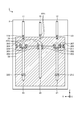
- FIG. 1 is a perspective view showing an example of a schematic configuration of an antenna device according to an embodiment.
- the antenna device 1 shown in FIG. 1 includes a substrate 2, an antenna 10, a parasitic element 11, a parasitic element 12, an antenna 20, a parasitic element 21, a parasitic element 22, and a main plate 30.
- the main plate 30 is shown by hatching.
- XYZ coordinates are shown.
- the Z-axis direction corresponds to the vertical direction
- the X-axis direction and the Y-axis direction correspond to the horizontal direction.
- the substrate 2 is a flat substrate.
- the substrate 2 has a thickness in the X-axis direction, and has a front surface (a surface on the negative direction side of the X-axis) and a back surface (a surface on the positive direction side of the X-axis) extending in the Y-axis direction and the Z direction.
- the term “on the substrate 2” means on the surface of the substrate 2.
- the substrate 2 is, for example, a dielectric substrate having an insulating property.
- the antenna 10 is a first antenna provided on the substrate 2 so as to radiate the first polarized wave.
- the first polarized wave is either a vertically polarized wave or a horizontally polarized wave.
- Vertically polarized waves are electromagnetic waves in which the electric field component in the vertical direction is dominant.
- Horizontally polarized waves are electromagnetic waves in which the electric field component in the horizontal direction is dominant.
- the antenna 10 illustrated in FIG. 1 has a linear shape (rod-shaped) provided on the substrate 2 so as to extend in the positive direction of the Z axis from the base end portion (the portion on the divided main plate 31 side) toward the tip end portion. ) It is a conductive member (for example, a metal pattern).
- the antenna 10 may be a rod-shaped monopole antenna that radiates vertically polarized waves.
- the wavelength of a specific frequency (for example, the center frequency) in the transmission / reception band of the antenna 10 is the wavelength ⁇ 1
- the length of the antenna 10 is set to , for example, 0.25 ⁇ 1.
- the parasitic element 11 and the parasitic element 12 are a pair of parasitic elements provided so as to affect the directivity of the antenna 10.
- the parasitic element 11 and the parasitic element 12 are rod-shaped conductive provided on the substrate 2 so as to extend in the positive direction of the Z axis from the base end portion (the portion on the divided main plate 31 side) toward the tip end portion. It is a sex member.
- the parasitic element 11 and the parasitic element 12 are provided on both sides of the antenna 10 so as to face the antenna 10.
- the parasitic element 11 and the parasitic element 12 are arranged at intervals of, for example, 0.25 ⁇ 1 from the antenna 10.
- the antenna 20 is a second antenna provided on the substrate 2 so as to radiate the second polarized wave.
- the second polarized wave may be polarized wave in the same direction as the first polarized wave radiated by the antenna 10, or may be polarized wave in a direction different from the first polarized wave.
- the antenna 20 illustrated in FIG. 1 is provided on the substrate 2 so as to extend in the negative direction of the Z axis from the base end portion (the portion near the boundary between the split base plate 31 side and the split base plate 32) toward the tip end portion. It is a rod-shaped slot line.
- the antenna 20 is a slot antenna that radiates horizontally polarized waves.
- the antenna 20 is provided so as to be located on the opposite side of the divided main plate 31 from the antenna 10 in the Z-axis direction.
- the wavelength of a specific frequency (for example, the center frequency) in the transmission / reception band of the antenna 20 is the wavelength ⁇ 2
- the length of the antenna 20 is set to , for example, 0.5 ⁇ 2.
- the parasitic element 21 and the parasitic element 22 are a pair of parasitic elements provided so as to affect the directivity of the antenna 20.
- the parasitic element 11 and the parasitic element 22 are rod-shaped slots provided on the substrate 2 so as to extend in the negative direction of the Z axis from the base end portion (the portion on the divided base plate 31 side) toward the tip end portion. It is a railroad track.
- the parasitic element 21 and the parasitic element 22 are provided on both sides of the antenna 20 so as to face the antenna 20.
- the parasitic element 21 and the parasitic element 22 are arranged at intervals of, for example, 0.25 ⁇ 2 from the antenna 20.
- the main plate 30 is a main plate that affects the directivity of the antenna 10 and the antenna 20.
- the main plate 30 includes the divided main plate 31 and the divided main plate 32.
- the divided main plate 31 is a conductive member provided on the substrate 2 so as to affect the directivity of the antenna 10 and / or the antenna 20.
- the divided main plate 31 has a substantially rectangular shape except for a portion where the antenna 20, the parasitic element 21, and the parasitic element 22 are provided.
- the divided base plate 31 is provided so as to face the antenna 10, the parasitic element 11, and the parasitic element 12 in the Z-axis direction.
- the split base plate 31 has a length (length in the Z-axis direction) capable of forming a part of the antenna 20, the parasitic elements 21 and 22 (a portion other than the portion formed by the split base plate 32 described later). Has).
- the divided main plate 32 is a conductive member provided on the substrate 2 so as to affect the directivity of the antenna 10 and / or the antenna 20.
- the divided base plate 32 has a substantially rectangular shape except for a portion where the antenna 20, the parasitic element 21, and the parasitic element 22 are provided.
- the divided main plate 32 is provided so as to face the divided main plate 31 so as to be located on the side opposite to the antenna 10, the parasitic element 11, and the parasitic element 12 with the divided main plate 31 sandwiched in the Z-axis direction.
- the divided base plate 32 may have the same width (length in the Y-axis direction) as the divided base plate 31. Further, the divided base plate 32 has a length (length in the Z-axis direction) capable of forming the antenna 20, the parasitic element 21, and the parasitic element 22.
- the antenna device 1 is provided with a switch group including a plurality of switches. This will be described next with reference to FIG.
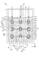
- FIG. 2 is a plan view showing a schematic configuration of the antenna device 1.
- a feeding point FP1, a feeding point FP2, and a switch group are shown.
- the switch group includes a switch 111, a switch 121, a switch 211, a switch 212, a switch 221 and a switch 222, and switches 301 to 308.
- the feeding point FP1 is provided on the substrate portion of the antenna 10 and the divided main plate 31.
- the feeding point FP2 is provided at the base end portion of the antenna 20. Alternatively, it is provided at an arbitrary position along the Z axis of the antenna 20.
- the switch 111 is connected to the parasitic element 11.
- the switch 111 is connected between the base end portion of the parasitic element 11 and the divided base plate 31.
- the switch 111 is SHORT (ON: short circuit)
- the parasitic element 11 is connected to the divided main plate 31.
- the switch 111 is OPEN (OFF)
- the parasitic element 11 is separated from the divided main plate 31.
- the switch 121 is connected to the parasitic element 12.
- the switch 121 is connected between the proximal end of the parasitic element 12 and the split base plate 31.
- the switch 121 is SHORT, the parasitic element 12 is connected to the divided main plate 31.
- the switch 121 is OPEN, the parasitic element 12 is separated from the split base plate 31.
- the switch 211 and the switch 212 are connected to the parasitic element 21.
- the switch 211 is connected between the divided main plates 32 on both sides at the base end portion of the parasitic element 21.
- the switch 211 is SHORT
- the parasitic element 21 becomes a slot line having a length from the base end portion to the switch 211.
- the switch 212 is connected between the divided main plates 32 on both sides at a portion between the base end portion and the tip end portion of the parasitic element 21.
- the switch 211 is OPEN and the switch 212 is SHORT, the parasitic element 21 becomes a slot line having a length from the base end portion to the switch 212. In other words, the slot line from the switch 212 to the tip is invalidated.
- the switch 221 and the switch 222 are connected to the parasitic element 22.
- the switch 221 is connected between the divided main plates 32 on both sides at the base end portion of the parasitic element 22.
- the switch 221 is SHORT
- the parasitic element 21 becomes a slot line having a length from the proximal end to the switch 221.
- the switch 222 is connected between the divided main plates 32 on both sides in the portion between the base end portion and the tip end portion of the parasitic element 22.
- the switch 221 is OPEN and the switch 222 is SHORT
- the parasitic element 22 becomes a slot line having a length from the base end portion to the switch 222. In other words, the slot line from the switch 222 to the tip is invalidated.
- Switch 301 to switch 308 are connected to the main plate 30.
- the switches 301 to 308 are connected in order between the divided base plate 31 and the divided base plate 32 in the Y-axis direction.
- the switch 301 is connected between the split base plate 31 and the split base plate 32 at the ends of the split base plate 31 and the split base plate 32 on the positive direction side of the Y axis.
- the switch 302 is connected between the split base plate 31 and the split base plate 32 at a portion of the base end portion of the parasitic element 22 on the positive direction side of the Y axis.
- the switch 303 is connected between the split base plate 31 and the split base plate 32 at a portion of the base end portion of the parasitic element 22 on the negative direction side of the Y axis.
- the switch 304 is connected between the split base plate 31 and the split base plate 32 at a portion of the base end portion of the antenna 20 on the positive direction side of the Y axis.
- the switch 305 is connected between the split base plate 31 and the split base plate 32 at a portion of the base end portion of the antenna 20 on the negative direction side of the Y axis.
- the switch 306 is connected between the split base plate 31 and the split base plate 32 at a portion of the base end portion of the parasitic element 21 on the positive direction side of the Y axis.
- the switch 307 is connected between the split base plate 31 and the split base plate 32 at a portion of the base end portion of the parasitic element 21 on the negative direction side of the Y axis.
- the switch 308 is connected between the divided base plate 31 and the divided base plate 32 at the ends of the divided base plate 31 and the divided base plate 32 on the negative direction side of the Y axis.
- a part of the antenna 20 may be formed of the divided main plate 31, and in this case, the switch 304 and the switch 305 are formed of the portion formed by the divided main plate 31 of the antenna 20 and the divided main plate 32. Connect with the part.
- a part of the parasitic element 21 may be formed of the divided base plate 31, and in this case, the switch 306 and the switch 307 connect the portion of the parasitic element 21 formed of the divided base plate 31 and the portion formed of the divided base plate 32.
- a part of the parasitic element 22 may be formed of the divided base plate 31, and in this case, the switch 302 and the switch 303 connect the portion of the parasitic element 22 formed of the divided base plate 31 and the portion formed of the divided base plate 32. do.
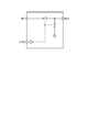
- FIG. 3 is a diagram showing an example of a schematic configuration of SPST.
- the OPEN / SHORT between the terminal RF1 and the terminal RF2 is switched. Switching is controlled by the control signal CTRL. It is also possible to switch so that the terminal RF2 is connected to the ground.
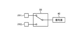
- Example of power feeding method An example of a power feeding method using the power feeding point FP1 and the feeding point FP2 will be described with reference to FIGS. 4A to 4C.
- the power supply system shown in FIG. 4A is an example of a switching diversity scheme.
- the signal source 40 produces a transmit RF signal.
- the transmitted RF signal generated by the signal source 40 is selectively supplied to either the feeding point FP1 or the feeding point FP2 via the switch 50.
- the switch 50 for example, SPDT (Single Pole Double Through) may be used.
- FIG. 5 is a diagram showing an example of a schematic configuration of SPDT. In the SPDT illustrated in FIG.
- the DRIVER switches between the OPEN / SHORT between the terminal RFC and the terminal RF1 and the OPEN / SHORT between the terminal RFC and the terminal RF2 according to the control signal CTRL.
- the DRIVER operates according to the power supply voltage VSS and the power supply voltage VDD. Similarly, it can be a switching diversity in reception.
- the power supply system shown in FIG. 4B is an example of a synthetic diversity scheme.
- the transmission RF signal generated by the signal source 40 is supplied to the feeding point FP1 after being phase-shifted by phase ⁇ 1 by the phase shifter 61, and is supplied to the feeding point FP2 after being phase-shifted by phase ⁇ 2 by the phase shifter 62.
- the antenna 10 and the antenna 20 radiate polarized waves orthogonal to each other, a radiation pattern in which polarization and directivity are combined can be formed.
- it can be a synthetic diversity in reception.
- the power supply method shown in FIG. 4C is an example of MIMO (Multiple Input Multiple Output).
- the signal source 41 and the signal source 42 generate different transmission RF signals.
- the transmission RF signal generated by the signal source 41 is supplied to the feeding point FP1.
- the transmitted RF signal generated by the signal source 42 is supplied to the feeding point FP2.
- MIMO with low correlation and high S / N is realized. Similarly, it can be MIMO in reception.
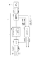
- FIG. 6 is a diagram showing an example of a schematic configuration of an antenna device and an electronic device constituting such a control system.
- the antenna device 1 includes an RF signal processing block 400, a switching control block 500, and a modulation / demodulation signal processing block 600 in addition to the configurations described so far.
- the antenna device 1 is mounted on the electronic device 5, and a portion of the electronic device 5 other than the antenna device 1 is shown as another block 700.
- the power feeding scheme is a switching diversity scheme (FIG. 4A).
- the other block 700 is configured to supply transmission data to the modulation / demodulation signal processing block 600 of the antenna device 1 and to receive received data from the modulation / demodulation signal processing block 600.
- the modulation / demodulation signal processing block 600 generates a modulated signal based on the transmitted data.
- the RF signal processing block 400 generates a transmit RF signal based on the modulated signal.
- the generated transmission RF signal is supplied to the feeding point FP1 or the feeding point FP2 (FIG. 2) of the antenna device 1 via the switch 50.
- the received RF signal is supplied from the antenna device 1 to the RF signal processing block 400 via the switch 50.
- the RF signal processing block 400 processes the received RF signal (amplification, filtering, frequency conversion, etc.).
- the modulation / demodulation signal processing block 600 demodulates the processed received RF signal to obtain received data.
- an index related to transmission / reception is sent to the switching control block 500.
- indicators are reception level information (RSSI: Received Signal Strength Indicator), transmission level information, reception QoS (Quality of Service) information (SIR: signal-to-interference ratio, BER: Bit Error Rate), and transmission QoS information. Yes, but not limited to these.
- the changeover control block 500 generates a changeover signal for controlling each of the switch 50, the switch 111, the switch 121, the switch 211, the switch 212, the switch 221, the switch 222, the switch 301 to the switch 308 (FIG. 2), and the switch 50. do.
- the switching signal is generated based on the above-mentioned index sent from the modulation / demodulation signal processing block 600.
- the switching control block 500 generates a switching signal so that at least one index of each of the above-mentioned indexes is maximized.
- the antenna device 1 has various states as described below due to the switching control by the switching control block 500.
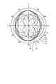
- FIG. 7 is a diagram showing an example of State.
- FIG. 7 shows 24 types of States from State 00 to State 23. “ON” means that power is supplied to the antenna by the corresponding feeding point, and “OFF” means that power is not supplied. “OPEN” means that the corresponding switch is in a non-conducting state (open), and “SHORT” means that it is in a conductive state (short circuit).
- States00 to State05 are examples in which power is supplied (excited) only to the antenna 10 and the switches connected to the parasitic element 11, the parasitic element 12, the divided base plate 31 and the divided base plate 32 are switched.
- States 06 to 08 are examples in which power is supplied only to the antenna 20 and the switch connected to the parasitic element 21 and the parasitic element 22 is switched.
- the State 09 and the State 10 are examples in which power is supplied only to the antenna 10 and the switches connected to the parasitic element 21, the parasitic element 22, the divided base plate 31 and the divided base plate 32 are switched.
- States 11 to 23 are examples in which power is supplied only to the antenna 20 and switches connected to the parasitic element 11, the parasitic element 12, the parasitic element 21, and the parasitic element 22 are switched.
- State00 to State23 various States can be obtained.
- Examples include a State that switches each one independently.
- Lengths of the parasitic element 11 in the Y and Z axis directions 10 mm and 80 mm, respectively.
- Lengths of the parasitic element 12 in the Y and Z axis directions 10 mm and 80 mm, respectively.
- Distance between the antenna 10 and the parasitic element 11 in the Y-axis direction 75 mm.
- Distance between the antenna 10 and the parasitic element 12 in the Y-axis direction 75 mm.
- Lengths of antenna 20 in the Y and Z axis directions (of slots) 10 mm and 170 m, respectively.
- Lengths of the parasitic element 21 in the Y and Z axis directions 10 mm and 190 m, respectively.
- Lengths of the parasitic element 22 in the Y and Z axis directions 10 mm and 190 m, respectively.
- Distance between switch 222 and switch 222 in the Z-axis direction 5 mm.
- Distance between the antenna 20 and the parasitic element 21 in the Y-axis direction 75 mm.
- Distance between the antenna 20 and the parasitic element 22 in the Y-axis direction 75 mm.
- Lengths of the divided base plate 31 in the Y and Z axis directions 250 mm and 45 mm, respectively.
- Lengths of the divided base plate 32 in the Y and Z axis directions 250 mm and 200 mm, respectively.
- Distance between the divided base plate 31 and the divided base plate 32 in the Z-axis direction 5 mm.
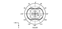
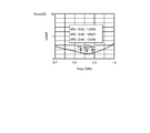
- FIGS. 8A to 8C show the simulation results of State00 to State02.
- the solid line shows the gain of vertically polarized waves (dBi)
- the broken line shows the gain of horizontally polarized waves
- the thick solid line shows the total gain (dBi).
- the radiation of vertically polarized waves in the Y-axis direction is dominant. This is because the antenna 10, the parasitic element 11, and the parasitic element 12, which are conductive members, are provided side by side in the Y-axis direction.
- State02 (FIG. 8C) has a larger gain in the positive direction of the Y-axis than State00 (FIG. 8A). This is because, of the parasitic element 11 and the parasitic element 12, only the parasitic element 12 is connected to the divided main plate 31 by the switch 121, so that the parasitic element 12 operates as a reflecting element.
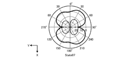
- FIGS. 9A to 9C show the simulation results of State06 to State08.
- the solid line shows the gain of vertically polarized waves (dBi)
- the broken line shows the gain of horizontally polarized waves
- the thick solid line shows the total gain (dBi).
- the radiation of horizontally polarized waves in the X-axis direction is dominant. This is because the antenna 20, the parasitic element 21, and the parasitic element 22, which are slot lines, are provided side by side in the Y-axis direction.
- the State 00 to State 02 and the State 06 to State 08 described above are directional by switching the polarization by switching between the antenna 10 and the antenna 20, and by switching the switch 111, the switch 121, the switch 211, the switch 212, the switch 221 and the switch 222. This is an example of control. In addition to this, those skilled in the art can understand that the directivity is also controlled by switching the switch 301 to the switch 308.
- FIG. 10 shows a contrast between State 01 and State 03.
- the solid line shows the total gain (dBi) of State 1
- the broken line shows the total gain (dBi) of State 03.
- the State 03 realizes a directivity different from that of the State 01. This is because in State 03, the current flowing through the main plate 30 and the divided main plate 31 changes because the divided main plate 31 and the divided main plate 32 are connected by the switches 301 to 308 and the pattern of the main plate 30 is changed. ..
- the antenna device 1 can have various States having different polarization and directivity.
- the State of the antenna device 1 is controlled by the switching control block 500 described above with reference to FIG.
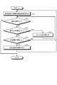
- FIG. 11 is a flowchart showing an example of switching control processing (control method of the antenna device 1). This process is repeatedly executed by the switching control block 500, for example, while transmission / reception (use of the electronic device 5) by the antenna device 1 is being performed.
- step S1 the switching control block 500 acquires an index related to transmission / reception. For example, as described above with reference to FIG. 6, indexes such as reception level information (RSSI), transmission level information, reception QoS information (SIR, BER), and transmission QoS information are acquired.
- RSSI reception level information
- SIR transmission level information
- BER reception QoS information
- transmission QoS information transmission QoS information
- step S2 the switching control block 500 determines whether or not a predetermined condition is satisfied. For example, when searching for a State in which the best index can be obtained, it is determined that a predetermined condition is satisfied when the index acquired in the previous step S1 is better than the index acquired in step S1 of the previous loop. You can do it. Alternatively, if a State that satisfies a certain index is sufficient, it may be determined that the predetermined condition is satisfied when the index acquired in the previous step S1 exceeds the threshold value. In addition to this, various conditions may be used as predetermined conditions. When the predetermined condition is satisfied (Yes in step S2), the processing of the flowchart ends. If the predetermined condition is not satisfied (No in step S2), the process is returned to step S1 again via step S3.
- step S3 the changeover control block 500 switches the switch. Which switch is to be switched may be appropriately determined. For example, each switch may be switched so that State 00 to State 23 described above are sequentially realized each time steps S1 to S3 are looped.
- the antenna device 1 can be switched to the State where the desired directivity can be obtained.
- FIG. 12 is a plan view showing a schematic configuration of an antenna device according to such a modification.
- the antenna device 1A shown in FIG. 12 is different from the antenna device 1 (FIG. 2) in that the position of the feeding point of the antenna 20 is different.
- the two feeding points FP2A1 and the feeding point FP2A2 are provided at arbitrary positions of the antenna 20.
- the number and position of the feeding point FP2A1 and the feeding point FP2A2 are examples, and various other feeding points may be provided at various positions.
- FIG. 13 is a plan view showing a schematic configuration of an antenna device according to such a modification.
- the antenna device 1B shown in FIG. 13 is different from the antenna device 1 (FIG. 2) in that the split base plate 32B is provided instead of the split base plate 32 and that the switches 309 to 316 are provided.
- the divided base plate 32B is divided into five parts: a first part 321, a second part 322, a third part 323, a fourth part 324, and a fifth part 325. Each part is connected by switches 309 to 316.
- the first portion 321 and the second portion 322 are provided between the antenna 20 and the parasitic element 21 in order from the base end portion to the tip end portion of the antenna 20 (in the negative direction of the Z axis).
- the first portion 321 and the second portion 322 have a substantially rectangular shape.
- the switch 309 is connected between the first portion 321 and the second portion 322 in the vicinity of the parasitic element 21.
- the switch 310 is connected between the first portion 321 and the second portion 322 in the vicinity of the antenna 20.
- the third portion 323 and the fourth portion 324 are sequentially provided between the antenna 20 and the parasitic element 22 in the direction from the base end portion to the tip end portion of the antenna 20.
- the third portion 323 and the fourth portion 324 have a substantially rectangular shape.
- the switch 311 is connected between the third portion 323 and the fourth portion 324 in the vicinity of the antenna 20.
- the switch 312 is connected between the third portion 323 and the fourth portion 324 in the vicinity of the parasitic element 22.
- the fifth portion 325 is a portion of the divided base plate 32 other than the first portion 321 to the fourth portion 324.
- the portion provided between the antenna 20 and the parasitic element 21 is connected to the second portion 322 via the switch 313 and the switch 314.
- the switch 313 is connected between the second portion 322 and the fifth portion 325 in the vicinity of the parasitic element 21.
- the switch 314 is connected between the second portion 322 and the fifth portion 325 in the vicinity of the antenna 20.
- the portion provided between the antenna 20 and the parasitic element 22 is connected to the fourth portion 324 via the switch 315 and the switch 316.
- the switch 315 is connected between the fourth portion 324 and the fifth portion 325 in the vicinity of the parasitic element 22.
- the switch 316 is connected between the fourth portion 324 and the fifth portion 325 in the vicinity of the parasitic element 22.
- the switch 309 to 316 are switched by the changeover control block 500 (FIG. 6). By switching the switch 309 to 316, the pattern of the divided base plate 32B is changed, thereby obtaining different directivity.
- the division pattern and connection relationship of the division base plate 32B are not limited to the example shown in FIG.
- FIG. 14 is a plan view showing a schematic configuration of an antenna device according to such a modification.
- the antenna device 1C shown in FIG. 14 has a parasite 10, a parasitic element 11, a parasitic element 12, an antenna 20, a parasitic element 21, a parasitic element 22, a switch 212, and a switch 222, as compared with the antenna device 1 (FIG. 2).
- the antenna 10C is different from the antenna 10 (FIG. 2) in that the switch 101 and the feeding point FP1C0 are provided at the base end portion.
- the switch 101 is provided in parallel with the feeding point FP1C0.
- the switch 101 is switched by the switching control block 500 (FIG. 6). By setting the switch 101 to SHORT, the antenna 10C can be used as a parasitic element instead of exciting the antenna 10C via the feeding point FP1C0.
- the parasitic element 11C is different from the parasitic element 11 (FIG. 2) in that a feeding point FP1C1 is provided at the base end portion.
- the switch 111 is provided in parallel with the feeding point FP1C1. By setting the switch 111 to OPEN, the parasitic element 11C can be excited via the feeding point FP1C1 and the parasitic element 11C can be used as an antenna.
- the parasitic element 12C is different from the parasitic element 12 (FIG. 2) in that a feeding point FP1C2 is provided at the base end portion.
- the switch 121 is provided in parallel with the feeding point FP1C2. By setting the switch 121 to OPEN, the parasitic element 12C can be excited via the feeding point FP1C2, and the parasitic element 12C can be used as an antenna.
- the antenna 20C is different from the antenna 20 (FIG. 2) in that the feeding point FP2C0 is provided instead of the feeding point FP2.
- the feeding point FP2C0 is not limited to the proximal end portion of the antenna 20, and is provided at an arbitrary position of the antenna 20.
- the switch 201C is connected in parallel with the feeding point FP2C0. That is, the switch 201C is connected between the divided main plates 32 at both ends of the antenna 20C.
- the switch 201C is switched by the switching control block 500 (FIG. 6). By setting the switch 201C to SHORT, the antenna 20C can be used as a parasitic element instead of exciting the antenna 20C via the feeding point FP2C1.
- the parasitic element 21C is different from the parasitic element 21 (FIG. 2) in that the feeding point FP2C1 is provided and that the switch 212C is provided instead of the switch 212.
- the feeding point FP2C1 is provided at an arbitrary position of the parasitic element 21C.
- the switch 212C is connected in parallel with the feeding point FP2C1. That is, the switch 212C is connected between the divided main plates 32 at both ends of the parasitic element 21.
- the switch 212C is switched by the switching control block 500 (FIG. 6).
- the switch 212C is set to OPEN, the parasitic element 21C can be excited via the feeding point FP2C1 and the parasitic element 21C can be used as an antenna.
- the parasitic element 22C is different from the parasitic element 22 (FIG. 2) in that the feeding point FP2C2 is provided and that the switch 222C is provided instead of the switch 222.
- the feeding point FP2C2 is provided at an arbitrary position of the parasitic element 22C.
- the switch 222C is connected in parallel with the feeding point FP2C2. That is, the switch 222C is connected between the divided main plates 32 at both ends of the parasitic element 22C.
- the switch 222C is switched by the switching control block 500 (FIG. 6).
- the switch 222C is set to OPEN, the parasitic element 22C can be excited via the feeding point FP2C2, and the parasitic element 22C can be used as an antenna.
- FIG. 15 is a plan view showing a schematic configuration of an antenna device according to such a modification.
- the antenna device 1D shown in FIG. 15 includes an antenna 10D, a parasitic element 11D, and a parasitic element 12D in place of the antenna 10, the parasitic element 11, and the parasitic element 12. It's different.
- the antenna 10D is different from the antenna 10 (FIG. 2) in that it is a foldable antenna having a foldable portion.
- the antenna 10D has a portion extending in the positive direction of the Z axis from the base end portion, two portions bent from the portion extending in the positive direction of the Y axis and extending in the negative direction of the Y axis, and further from them. It has a portion that is bent and extends in the negative direction of the Z axis.
- the parasitic element 11D includes a portion extending in the Z-axis positive direction from the base end portion, a portion bent from the base end portion extending in the Y-axis positive direction, and a portion further bent from there and extending in the Z-axis negative direction.
- the parasitic element 12D includes a portion extending in the positive direction of the Z axis from the base end portion, a portion bent from there and extending in the negative direction of the Y axis, and a portion bent from there and extending in the negative direction of the Z axis.
- the bent shape of the antenna 10D, the parasitic element 11D, and the parasitic element 12D makes the antenna device 1D more compact than the antenna device 1.
- the shapes of the antenna 10D, the parasitic element 11D, and the parasitic element 12D may be any shape as long as they can shorten the length in the Z-axis direction, and are not limited to the example shown in FIG.
- the antenna 10D may have a curved portion instead of the bent portion, or may have both a bent portion and a curved portion.
- FIG. 16 is a plan view showing a schematic configuration of an antenna device according to such a modification.
- the antenna device 1E shown in FIG. 16 is different from the antenna device 1 (FIG. 2) in that it includes a variable reactance element 111E and a variable reactance element 121E in place of the switch 111 and the switch 121.
- the variable reactance element 111E and the variable reactance element 121E are one aspect of the switches constituting the switch group.
- variable reactance element 111E and the variable reactance element 121E exemplified are capacitors capable of changing the capacitance value such as a varicap.
- the capacitance values of the variable reactance element 111E and the variable reactance element 121E are controlled by the switching control block 500 (FIG. 6).
- Different directivity can also be obtained by changing the reactance values of the variable reactance element 111E and the variable reactance element 121E to switch the connection state between the parasitic element 11 and the divided base plate 31.
- FIG. 17 is a plan view showing a schematic configuration of an antenna device according to such a modification.
- the antenna device 1F shown in FIG. 17 includes a parasitic element 21F and a parasitic element 22F instead of the parasitic element 21 and the parasitic element 22, and the switch 213F and the switch 223F. It differs in that it is provided.
- the switch 213F is provided at an arbitrary position between the switch 211 and the switch 212 on the parasitic element 21F.
- the switch 213F is connected between the divided main plates 32 on both sides of the parasitic element 21F.
- the parasitic element 21 has a line length of the length from the proximal end to the switch 214.
- the switch 223F is provided at an arbitrary position between the switch 221 and the switch 222 on the parasitic element 22F.
- the switch 223F is connected between the divided main plates 32 on both sides of the parasitic element 22.
- the parasitic element 22 has a line length of the length from the proximal end to the switch 224.
- Different directivity can also be obtained by finely switching the lengths of the parasitic element 21F and the parasitic element 22F by the switch 213F and the switch 223F.
- additional switches may be added.
- the radiation pattern can be freely changed with various combinations other than those described above, such as the combination of excitation with vertically polarized waves and parasitic elements with horizontally polarized waves, to further optimize communication performance. can do. It is also possible to make each element multi-band. It is also possible to mount an antenna tuning element to widen the band.
- FIG. 18 is a diagram showing an example of a schematic configuration of an antenna device according to a second embodiment.
- the antenna device 1G shown in FIG. 18 is different from the antenna device 1 (FIG. 2) in that the antenna 20G and the main plate 33 are provided in place of the antenna 20 and the main plate 30.
- the antenna device 1G is shown in a mode that does not have the parasitic element 21 and the parasitic element 22 as in the antenna device 1 (FIG. 2), but has a configuration corresponding to such a parasitic element 21 and the parasitic element 22. You may have it.
- the antenna 20G is a second antenna provided on the substrate 2 so as to radiate the second polarized wave.
- the second polarized wave radiated by the antenna 20G is a polarized wave in the same direction as the first polarized wave radiated by the antenna 10.
- the antenna 20G illustrated in FIG. 18 is a slot antenna provided on the substrate 2 so as to extend in the horizontal direction, and emits vertically polarized waves.
- the feeding point FP2G of the antenna 20G may be provided at an arbitrary position of the antenna 20G.
- the main plate 33 is provided on the substrate 2 so as to have an area (pattern length and pattern width) that can affect the radiation characteristics of the antenna 10 and / or 20G.
- the main plate 33 has a substantially rectangular shape except for a portion where the antenna 20G is provided.
- the main plate 33 has a length (length in the Y-axis direction) capable of forming the antenna 20G.
- the antenna 20G is excited via the feeding point FP2G.
- the antenna device 1G also has various States as described below by the switching control block 500 (FIG. 6).
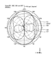
- FIG. 19 is a diagram showing an example of State.
- Beam orientation indicates the direction of directivity.
- Y- corresponds to the negative direction of the Y axis.
- Y + corresponds to the positive direction of the Y axis.
- X ⁇ corresponds to the positive direction of the X axis and the negative direction of the X axis.
- eight types of Stages 200 to 207 can be obtained.
- Lengths of the parasitic element 11 in the Y and Z axis directions 2 mm and 67 mm, respectively.
- Lengths of the parasitic element 12 in the Y and Z axis directions 2 mm and 67 mm, respectively.
- Distance between the antenna 10 and the parasitic element 11 in the Y-axis direction 88 mm.
- Distance between the antenna 10 and the parasitic element 12 in the Y-axis direction 88 mm.
- Lengths (of slots) of antenna 20 in the Y and Z axes, respectively 200 and 4 mm.
- Distance from one end of the antenna 20 in the Y-axis direction to the feeding point FP2G 60 mm.
- Lengths of the main plate 33 in the Y and Z axis directions 209 mm and 150 mm, respectively.
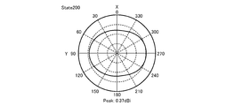
- 20A to 20E show the simulation results of State200.
- 20A to 20C show the directivity when viewed in the XY plane, the XZ plane, and the YZ plane.
- directivity is obtained especially in the Y-axis direction. This is because the antenna 10, the parasitic element 11, and the parasitic element 12, which are conductive members, are provided side by side in the Y-axis direction. Further, almost symmetrical directivity can be obtained in the X-axis direction and the Y-axis direction. This is because the parasitic element 11 and the parasitic element 12 are both separated from the main plate 33 by the switch 111 and the switch 121, and the influence of the parasitic element 11 and the parasitic element 12 on the antenna 10 is small.
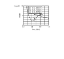
- FIG. 20D shows the radiation efficiency (dB) and FIG. 20E shows VSWR.
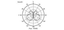
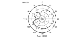
- FIGS. 21A to 21E show the simulation results of State201.
- the gain in the negative direction of the Y axis is larger in the State 201 than in the State 200 (FIGS. 20A to 20C).
- the parasitic element 11 and the parasitic element 12 only the parasitic element 11 is connected to the main plate 33 by the switch 111, so that the parasitic element 11 operates as a reflecting element.
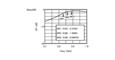
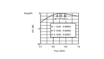
- markers M11 to M13 in FIGS. 21D and 21E good radiation efficiency and VSWR are still obtained at frequencies of 0.83 GHz to 0.89 GHz.
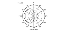
- FIGS. 22A to 22E show the simulation results of State202.
- the gain in the positive direction of the Y-axis is larger in the State 202 than in the State 200 (FIGS. 20A to 20C).
- the parasitic element 11 and the parasitic element 12 only the parasitic element 12 is connected to the main plate 33 by the switch 121, so that the parasitic element 12 operates as a reflecting element.
- markers M21 to M23 in FIGS. 22D and 22E good radiation efficiency and VSWR are still obtained at frequencies of 0.83 GHz to 0.89 GHz.
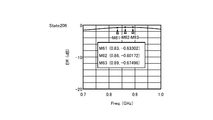
- FIGS. 23A to 23E show the simulation results of State 203.
- the gains in the X-axis direction and the Y-axis positive direction change as compared with the State 200 (FIGS. 20A to 20C). It is considered that this is because the parasitic element 11 and the parasitic element 12 are connected to the main plate 33 by the switch 111 and the switch 121, so that the influence of the parasitic element 11 and the parasitic element 12 on the antenna 10 is changed.
- markers M31 to M33 in FIGS. 23D and 23E changes also occur in radiation efficiency and VSWR at frequencies of 0.83 GHz to 0.89 GHz.
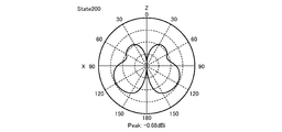
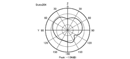
- FIGS. 24A to 24E show the simulation results of State204.
- State 204 directivity is obtained particularly in the X-axis direction. This is because the antenna 20G, which is a slot line, is provided in the Y-axis direction. Further, almost symmetrical directivity can be obtained in the X-axis direction and the Y-axis direction. This is because the main plate 33 is separated from the parasitic element 11 and the parasitic element 12 by the switch 111 and the switch 121, and the influence of the parasitic element 11 and the parasitic element 12 on the antenna 20G is small. As shown by markers M41 to M43, good radiation efficiency and VSWR are still obtained at frequencies of 0.83 GHz to 0.89 GHz.
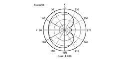
- 25A to 25E show the simulation results of State 205.
- the gain in the positive direction of the Y-axis is larger in the State 205 than in the State 204 (FIGS. 24A to 24C). It is considered that this is because the main plate 33 is connected to the parasitic element 11 by the switch 111, and the influence of the parasitic element 11 on the antenna 20G has changed.
- markers M51 to M53 good radiation efficiency and VSWR are still obtained at frequencies of 0.83 GHz to 0.89 GHz.
- FIGS. 26A to 26E show the simulation results of State 206.
- the gain in the X-axis direction and the Y-axis direction changes in the State 206 as compared with the State 204 (FIGS. 24A to 24C). It is considered that this is because the main plate 33 is connected to the parasitic element 12 by the switch 121, and the influence of the parasitic element 12 on the antenna 20G has changed.
- markers M61 to M63 good radiation efficiency and VSWR are still obtained at frequencies of 0.83 GHz to 0.89 GHz.
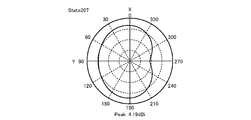
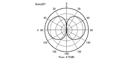
- FIGS. 27A to 27E show the simulation results of State 207.
- the gain in the positive direction of the Y axis is larger than that in State 204 (FIGS. 24A to 24C). It is considered that this is because the main plate 33 is connected to the parasitic element 11 and the parasitic element 12 by the switch 111 and the switch 121, so that the influence of the parasitic element 11 and the parasitic element 12 on the antenna 20G is changed.
- markers M71 to M73 good radiation efficiency and VSWR are still obtained at frequencies of 0.83 GHz to 0.89 GHz.
- FIG. 28 shows a contrast between State 200 to State 207.
- Curves C0 to C7 show the gains of State 200 to State 207.
- a gain of ⁇ 5 dBi can be obtained in all directions of 360 degrees by switching between State 200 to State 207.
- FIG. 29 is a diagram showing a prototype. As shown in FIG. 29, in the prototype, the antenna 10 was excited from the port PORT1 via the transmission line LINE1 (and the feeding point FP1). The antenna 20G was excited from the port PORT2 via the transmission line LINE2 (feeding point FP2).
- the transmission line LINE1 and the transmission line LINE2 are microstrip lines in this example. However, in addition to the microstrip line, a coplanar line, a strip line, or the like may be used. Since the substrate 2, the antenna 10, the antenna 20G, and the main plate 33 are the same as the above simulation conditions, the description will not be repeated here.
- FIG. 30A shows the experimental results of State 201.
- the solid line shows the directivity at a frequency of 830 MHz.
- the thick solid line indicates the directivity at a frequency of 860 MHz.
- the broken line indicates the directivity at a frequency of 890 MHz.
- FIG. 30B shows the experimental results of State202. Experimental results close to the simulation results described above with reference to FIG. 22A and the like were obtained.
- FIG. 30C shows the experimental results of State204. Experimental results close to the simulation results described above with reference to FIG. 24A and the like were obtained.
- FIG. 31 shows the experimental results of State201, State202, State206 and State207.
- Curve C1, curve C2, curve C6 and curve C7 show the directivity of State201, State202, State206 and State207.
- the curved CREF indicates the directivity of a commercially available sleeve dipole antenna (almost omnidirectional antenna). For example, when viewed on the XY plane, it was confirmed that a gain of ⁇ 5 dBi can be obtained in all directions of 360 degrees by switching State201, State202, State206, and State207.
- FIG. 32 is a plan view showing a schematic configuration of an antenna device according to such a modification.
- the antenna device 1H shown in FIG. 32 is different from the antenna device 1G (FIG. 18) in that it includes an antenna 10H1 and an antenna 10H2 instead of the antenna 10 and a hybrid element 90.
- Both the antenna 10H1 and the antenna 10H2 are monopole antennas extending in the positive direction of the Z axis.
- the hybrid element 90 is a 90-degree hybrid element, and distributes signals from the feeding point FP1H to supply signals having different phases of 90 ° to the antenna 10H1 and the antenna 10H2, respectively.
- the antenna 10 may be excited in the first frequency band (eg 800 MHz band) and the antenna 20 may be excited in the second frequency band (eg 2 GHz band).
- the signal in the first frequency band is radiated by the antenna 10 with directivity in the Y-axis direction.
- the signal in the second frequency band is radiated by the antenna 20 with directivity in the X-axis direction. Therefore, the antenna device 1H functions as a direct beam antenna in which the directivity of different frequency bands constituting the multi-band is orthogonal. Further, by using a pair of antennas, the antenna device 1H can be made smaller than the configuration having two elements of the parasitic element 11 and the parasitic element 12.
- FIG. 33 is a plan view showing a schematic configuration of an antenna device according to such a modification.
- the antenna device 1J shown in FIG. 33 includes an antenna 10J1 and an antenna 10J2 instead of the antenna 10H1 and the antenna 10H2, and a switch 101J1 and a switch 101J2.
- the difference is that the hybrid element 90 is not provided.
- the switch 101J1 is a SPDT switch connected between the antenna 10J1, the main plate 33, and the switch 101J3.
- the switch 101J1 switches between a state in which the antenna 10J1 is connected to the main plate 33 and a state in which the antenna 10J1 is connected to the switch 101J3.
- the switch 101J1 is switched by the switching control block 500 (FIG. 6).
- the switch 101J2 is a SPDT switch connected between the antenna 10J2, the main plate 33, and the switch 101J3.
- the switch 101J2 switches between a state in which the antenna 10J2 is connected to the main plate 33 and a state in which the antenna 10J2 is connected to the switch 101J3.
- the switch 101J2 is switched by the switching control block 500 (FIG. 6).
- the switch 101J3 is a SPDT switch connected between the switch 101J2, the switch 101J2, and the signal source 40 (see FIG. 4A and the like).
- the switch 101J3 switches between a state in which the switch 101J1 is connected to the signal source 40 (excited state) and a state in which the switch 101J2 is connected to the signal source 40 (excited state).
- the use of the antenna 10J1 and the antenna 10J2 can be switched between the antenna and the parasitic element.
- the antenna device 1J can be made smaller than the configuration having two elements, the parasitic element 11 and the parasitic element 12.
- the antenna device 1G according to the second embodiment can be modified in the same manner as the antenna device 1 according to the first embodiment.
- the parasitic element 21 and the parasitic element 22 for the antenna 20 as described above with reference to FIG. 2 may be provided for the antenna 20G of the antenna device 1G.
- These parasitic elements may be provided so as to extend along the extending direction (Y-axis direction) of the antenna 20G.
- the modification described above with reference to FIGS. 11 to 17 may be applied to the substrate 2G.
- FIG. 34 is a plan view showing an example of a schematic configuration of an antenna device according to such a modified example.
- the antenna device 1K shown in FIG. 34 includes an antenna 20K, a parasitic element 21K, a parasitic element 22K, an antenna 23K, a parasitic element 24K, and a parasitic element 25K as slot lines formed by the main plate 34.
- the antenna 20K is a slot antenna extending in the Z-axis direction, and is excited via the feeding point FP2.
- the parasitic element 21K and the parasitic element 22K are provided on both sides of the antenna 20K.
- the antenna 23K is a slot antenna extending in the Y-axis direction, and is excited via the feeding point FP3K.
- the parasitic element 24K and the parasitic element 25K are provided on both sides of the antenna 23K.
- the feeding point FP2K is arranged at an arbitrary position along the antenna 20K, and the feeding point FP3K is arranged at an arbitrary position along the antenna 23K. However, it is desirable to avoid the inside of the parasitic slot.
- the antenna device 1K includes switches 251 to 262 as switches for switching the lengths of the antenna 20K, the parasitic element 21K, the parasitic element 22K, the antenna 23K, the parasitic element 24K, and the parasitic element 25K.
- switches 251 to 262 are provided so as to surround the intersection of the slot lines.
- the arrangement of the switches is not limited to the example of FIG. 34.
- the antenna device 1K also has various States as described below by the switching control block 500 (FIG. 6).
- FIG. 35 is a diagram showing an example of State. “V” indicates vertically polarized waves, and “H” indicates horizontally polarized waves. As shown in FIG. 35, the States 300 to 308 in which the polarization and the directivity are switched can be obtained. Not limited to the example shown in FIG. 35, various states can be obtained by individually switching each feeding point and switch.
- the components of the antenna device 1 such as the antenna, the parasitic element, the main plate, and the switch group are provided on the surface of the substrate 2 has been described.
- a part or all of the components of the antenna device 1 may be provided on the back surface of the substrate 2.
- the frequency band of the antenna device according to the embodiment is not limited to the 800 MHz and 2 GHz bands. Examples of other frequency bands are the 2.4 GHz band, the 5 GHz band, and even the millimeter wave band, which is a higher frequency band.
- the antenna device according to the embodiment may be applied to radio waves in any frequency band including these.
- Antenna devices may be applied to any wireless system that utilizes those frequency bands. Examples of wireless systems are LTE (Long Term Evolution), UWB (Ultra Wide Band), WiFi (registered trademark), and the like.
- Antenna devices can be applied to any application that utilizes those frequency bands or wireless systems. Examples of applications are telephone calls, data communications, distance measurement, positioning, motion sensing, and the like.
- each switch or the like is set based on indexes such as reception level information (RSSI), transmission level information, reception QoS information (SIR, BER), and transmission QoS information.
- RSSI reception level information
- SIR reception QoS information
- BER reception QoS information
- transmission QoS information transmission QoS information
- the transmission level information may include transmission power and the like.
- the received QoS information may include an indicator included in the packet and the like. The same applies to the transmitted QoS information.
- Many wireless transmission / reception signals include an indicator indicating the quality of the signal in the packet.
- An example of an indicator is a numerical value determined according to the level of quality. Examples of numerical values are numerical value 1 indicating that the quality is good (Good Quality), numerical value 2 indicating that the quality is low (Low Quality), and unreliable (for any) that the reliability is low due to some reason such as loss of a signal. Reason like Signal Lost, etc)), and a numerical value 4 indicating that the quality is unknown (Unknown quality).
- the information regarding the frequency characteristics includes the information regarding the frequency characteristics of the received signal and the frequency characteristics of the transmitted signal.
- Examples of information regarding the frequency characteristics of the received signal are the frequency characteristics of the phase or amplitude of the received signal and the information based on the frequency characteristics (gradient value, moving average value, etc.).
- Examples of information regarding the frequency characteristics of the transmission signal are the frequency characteristics of the phase or amplitude of the transmission signal and information based on the frequency characteristics (gradient value, moving average value, etc.).
- the phase or amplitude may be a relative value relative to the phase or amplitude at a certain frequency. Such an index will be described with reference to FIGS. 36A to 36C.
- FIGS. 36A to 36C are diagrams schematically showing an example of information regarding frequency characteristics.
- FIGS. 36A and 36B show examples of phase or amplitude frequency characteristics at different States.
- the horizontal axis of the graph indicates frequency, and the vertical axis indicates phase or amplitude.
- the frequency range is the transmission / reception frequency band of the antenna (for example, 2.4 GHz to 2.48 GHz, etc.).
- the phase or amplitude changes to decrease at a substantially constant rate as the frequency increases.
- FIG. 36B as the frequency increases, the phase or amplitude changes repeatedly and irregularly.
- the frequency characteristics of the phase or amplitude of the transmission signal or the reception signal can also be used as an index.
- control may be performed such as selecting a State whose frequency characteristics satisfy a predetermined condition, selecting a State having the optimum frequency characteristics, and selecting a State having the minimum variation in the frequency characteristics.
- FIG. 36C shows an example of the slope value of the frequency characteristic of the phase or amplitude in each of the different States.
- Graph line A shows the slope value of the frequency characteristic shown in FIG. 36A described above.
- Graph line B shows the slope of the frequency characteristic shown in FIG. 36C described above. Since the slope of the phase or amplitude frequency characteristic differs depending on the State, the slope of the phase or amplitude frequency characteristic can also be used as an index. For example, a State in which the fluctuation of the slope value of the frequency characteristic satisfies a predetermined condition (for example, -30 dB / Hz or less as an initial value) is selected, or a state in which the fluctuation of the slope value of the frequency characteristic is minimized is selected. Control may be performed.
- a predetermined condition for example, -30 dB / Hz or less as an initial value
- the information regarding the time-axis waveform includes information regarding the time-axis waveform of the received signal and information regarding the time-axis waveform of the transmitted signal.
- Examples of information regarding the time-axis waveform of the received signal are the time-axis waveform of the received signal and information based on the time-axis waveform (width of initial peak, amplitude of initial peak, detection time of initial peak, etc.).
- Examples of information regarding the time-axis waveform of the transmission signal are the time-axis waveform of the transmission signal and information based on the time-axis waveform (width of initial peak, amplitude of initial peak, detection time of initial peak, etc.).
- the information on the time axis waveform is useful, for example, when the antenna device 1 is used as a distance measuring and positioning device or the like. Information on the time axis waveform will be described with reference to FIG. 37.
- FIG. 37 is a diagram schematically showing an example of information regarding the time axis waveform.
- the horizontal axis of the graph shows time, and the vertical axis shows the amplitude value (detection value).
- the amplitude value is standardized by the value of the first wave peak.
- the time from the detection of the signal to the peak of the first wave is referred to as time T1 and is shown in the figure.
- the first wave peak is referred to as a width W1 and is shown in the figure.
- Time T1 starts when the amplitude value of the detection signal first exceeds a predetermined level (about 0.05 in this example). In this example, the detection amplitude reaches 0.5 when half of the time T1 elapses from the start of detection.
- the time axis waveform as shown in FIG. 37 may also differ depending on the State. Therefore, the time axis waveform can also be used as an index. For example, control may be performed such that a State whose time axis waveform (time T1, width W1, etc.) satisfies a predetermined condition is selected.
- the initial value of the predetermined condition may be set to, for example, 15 ns or less, 10 ns or less, and a State satisfying this may be selected.
- Control may be performed such as selecting the State having the optimum time axis waveform (time T1, width W1, etc.). For example, the State with the shortest time T1 may be selected. Alternatively, the State having the narrowest width W1 may be selected.
- Confirmation of the index in the above-mentioned distance measurement positioning can be performed in each State.
- post-processing such as adopting an average, adopting a better value, and deciding with reference to other indexes may be performed.
- FIG. 38 is a diagram showing an example of a schematic configuration of an antenna device and an electronic device on which the antenna device is mounted. In the following, the differences from FIG. 6 will be particularly described.
- the modulation / demodulation signal processing block 600A includes a detection unit 601 and a ranging positioning unit 602.
- the detection unit 601 acquires the indexes by detecting the above-mentioned information on the frequency characteristics and the information on the time axis waveform.
- the detection unit 601 includes, for example, a detector and an error counter.
- the acquired index is sent from the modulation / demodulation signal processing block 600A to the switching control block 500A.
- the switching control block 500A generates a switching signal for controlling each switch based on the index sent from the modulation / demodulation signal processing block 600. As described above, the antenna device 1 is switched to the State in which the desired directivity can be obtained.
- the ranging positioning unit 602 performs ranging and / or positioning (hereinafter, may be referred to as "distance measuring positioning"). Distance measurement and positioning are performed, for example, by using at least one of the antenna 10 and the antenna 20 (FIG. 1) as the distance measurement positioning antenna. Since the principle of ranging positioning is known, detailed description will not be given. Each of the antenna 10 and the antenna 20 may be used as separate antennas for distance measurement and positioning, in which case two distance measurement positioning results, that is, the distance measurement positioning result by the antenna 10 and the distance measurement positioning result by the antenna 20 can be obtained. ..
- the confirmation result may be the comparison result of the indexes of each of the two antennas (for example, the difference between the indexes). Priorities may be given to the indexes, and in that case, comparisons may be made in order from the index having the highest priority, and the confirmation process may be completed when a difference of a certain value or more is confirmed.
- the distance measurement distance by the antenna having the better numerical value (quality) of the indicator may be used.
- the numerical values of the indicators are the same (there is no difference)
- the index confirmation in order of priority as described above is not performed, and when the difference between the distance measurement results by the two antennas is less than a predetermined value (for example, the distance corresponding to 1.5 ns), the average value of the two distance measurement distances is calculated. You may use it. Accuracy is expected to improve by averaging. If it is larger than a predetermined value, the distance measurement distance to be used may be selected based on the reliability information calculated from the indicator or other index.
- a predetermined value for example, the distance corresponding to 1.5 ns
- Confirmation of the index in the above-mentioned distance measurement positioning can be performed in each State.
- post-processing such as adopting an average, adopting a better value, and deciding with reference to other indexes may be performed.
- switching control processes may be performed in addition to the switching control process (control method of the antenna device) described above with reference to FIG. Some examples will be described with reference to FIGS. 39 and 40.
- the predetermined condition may be relaxed. This will be described with reference to FIG. 39.
- FIG. 39 is a flowchart showing an example of switching control processing (control method of the antenna device). This process is repeatedly executed by the switching control block 500A, for example, while transmission / reception (use of the electronic device 5) by the antenna device 1 is being performed.
- step S11 the type of index is set under predetermined conditions. For example, the time T1 until the first wave peak of 10 ns or less as described above is set as a predetermined condition and a type of index. Predetermined conditions are also set for other indicators.
- step S12 it is determined whether or not the condition is satisfied. Specifically, it is determined whether or not the acquired index satisfies the predetermined condition set in the previous step S11. If the condition is satisfied (step S12: Yes), the flow chart processing ends. If not (step S12: No), the process proceeds to step S13.
- step S13 it is determined whether or not all States have been confirmed. Specifically, when all the states have become symmetric in the process of step S12 so far, it is determined that all the states have been confirmed. When all States are confirmed (step S13: Yes), the process proceeds to step S14. If not (step S13: No), the process proceeds to step S15.
- step S14 the switch is switched and the process is returned to step S12.
- the switching of the switch here is switching to the State, which has not been symmetrical in the processing of step S12 so far.
- step S15 it is determined whether or not all the indicators have been confirmed. Specifically, when all the indexes have been symmetrical in the process of step S12 so far, it is determined that all the indexes have been confirmed. When all the indexes are confirmed (step S15: Yes), the process proceeds to step S16. If not (step S15: No), the process is returned to step S11. In step S11, the type of the index that is not symmetrical in the processing of step S12 is set.
- step S16 the predetermined condition is relaxed and the process is returned to step S11.
- the above-mentioned 10 nm or less is relaxed to 15 nm or less.
- Predetermined conditions are relaxed for other indicators as well.
- the antenna device 1 can be reliably switched to the State in which the desired directivity or a (second best) directivity close to the desired directivity can be obtained.
- FIG. 40 is a flowchart showing an example of switching control processing (control method of the antenna device).
- step S21 the type of index is set. For example, the time T1 until the first wave peak is set.
- step S22 the characteristic value is stored. Specifically, the index set in step S21 is acquired, and the acquisition result is stored in a storage unit (not shown) accessible to the switching control block 500. In the case of the distance measuring positioning device, the distance measuring positioning result by each antenna may be stored.
- step S23 it is determined whether or not all States have been confirmed. Specifically, when all the States have become symmetric in the process of step S22 so far, it is determined that all the States have been confirmed. When all States are confirmed (step S23: Yes), the process proceeds to step S25. If not (step S23: No), the process proceeds to step S24.
- step S24 the switch is switched and the process is returned to step S22.
- the switching of the switch here is switching to the State, which has not been symmetrical in the processing of step S22 so far.
- step S25 it is determined whether or not all the indicators have been confirmed. Specifically, when all the indexes have been symmetrical in the process of step S22 so far, it is determined that all the indexes have been confirmed. When all the indexes are confirmed (step S25: Yes), the process proceeds to step S26. If not (step S25: No), the process is returned to step S21.
- step S26 the State having the optimum characteristic value is selected. Specifically, the antenna device 1 is switched to the State corresponding to the optimum characteristic value among the characteristic values stored in the previous step S22.
- the antenna device 1 can be switched to the optimum State based on the confirmation results of all the States and indicators.
- the distance measuring positioning device in the State switched in this way, as described above, two distance measuring positioning results may be adopted according to the confirmation result of each index.
- the antenna device 1 includes an antenna 10, an antenna 20, a parasitic element 11, a parasitic element 12, a parasitic element 21, a parasitic element 22, a main plate 30, and a switch group. To be equipped with.
- the antenna 10 radiates the first polarized wave.
- the antenna 20 radiates a second polarized wave.
- the switch group includes a parasitic element 11, a parasitic element 12, a parasitic element 21, a switch 111 connected to the parasitic element 22, a switch 121, a switch 211, a switch 212, a switch 221 and a switch 222, and a switch 301 connected to the main plate 30.
- 308 hereinafter, may be simply referred to as "switch 111 or the like").
- the directivity of the antenna 20 that radiates the second polarized light can be changed.
- the parasitic element 11 and the parasitic element 12 may face the antenna 10.
- the directivity of the antenna 10 can be controlled by such a parasitic element 11 and a parasitic element 12.
- the antenna 10 may be a monopole antenna formed of a conductive member.
- the parasitic element 11 and the parasitic element 12 may be formed of a conductive member.
- the switch 111 and the switch 121 may be connected between the parasitic element 11 and the parasitic element 12 and the main plate 30. Thereby, the directivity of the monopole antenna can be controlled according to the connection state between the parasitic element 11 and the parasitic element 12 and the main plate 30.
- the parasitic element 11 and the parasitic element 12 may be a pair of parasitic elements each located on both sides of the antenna 10. For example, by arranging the antenna 10, the parasitic element 11, and the parasitic element 12 side by side in one direction (Y-axis direction) in this way, the directivity of the antenna 10 can be controlled.
- the antenna device 1C may further include a feeding point FP1C0 provided on the antenna 10C, and feeding points FP1C1 and feeding points FP1C2 provided on the parasitic element 11C and the parasitic element 12C. ..
- the antenna 10C can be used as a parasitic element instead of exciting the antenna 10C via the feeding point FP1C0.
- the switch 111 and / or the switch 121 can be set to OPEN, the parasitic element 11C and / or the parasitic element 12C can be excited via the feeding point FP1C1 and / or the feeding point FP1C2, and they can be used as an antenna.
- the antenna device 1E may include a variable reactance element 111E and a variable reactance element 121E connected between the parasitic element 11 and the main plate 30. Different directivity can also be obtained by switching the connection state between the parasitic element 11 and the main plate 30 by changing the reactance values of the variable reactance element 111E and the variable reactance element 121E.
- the antenna 10D may have a bent portion (or curved portion). Different directivity can be obtained depending on the bent shape (or curved shape) of the antenna 10D. Moreover, the antenna device 1D can be made compact.
- the antenna 10H1 and the antenna 10H2 may be a pair of antennas.
- the antenna device 1H may further include a hybrid element 90 provided between the antenna 10H1 and the antenna 10H2. By using a pair of antennas, the antenna device 1H can be miniaturized.
- the parasitic element 21 and the parasitic element 22 may face the antenna 20.
- the directivity of the antenna 20 can be controlled by such a parasitic element 21 and a parasitic element 22.
- the antenna 20 may be a slot antenna formed by the main plate 30.
- the parasitic element 21 and the parasitic element 22 may be slot lines formed by the main plate 30.
- the switch 211, the switch 212, the switch 221 and the switch 222 may be connected between the main plates 30 on both sides of the parasitic element 21 and the parasitic element 22.
- the switch group may include a switch 213F and a switch 223F connected between the main plates 30 on both sides of the parasitic element 21F and the parasitic element 22F.
- the parasitic element 21 and the parasitic element 22 may be a pair of parasitic elements each located on both sides of the antenna 20.
- the antenna 20 by arranging the antenna 20, the parasitic element 21, and the parasitic element 22 side by side in one direction (Y-axis direction) in this way, the directivity of the antenna 20 can be controlled.
- the antenna device 1C may further include a feeding point FP2C0 provided on the antenna 20C, and a feeding point FP2C1 and a feeding point FP2C2 provided on the parasitic element 21C and the parasitic element 22C.
- the switch group may include a switch 201C connected in parallel to the feeding point FP2C0, a switch 212C connected in parallel to the feeding point FP2C1, and a switch 222C connected in parallel to the feeding point FP2C2. ..
- the antenna 20C can be used as a parasitic element instead of exciting the antenna 20C via the feeding point FP2C0.
- the parasitic element 21C and / or the parasitic element 22C can be excited via the feeding point FP2C1 and / or the feeding point FP2C2, and they can be used as an antenna.
- the main plate 30 may include the divided main plate 31 and the divided main plate 32.
- the switch 301 to the switch 308 may be connected between the divided base plate 31 and the divided base plate 32.
- the divided base plate 32 may include a plurality of divided base plates of the first portion 321 to the fifth portion 325.
- the switch group may include switches 309 to 316 connected between the first portion 321 to the fifth portion 325.
- the antenna 20 may include an antenna 20K extending in the same direction as the antenna 10.
- the antenna 20G may include an antenna 23K extending in a direction intersecting (eg, orthogonal) the extending direction of the antenna 10.
- the antenna device 1 may further include a switching control block 500.
- the changeover control block 500 may change each switch in the switch group based on an index related to transmission / reception. As a result, the directivity can be controlled according to the index related to transmission / reception.
- the indicators include reception level information, transmission level information, reception QoS information and transmission QoS information, reception signal phase, information on amplitude frequency characteristics, transmission signal phase, and amplitude. It may include at least one of information about the frequency characteristic of the signal, information about the time axis waveform of the received signal, and information about the time axis waveform of the transmitted signal. For example, the directivity can be controlled according to such an index.
- the antenna device 1 may further include a ranging positioning unit 602.
- the ranging positioning unit 602 may perform ranging or positioning using at least one of the antenna 10 and the antenna 20. As a result, the antenna device 1 can be used as a positioning distance measuring device.
- the ranging positioning unit 602 may perform ranging or positioning based on the index for the antenna 10, the index for the antenna 20, the ranging positioning result by the antenna 10, and the ranging positioning result by the antenna 20. As a result, appropriate distance measurement or positioning can be performed based on the index of each antenna and the distance measurement positioning result.
- the antenna 10, the antenna 20, the parasitic element 11, the parasitic element 12, the parasitic element 21, the parasitic element 22, and the main plate 30 may be provided on the substrate 2. Thereby, a compact antenna device 1 having a planar shape can be obtained.
- the electronic device 5 shown in FIG. 6 or the like is also an embodiment of the present disclosure. Since the electronic device 5 is equipped with the antenna device 1, as described above, it is possible to control the radiation pattern with a high degree of freedom.
- control method shown in FIG. 11 and the like is also an embodiment of the present disclosure.
- This control method is a control method of the antenna device 1, and acquires an index relating to transmission / reception of at least one of the antenna 10 and the antenna 20 (step S1), and based on the index acquired in the acquisition step, a switch group. (Step S2 and step S3), which includes switching each switch of.
- the directivity can be controlled according to the index related to transmission / reception.
- the present technology can also have the following configurations.
- (1) The first antenna that radiates the first polarized wave, A second antenna that radiates the second polarized wave, Parasitic elements and With the main plate A group of switches including a switch connected to the parasitic element and a switch connected to the main plate, An antenna device.
- (3) The first antenna is a monopole antenna formed of a conductive member.
- the first parasitic element is formed of a conductive member and is formed of a conductive member.
- the switch group includes a switch connected between the first parasitic element and the main plate.
- the first parasitic element comprises a pair of first parasitic elements, each located on either side of the first antenna.
- the switch group includes a switch connected in parallel to the first feeding point and a switch connected in parallel to the first additional feeding point.
- the switch group includes a variable reactance element connected between the first parasitic element and the main plate.
- the first antenna has at least one of a bent portion and a curved portion.
- the first antenna is a pair of antennas.
- a 90 ° hybrid element provided between the first antenna, which is the pair of antennas, is further provided.
- the parasitic element includes a second parasitic element facing the second antenna.
- the second antenna is a slot antenna formed by the main plate.
- the second parasitic element is a slot line formed by the main plate.
- the switch group includes switches connected between the main plates on both sides of the second parasitic element.
- (11) The second parasitic element comprises a pair of second parasitic elements, each located on either side of the second antenna.
- the switch group includes a switch connected in parallel to the second feeding point and a switch connected in parallel to the second additional feeding point.
- the main plate includes a plurality of divided main plates.
- the switch group includes switches connected between the plurality of divided main plates.
- the second antenna includes an antenna extending in the same direction as the first antenna.
- the second antenna includes an antenna extending in a direction intersecting the extending direction of the first antenna.
- a switching unit for switching each switch of the switch group is further provided.
- the switching unit switches each switch of the switch group based on an index related to transmission / reception.
- the antenna device according to any one of (1) to (15).
- the indicators include reception level information, transmission level information, reception QoS (Quality of Service) information, transmission QoS information, reception signal phase, amplitude frequency characteristic information, transmission signal phase, amplitude frequency characteristic information, and reception. Includes at least one piece of information about the time axis waveform of the signal and information about the time axis waveform of the transmitted signal.
- a distance measuring positioning unit that performs distance measuring or positioning using at least one of the first antenna and the second antenna is further provided.
- the antenna device according to (1) to (17).
- the ranging positioning unit is based on the index for the first antenna, the index for the second antenna, the ranging positioning result by the first antenna, and the ranging positioning result by the second antenna.
- the first antenna, the second antenna, the parasitic element, and the main plate are provided on a substrate.
- An electronic device equipped with an antenna device The antenna device is The first antenna that radiates the first polarized wave, A second antenna that radiates the second polarized wave, Parasitic elements and With the main plate A group of switches including at least a switch connected to the parasitic element and a switch connected to the main plate, To prepare Electronics.
- the antenna device is The first antenna that radiates the first polarized wave, A second antenna that radiates the second polarized wave, Parasitic elements and With the main plate A group of switches including at least a switch connected to the parasitic element and a switch connected to the main plate, With The control method is Obtaining an index regarding transmission / reception of at least one of the first antenna and the second antenna, Each switch of the switch group is switched based on the index acquired in the acquisition step. Including that How to control the antenna device.
Landscapes
- Variable-Direction Aerials And Aerial Arrays (AREA)
Priority Applications (2)
| Application Number | Priority Date | Filing Date | Title |
|---|---|---|---|
| US17/904,500 US20230113397A1 (en) | 2020-02-27 | 2021-02-09 | Antenna device |
| JP2022503236A JP7669341B2 (ja) | 2020-02-27 | 2021-02-09 | アンテナ装置 |
Applications Claiming Priority (4)
| Application Number | Priority Date | Filing Date | Title |
|---|---|---|---|
| JP2020031935 | 2020-02-27 | ||
| JP2020-031935 | 2020-02-27 | ||
| JP2020113606 | 2020-06-30 | ||
| JP2020-113606 | 2020-06-30 |
Publications (1)
| Publication Number | Publication Date |
|---|---|
| WO2021171997A1 true WO2021171997A1 (ja) | 2021-09-02 |
Family
ID=77490503
Family Applications (1)
| Application Number | Title | Priority Date | Filing Date |
|---|---|---|---|
| PCT/JP2021/004707 Ceased WO2021171997A1 (ja) | 2020-02-27 | 2021-02-09 | アンテナ装置 |
Country Status (3)
| Country | Link |
|---|---|
| US (1) | US20230113397A1 (https=) |
| JP (1) | JP7669341B2 (https=) |
| WO (1) | WO2021171997A1 (https=) |
Cited By (1)
| Publication number | Priority date | Publication date | Assignee | Title |
|---|---|---|---|---|
| US11916314B2 (en) | 2022-05-12 | 2024-02-27 | Htc Corporation | Mobile device |
Citations (8)
| Publication number | Priority date | Publication date | Assignee | Title |
|---|---|---|---|---|
| JP2005260592A (ja) * | 2004-03-11 | 2005-09-22 | Fujitsu Ltd | アンテナ装置、指向性制御方法及び通信装置 |
| JP2005322972A (ja) * | 2004-05-06 | 2005-11-17 | Ricoh Co Ltd | アンテナモジュールおよび無線モジュール、無線システムならびにその制御方法 |
| JP2006066993A (ja) * | 2004-08-24 | 2006-03-09 | Sony Corp | マルチビームアンテナ |
| WO2008105126A1 (ja) * | 2007-02-28 | 2008-09-04 | Nec Corporation | アレイアンテナ、無線通信装置、およびアレイアンテナ制御方法 |
| JP2010232994A (ja) * | 2009-03-27 | 2010-10-14 | Nec Access Technica Ltd | 情報処理装置、gpsアンテナ受信方法およびgpsアンテナ受信プログラム |
| WO2011083712A1 (ja) * | 2010-01-05 | 2011-07-14 | ソニー株式会社 | アンテナ装置及び通信装置 |
| JP2011149808A (ja) * | 2010-01-21 | 2011-08-04 | Rcs:Kk | セルラー式移動無線測位システム |
| JP2015530054A (ja) * | 2012-09-18 | 2015-10-08 | イーザートロニクス インコーポレーティドEthertronics,Inc. | 干渉抑制用のアンテナシステム |
Family Cites Families (5)
| Publication number | Priority date | Publication date | Assignee | Title |
|---|---|---|---|---|
| JP3672770B2 (ja) | 1999-07-08 | 2005-07-20 | 株式会社国際電気通信基礎技術研究所 | アレーアンテナ装置 |
| JP2004214863A (ja) | 2002-12-27 | 2004-07-29 | Murata Mfg Co Ltd | アンテナ装置および通信端末装置 |
| JP5282097B2 (ja) | 2008-10-07 | 2013-09-04 | パナソニック株式会社 | アンテナ装置 |
| JP5308278B2 (ja) | 2009-08-27 | 2013-10-09 | 株式会社エヌ・ティ・ティ・ドコモ | 偏波共用アンテナ |
| US10861327B2 (en) * | 2018-01-12 | 2020-12-08 | Qualcomm Incorporated | Vehicle ranging and positioning |
-
2021
- 2021-02-09 WO PCT/JP2021/004707 patent/WO2021171997A1/ja not_active Ceased
- 2021-02-09 JP JP2022503236A patent/JP7669341B2/ja active Active
- 2021-02-09 US US17/904,500 patent/US20230113397A1/en not_active Abandoned
Patent Citations (8)
| Publication number | Priority date | Publication date | Assignee | Title |
|---|---|---|---|---|
| JP2005260592A (ja) * | 2004-03-11 | 2005-09-22 | Fujitsu Ltd | アンテナ装置、指向性制御方法及び通信装置 |
| JP2005322972A (ja) * | 2004-05-06 | 2005-11-17 | Ricoh Co Ltd | アンテナモジュールおよび無線モジュール、無線システムならびにその制御方法 |
| JP2006066993A (ja) * | 2004-08-24 | 2006-03-09 | Sony Corp | マルチビームアンテナ |
| WO2008105126A1 (ja) * | 2007-02-28 | 2008-09-04 | Nec Corporation | アレイアンテナ、無線通信装置、およびアレイアンテナ制御方法 |
| JP2010232994A (ja) * | 2009-03-27 | 2010-10-14 | Nec Access Technica Ltd | 情報処理装置、gpsアンテナ受信方法およびgpsアンテナ受信プログラム |
| WO2011083712A1 (ja) * | 2010-01-05 | 2011-07-14 | ソニー株式会社 | アンテナ装置及び通信装置 |
| JP2011149808A (ja) * | 2010-01-21 | 2011-08-04 | Rcs:Kk | セルラー式移動無線測位システム |
| JP2015530054A (ja) * | 2012-09-18 | 2015-10-08 | イーザートロニクス インコーポレーティドEthertronics,Inc. | 干渉抑制用のアンテナシステム |
Cited By (2)
| Publication number | Priority date | Publication date | Assignee | Title |
|---|---|---|---|---|
| US11916314B2 (en) | 2022-05-12 | 2024-02-27 | Htc Corporation | Mobile device |
| TWI837687B (zh) * | 2022-05-12 | 2024-04-01 | 宏達國際電子股份有限公司 | 行動裝置 |
Also Published As
| Publication number | Publication date |
|---|---|
| JPWO2021171997A1 (https=) | 2021-09-02 |
| US20230113397A1 (en) | 2023-04-13 |
| JP7669341B2 (ja) | 2025-04-28 |
Similar Documents
| Publication | Publication Date | Title |
|---|---|---|
| Hamid et al. | Vivaldi antenna with integrated switchable band pass resonator | |
| Ge et al. | A band-reconfigurable antenna based on directed dipole | |
| US7760150B2 (en) | Antenna assembly and wireless unit employing it | |
| KR101475295B1 (ko) | 다중모드 안테나 구조 | |
| JP4109629B2 (ja) | RF−MEMs同調型スロットアンテナ及びその製造方法 | |
| US7466277B2 (en) | Antenna device and wireless communication apparatus | |
| Li et al. | Decoupling of multiple antennas in terminals with chassis excitation using polarization diversity, angle diversity and current control | |
| US20100214189A1 (en) | Antenna, radiating pattern switching method therefor and wireless communication apparatus | |
| US10622716B1 (en) | Balanced antenna | |
| US9306275B2 (en) | Multi-antenna and electronic device | |
| JP5527011B2 (ja) | アンテナ装置及び通信装置 | |
| JP2006066993A (ja) | マルチビームアンテナ | |
| US9236657B2 (en) | Antenna device and matching circuit module for antenna device | |
| CN101320843A (zh) | 缝隙天线装置 | |
| JP2012528531A (ja) | 通信装置の近距離場放射及び比吸収率(sar)値を低減する方法 | |
| US10374311B2 (en) | Antenna for a portable communication device | |
| EP1947736A1 (en) | Composite antenna and portable terminal using same | |
| Natesan et al. | Bandwidth and frequency agile MIMO antenna for cognitive vehicular communications | |
| US20050237255A1 (en) | Small footprint dual band dipole antennas for wireless networking | |
| Bakale et al. | Isolation enhancement techniques for MIMO antenna: a review | |
| JP4201274B2 (ja) | マルチバンド対応マイクロストリップアンテナおよびそれを用いた無線システム | |
| US9419327B2 (en) | System for radiating radio frequency signals | |
| JP7669341B2 (ja) | アンテナ装置 | |
| Ramkumar et al. | Advanced 5 GHz CPW-FED microstrip antenna with RF MEMS switches for enhanced RF performance | |
| JP4201273B2 (ja) | マルチバンド対応円偏波マイクロストリップアンテナおよびそれを用いた無線システム |
Legal Events
| Date | Code | Title | Description |
|---|---|---|---|
| 121 | Ep: the epo has been informed by wipo that ep was designated in this application |
Ref document number: 21761516 Country of ref document: EP Kind code of ref document: A1 |
|
| ENP | Entry into the national phase |
Ref document number: 2022503236 Country of ref document: JP Kind code of ref document: A |
|
| NENP | Non-entry into the national phase |
Ref country code: DE |
|
| 122 | Ep: pct application non-entry in european phase |
Ref document number: 21761516 Country of ref document: EP Kind code of ref document: A1 |