WO2021171997A1 - アンテナ装置 - Google Patents
アンテナ装置 Download PDFInfo
- Publication number
- WO2021171997A1 WO2021171997A1 PCT/JP2021/004707 JP2021004707W WO2021171997A1 WO 2021171997 A1 WO2021171997 A1 WO 2021171997A1 JP 2021004707 W JP2021004707 W JP 2021004707W WO 2021171997 A1 WO2021171997 A1 WO 2021171997A1
- Authority
- WO
- WIPO (PCT)
- Prior art keywords
- antenna
- parasitic element
- switch
- antenna device
- main plate
- Prior art date
- Legal status (The legal status is an assumption and is not a legal conclusion. Google has not performed a legal analysis and makes no representation as to the accuracy of the status listed.)
- Ceased
Links
Images































Classifications
-
- H—ELECTRICITY
- H01—ELECTRIC ELEMENTS
- H01Q—ANTENNAS, i.e. RADIO AERIALS
- H01Q21/00—Antenna arrays or systems
- H01Q21/24—Combinations of antenna units polarised in different directions for transmitting or receiving circularly and elliptically polarised waves or waves linearly polarised in any direction
-
- H—ELECTRICITY
- H01—ELECTRIC ELEMENTS
- H01Q—ANTENNAS, i.e. RADIO AERIALS
- H01Q1/00—Details of, or arrangements associated with, antennas
- H01Q1/36—Structural form of radiating elements, e.g. cone, spiral, umbrella; Particular materials used therewith
- H01Q1/38—Structural form of radiating elements, e.g. cone, spiral, umbrella; Particular materials used therewith formed by a conductive layer on an insulating support
-
- H—ELECTRICITY
- H01—ELECTRIC ELEMENTS
- H01Q—ANTENNAS, i.e. RADIO AERIALS
- H01Q13/00—Waveguide horns or mouths; Slot antennas; Leaky-waveguide antennas; Equivalent structures causing radiation along the transmission path of a guided wave
- H01Q13/10—Resonant slot antennas
- H01Q13/106—Microstrip slot antennas
-
- H—ELECTRICITY
- H01—ELECTRIC ELEMENTS
- H01Q—ANTENNAS, i.e. RADIO AERIALS
- H01Q25/00—Antennas or antenna systems providing at least two radiating patterns
-
- H—ELECTRICITY
- H01—ELECTRIC ELEMENTS
- H01Q—ANTENNAS, i.e. RADIO AERIALS
- H01Q25/00—Antennas or antenna systems providing at least two radiating patterns
- H01Q25/04—Multimode antennas
-
- H—ELECTRICITY
- H01—ELECTRIC ELEMENTS
- H01Q—ANTENNAS, i.e. RADIO AERIALS
- H01Q3/00—Arrangements for changing or varying the orientation or the shape of the directional pattern of the waves radiated from an antenna or antenna system
- H01Q3/24—Arrangements for changing or varying the orientation or the shape of the directional pattern of the waves radiated from an antenna or antenna system varying the orientation by switching energy from one active radiating element to another, e.g. for beam switching
-
- H—ELECTRICITY
- H01—ELECTRIC ELEMENTS
- H01Q—ANTENNAS, i.e. RADIO AERIALS
- H01Q3/00—Arrangements for changing or varying the orientation or the shape of the directional pattern of the waves radiated from an antenna or antenna system
- H01Q3/44—Arrangements for changing or varying the orientation or the shape of the directional pattern of the waves radiated from an antenna or antenna system varying the electric or magnetic characteristics of reflecting, refracting, or diffracting devices associated with the radiating element
-
- H—ELECTRICITY
- H01—ELECTRIC ELEMENTS
- H01Q—ANTENNAS, i.e. RADIO AERIALS
- H01Q9/00—Electrically-short antennas having dimensions not more than twice the operating wavelength and consisting of conductive active radiating elements
- H01Q9/04—Resonant antennas
- H01Q9/30—Resonant antennas with feed to end of elongated active element, e.g. unipole
Definitions
- This disclosure relates to an antenna device.
- An object of the present disclosure is to provide a control method for an antenna device, an electronic device, and an antenna device capable of controlling a radiation pattern with a high degree of freedom.
- the antenna device is connected to a first antenna that radiates a first polarized light, a second antenna that radiates a second polarized light, a parasitic element, a main plate, and a parasitic element. It includes a switch group including a switch and a switch connected to the main plate.
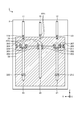
- FIG. 1 is a perspective view showing an example of a schematic configuration of an antenna device according to an embodiment.
- the antenna device 1 shown in FIG. 1 includes a substrate 2, an antenna 10, a parasitic element 11, a parasitic element 12, an antenna 20, a parasitic element 21, a parasitic element 22, and a main plate 30.
- the main plate 30 is shown by hatching.
- XYZ coordinates are shown.
- the Z-axis direction corresponds to the vertical direction
- the X-axis direction and the Y-axis direction correspond to the horizontal direction.
- the substrate 2 is a flat substrate.
- the substrate 2 has a thickness in the X-axis direction, and has a front surface (a surface on the negative direction side of the X-axis) and a back surface (a surface on the positive direction side of the X-axis) extending in the Y-axis direction and the Z direction.
- the term “on the substrate 2” means on the surface of the substrate 2.
- the substrate 2 is, for example, a dielectric substrate having an insulating property.
- the antenna 10 is a first antenna provided on the substrate 2 so as to radiate the first polarized wave.
- the first polarized wave is either a vertically polarized wave or a horizontally polarized wave.
- Vertically polarized waves are electromagnetic waves in which the electric field component in the vertical direction is dominant.
- Horizontally polarized waves are electromagnetic waves in which the electric field component in the horizontal direction is dominant.
- the antenna 10 illustrated in FIG. 1 has a linear shape (rod-shaped) provided on the substrate 2 so as to extend in the positive direction of the Z axis from the base end portion (the portion on the divided main plate 31 side) toward the tip end portion. ) It is a conductive member (for example, a metal pattern).
- the antenna 10 may be a rod-shaped monopole antenna that radiates vertically polarized waves.
- the wavelength of a specific frequency (for example, the center frequency) in the transmission / reception band of the antenna 10 is the wavelength ⁇ 1
- the length of the antenna 10 is set to , for example, 0.25 ⁇ 1.
- the parasitic element 11 and the parasitic element 12 are a pair of parasitic elements provided so as to affect the directivity of the antenna 10.
- the parasitic element 11 and the parasitic element 12 are rod-shaped conductive provided on the substrate 2 so as to extend in the positive direction of the Z axis from the base end portion (the portion on the divided main plate 31 side) toward the tip end portion. It is a sex member.
- the parasitic element 11 and the parasitic element 12 are provided on both sides of the antenna 10 so as to face the antenna 10.
- the parasitic element 11 and the parasitic element 12 are arranged at intervals of, for example, 0.25 ⁇ 1 from the antenna 10.
- the antenna 20 is a second antenna provided on the substrate 2 so as to radiate the second polarized wave.
- the second polarized wave may be polarized wave in the same direction as the first polarized wave radiated by the antenna 10, or may be polarized wave in a direction different from the first polarized wave.
- the antenna 20 illustrated in FIG. 1 is provided on the substrate 2 so as to extend in the negative direction of the Z axis from the base end portion (the portion near the boundary between the split base plate 31 side and the split base plate 32) toward the tip end portion. It is a rod-shaped slot line.
- the antenna 20 is a slot antenna that radiates horizontally polarized waves.
- the antenna 20 is provided so as to be located on the opposite side of the divided main plate 31 from the antenna 10 in the Z-axis direction.
- the wavelength of a specific frequency (for example, the center frequency) in the transmission / reception band of the antenna 20 is the wavelength ⁇ 2
- the length of the antenna 20 is set to , for example, 0.5 ⁇ 2.
- the parasitic element 21 and the parasitic element 22 are a pair of parasitic elements provided so as to affect the directivity of the antenna 20.
- the parasitic element 11 and the parasitic element 22 are rod-shaped slots provided on the substrate 2 so as to extend in the negative direction of the Z axis from the base end portion (the portion on the divided base plate 31 side) toward the tip end portion. It is a railroad track.
- the parasitic element 21 and the parasitic element 22 are provided on both sides of the antenna 20 so as to face the antenna 20.
- the parasitic element 21 and the parasitic element 22 are arranged at intervals of, for example, 0.25 ⁇ 2 from the antenna 20.
- the main plate 30 is a main plate that affects the directivity of the antenna 10 and the antenna 20.
- the main plate 30 includes the divided main plate 31 and the divided main plate 32.
- the divided main plate 31 is a conductive member provided on the substrate 2 so as to affect the directivity of the antenna 10 and / or the antenna 20.
- the divided main plate 31 has a substantially rectangular shape except for a portion where the antenna 20, the parasitic element 21, and the parasitic element 22 are provided.
- the divided base plate 31 is provided so as to face the antenna 10, the parasitic element 11, and the parasitic element 12 in the Z-axis direction.
- the split base plate 31 has a length (length in the Z-axis direction) capable of forming a part of the antenna 20, the parasitic elements 21 and 22 (a portion other than the portion formed by the split base plate 32 described later). Has).
- the divided main plate 32 is a conductive member provided on the substrate 2 so as to affect the directivity of the antenna 10 and / or the antenna 20.
- the divided base plate 32 has a substantially rectangular shape except for a portion where the antenna 20, the parasitic element 21, and the parasitic element 22 are provided.
- the divided main plate 32 is provided so as to face the divided main plate 31 so as to be located on the side opposite to the antenna 10, the parasitic element 11, and the parasitic element 12 with the divided main plate 31 sandwiched in the Z-axis direction.
- the divided base plate 32 may have the same width (length in the Y-axis direction) as the divided base plate 31. Further, the divided base plate 32 has a length (length in the Z-axis direction) capable of forming the antenna 20, the parasitic element 21, and the parasitic element 22.
- the antenna device 1 is provided with a switch group including a plurality of switches. This will be described next with reference to FIG.
- FIG. 2 is a plan view showing a schematic configuration of the antenna device 1.
- a feeding point FP1, a feeding point FP2, and a switch group are shown.
- the switch group includes a switch 111, a switch 121, a switch 211, a switch 212, a switch 221 and a switch 222, and switches 301 to 308.
- the feeding point FP1 is provided on the substrate portion of the antenna 10 and the divided main plate 31.
- the feeding point FP2 is provided at the base end portion of the antenna 20. Alternatively, it is provided at an arbitrary position along the Z axis of the antenna 20.
- the switch 111 is connected to the parasitic element 11.
- the switch 111 is connected between the base end portion of the parasitic element 11 and the divided base plate 31.
- the switch 111 is SHORT (ON: short circuit)
- the parasitic element 11 is connected to the divided main plate 31.
- the switch 111 is OPEN (OFF)
- the parasitic element 11 is separated from the divided main plate 31.
- the switch 121 is connected to the parasitic element 12.
- the switch 121 is connected between the proximal end of the parasitic element 12 and the split base plate 31.
- the switch 121 is SHORT, the parasitic element 12 is connected to the divided main plate 31.
- the switch 121 is OPEN, the parasitic element 12 is separated from the split base plate 31.
- the switch 211 and the switch 212 are connected to the parasitic element 21.
- the switch 211 is connected between the divided main plates 32 on both sides at the base end portion of the parasitic element 21.
- the switch 211 is SHORT
- the parasitic element 21 becomes a slot line having a length from the base end portion to the switch 211.
- the switch 212 is connected between the divided main plates 32 on both sides at a portion between the base end portion and the tip end portion of the parasitic element 21.
- the switch 211 is OPEN and the switch 212 is SHORT, the parasitic element 21 becomes a slot line having a length from the base end portion to the switch 212. In other words, the slot line from the switch 212 to the tip is invalidated.
- the switch 221 and the switch 222 are connected to the parasitic element 22.
- the switch 221 is connected between the divided main plates 32 on both sides at the base end portion of the parasitic element 22.
- the switch 221 is SHORT
- the parasitic element 21 becomes a slot line having a length from the proximal end to the switch 221.
- the switch 222 is connected between the divided main plates 32 on both sides in the portion between the base end portion and the tip end portion of the parasitic element 22.
- the switch 221 is OPEN and the switch 222 is SHORT
- the parasitic element 22 becomes a slot line having a length from the base end portion to the switch 222. In other words, the slot line from the switch 222 to the tip is invalidated.
- Switch 301 to switch 308 are connected to the main plate 30.
- the switches 301 to 308 are connected in order between the divided base plate 31 and the divided base plate 32 in the Y-axis direction.
- the switch 301 is connected between the split base plate 31 and the split base plate 32 at the ends of the split base plate 31 and the split base plate 32 on the positive direction side of the Y axis.
- the switch 302 is connected between the split base plate 31 and the split base plate 32 at a portion of the base end portion of the parasitic element 22 on the positive direction side of the Y axis.
- the switch 303 is connected between the split base plate 31 and the split base plate 32 at a portion of the base end portion of the parasitic element 22 on the negative direction side of the Y axis.
- the switch 304 is connected between the split base plate 31 and the split base plate 32 at a portion of the base end portion of the antenna 20 on the positive direction side of the Y axis.
- the switch 305 is connected between the split base plate 31 and the split base plate 32 at a portion of the base end portion of the antenna 20 on the negative direction side of the Y axis.
- the switch 306 is connected between the split base plate 31 and the split base plate 32 at a portion of the base end portion of the parasitic element 21 on the positive direction side of the Y axis.
- the switch 307 is connected between the split base plate 31 and the split base plate 32 at a portion of the base end portion of the parasitic element 21 on the negative direction side of the Y axis.
- the switch 308 is connected between the divided base plate 31 and the divided base plate 32 at the ends of the divided base plate 31 and the divided base plate 32 on the negative direction side of the Y axis.
- a part of the antenna 20 may be formed of the divided main plate 31, and in this case, the switch 304 and the switch 305 are formed of the portion formed by the divided main plate 31 of the antenna 20 and the divided main plate 32. Connect with the part.
- a part of the parasitic element 21 may be formed of the divided base plate 31, and in this case, the switch 306 and the switch 307 connect the portion of the parasitic element 21 formed of the divided base plate 31 and the portion formed of the divided base plate 32.
- a part of the parasitic element 22 may be formed of the divided base plate 31, and in this case, the switch 302 and the switch 303 connect the portion of the parasitic element 22 formed of the divided base plate 31 and the portion formed of the divided base plate 32. do.
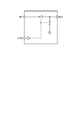
- FIG. 3 is a diagram showing an example of a schematic configuration of SPST.
- the OPEN / SHORT between the terminal RF1 and the terminal RF2 is switched. Switching is controlled by the control signal CTRL. It is also possible to switch so that the terminal RF2 is connected to the ground.
- Example of power feeding method An example of a power feeding method using the power feeding point FP1 and the feeding point FP2 will be described with reference to FIGS. 4A to 4C.
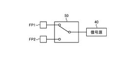
- the power supply system shown in FIG. 4A is an example of a switching diversity scheme.
- the signal source 40 produces a transmit RF signal.
- the transmitted RF signal generated by the signal source 40 is selectively supplied to either the feeding point FP1 or the feeding point FP2 via the switch 50.
- the switch 50 for example, SPDT (Single Pole Double Through) may be used.
- FIG. 5 is a diagram showing an example of a schematic configuration of SPDT. In the SPDT illustrated in FIG.
- the DRIVER switches between the OPEN / SHORT between the terminal RFC and the terminal RF1 and the OPEN / SHORT between the terminal RFC and the terminal RF2 according to the control signal CTRL.
- the DRIVER operates according to the power supply voltage VSS and the power supply voltage VDD. Similarly, it can be a switching diversity in reception.
- the power supply system shown in FIG. 4B is an example of a synthetic diversity scheme.
- the transmission RF signal generated by the signal source 40 is supplied to the feeding point FP1 after being phase-shifted by phase ⁇ 1 by the phase shifter 61, and is supplied to the feeding point FP2 after being phase-shifted by phase ⁇ 2 by the phase shifter 62.
- the antenna 10 and the antenna 20 radiate polarized waves orthogonal to each other, a radiation pattern in which polarization and directivity are combined can be formed.
- it can be a synthetic diversity in reception.
- the power supply method shown in FIG. 4C is an example of MIMO (Multiple Input Multiple Output).
- the signal source 41 and the signal source 42 generate different transmission RF signals.
- the transmission RF signal generated by the signal source 41 is supplied to the feeding point FP1.
- the transmitted RF signal generated by the signal source 42 is supplied to the feeding point FP2.
- MIMO with low correlation and high S / N is realized. Similarly, it can be MIMO in reception.
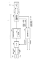
- FIG. 6 is a diagram showing an example of a schematic configuration of an antenna device and an electronic device constituting such a control system.
- the antenna device 1 includes an RF signal processing block 400, a switching control block 500, and a modulation / demodulation signal processing block 600 in addition to the configurations described so far.
- the antenna device 1 is mounted on the electronic device 5, and a portion of the electronic device 5 other than the antenna device 1 is shown as another block 700.
- the power feeding scheme is a switching diversity scheme (FIG. 4A).
- the other block 700 is configured to supply transmission data to the modulation / demodulation signal processing block 600 of the antenna device 1 and to receive received data from the modulation / demodulation signal processing block 600.
- the modulation / demodulation signal processing block 600 generates a modulated signal based on the transmitted data.
- the RF signal processing block 400 generates a transmit RF signal based on the modulated signal.
- the generated transmission RF signal is supplied to the feeding point FP1 or the feeding point FP2 (FIG. 2) of the antenna device 1 via the switch 50.
- the received RF signal is supplied from the antenna device 1 to the RF signal processing block 400 via the switch 50.
- the RF signal processing block 400 processes the received RF signal (amplification, filtering, frequency conversion, etc.).
- the modulation / demodulation signal processing block 600 demodulates the processed received RF signal to obtain received data.
- an index related to transmission / reception is sent to the switching control block 500.
- indicators are reception level information (RSSI: Received Signal Strength Indicator), transmission level information, reception QoS (Quality of Service) information (SIR: signal-to-interference ratio, BER: Bit Error Rate), and transmission QoS information. Yes, but not limited to these.
- the changeover control block 500 generates a changeover signal for controlling each of the switch 50, the switch 111, the switch 121, the switch 211, the switch 212, the switch 221, the switch 222, the switch 301 to the switch 308 (FIG. 2), and the switch 50. do.
- the switching signal is generated based on the above-mentioned index sent from the modulation / demodulation signal processing block 600.
- the switching control block 500 generates a switching signal so that at least one index of each of the above-mentioned indexes is maximized.
- the antenna device 1 has various states as described below due to the switching control by the switching control block 500.
- FIG. 7 is a diagram showing an example of State.
- FIG. 7 shows 24 types of States from State 00 to State 23. “ON” means that power is supplied to the antenna by the corresponding feeding point, and “OFF” means that power is not supplied. “OPEN” means that the corresponding switch is in a non-conducting state (open), and “SHORT” means that it is in a conductive state (short circuit).
- States00 to State05 are examples in which power is supplied (excited) only to the antenna 10 and the switches connected to the parasitic element 11, the parasitic element 12, the divided base plate 31 and the divided base plate 32 are switched.
- States 06 to 08 are examples in which power is supplied only to the antenna 20 and the switch connected to the parasitic element 21 and the parasitic element 22 is switched.
- the State 09 and the State 10 are examples in which power is supplied only to the antenna 10 and the switches connected to the parasitic element 21, the parasitic element 22, the divided base plate 31 and the divided base plate 32 are switched.
- States 11 to 23 are examples in which power is supplied only to the antenna 20 and switches connected to the parasitic element 11, the parasitic element 12, the parasitic element 21, and the parasitic element 22 are switched.
- State00 to State23 various States can be obtained.
- Examples include a State that switches each one independently.
- Lengths of the parasitic element 11 in the Y and Z axis directions 10 mm and 80 mm, respectively.
- Lengths of the parasitic element 12 in the Y and Z axis directions 10 mm and 80 mm, respectively.
- Distance between the antenna 10 and the parasitic element 11 in the Y-axis direction 75 mm.
- Distance between the antenna 10 and the parasitic element 12 in the Y-axis direction 75 mm.
- Lengths of antenna 20 in the Y and Z axis directions (of slots) 10 mm and 170 m, respectively.
- Lengths of the parasitic element 21 in the Y and Z axis directions 10 mm and 190 m, respectively.
- Lengths of the parasitic element 22 in the Y and Z axis directions 10 mm and 190 m, respectively.
- Distance between switch 222 and switch 222 in the Z-axis direction 5 mm.
- Distance between the antenna 20 and the parasitic element 21 in the Y-axis direction 75 mm.
- Distance between the antenna 20 and the parasitic element 22 in the Y-axis direction 75 mm.
- Lengths of the divided base plate 31 in the Y and Z axis directions 250 mm and 45 mm, respectively.
- Lengths of the divided base plate 32 in the Y and Z axis directions 250 mm and 200 mm, respectively.
- Distance between the divided base plate 31 and the divided base plate 32 in the Z-axis direction 5 mm.
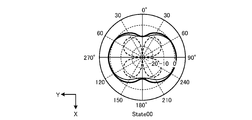
- FIGS. 8A to 8C show the simulation results of State00 to State02.
- the solid line shows the gain of vertically polarized waves (dBi)
- the broken line shows the gain of horizontally polarized waves
- the thick solid line shows the total gain (dBi).
- the radiation of vertically polarized waves in the Y-axis direction is dominant. This is because the antenna 10, the parasitic element 11, and the parasitic element 12, which are conductive members, are provided side by side in the Y-axis direction.
- State02 (FIG. 8C) has a larger gain in the positive direction of the Y-axis than State00 (FIG. 8A). This is because, of the parasitic element 11 and the parasitic element 12, only the parasitic element 12 is connected to the divided main plate 31 by the switch 121, so that the parasitic element 12 operates as a reflecting element.
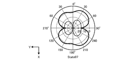
- FIGS. 9A to 9C show the simulation results of State06 to State08.
- the solid line shows the gain of vertically polarized waves (dBi)
- the broken line shows the gain of horizontally polarized waves
- the thick solid line shows the total gain (dBi).
- the radiation of horizontally polarized waves in the X-axis direction is dominant. This is because the antenna 20, the parasitic element 21, and the parasitic element 22, which are slot lines, are provided side by side in the Y-axis direction.
- the State 00 to State 02 and the State 06 to State 08 described above are directional by switching the polarization by switching between the antenna 10 and the antenna 20, and by switching the switch 111, the switch 121, the switch 211, the switch 212, the switch 221 and the switch 222. This is an example of control. In addition to this, those skilled in the art can understand that the directivity is also controlled by switching the switch 301 to the switch 308.
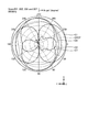
- FIG. 10 shows a contrast between State 01 and State 03.
- the solid line shows the total gain (dBi) of State 1
- the broken line shows the total gain (dBi) of State 03.
- the State 03 realizes a directivity different from that of the State 01. This is because in State 03, the current flowing through the main plate 30 and the divided main plate 31 changes because the divided main plate 31 and the divided main plate 32 are connected by the switches 301 to 308 and the pattern of the main plate 30 is changed. ..
- the antenna device 1 can have various States having different polarization and directivity.
- the State of the antenna device 1 is controlled by the switching control block 500 described above with reference to FIG.
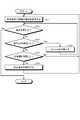
- FIG. 11 is a flowchart showing an example of switching control processing (control method of the antenna device 1). This process is repeatedly executed by the switching control block 500, for example, while transmission / reception (use of the electronic device 5) by the antenna device 1 is being performed.
- step S1 the switching control block 500 acquires an index related to transmission / reception. For example, as described above with reference to FIG. 6, indexes such as reception level information (RSSI), transmission level information, reception QoS information (SIR, BER), and transmission QoS information are acquired.
- RSSI reception level information
- SIR transmission level information
- BER reception QoS information
- transmission QoS information transmission QoS information
- step S2 the switching control block 500 determines whether or not a predetermined condition is satisfied. For example, when searching for a State in which the best index can be obtained, it is determined that a predetermined condition is satisfied when the index acquired in the previous step S1 is better than the index acquired in step S1 of the previous loop. You can do it. Alternatively, if a State that satisfies a certain index is sufficient, it may be determined that the predetermined condition is satisfied when the index acquired in the previous step S1 exceeds the threshold value. In addition to this, various conditions may be used as predetermined conditions. When the predetermined condition is satisfied (Yes in step S2), the processing of the flowchart ends. If the predetermined condition is not satisfied (No in step S2), the process is returned to step S1 again via step S3.
- step S3 the changeover control block 500 switches the switch. Which switch is to be switched may be appropriately determined. For example, each switch may be switched so that State 00 to State 23 described above are sequentially realized each time steps S1 to S3 are looped.
- the antenna device 1 can be switched to the State where the desired directivity can be obtained.
- FIG. 12 is a plan view showing a schematic configuration of an antenna device according to such a modification.
- the antenna device 1A shown in FIG. 12 is different from the antenna device 1 (FIG. 2) in that the position of the feeding point of the antenna 20 is different.
- the two feeding points FP2A1 and the feeding point FP2A2 are provided at arbitrary positions of the antenna 20.
- the number and position of the feeding point FP2A1 and the feeding point FP2A2 are examples, and various other feeding points may be provided at various positions.
- FIG. 13 is a plan view showing a schematic configuration of an antenna device according to such a modification.
- the antenna device 1B shown in FIG. 13 is different from the antenna device 1 (FIG. 2) in that the split base plate 32B is provided instead of the split base plate 32 and that the switches 309 to 316 are provided.
- the divided base plate 32B is divided into five parts: a first part 321, a second part 322, a third part 323, a fourth part 324, and a fifth part 325. Each part is connected by switches 309 to 316.
- the first portion 321 and the second portion 322 are provided between the antenna 20 and the parasitic element 21 in order from the base end portion to the tip end portion of the antenna 20 (in the negative direction of the Z axis).
- the first portion 321 and the second portion 322 have a substantially rectangular shape.
- the switch 309 is connected between the first portion 321 and the second portion 322 in the vicinity of the parasitic element 21.
- the switch 310 is connected between the first portion 321 and the second portion 322 in the vicinity of the antenna 20.
- the third portion 323 and the fourth portion 324 are sequentially provided between the antenna 20 and the parasitic element 22 in the direction from the base end portion to the tip end portion of the antenna 20.
- the third portion 323 and the fourth portion 324 have a substantially rectangular shape.
- the switch 311 is connected between the third portion 323 and the fourth portion 324 in the vicinity of the antenna 20.
- the switch 312 is connected between the third portion 323 and the fourth portion 324 in the vicinity of the parasitic element 22.
- the fifth portion 325 is a portion of the divided base plate 32 other than the first portion 321 to the fourth portion 324.
- the portion provided between the antenna 20 and the parasitic element 21 is connected to the second portion 322 via the switch 313 and the switch 314.
- the switch 313 is connected between the second portion 322 and the fifth portion 325 in the vicinity of the parasitic element 21.
- the switch 314 is connected between the second portion 322 and the fifth portion 325 in the vicinity of the antenna 20.
- the portion provided between the antenna 20 and the parasitic element 22 is connected to the fourth portion 324 via the switch 315 and the switch 316.
- the switch 315 is connected between the fourth portion 324 and the fifth portion 325 in the vicinity of the parasitic element 22.
- the switch 316 is connected between the fourth portion 324 and the fifth portion 325 in the vicinity of the parasitic element 22.
- the switch 309 to 316 are switched by the changeover control block 500 (FIG. 6). By switching the switch 309 to 316, the pattern of the divided base plate 32B is changed, thereby obtaining different directivity.
- the division pattern and connection relationship of the division base plate 32B are not limited to the example shown in FIG.
- FIG. 14 is a plan view showing a schematic configuration of an antenna device according to such a modification.
- the antenna device 1C shown in FIG. 14 has a parasite 10, a parasitic element 11, a parasitic element 12, an antenna 20, a parasitic element 21, a parasitic element 22, a switch 212, and a switch 222, as compared with the antenna device 1 (FIG. 2).
- the antenna 10C is different from the antenna 10 (FIG. 2) in that the switch 101 and the feeding point FP1C0 are provided at the base end portion.
- the switch 101 is provided in parallel with the feeding point FP1C0.
- the switch 101 is switched by the switching control block 500 (FIG. 6). By setting the switch 101 to SHORT, the antenna 10C can be used as a parasitic element instead of exciting the antenna 10C via the feeding point FP1C0.
- the parasitic element 11C is different from the parasitic element 11 (FIG. 2) in that a feeding point FP1C1 is provided at the base end portion.
- the switch 111 is provided in parallel with the feeding point FP1C1. By setting the switch 111 to OPEN, the parasitic element 11C can be excited via the feeding point FP1C1 and the parasitic element 11C can be used as an antenna.
- the parasitic element 12C is different from the parasitic element 12 (FIG. 2) in that a feeding point FP1C2 is provided at the base end portion.
- the switch 121 is provided in parallel with the feeding point FP1C2. By setting the switch 121 to OPEN, the parasitic element 12C can be excited via the feeding point FP1C2, and the parasitic element 12C can be used as an antenna.
- the antenna 20C is different from the antenna 20 (FIG. 2) in that the feeding point FP2C0 is provided instead of the feeding point FP2.
- the feeding point FP2C0 is not limited to the proximal end portion of the antenna 20, and is provided at an arbitrary position of the antenna 20.
- the switch 201C is connected in parallel with the feeding point FP2C0. That is, the switch 201C is connected between the divided main plates 32 at both ends of the antenna 20C.
- the switch 201C is switched by the switching control block 500 (FIG. 6). By setting the switch 201C to SHORT, the antenna 20C can be used as a parasitic element instead of exciting the antenna 20C via the feeding point FP2C1.
- the parasitic element 21C is different from the parasitic element 21 (FIG. 2) in that the feeding point FP2C1 is provided and that the switch 212C is provided instead of the switch 212.
- the feeding point FP2C1 is provided at an arbitrary position of the parasitic element 21C.
- the switch 212C is connected in parallel with the feeding point FP2C1. That is, the switch 212C is connected between the divided main plates 32 at both ends of the parasitic element 21.
- the switch 212C is switched by the switching control block 500 (FIG. 6).
- the switch 212C is set to OPEN, the parasitic element 21C can be excited via the feeding point FP2C1 and the parasitic element 21C can be used as an antenna.
- the parasitic element 22C is different from the parasitic element 22 (FIG. 2) in that the feeding point FP2C2 is provided and that the switch 222C is provided instead of the switch 222.
- the feeding point FP2C2 is provided at an arbitrary position of the parasitic element 22C.
- the switch 222C is connected in parallel with the feeding point FP2C2. That is, the switch 222C is connected between the divided main plates 32 at both ends of the parasitic element 22C.
- the switch 222C is switched by the switching control block 500 (FIG. 6).
- the switch 222C is set to OPEN, the parasitic element 22C can be excited via the feeding point FP2C2, and the parasitic element 22C can be used as an antenna.
- FIG. 15 is a plan view showing a schematic configuration of an antenna device according to such a modification.
- the antenna device 1D shown in FIG. 15 includes an antenna 10D, a parasitic element 11D, and a parasitic element 12D in place of the antenna 10, the parasitic element 11, and the parasitic element 12. It's different.
- the antenna 10D is different from the antenna 10 (FIG. 2) in that it is a foldable antenna having a foldable portion.
- the antenna 10D has a portion extending in the positive direction of the Z axis from the base end portion, two portions bent from the portion extending in the positive direction of the Y axis and extending in the negative direction of the Y axis, and further from them. It has a portion that is bent and extends in the negative direction of the Z axis.
- the parasitic element 11D includes a portion extending in the Z-axis positive direction from the base end portion, a portion bent from the base end portion extending in the Y-axis positive direction, and a portion further bent from there and extending in the Z-axis negative direction.
- the parasitic element 12D includes a portion extending in the positive direction of the Z axis from the base end portion, a portion bent from there and extending in the negative direction of the Y axis, and a portion bent from there and extending in the negative direction of the Z axis.
- the bent shape of the antenna 10D, the parasitic element 11D, and the parasitic element 12D makes the antenna device 1D more compact than the antenna device 1.
- the shapes of the antenna 10D, the parasitic element 11D, and the parasitic element 12D may be any shape as long as they can shorten the length in the Z-axis direction, and are not limited to the example shown in FIG.
- the antenna 10D may have a curved portion instead of the bent portion, or may have both a bent portion and a curved portion.
- FIG. 16 is a plan view showing a schematic configuration of an antenna device according to such a modification.
- the antenna device 1E shown in FIG. 16 is different from the antenna device 1 (FIG. 2) in that it includes a variable reactance element 111E and a variable reactance element 121E in place of the switch 111 and the switch 121.
- the variable reactance element 111E and the variable reactance element 121E are one aspect of the switches constituting the switch group.
- variable reactance element 111E and the variable reactance element 121E exemplified are capacitors capable of changing the capacitance value such as a varicap.
- the capacitance values of the variable reactance element 111E and the variable reactance element 121E are controlled by the switching control block 500 (FIG. 6).
- Different directivity can also be obtained by changing the reactance values of the variable reactance element 111E and the variable reactance element 121E to switch the connection state between the parasitic element 11 and the divided base plate 31.
- FIG. 17 is a plan view showing a schematic configuration of an antenna device according to such a modification.
- the antenna device 1F shown in FIG. 17 includes a parasitic element 21F and a parasitic element 22F instead of the parasitic element 21 and the parasitic element 22, and the switch 213F and the switch 223F. It differs in that it is provided.
- the switch 213F is provided at an arbitrary position between the switch 211 and the switch 212 on the parasitic element 21F.
- the switch 213F is connected between the divided main plates 32 on both sides of the parasitic element 21F.
- the parasitic element 21 has a line length of the length from the proximal end to the switch 214.
- the switch 223F is provided at an arbitrary position between the switch 221 and the switch 222 on the parasitic element 22F.
- the switch 223F is connected between the divided main plates 32 on both sides of the parasitic element 22.
- the parasitic element 22 has a line length of the length from the proximal end to the switch 224.
- Different directivity can also be obtained by finely switching the lengths of the parasitic element 21F and the parasitic element 22F by the switch 213F and the switch 223F.
- additional switches may be added.
- the radiation pattern can be freely changed with various combinations other than those described above, such as the combination of excitation with vertically polarized waves and parasitic elements with horizontally polarized waves, to further optimize communication performance. can do. It is also possible to make each element multi-band. It is also possible to mount an antenna tuning element to widen the band.
- FIG. 18 is a diagram showing an example of a schematic configuration of an antenna device according to a second embodiment.
- the antenna device 1G shown in FIG. 18 is different from the antenna device 1 (FIG. 2) in that the antenna 20G and the main plate 33 are provided in place of the antenna 20 and the main plate 30.
- the antenna device 1G is shown in a mode that does not have the parasitic element 21 and the parasitic element 22 as in the antenna device 1 (FIG. 2), but has a configuration corresponding to such a parasitic element 21 and the parasitic element 22. You may have it.
- the antenna 20G is a second antenna provided on the substrate 2 so as to radiate the second polarized wave.
- the second polarized wave radiated by the antenna 20G is a polarized wave in the same direction as the first polarized wave radiated by the antenna 10.
- the antenna 20G illustrated in FIG. 18 is a slot antenna provided on the substrate 2 so as to extend in the horizontal direction, and emits vertically polarized waves.
- the feeding point FP2G of the antenna 20G may be provided at an arbitrary position of the antenna 20G.
- the main plate 33 is provided on the substrate 2 so as to have an area (pattern length and pattern width) that can affect the radiation characteristics of the antenna 10 and / or 20G.
- the main plate 33 has a substantially rectangular shape except for a portion where the antenna 20G is provided.
- the main plate 33 has a length (length in the Y-axis direction) capable of forming the antenna 20G.
- the antenna 20G is excited via the feeding point FP2G.
- the antenna device 1G also has various States as described below by the switching control block 500 (FIG. 6).
- FIG. 19 is a diagram showing an example of State.
- Beam orientation indicates the direction of directivity.
- Y- corresponds to the negative direction of the Y axis.
- Y + corresponds to the positive direction of the Y axis.
- X ⁇ corresponds to the positive direction of the X axis and the negative direction of the X axis.
- eight types of Stages 200 to 207 can be obtained.
- Lengths of the parasitic element 11 in the Y and Z axis directions 2 mm and 67 mm, respectively.
- Lengths of the parasitic element 12 in the Y and Z axis directions 2 mm and 67 mm, respectively.
- Distance between the antenna 10 and the parasitic element 11 in the Y-axis direction 88 mm.
- Distance between the antenna 10 and the parasitic element 12 in the Y-axis direction 88 mm.
- Lengths (of slots) of antenna 20 in the Y and Z axes, respectively 200 and 4 mm.
- Distance from one end of the antenna 20 in the Y-axis direction to the feeding point FP2G 60 mm.
- Lengths of the main plate 33 in the Y and Z axis directions 209 mm and 150 mm, respectively.
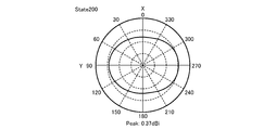
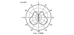
- 20A to 20E show the simulation results of State200.
- 20A to 20C show the directivity when viewed in the XY plane, the XZ plane, and the YZ plane.
- directivity is obtained especially in the Y-axis direction. This is because the antenna 10, the parasitic element 11, and the parasitic element 12, which are conductive members, are provided side by side in the Y-axis direction. Further, almost symmetrical directivity can be obtained in the X-axis direction and the Y-axis direction. This is because the parasitic element 11 and the parasitic element 12 are both separated from the main plate 33 by the switch 111 and the switch 121, and the influence of the parasitic element 11 and the parasitic element 12 on the antenna 10 is small.
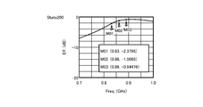
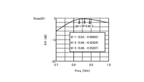
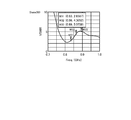
- FIG. 20D shows the radiation efficiency (dB) and FIG. 20E shows VSWR.
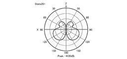
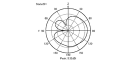
- FIGS. 21A to 21E show the simulation results of State201.
- the gain in the negative direction of the Y axis is larger in the State 201 than in the State 200 (FIGS. 20A to 20C).
- the parasitic element 11 and the parasitic element 12 only the parasitic element 11 is connected to the main plate 33 by the switch 111, so that the parasitic element 11 operates as a reflecting element.
- markers M11 to M13 in FIGS. 21D and 21E good radiation efficiency and VSWR are still obtained at frequencies of 0.83 GHz to 0.89 GHz.
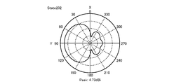
- FIGS. 22A to 22E show the simulation results of State202.
- the gain in the positive direction of the Y-axis is larger in the State 202 than in the State 200 (FIGS. 20A to 20C).
- the parasitic element 11 and the parasitic element 12 only the parasitic element 12 is connected to the main plate 33 by the switch 121, so that the parasitic element 12 operates as a reflecting element.
- markers M21 to M23 in FIGS. 22D and 22E good radiation efficiency and VSWR are still obtained at frequencies of 0.83 GHz to 0.89 GHz.
- FIGS. 23A to 23E show the simulation results of State 203.
- the gains in the X-axis direction and the Y-axis positive direction change as compared with the State 200 (FIGS. 20A to 20C). It is considered that this is because the parasitic element 11 and the parasitic element 12 are connected to the main plate 33 by the switch 111 and the switch 121, so that the influence of the parasitic element 11 and the parasitic element 12 on the antenna 10 is changed.
- markers M31 to M33 in FIGS. 23D and 23E changes also occur in radiation efficiency and VSWR at frequencies of 0.83 GHz to 0.89 GHz.
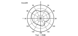
- FIGS. 24A to 24E show the simulation results of State204.
- State 204 directivity is obtained particularly in the X-axis direction. This is because the antenna 20G, which is a slot line, is provided in the Y-axis direction. Further, almost symmetrical directivity can be obtained in the X-axis direction and the Y-axis direction. This is because the main plate 33 is separated from the parasitic element 11 and the parasitic element 12 by the switch 111 and the switch 121, and the influence of the parasitic element 11 and the parasitic element 12 on the antenna 20G is small. As shown by markers M41 to M43, good radiation efficiency and VSWR are still obtained at frequencies of 0.83 GHz to 0.89 GHz.
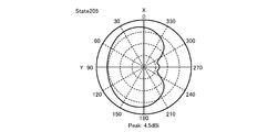
- 25A to 25E show the simulation results of State 205.
- the gain in the positive direction of the Y-axis is larger in the State 205 than in the State 204 (FIGS. 24A to 24C). It is considered that this is because the main plate 33 is connected to the parasitic element 11 by the switch 111, and the influence of the parasitic element 11 on the antenna 20G has changed.
- markers M51 to M53 good radiation efficiency and VSWR are still obtained at frequencies of 0.83 GHz to 0.89 GHz.
- FIGS. 26A to 26E show the simulation results of State 206.
- the gain in the X-axis direction and the Y-axis direction changes in the State 206 as compared with the State 204 (FIGS. 24A to 24C). It is considered that this is because the main plate 33 is connected to the parasitic element 12 by the switch 121, and the influence of the parasitic element 12 on the antenna 20G has changed.
- markers M61 to M63 good radiation efficiency and VSWR are still obtained at frequencies of 0.83 GHz to 0.89 GHz.
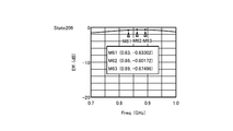
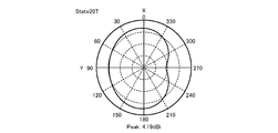
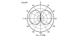
- FIGS. 27A to 27E show the simulation results of State 207.
- the gain in the positive direction of the Y axis is larger than that in State 204 (FIGS. 24A to 24C). It is considered that this is because the main plate 33 is connected to the parasitic element 11 and the parasitic element 12 by the switch 111 and the switch 121, so that the influence of the parasitic element 11 and the parasitic element 12 on the antenna 20G is changed.
- markers M71 to M73 good radiation efficiency and VSWR are still obtained at frequencies of 0.83 GHz to 0.89 GHz.
- FIG. 28 shows a contrast between State 200 to State 207.
- Curves C0 to C7 show the gains of State 200 to State 207.
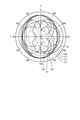
- a gain of ⁇ 5 dBi can be obtained in all directions of 360 degrees by switching between State 200 to State 207.
- FIG. 29 is a diagram showing a prototype. As shown in FIG. 29, in the prototype, the antenna 10 was excited from the port PORT1 via the transmission line LINE1 (and the feeding point FP1). The antenna 20G was excited from the port PORT2 via the transmission line LINE2 (feeding point FP2).
- the transmission line LINE1 and the transmission line LINE2 are microstrip lines in this example. However, in addition to the microstrip line, a coplanar line, a strip line, or the like may be used. Since the substrate 2, the antenna 10, the antenna 20G, and the main plate 33 are the same as the above simulation conditions, the description will not be repeated here.
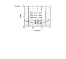
- FIG. 30A shows the experimental results of State 201.
- the solid line shows the directivity at a frequency of 830 MHz.
- the thick solid line indicates the directivity at a frequency of 860 MHz.
- the broken line indicates the directivity at a frequency of 890 MHz.
- FIG. 30B shows the experimental results of State202. Experimental results close to the simulation results described above with reference to FIG. 22A and the like were obtained.
- FIG. 30C shows the experimental results of State204. Experimental results close to the simulation results described above with reference to FIG. 24A and the like were obtained.
- FIG. 31 shows the experimental results of State201, State202, State206 and State207.
- Curve C1, curve C2, curve C6 and curve C7 show the directivity of State201, State202, State206 and State207.
- the curved CREF indicates the directivity of a commercially available sleeve dipole antenna (almost omnidirectional antenna). For example, when viewed on the XY plane, it was confirmed that a gain of ⁇ 5 dBi can be obtained in all directions of 360 degrees by switching State201, State202, State206, and State207.
- FIG. 32 is a plan view showing a schematic configuration of an antenna device according to such a modification.
- the antenna device 1H shown in FIG. 32 is different from the antenna device 1G (FIG. 18) in that it includes an antenna 10H1 and an antenna 10H2 instead of the antenna 10 and a hybrid element 90.
- Both the antenna 10H1 and the antenna 10H2 are monopole antennas extending in the positive direction of the Z axis.
- the hybrid element 90 is a 90-degree hybrid element, and distributes signals from the feeding point FP1H to supply signals having different phases of 90 ° to the antenna 10H1 and the antenna 10H2, respectively.
- the antenna 10 may be excited in the first frequency band (eg 800 MHz band) and the antenna 20 may be excited in the second frequency band (eg 2 GHz band).
- the signal in the first frequency band is radiated by the antenna 10 with directivity in the Y-axis direction.
- the signal in the second frequency band is radiated by the antenna 20 with directivity in the X-axis direction. Therefore, the antenna device 1H functions as a direct beam antenna in which the directivity of different frequency bands constituting the multi-band is orthogonal. Further, by using a pair of antennas, the antenna device 1H can be made smaller than the configuration having two elements of the parasitic element 11 and the parasitic element 12.
- FIG. 33 is a plan view showing a schematic configuration of an antenna device according to such a modification.
- the antenna device 1J shown in FIG. 33 includes an antenna 10J1 and an antenna 10J2 instead of the antenna 10H1 and the antenna 10H2, and a switch 101J1 and a switch 101J2.
- the difference is that the hybrid element 90 is not provided.
- the switch 101J1 is a SPDT switch connected between the antenna 10J1, the main plate 33, and the switch 101J3.
- the switch 101J1 switches between a state in which the antenna 10J1 is connected to the main plate 33 and a state in which the antenna 10J1 is connected to the switch 101J3.
- the switch 101J1 is switched by the switching control block 500 (FIG. 6).
- the switch 101J2 is a SPDT switch connected between the antenna 10J2, the main plate 33, and the switch 101J3.
- the switch 101J2 switches between a state in which the antenna 10J2 is connected to the main plate 33 and a state in which the antenna 10J2 is connected to the switch 101J3.
- the switch 101J2 is switched by the switching control block 500 (FIG. 6).
- the switch 101J3 is a SPDT switch connected between the switch 101J2, the switch 101J2, and the signal source 40 (see FIG. 4A and the like).
- the switch 101J3 switches between a state in which the switch 101J1 is connected to the signal source 40 (excited state) and a state in which the switch 101J2 is connected to the signal source 40 (excited state).
- the use of the antenna 10J1 and the antenna 10J2 can be switched between the antenna and the parasitic element.
- the antenna device 1J can be made smaller than the configuration having two elements, the parasitic element 11 and the parasitic element 12.
- the antenna device 1G according to the second embodiment can be modified in the same manner as the antenna device 1 according to the first embodiment.
- the parasitic element 21 and the parasitic element 22 for the antenna 20 as described above with reference to FIG. 2 may be provided for the antenna 20G of the antenna device 1G.
- These parasitic elements may be provided so as to extend along the extending direction (Y-axis direction) of the antenna 20G.
- the modification described above with reference to FIGS. 11 to 17 may be applied to the substrate 2G.
- FIG. 34 is a plan view showing an example of a schematic configuration of an antenna device according to such a modified example.
- the antenna device 1K shown in FIG. 34 includes an antenna 20K, a parasitic element 21K, a parasitic element 22K, an antenna 23K, a parasitic element 24K, and a parasitic element 25K as slot lines formed by the main plate 34.
- the antenna 20K is a slot antenna extending in the Z-axis direction, and is excited via the feeding point FP2.
- the parasitic element 21K and the parasitic element 22K are provided on both sides of the antenna 20K.
- the antenna 23K is a slot antenna extending in the Y-axis direction, and is excited via the feeding point FP3K.
- the parasitic element 24K and the parasitic element 25K are provided on both sides of the antenna 23K.
- the feeding point FP2K is arranged at an arbitrary position along the antenna 20K, and the feeding point FP3K is arranged at an arbitrary position along the antenna 23K. However, it is desirable to avoid the inside of the parasitic slot.
- the antenna device 1K includes switches 251 to 262 as switches for switching the lengths of the antenna 20K, the parasitic element 21K, the parasitic element 22K, the antenna 23K, the parasitic element 24K, and the parasitic element 25K.
- switches 251 to 262 are provided so as to surround the intersection of the slot lines.
- the arrangement of the switches is not limited to the example of FIG. 34.
- the antenna device 1K also has various States as described below by the switching control block 500 (FIG. 6).
- FIG. 35 is a diagram showing an example of State. “V” indicates vertically polarized waves, and “H” indicates horizontally polarized waves. As shown in FIG. 35, the States 300 to 308 in which the polarization and the directivity are switched can be obtained. Not limited to the example shown in FIG. 35, various states can be obtained by individually switching each feeding point and switch.
- the components of the antenna device 1 such as the antenna, the parasitic element, the main plate, and the switch group are provided on the surface of the substrate 2 has been described.
- a part or all of the components of the antenna device 1 may be provided on the back surface of the substrate 2.
- the frequency band of the antenna device according to the embodiment is not limited to the 800 MHz and 2 GHz bands. Examples of other frequency bands are the 2.4 GHz band, the 5 GHz band, and even the millimeter wave band, which is a higher frequency band.
- the antenna device according to the embodiment may be applied to radio waves in any frequency band including these.
- Antenna devices may be applied to any wireless system that utilizes those frequency bands. Examples of wireless systems are LTE (Long Term Evolution), UWB (Ultra Wide Band), WiFi (registered trademark), and the like.
- Antenna devices can be applied to any application that utilizes those frequency bands or wireless systems. Examples of applications are telephone calls, data communications, distance measurement, positioning, motion sensing, and the like.
- each switch or the like is set based on indexes such as reception level information (RSSI), transmission level information, reception QoS information (SIR, BER), and transmission QoS information.
- RSSI reception level information
- SIR reception QoS information
- BER reception QoS information
- transmission QoS information transmission QoS information
- the transmission level information may include transmission power and the like.
- the received QoS information may include an indicator included in the packet and the like. The same applies to the transmitted QoS information.
- Many wireless transmission / reception signals include an indicator indicating the quality of the signal in the packet.
- An example of an indicator is a numerical value determined according to the level of quality. Examples of numerical values are numerical value 1 indicating that the quality is good (Good Quality), numerical value 2 indicating that the quality is low (Low Quality), and unreliable (for any) that the reliability is low due to some reason such as loss of a signal. Reason like Signal Lost, etc)), and a numerical value 4 indicating that the quality is unknown (Unknown quality).
- the information regarding the frequency characteristics includes the information regarding the frequency characteristics of the received signal and the frequency characteristics of the transmitted signal.
- Examples of information regarding the frequency characteristics of the received signal are the frequency characteristics of the phase or amplitude of the received signal and the information based on the frequency characteristics (gradient value, moving average value, etc.).
- Examples of information regarding the frequency characteristics of the transmission signal are the frequency characteristics of the phase or amplitude of the transmission signal and information based on the frequency characteristics (gradient value, moving average value, etc.).
- the phase or amplitude may be a relative value relative to the phase or amplitude at a certain frequency. Such an index will be described with reference to FIGS. 36A to 36C.
- FIGS. 36A to 36C are diagrams schematically showing an example of information regarding frequency characteristics.
- FIGS. 36A and 36B show examples of phase or amplitude frequency characteristics at different States.
- the horizontal axis of the graph indicates frequency, and the vertical axis indicates phase or amplitude.
- the frequency range is the transmission / reception frequency band of the antenna (for example, 2.4 GHz to 2.48 GHz, etc.).
- the phase or amplitude changes to decrease at a substantially constant rate as the frequency increases.
- FIG. 36B as the frequency increases, the phase or amplitude changes repeatedly and irregularly.
- the frequency characteristics of the phase or amplitude of the transmission signal or the reception signal can also be used as an index.
- control may be performed such as selecting a State whose frequency characteristics satisfy a predetermined condition, selecting a State having the optimum frequency characteristics, and selecting a State having the minimum variation in the frequency characteristics.
- FIG. 36C shows an example of the slope value of the frequency characteristic of the phase or amplitude in each of the different States.
- Graph line A shows the slope value of the frequency characteristic shown in FIG. 36A described above.
- Graph line B shows the slope of the frequency characteristic shown in FIG. 36C described above. Since the slope of the phase or amplitude frequency characteristic differs depending on the State, the slope of the phase or amplitude frequency characteristic can also be used as an index. For example, a State in which the fluctuation of the slope value of the frequency characteristic satisfies a predetermined condition (for example, -30 dB / Hz or less as an initial value) is selected, or a state in which the fluctuation of the slope value of the frequency characteristic is minimized is selected. Control may be performed.
- a predetermined condition for example, -30 dB / Hz or less as an initial value
- the information regarding the time-axis waveform includes information regarding the time-axis waveform of the received signal and information regarding the time-axis waveform of the transmitted signal.
- Examples of information regarding the time-axis waveform of the received signal are the time-axis waveform of the received signal and information based on the time-axis waveform (width of initial peak, amplitude of initial peak, detection time of initial peak, etc.).
- Examples of information regarding the time-axis waveform of the transmission signal are the time-axis waveform of the transmission signal and information based on the time-axis waveform (width of initial peak, amplitude of initial peak, detection time of initial peak, etc.).
- the information on the time axis waveform is useful, for example, when the antenna device 1 is used as a distance measuring and positioning device or the like. Information on the time axis waveform will be described with reference to FIG. 37.
- FIG. 37 is a diagram schematically showing an example of information regarding the time axis waveform.
- the horizontal axis of the graph shows time, and the vertical axis shows the amplitude value (detection value).
- the amplitude value is standardized by the value of the first wave peak.
- the time from the detection of the signal to the peak of the first wave is referred to as time T1 and is shown in the figure.
- the first wave peak is referred to as a width W1 and is shown in the figure.
- Time T1 starts when the amplitude value of the detection signal first exceeds a predetermined level (about 0.05 in this example). In this example, the detection amplitude reaches 0.5 when half of the time T1 elapses from the start of detection.
- the time axis waveform as shown in FIG. 37 may also differ depending on the State. Therefore, the time axis waveform can also be used as an index. For example, control may be performed such that a State whose time axis waveform (time T1, width W1, etc.) satisfies a predetermined condition is selected.
- the initial value of the predetermined condition may be set to, for example, 15 ns or less, 10 ns or less, and a State satisfying this may be selected.
- Control may be performed such as selecting the State having the optimum time axis waveform (time T1, width W1, etc.). For example, the State with the shortest time T1 may be selected. Alternatively, the State having the narrowest width W1 may be selected.
- Confirmation of the index in the above-mentioned distance measurement positioning can be performed in each State.
- post-processing such as adopting an average, adopting a better value, and deciding with reference to other indexes may be performed.
- FIG. 38 is a diagram showing an example of a schematic configuration of an antenna device and an electronic device on which the antenna device is mounted. In the following, the differences from FIG. 6 will be particularly described.
- the modulation / demodulation signal processing block 600A includes a detection unit 601 and a ranging positioning unit 602.
- the detection unit 601 acquires the indexes by detecting the above-mentioned information on the frequency characteristics and the information on the time axis waveform.
- the detection unit 601 includes, for example, a detector and an error counter.
- the acquired index is sent from the modulation / demodulation signal processing block 600A to the switching control block 500A.
- the switching control block 500A generates a switching signal for controlling each switch based on the index sent from the modulation / demodulation signal processing block 600. As described above, the antenna device 1 is switched to the State in which the desired directivity can be obtained.
- the ranging positioning unit 602 performs ranging and / or positioning (hereinafter, may be referred to as "distance measuring positioning"). Distance measurement and positioning are performed, for example, by using at least one of the antenna 10 and the antenna 20 (FIG. 1) as the distance measurement positioning antenna. Since the principle of ranging positioning is known, detailed description will not be given. Each of the antenna 10 and the antenna 20 may be used as separate antennas for distance measurement and positioning, in which case two distance measurement positioning results, that is, the distance measurement positioning result by the antenna 10 and the distance measurement positioning result by the antenna 20 can be obtained. ..
- the confirmation result may be the comparison result of the indexes of each of the two antennas (for example, the difference between the indexes). Priorities may be given to the indexes, and in that case, comparisons may be made in order from the index having the highest priority, and the confirmation process may be completed when a difference of a certain value or more is confirmed.
- the distance measurement distance by the antenna having the better numerical value (quality) of the indicator may be used.
- the numerical values of the indicators are the same (there is no difference)
- the index confirmation in order of priority as described above is not performed, and when the difference between the distance measurement results by the two antennas is less than a predetermined value (for example, the distance corresponding to 1.5 ns), the average value of the two distance measurement distances is calculated. You may use it. Accuracy is expected to improve by averaging. If it is larger than a predetermined value, the distance measurement distance to be used may be selected based on the reliability information calculated from the indicator or other index.
- a predetermined value for example, the distance corresponding to 1.5 ns
- Confirmation of the index in the above-mentioned distance measurement positioning can be performed in each State.
- post-processing such as adopting an average, adopting a better value, and deciding with reference to other indexes may be performed.
- switching control processes may be performed in addition to the switching control process (control method of the antenna device) described above with reference to FIG. Some examples will be described with reference to FIGS. 39 and 40.
- the predetermined condition may be relaxed. This will be described with reference to FIG. 39.
- FIG. 39 is a flowchart showing an example of switching control processing (control method of the antenna device). This process is repeatedly executed by the switching control block 500A, for example, while transmission / reception (use of the electronic device 5) by the antenna device 1 is being performed.
- step S11 the type of index is set under predetermined conditions. For example, the time T1 until the first wave peak of 10 ns or less as described above is set as a predetermined condition and a type of index. Predetermined conditions are also set for other indicators.
- step S12 it is determined whether or not the condition is satisfied. Specifically, it is determined whether or not the acquired index satisfies the predetermined condition set in the previous step S11. If the condition is satisfied (step S12: Yes), the flow chart processing ends. If not (step S12: No), the process proceeds to step S13.
- step S13 it is determined whether or not all States have been confirmed. Specifically, when all the states have become symmetric in the process of step S12 so far, it is determined that all the states have been confirmed. When all States are confirmed (step S13: Yes), the process proceeds to step S14. If not (step S13: No), the process proceeds to step S15.
- step S14 the switch is switched and the process is returned to step S12.
- the switching of the switch here is switching to the State, which has not been symmetrical in the processing of step S12 so far.
- step S15 it is determined whether or not all the indicators have been confirmed. Specifically, when all the indexes have been symmetrical in the process of step S12 so far, it is determined that all the indexes have been confirmed. When all the indexes are confirmed (step S15: Yes), the process proceeds to step S16. If not (step S15: No), the process is returned to step S11. In step S11, the type of the index that is not symmetrical in the processing of step S12 is set.
- step S16 the predetermined condition is relaxed and the process is returned to step S11.
- the above-mentioned 10 nm or less is relaxed to 15 nm or less.
- Predetermined conditions are relaxed for other indicators as well.
- the antenna device 1 can be reliably switched to the State in which the desired directivity or a (second best) directivity close to the desired directivity can be obtained.
- FIG. 40 is a flowchart showing an example of switching control processing (control method of the antenna device).
- step S21 the type of index is set. For example, the time T1 until the first wave peak is set.
- step S22 the characteristic value is stored. Specifically, the index set in step S21 is acquired, and the acquisition result is stored in a storage unit (not shown) accessible to the switching control block 500. In the case of the distance measuring positioning device, the distance measuring positioning result by each antenna may be stored.
- step S23 it is determined whether or not all States have been confirmed. Specifically, when all the States have become symmetric in the process of step S22 so far, it is determined that all the States have been confirmed. When all States are confirmed (step S23: Yes), the process proceeds to step S25. If not (step S23: No), the process proceeds to step S24.
- step S24 the switch is switched and the process is returned to step S22.
- the switching of the switch here is switching to the State, which has not been symmetrical in the processing of step S22 so far.
- step S25 it is determined whether or not all the indicators have been confirmed. Specifically, when all the indexes have been symmetrical in the process of step S22 so far, it is determined that all the indexes have been confirmed. When all the indexes are confirmed (step S25: Yes), the process proceeds to step S26. If not (step S25: No), the process is returned to step S21.
- step S26 the State having the optimum characteristic value is selected. Specifically, the antenna device 1 is switched to the State corresponding to the optimum characteristic value among the characteristic values stored in the previous step S22.
- the antenna device 1 can be switched to the optimum State based on the confirmation results of all the States and indicators.
- the distance measuring positioning device in the State switched in this way, as described above, two distance measuring positioning results may be adopted according to the confirmation result of each index.
- the antenna device 1 includes an antenna 10, an antenna 20, a parasitic element 11, a parasitic element 12, a parasitic element 21, a parasitic element 22, a main plate 30, and a switch group. To be equipped with.
- the antenna 10 radiates the first polarized wave.
- the antenna 20 radiates a second polarized wave.
- the switch group includes a parasitic element 11, a parasitic element 12, a parasitic element 21, a switch 111 connected to the parasitic element 22, a switch 121, a switch 211, a switch 212, a switch 221 and a switch 222, and a switch 301 connected to the main plate 30.
- 308 hereinafter, may be simply referred to as "switch 111 or the like").
- the directivity of the antenna 20 that radiates the second polarized light can be changed.
- the parasitic element 11 and the parasitic element 12 may face the antenna 10.
- the directivity of the antenna 10 can be controlled by such a parasitic element 11 and a parasitic element 12.
- the antenna 10 may be a monopole antenna formed of a conductive member.
- the parasitic element 11 and the parasitic element 12 may be formed of a conductive member.
- the switch 111 and the switch 121 may be connected between the parasitic element 11 and the parasitic element 12 and the main plate 30. Thereby, the directivity of the monopole antenna can be controlled according to the connection state between the parasitic element 11 and the parasitic element 12 and the main plate 30.
- the parasitic element 11 and the parasitic element 12 may be a pair of parasitic elements each located on both sides of the antenna 10. For example, by arranging the antenna 10, the parasitic element 11, and the parasitic element 12 side by side in one direction (Y-axis direction) in this way, the directivity of the antenna 10 can be controlled.
- the antenna device 1C may further include a feeding point FP1C0 provided on the antenna 10C, and feeding points FP1C1 and feeding points FP1C2 provided on the parasitic element 11C and the parasitic element 12C. ..
- the antenna 10C can be used as a parasitic element instead of exciting the antenna 10C via the feeding point FP1C0.
- the switch 111 and / or the switch 121 can be set to OPEN, the parasitic element 11C and / or the parasitic element 12C can be excited via the feeding point FP1C1 and / or the feeding point FP1C2, and they can be used as an antenna.
- the antenna device 1E may include a variable reactance element 111E and a variable reactance element 121E connected between the parasitic element 11 and the main plate 30. Different directivity can also be obtained by switching the connection state between the parasitic element 11 and the main plate 30 by changing the reactance values of the variable reactance element 111E and the variable reactance element 121E.
- the antenna 10D may have a bent portion (or curved portion). Different directivity can be obtained depending on the bent shape (or curved shape) of the antenna 10D. Moreover, the antenna device 1D can be made compact.
- the antenna 10H1 and the antenna 10H2 may be a pair of antennas.
- the antenna device 1H may further include a hybrid element 90 provided between the antenna 10H1 and the antenna 10H2. By using a pair of antennas, the antenna device 1H can be miniaturized.
- the parasitic element 21 and the parasitic element 22 may face the antenna 20.
- the directivity of the antenna 20 can be controlled by such a parasitic element 21 and a parasitic element 22.
- the antenna 20 may be a slot antenna formed by the main plate 30.
- the parasitic element 21 and the parasitic element 22 may be slot lines formed by the main plate 30.
- the switch 211, the switch 212, the switch 221 and the switch 222 may be connected between the main plates 30 on both sides of the parasitic element 21 and the parasitic element 22.
- the switch group may include a switch 213F and a switch 223F connected between the main plates 30 on both sides of the parasitic element 21F and the parasitic element 22F.
- the parasitic element 21 and the parasitic element 22 may be a pair of parasitic elements each located on both sides of the antenna 20.
- the antenna 20 by arranging the antenna 20, the parasitic element 21, and the parasitic element 22 side by side in one direction (Y-axis direction) in this way, the directivity of the antenna 20 can be controlled.
- the antenna device 1C may further include a feeding point FP2C0 provided on the antenna 20C, and a feeding point FP2C1 and a feeding point FP2C2 provided on the parasitic element 21C and the parasitic element 22C.
- the switch group may include a switch 201C connected in parallel to the feeding point FP2C0, a switch 212C connected in parallel to the feeding point FP2C1, and a switch 222C connected in parallel to the feeding point FP2C2. ..
- the antenna 20C can be used as a parasitic element instead of exciting the antenna 20C via the feeding point FP2C0.
- the parasitic element 21C and / or the parasitic element 22C can be excited via the feeding point FP2C1 and / or the feeding point FP2C2, and they can be used as an antenna.
- the main plate 30 may include the divided main plate 31 and the divided main plate 32.
- the switch 301 to the switch 308 may be connected between the divided base plate 31 and the divided base plate 32.
- the divided base plate 32 may include a plurality of divided base plates of the first portion 321 to the fifth portion 325.
- the switch group may include switches 309 to 316 connected between the first portion 321 to the fifth portion 325.
- the antenna 20 may include an antenna 20K extending in the same direction as the antenna 10.
- the antenna 20G may include an antenna 23K extending in a direction intersecting (eg, orthogonal) the extending direction of the antenna 10.
- the antenna device 1 may further include a switching control block 500.
- the changeover control block 500 may change each switch in the switch group based on an index related to transmission / reception. As a result, the directivity can be controlled according to the index related to transmission / reception.
- the indicators include reception level information, transmission level information, reception QoS information and transmission QoS information, reception signal phase, information on amplitude frequency characteristics, transmission signal phase, and amplitude. It may include at least one of information about the frequency characteristic of the signal, information about the time axis waveform of the received signal, and information about the time axis waveform of the transmitted signal. For example, the directivity can be controlled according to such an index.
- the antenna device 1 may further include a ranging positioning unit 602.
- the ranging positioning unit 602 may perform ranging or positioning using at least one of the antenna 10 and the antenna 20. As a result, the antenna device 1 can be used as a positioning distance measuring device.
- the ranging positioning unit 602 may perform ranging or positioning based on the index for the antenna 10, the index for the antenna 20, the ranging positioning result by the antenna 10, and the ranging positioning result by the antenna 20. As a result, appropriate distance measurement or positioning can be performed based on the index of each antenna and the distance measurement positioning result.
- the antenna 10, the antenna 20, the parasitic element 11, the parasitic element 12, the parasitic element 21, the parasitic element 22, and the main plate 30 may be provided on the substrate 2. Thereby, a compact antenna device 1 having a planar shape can be obtained.
- the electronic device 5 shown in FIG. 6 or the like is also an embodiment of the present disclosure. Since the electronic device 5 is equipped with the antenna device 1, as described above, it is possible to control the radiation pattern with a high degree of freedom.
- control method shown in FIG. 11 and the like is also an embodiment of the present disclosure.
- This control method is a control method of the antenna device 1, and acquires an index relating to transmission / reception of at least one of the antenna 10 and the antenna 20 (step S1), and based on the index acquired in the acquisition step, a switch group. (Step S2 and step S3), which includes switching each switch of.
- the directivity can be controlled according to the index related to transmission / reception.
- the present technology can also have the following configurations.
- (1) The first antenna that radiates the first polarized wave, A second antenna that radiates the second polarized wave, Parasitic elements and With the main plate A group of switches including a switch connected to the parasitic element and a switch connected to the main plate, An antenna device.
- (3) The first antenna is a monopole antenna formed of a conductive member.
- the first parasitic element is formed of a conductive member and is formed of a conductive member.
- the switch group includes a switch connected between the first parasitic element and the main plate.
- the first parasitic element comprises a pair of first parasitic elements, each located on either side of the first antenna.
- the switch group includes a switch connected in parallel to the first feeding point and a switch connected in parallel to the first additional feeding point.
- the switch group includes a variable reactance element connected between the first parasitic element and the main plate.
- the first antenna has at least one of a bent portion and a curved portion.
- the first antenna is a pair of antennas.
- a 90 ° hybrid element provided between the first antenna, which is the pair of antennas, is further provided.
- the parasitic element includes a second parasitic element facing the second antenna.
- the second antenna is a slot antenna formed by the main plate.
- the second parasitic element is a slot line formed by the main plate.
- the switch group includes switches connected between the main plates on both sides of the second parasitic element.
- (11) The second parasitic element comprises a pair of second parasitic elements, each located on either side of the second antenna.
- the switch group includes a switch connected in parallel to the second feeding point and a switch connected in parallel to the second additional feeding point.
- the main plate includes a plurality of divided main plates.
- the switch group includes switches connected between the plurality of divided main plates.
- the second antenna includes an antenna extending in the same direction as the first antenna.
- the second antenna includes an antenna extending in a direction intersecting the extending direction of the first antenna.
- a switching unit for switching each switch of the switch group is further provided.
- the switching unit switches each switch of the switch group based on an index related to transmission / reception.
- the antenna device according to any one of (1) to (15).
- the indicators include reception level information, transmission level information, reception QoS (Quality of Service) information, transmission QoS information, reception signal phase, amplitude frequency characteristic information, transmission signal phase, amplitude frequency characteristic information, and reception. Includes at least one piece of information about the time axis waveform of the signal and information about the time axis waveform of the transmitted signal.
- a distance measuring positioning unit that performs distance measuring or positioning using at least one of the first antenna and the second antenna is further provided.
- the antenna device according to (1) to (17).
- the ranging positioning unit is based on the index for the first antenna, the index for the second antenna, the ranging positioning result by the first antenna, and the ranging positioning result by the second antenna.
- the first antenna, the second antenna, the parasitic element, and the main plate are provided on a substrate.
- An electronic device equipped with an antenna device The antenna device is The first antenna that radiates the first polarized wave, A second antenna that radiates the second polarized wave, Parasitic elements and With the main plate A group of switches including at least a switch connected to the parasitic element and a switch connected to the main plate, To prepare Electronics.
- the antenna device is The first antenna that radiates the first polarized wave, A second antenna that radiates the second polarized wave, Parasitic elements and With the main plate A group of switches including at least a switch connected to the parasitic element and a switch connected to the main plate, With The control method is Obtaining an index regarding transmission / reception of at least one of the first antenna and the second antenna, Each switch of the switch group is switched based on the index acquired in the acquisition step. Including that How to control the antenna device.
Landscapes
- Variable-Direction Aerials And Aerial Arrays (AREA)
Abstract
アンテナ装置は、第1の偏波を放射する第1のアンテナ(10)と、第2の偏波を放射する第2のアンテナ(20)と、寄生素子(11、12、21、22)と、地板(30)と、寄生素子に接続されたスイッチ(111、121、211、212、221、222)及び地板に接続されたスイッチ(301~308)を含むスイッチ群と、を備える。
Description
本開示は、アンテナ装置に関する。
アンテナの指向性及び偏波(放射パターン)を切替えるためのさまざまな手法が提案されている(例えば特許文献1~3を参照)。
アンテナの放射パターン制御の自由度を高めるという点においては、依然として改善の余地が残る。
本開示は、自由度の高い放射パターン制御が可能なアンテナ装置、電子機器及びアンテナ装置の制御方法を提供することを目的とする。
本開示の一側面に係るアンテナ装置は、第1の偏波を放射する第1のアンテナと、第2の偏波を放射する第2のアンテナと、寄生素子と、地板と、寄生素子に接続されたスイッチ及び地板に接続されたスイッチを含むスイッチ群と、を備える。
以下に、本開示の実施形態について図面に基づいて詳細に説明する。なお、以下の各実施形態において、同一の部位には同一の符号を付することにより重複する説明を省略する。
以下に示す項目順序に従って本開示を説明する。
1. 第1実施形態
1.1 アンテナ装置の概略構成の例
1.2 給電方式の例
1.3 制御システムの概略構成の例
1.4 Stateの例
1.5 シミュレーション結果
1.6 変形例
2. 第2実施形態
2.1 アンテナ装置の概略構成の例
2.2 Stateの例
2.3 シミュレーション結果
2.4 実験結果
2.5 変形例
3.制御システムのさらなる例
4. 効果
1. 第1実施形態
1.1 アンテナ装置の概略構成の例
1.2 給電方式の例
1.3 制御システムの概略構成の例
1.4 Stateの例
1.5 シミュレーション結果
1.6 変形例
2. 第2実施形態
2.1 アンテナ装置の概略構成の例
2.2 Stateの例
2.3 シミュレーション結果
2.4 実験結果
2.5 変形例
3.制御システムのさらなる例
4. 効果
1. 第1実施形態
1.1 アンテナ装置の概略構成の例
図1は、実施形態に係るアンテナ装置の概略構成の例を示す斜視図である。図1に示されるアンテナ装置1は、基板2と、アンテナ10と、寄生素子11と、寄生素子12と、アンテナ20と、寄生素子21と、寄生素子22と、地板30とを含む。図において、地板30はハッチングで示される。また、図において、XYZ座標が示される。Z軸方向が垂直方向に対応し、X軸方向及びY軸方向が水平方向に対応する。
1.1 アンテナ装置の概略構成の例
図1は、実施形態に係るアンテナ装置の概略構成の例を示す斜視図である。図1に示されるアンテナ装置1は、基板2と、アンテナ10と、寄生素子11と、寄生素子12と、アンテナ20と、寄生素子21と、寄生素子22と、地板30とを含む。図において、地板30はハッチングで示される。また、図において、XYZ座標が示される。Z軸方向が垂直方向に対応し、X軸方向及びY軸方向が水平方向に対応する。
基板2は、平面状の基板である。基板2は、X軸方向に厚さを有し、Y軸方向及びZ方向に延在する表面(X軸負方向側の面)及び裏面(X軸正方向側の面)を有する。以下、とくに説明がある場合を除き、基板2上とは、基板2の表面上を意味する。基板2は、例えば絶縁性を有する誘電体基板である。
アンテナ10は、第1の偏波を放射するように基板2上に設けられた第1のアンテナである。第1の偏波は、垂直偏波及び水平偏波のいずれかの偏波である。垂直偏波は、垂直方向の電界成分が支配的な電磁波である。水平偏波は、水平方向の電界成分が支配的な電磁波である。図1に例示されるアンテナ10は、基端部(分割地板31側の部分)から先端部に向けてZ軸正方向に延在するように基板2上に設けられた直線形状の(棒状の)導電性部材(例えば金属パターン)である。アンテナ10は、垂直偏波を放射する棒状のモノポールアンテナであってよい。アンテナ10の送受信帯域中の特定の周波数(例えば中心周波数)の波長を波長λ1とした場合、アンテナ10の長さ(Z軸方向の長さ)は、例えば0.25λ1に設定される。
寄生素子11及び寄生素子12は、アンテナ10の指向性に影響を与えるように設けられた一対の寄生素子である。この例では、寄生素子11及び寄生素子12は、基端部(分割地板31側の部分)から先端部に向けてZ軸正方向に延在するように基板2上に設けられた棒状の導電性部材である。Y軸方向において、寄生素子11及び寄生素子12は、各々がアンテナ10に対向するように、アンテナ10の両側に設けられる。寄生素子11及び寄生素子12は、例えばアンテナ10から0.25λ1の間隔をあけて配置される。
アンテナ20は、第2の偏波を放射するように基板2上に設けられた第2のアンテナである。第2の偏波は、アンテナ10によって放射される第1の偏波と同じ方向の偏波であってもよいし、第1の偏波と異なる方向の偏波であってもよい。図1に例示されるアンテナ20は、基端部(分割地板31側と分割地板32と境界付近の部分)から先端部に向けてZ軸負方向に延在するように基板2上に設けられた棒状のスロット線路である。アンテナ20は、水平偏波を放射するスロットアンテナである。アンテナ20は、Z軸方向において、分割地板31を挟んでアンテナ10と反対側に位置するように設けられる。アンテナ20の送受信帯域中の特定の周波数(例えば中心周波数)の波長を波長λ2とした場合、アンテナ20の長さ(Z軸方向の長さ)は、例えば0.5λ2に設定される。
寄生素子21及び寄生素子22は、アンテナ20の指向性に影響を与えるように設けられた一対の寄生素子である。この例では、寄生素子11及び寄生素子22は、基端部(分割地板31側の部分)から先端部に向けてZ軸負方向に延在するように基板2上に設けられた棒状のスロット線路である。Y軸方向において、寄生素子21及び寄生素子22は、各々がアンテナ20に対向するように、アンテナ20の両側に設けられる。寄生素子21及び寄生素子22は、例えばアンテナ20から0.25λ2の間隔をあけて配置される。
地板30は、アンテナ10及びアンテナ20の指向性に影響を与える地板である。この例では、地板30は、分割地板31及び分割地板32を含む。
分割地板31は、アンテナ10及び/又はアンテナ20の指向性に影響を与えるように基板2上に設けられた導電性部材である。この例では、分割地板31は、アンテナ20、寄生素子21及び寄生素子22が設けられる部分を除いて、略矩形形状を有する。分割地板31は、Z軸方向において、アンテナ10、寄生素子11及び寄生素子12と対向するように設けられる。図2に示される例では、分割地板31は、アンテナ20、寄生素子21及び22の一部(後述の分割地板32によって形成される部分以外の部分)を形成できる長さ(Z軸方向の長さ)を有する。
分割地板32は、アンテナ10及び/又はアンテナ20の指向性に影響を与えるように基板2上に設けられた導電性部材である。この例では、分割地板32は、アンテナ20、寄生素子21及び寄生素子22が設けられる部分を除いて、略矩形形状を有する。分割地板32は、Z軸方向において分割地板31を挟んでアンテナ10、寄生素子11及び寄生素子12とは反対側に位置するように、分割地板31と対向して設けられる。分割地板32は、分割地板31と同じ幅(Y軸方向の長さ)を有してよい。また、分割地板32は、アンテナ20、寄生素子21及び寄生素子22を形成できる長さ(Z軸方向の長さ)を有する。
さらに、アンテナ装置1には、複数のスイッチからなるスイッチ群が設けられる。これについて次に図2を参照して説明する。
図2は、アンテナ装置1の概略構成を示す平面図である。図2には、先に図1を参照して説明したアンテナ装置1の各構成要素の他に、給電点FP1、給電点FP2及びスイッチ群が示される。この例では、スイッチ群は、スイッチ111、スイッチ121、スイッチ211、スイッチ212、スイッチ221、スイッチ222及びスイッチ301~スイッチ308を含む。
給電点FP1は、アンテナ10の基板部及び分割地板31に設けられる。給電点FP2は、アンテナ20の基端部に設けられる。あるいは、アンテナ20のZ軸に沿った任意の箇所に設けられる。
スイッチ111は、寄生素子11に接続される。この例では、スイッチ111は、寄生素子11の基端部と分割地板31との間に接続される。スイッチ111がSHORT(ON:短絡)のとき、寄生素子11は、分割地板31と接続される。スイッチ111がOPEN(OFF:開放)のとき、寄生素子11は、分割地板31から分離される。
スイッチ121は、寄生素子12に接続される。この例では、スイッチ121は、寄生素子12の基端部と分割地板31との間に接続される。スイッチ121がSHORTのとき、寄生素子12は、分割地板31に接続される。スイッチ121がOPENのとき、寄生素子12は、分割地板31から分離される。
スイッチ211及びスイッチ212は、寄生素子21に接続される。この例では、スイッチ211は、寄生素子21の基端部において、両側の分割地板32どうしの間に接続される。スイッチ211がSHORTのとき、寄生素子21は、基端部からスイッチ211までの長さを有するスロット線路になる。スイッチ212は、寄生素子21の基端部と先端部との間の部分において、両側の分割地板32どうしの間に接続される。スイッチ211がOPENでスイッチ212がSHORTのとき、寄生素子21は、基端部からスイッチ212までの長さを有するスロット線路になる。換言すれば、スイッチ212から先端部までのスロット線路は無効化される。
スイッチ221及びスイッチ222は、寄生素子22に接続される。この例では、スイッチ221は、寄生素子22の基端部において、両側の分割地板32どうしの間に接続される。スイッチ221がSHORTのとき、寄生素子21は、基端部からスイッチ221までの長さを有するスロット線路になる。スイッチ222は、寄生素子22の基端部と先端部との間の部分において、両側の分割地板32どうしの間に接続される。スイッチ221がOPENでスイッチ222がSHORTのとき、寄生素子22は、基端部からスイッチ222までの長さを有するスロット線路になる。換言すれば、スイッチ222から先端部までのスロット線路は無効化される。
スイッチ301~スイッチ308は、地板30に接続される。この例では、スイッチ301~スイッチ308は、Y軸方向において順に、分割地板31と分割地板32との間に接続される。
スイッチ301は、分割地板31及び分割地板32のY軸正方向側の端部において、分割地板31と分割地板32との間に接続される。スイッチ302は、寄生素子22の基端部におけるY軸正方向側の部分において、分割地板31と分割地板32との間に接続される。スイッチ303は、寄生素子22の基端部におけるY軸負方向側の部分において、分割地板31と分割地板32との間に接続される。スイッチ304は、アンテナ20の基端部におけるY軸正方向側の部分において、分割地板31と分割地板32との間に接続される。スイッチ305は、アンテナ20の基端部におけるY軸負方向側の部分において、分割地板31と分割地板32との間に接続される。スイッチ306は、寄生素子21の基端部におけるY軸正方向側の部分において、分割地板31と分割地板32との間に接続される。スイッチ307は、寄生素子21の基端部におけるY軸負方向側の部分において、分割地板31と分割地板32との間に接続される。スイッチ308は、分割地板31及び分割地板32のY軸負方向側の端部において、分割地板31と分割地板32との間に接続される。
先に説明したように、アンテナ20の一部は分割地板31で形成されてよく、この場合、スイッチ304及びスイッチ305は、アンテナ20における分割地板31で形成された部分と分割地板32で形成された部分とを接続する。寄生素子21の一部は分割地板31で形成されてよく、この場合、スイッチ306及びスイッチ307は、寄生素子21における分割地板31で形成された部分と分割地板32で形成された部分とを接続する。寄生素子22の一部は分割地板31で形成されてよく、この場合、スイッチ302及びスイッチ303は、寄生素子22における分割地板31で形成された部分と分割地板32で形成された部分とを接続する。
スイッチ111、スイッチ121、スイッチ211、スイッチ212、スイッチ221、スイッチ222及びスイッチ301~スイッチ308は、例えばSPST(Single Pole Single Through)である。図3は、SPSTの概略構成の例を示す図である。図3に例示されるSPSTは、端子RF1と端子RF2との間のOPEN・SHORTが切替わる。切替は、制御信号CTRLによって制御される。なお、端子RF2がグラウンドに接続されるように切替えることもできる。
1.2 給電方式の例
給電点FP1及び給電点FP2を用いた給電方式の例について、図4A~図4Cを参照して説明する。
給電点FP1及び給電点FP2を用いた給電方式の例について、図4A~図4Cを参照して説明する。
図4Aに示される給電方式は、切替ダイバーシチの例である。信号源40は、送信RF信号を生成する。信号源40によって生成された送信RF信号は、スイッチ50を介して、給電点FP1及び給電点FP2のいずれかに選択的に供給される。これにより、アンテナ10による放射と、アンテナ20による放射とが切替えられる。ここで、スイッチ50として、例えばSPDT(Single Pole Double Through)が用いられてよい。図5は、SPDTの概略構成の例を示す図である。図5に例示されるSPDTでは、DRIVERが、制御信号CTRLに応じて、端子RFCと端子RF1との間のOPEN・SHORT、及び、端子RFCと端子RF2との間のOPEN・SHORTを切替える。DRIVERは、電源電圧VSS及び電源電圧VDDによって動作する。同様に、受信において切替ダイバーシチとすることもできる。
図4Bに示される給電方式は、合成ダイバーシチの例である。信号源40によって生成された送信RF信号は、位相シフタ61によって位相φ1だけ位相シフトされた後に給電点FP1に供給されるとともに、位相シフタ62によって位相φ2だけ位相シフトされた後に給電点FP2に供給される。例えばアンテナ10及びアンテナ20が互いに直行する偏波を放射する場合には、偏波と指向性を複合した放射パターンを形成できる。同様に、受信において合成ダイバーシチとすることもできる。
図4Cに示される給電方式は、MIMO(Multiple Input Multiple Output)の例である。信号源41及び信号源42は、それぞれ異なる送信RF信号を生成する。信号源41によって生成された送信RF信号は、給電点FP1に供給される。信号源42によって生成された送信RF信号は、給電点FP2に供給される。アンテナ10及びアンテナ20が互いに直行する偏波を放射する場合には、低相関且つ高S/NのMIMOが実現される。同様に、受信においてMIMOとすることもできる。
1.3 制御システムの概略構成の例
アンテナ装置1は、上述のスイッチ111等の切替え等を行う制御システムを構成しうる。図6は、そのような制御システムを構成するアンテナ装置及び電子機器の概略構成の例を示す図である。
アンテナ装置1は、上述のスイッチ111等の切替え等を行う制御システムを構成しうる。図6は、そのような制御システムを構成するアンテナ装置及び電子機器の概略構成の例を示す図である。
アンテナ装置1は、これまで説明した構成に加えて、RF信号処理ブロック400、切替制御ブロック500及び変復調信号処理ブロック600を含む。アンテナ装置1は電子機器5に搭載され、電子機器5におけるアンテナ装置1以外の部分が、他のブロック700として図示される。この例では、給電方式は切替ダイバーシチ(図4A)である。他のブロック700は、アンテナ装置1の変復調信号処理ブロック600に送信データを供給し、また、変復調信号処理ブロック600から受信データを受け取るように構成される。
送信の基本動作の概要について説明する。変復調信号処理ブロック600は、送信データに基づいて、変調信号を生成する。RF信号処理ブロック400は、変調信号に基づいて、送信RF信号を生成する。生成された送信RF信号は、スイッチ50を介して、アンテナ装置1の給電点FP1又は給電点FP2(図2)に供給される。
受信の基本動作の概要について説明する。受信RF信号は、アンテナ装置1からスイッチ50を介してRF信号処理ブロック400に供給される。RF信号処理ブロック400は、受信RF信号を処理(増幅、フィルタリング、周波数変換等)する。変復調信号処理ブロック600は、処理された受信RF信号を復調し、受信データを得る。
ここで、送受信に関する指標が、切替制御ブロック500に送られる。指標の例は、受信レベル情報(RSSI:Received Signal Strength Indicator)、送信レベル情報、受信QoS(Quality of Service)情報(SIR:signal-to-interference ratio、BER:Bit Error Rate)及び送信QoS情報であるが、これらに限定されない。
切替制御ブロック500は、スイッチ50、スイッチ111、スイッチ121、スイッチ211、スイッチ212、スイッチ221、スイッチ222、スイッチ301~スイッチ308(図2)及びスイッチ50のそれぞれを制御するための切替信号を生成する。切替信号は、変復調信号処理ブロック600から送られてくる上述の指標に基づいて生成される。例えば、切替制御ブロック500は、上述の各指標の少なくとも一つの指標が最大となるように、切替信号を生成する。
切替制御ブロック500による切替制御によって、アンテナ装置1は、次に説明するようなさまざまな状態(State)を有する。
1.4 Stateの例
図7は、Stateの例を示す図である。図7には、State00~State23の24通りのStateが示される。「ON」は、対応する給電点によるアンテナへの給電が行われることを意味し、「OFF」は給電が行われないことを意味する。「OPEN」は対応するスイッチが非導通状態(開放)であることを意味し、「SHORT」は導通状態(短絡)であることを意味する。
図7は、Stateの例を示す図である。図7には、State00~State23の24通りのStateが示される。「ON」は、対応する給電点によるアンテナへの給電が行われることを意味し、「OFF」は給電が行われないことを意味する。「OPEN」は対応するスイッチが非導通状態(開放)であることを意味し、「SHORT」は導通状態(短絡)であることを意味する。
State00~State05は、アンテナ10のみに給電を行い(励振し)、寄生素子11、寄生素子12、分割地板31及び分割地板32に接続されたスイッチを切替える例である。State06~State08は、アンテナ20のみに給電を行い、寄生素子21及び寄生素子22に接続されたスイッチを切替える例である。State09及びState10は、アンテナ10のみに給電を行い、寄生素子21、寄生素子22、分割地板31及び分割地板32に接続されたスイッチを切替える例である。State11~State23は、アンテナ20のみに給電を行い、寄生素子11、寄生素子12、寄生素子21及び寄生素子22に接続されたスイッチを切替える例である。
なお、上述のState00~State23以外にもさまざまなStateが得られる。例えば、アンテナ10のみに給電を行い、寄生素子11、寄生素子12、寄生素子21及び寄生素子22に接続されたスイッチを切替えるState、分割地板31と分割地板32との間に接続されたスイッチの一つ一つを独立に切替えるState等が挙げられる。
1.5 シミュレーション結果
以上説明したアンテナ装置1(図1及び図2等)について、指向性のシミュレーションを行った。主なシミュレーション条件は以下のとおりである。
周波数:815MHz~890MHz
基板2のX、Y、Z軸方向のそれぞれの長さ:0.1mm、250mm及び330mm。
基板2の比誘電率:1.0。
基板2上に設けられた導電性部材(金属パターン)の厚さ及び導電率:0.1mm及び5.8×10⁷S/m。
アンテナ10のY、Z軸方向のそれぞれの長さ:10mm及び75mm。
寄生素子11のY、Z軸方向のそれぞれの長さ:10mm及び80mm。
寄生素子12のY、Z軸方向のそれぞれの長さ:10mm及び80mm。
Y軸方向におけるアンテナ10と寄生素子11と間の距離:75mm。
Y軸方向におけるアンテナ10と寄生素子12と間の距離:75mm。
アンテナ20の(スロットの)Y、Z軸方向のそれぞれの長さ:10mm及び170m。
寄生素子21のY、Z軸方向のそれぞれの長さ:10mm及び190m。
Z軸方向におけるスイッチ211とスイッチ212との間の距離:5mm。
寄生素子22のY、Z軸方向のそれぞれの長さ:10mm及び190m。
Z軸方向におけるスイッチ222とスイッチ222との間の距離:5mm。
Y軸方向におけるアンテナ20と寄生素子21と間の距離:75mm。
Y軸方向におけるアンテナ20と寄生素子22と間の距離:75mm。
分割地板31のY、Z軸方向のそれぞれの長さ:250mm及び45mm。
分割地板32のY、Z軸方向のそれぞれの長さ:250mm及び200mm。
Z軸方向における分割地板31と分割地板32との間の距離:5mm。
以上説明したアンテナ装置1(図1及び図2等)について、指向性のシミュレーションを行った。主なシミュレーション条件は以下のとおりである。
周波数:815MHz~890MHz
基板2のX、Y、Z軸方向のそれぞれの長さ:0.1mm、250mm及び330mm。
基板2の比誘電率:1.0。
基板2上に設けられた導電性部材(金属パターン)の厚さ及び導電率:0.1mm及び5.8×10⁷S/m。
アンテナ10のY、Z軸方向のそれぞれの長さ:10mm及び75mm。
寄生素子11のY、Z軸方向のそれぞれの長さ:10mm及び80mm。
寄生素子12のY、Z軸方向のそれぞれの長さ:10mm及び80mm。
Y軸方向におけるアンテナ10と寄生素子11と間の距離:75mm。
Y軸方向におけるアンテナ10と寄生素子12と間の距離:75mm。
アンテナ20の(スロットの)Y、Z軸方向のそれぞれの長さ:10mm及び170m。
寄生素子21のY、Z軸方向のそれぞれの長さ:10mm及び190m。
Z軸方向におけるスイッチ211とスイッチ212との間の距離:5mm。
寄生素子22のY、Z軸方向のそれぞれの長さ:10mm及び190m。
Z軸方向におけるスイッチ222とスイッチ222との間の距離:5mm。
Y軸方向におけるアンテナ20と寄生素子21と間の距離:75mm。
Y軸方向におけるアンテナ20と寄生素子22と間の距離:75mm。
分割地板31のY、Z軸方向のそれぞれの長さ:250mm及び45mm。
分割地板32のY、Z軸方向のそれぞれの長さ:250mm及び200mm。
Z軸方向における分割地板31と分割地板32との間の距離:5mm。
図8A~図8Cは、State00~State02のシミュレーション結果を示す。実線は垂直偏波の利得(dBi)を示し、破線は水平偏波の利得を示し、太い実線はトータルの利得を示す(dBi)。State00~State02では、Y軸方向の垂直偏波の放射が支配的である。これは、導電性部材であるアンテナ10、寄生素子11及び寄生素子12がY軸方向に並んで設けられているからである。
State00(図8A)では、X軸方向及びY軸方向においてほぼ対称な指向性が得られる。これは、寄生素子11及び寄生素子12がいずれもスイッチ111及びスイッチ121によって分割地板31から切り離された状態であり、寄生素子11及び寄生素子12によるアンテナ10への影響が小さいためである。
State01(図8B)では、State00(図8A)と比較して、Y軸負方向の利得が大きくなる。これは、寄生素子11及び寄生素子12のうち、寄生素子11のみがスイッチ111によって分割地板31に接続されたことにより、寄生素子11が反射素子として動作するためである。
State02(図8C)は、State00(図8A)と比較して、Y軸正方向の利得が大きくなる。これは、寄生素子11及び寄生素子12のうち、寄生素子12のみがスイッチ121によって分割地板31に接続されたことにより、寄生素子12が反射素子として動作するためである。
図9A~図9Cは、State06~State08のシミュレーション結果を示す。実線は垂直偏波の利得(dBi)を示し、破線は水平偏波の利得を示し、太い実線はトータルの利得を示す(dBi)。State06~State08では、X軸方向の水平偏波の放射が支配的である。これは、スロット線路であるアンテナ20、寄生素子21及び寄生素子22がY軸方向に並んで設けられているからである。
State06(図9A)では、X軸方向及びY軸方向においてほぼ対称な指向性が得られる。これは、寄生素子21及び寄生素子22の線路長がスイッチ211、スイッチ212、スイッチ221及びスイッチ222によって変更されておらず、寄生素子21及び寄生素子22によるアンテナ20への影響が小さいためである。
State07(図9B)では、Y軸負方向の利得が大きくなる。これは、寄生素子21及び寄生素子22の線路長のうち、寄生素子21の線路長のみがスイッチ211及びスイッチ212によって短く変更されたことにより、寄生素子22が反射素子として動作するためである。
State08(図9C)では、Y軸正方向の利得が大きくなる。これは、寄生素子21及び寄生素子22の線路長のうち、寄生素子22の線路長のみがスイッチ221及びスイッチ222によって短く変更されたことにより、寄生素子21が反射素子として動作するためである。
以上説明したState00~State02及びState06~State08は、アンテナ10とアンテナ20の切替による偏波の切替え、ならびに、スイッチ111、スイッチ121、スイッチ211、スイッチ212、スイッチ221及びスイッチ222の切替えによる指向性の制御の例である。この他に、スイッチ301~スイッチ308の切替えによっても指向性が制御されることは、当業者であれば理解できる。
図10は、State01とState03との対比を示す。実線はState1のトータルの利得(dBi)を示し、破線はState03のトータルの利得(dBi)を示す。State03によって、State01とは異なる指向性が実現される。これは、State03では、スイッチ301~スイッチ308によって分割地板31と分割地板32とが接続されて地板30のパターンが変更されたことにより、地板30ならびに分割地板31に流れる電流が変化するためである。
以上説明したように、アンテナ装置1は、偏波ならびに指向性の異なるさまざまなStateを有することができる。アンテナ装置1のStateは、先に図6を参照して説明した切替制御ブロック500によって制御される。
図11は、切替制御処理(アンテナ装置1の制御方法)の例を示すフローチャートである。この処理は、例えば、アンテナ装置1による送受信(電子機器5の使用)が行われている間、切替制御ブロック500によって繰り返し実行される。
ステップS1において、切替制御ブロック500は、送受信に関する指標を取得する。例えば先に図6を参照して説明したように、受信レベル情報(RSSI)、送信レベル情報、受信QoS情報(SIR、BER)及び送信QoS情報といった指標が取得される。
ステップS2において、切替制御ブロック500は、所定条件を満たすか否かを判断する。例えば最良の指標が得られるStateを探索する場合には、先のステップS1で取得された指標が、前回のループのステップS1で取得された指標よりも良い場合に、所定条件を満たすと判断してよい。あるいは、ある程度の指標を満たすStateで足りるのであれば、先のステップS1で取得された指標が、閾値を上回る場合に、所定条件を満たすと判断してよい。この他にも、さまざまな条件が所定条件として用いられてよい。所定条件を満たす場合(ステップS2でYes)、フローチャートの処理は終了する。所定条件を満たさない場合(ステップS2でNo)、ステップS3を経由して、ステップS1に再び処理が戻される。
ステップS3において、切替制御ブロック500はスイッチを切替える。いずれのスイッチを切替えるかは、適宜定められてよい。例えばステップS1~S3をループするごとに先に説明したState00~State23が順番に実現されるように、各スイッチが切替えられてよい。
例えば以上のようにして、所望の指向性が得られるStateへとアンテナ装置1を切替えることができる。
1.6 変形例
アンテナ装置1のいくつかの変形例について、図12~図18を参照して説明する。
アンテナ装置1のいくつかの変形例について、図12~図18を参照して説明する。
例えば、アンテナにおける複数の位置に給電点が設けられてよい。図12は、そのような変形例に係るアンテナ装置の概略構成を示す平面図である。図12に示されるアンテナ装置1Aは、アンテナ装置1(図2)と比較して、アンテナ20の給電点の位置が異なる点において相違する。この例では、2つの給電点FP2A1及び給電点FP2A2が、アンテナ20の任意の位置に設けられる。なお、給電点FP2A1及び給電点FP2A2の数及び位置は例示であり、これ以外のさまざまな数の給電点がさまざまな位置に設けられてよい。アンテナ20の給電位置を変更することによって、アンテナ20の長さ等の変化に応じた異なる指向性が得られる。
また、例えば、地板がさらに分割されてよい。図13は、そのような変形例に係るアンテナ装置の概略構成を示す平面図である。図13に示されるアンテナ装置1Bは、アンテナ装置1(図2)と比較して、分割地板32に代えて分割地板32Bを備える点、及び、スイッチ309~スイッチ316を備える点において相違する。分割地板32Bは、第1の部分321、第2の部分322、第3の部分323、第4の部分324及び第5の部分325に5分割される。各部分は、スイッチ309~スイッチ316によって接続される。
第1の部分321及び第2の部分322は、アンテナ20と寄生素子21との間に、アンテナ20の基端部から先端部に向かう方向に(Z軸負方向に)順に設けられる。この例では、第1の部分321及び第2の部分322は、略矩形形状を有する。スイッチ309は、寄生素子21の近傍において、第1の部分321と第2の部分322との間に接続される。スイッチ310は、アンテナ20の近傍において、第1の部分321と第2の部分322との間に接続される。
第3の部分323及び第4の部分324は、アンテナ20と寄生素子22との間に、アンテナ20の基端部から先端部に向かう方向に順に設けられる。この例では、第3の部分323及び第4の部分324は、略矩形形状を有する。スイッチ311は、アンテナ20の近傍において、第3の部分323と第4の部分324との間に接続される。スイッチ312は、寄生素子22の近傍において、第3の部分323と第4の部分324との間に接続される。
第5の部分325は、分割地板32における第1の部分321~第4の部分324以外の部分である。第5の部分325のうち、アンテナ20と寄生素子21との間に設けられた部分は、スイッチ313及びスイッチ314を介して、第2の部分322と接続される。スイッチ313は、寄生素子21の近傍において、第2の部分322と第5の部分325との間に接続される。スイッチ314は、アンテナ20の近傍において、第2の部分322と第5の部分325との間に接続される。第5の部分325のうち、アンテナ20と寄生素子22との間に設けられた部分は、スイッチ315及びスイッチ316を介して、第4の部分324と接続される。スイッチ315は、寄生素子22の近傍において、第4の部分324と第5の部分325との間に接続される。スイッチ316は、寄生素子22の近傍において、第4の部分324と第5の部分325との間に接続される。
スイッチ309~スイッチ316は、切替制御ブロック500(図6)によって切替えられる。スイッチ309~スイッチ316を切替えることにより、分割地板32Bのパターンが変更され、それによって異なる指向性が得られる。なお、分割地板32Bの分割パターン及び接続関係は、図13に示される例に限定されない。
また、例えば、アンテナと寄生素子との間で互いの役割が切り替えられてよく、さらには、アンテナの任意の位置に給電点が設けられてよい。図14は、そのような変形例に係るアンテナ装置の概略構成を示す平面図である。図14に示されるアンテナ装置1Cは、アンテナ装置1(図2)と比較して、アンテナ10、寄生素子11、寄生素子12、アンテナ20、寄生素子21、寄生素子22、スイッチ212及びスイッチ222に代えて、アンテナ10C、寄生素子11C、寄生素子12C、アンテナ20C、寄生素子21C、寄生素子22C、スイッチ201C、スイッチ212C及びスイッチ222Cを備える点において相違する。
アンテナ10Cは、アンテナ10(図2)と比較して、基端部にスイッチ101及び給電点FP1C0が設けられる点において相違する。スイッチ101は、給電点FP1C0に対して並列に設けられる。スイッチ101は、切替制御ブロック500(図6)によって切替えられる。スイッチ101をSHORTにすることで、給電点FP1C0を介してアンテナ10Cを励振するのではなく、アンテナ10Cを寄生素子として用いることができる。
寄生素子11Cは、寄生素子11(図2)と比較して、基端部に、給電点FP1C1が設けられる点において相違する。この場合、スイッチ111は、給電点FP1C1に対して並列に設けられる。スイッチ111をOPENにすることで、給電点FP1C1を介して寄生素子11Cを励振し、寄生素子11Cをアンテナとして用いることができる。
寄生素子12Cは、寄生素子12(図2)と比較して、基端部に給電点FP1C2が設けられる点において相違する。この場合、スイッチ121は、給電点FP1C2に対して並列に設けられる。スイッチ121をOPENにすることで、給電点FP1C2を介して寄生素子12Cを励振し、寄生素子12Cをアンテナとして用いることができる。
アンテナ20Cは、アンテナ20(図2)と比較して、給電点FP2に代えて給電点FP2C0が設けられる点において相違する。給電点FP2C0は、アンテナ20の基端部に限らず、アンテナ20の任意の位置に設けられる。スイッチ201Cは、給電点FP2C0に対して並列に接続される。すなわち、スイッチ201Cは、アンテナ20Cの両端において、分割地板32どうしの間に接続される。スイッチ201Cは、切替制御ブロック500(図6)によって切替えられる。スイッチ201CをSHORTにすることで、給電点FP2C1を介してアンテナ20Cを励振するのではなく、アンテナ20Cを寄生素子として用いることができる。
寄生素子21Cは、寄生素子21(図2)と比較して、給電点FP2C1が設けられる点、及び、スイッチ212ではなくスイッチ212Cを備える点において相違する。給電点FP2C1は、寄生素子21Cの任意の位置に設けられる。スイッチ212Cは、給電点FP2C1に対して並列に接続される。すなわち、スイッチ212Cは、寄生素子21の両端において、分割地板32どうしの間に接続される。スイッチ212Cは、切替制御ブロック500(図6)によって切替えられる。スイッチ212CをOPENにした状態では、給電点FP2C1を介して寄生素子21Cを励振し、寄生素子21Cをアンテナとして用いることができる。
寄生素子22Cは、寄生素子22(図2)と比較して、給電点FP2C2が設けられる点、及び、スイッチ222ではなくスイッチ222Cを備える点において相違する。給電点FP2C2は、寄生素子22Cの任意の位置に設けられる。スイッチ222Cは、給電点FP2C2に対して並列に接続される。すなわち、スイッチ222Cは、寄生素子22Cの両端において、分割地板32どうしの間に接続される。スイッチ222Cは、切替制御ブロック500(図6)によって切替えられる。スイッチ222CをOPENにした状態では、給電点FP2C2を介して寄生素子22Cを励振し、寄生素子22Cをアンテナとして用いることができる。
アンテナ10C、寄生素子11C及び寄生素子12のアンテナ及び寄生素子の役割を切替えること、さらには、アンテナ20C、寄生素子21C及び寄生素子22Cのアンテナ及び寄生素子の役割を切替えたり給電点の位置を変更したりすることによっても、異なる指向性が得られる。
また、例えば、アンテナは直線形状以外のさまざまな形状を有してよい。図15は、そのような変形例に係るアンテナ装置の概略構成を示す平面図である。図15に示されるアンテナ装置1Dは、アンテナ装置1(図2)と比較して、アンテナ10、寄生素子11及び寄生素子12に代えて、アンテナ10D、寄生素子11D及び寄生素子12Dを備える点において相違する。
アンテナ10Dは、アンテナ10(図2)と比較して、折り曲げ部分を有する折り曲げ型のアンテナである点において相違する。図14に示される例では、アンテナ10Dは、基端部からZ軸正方向に延在する部分と、そこから折れ曲がってY軸正方向及び負方向に延在する2つの部分と、さらにそれらから折れ曲がってZ軸負方向に延在する部分とを有する。寄生素子11Dは、基端部からZ軸正方向に延在する部分と、そこから折れ曲がってY軸正方向に延在する部分と、さらにそこから折れ曲がってZ軸負方向に延在する部分とを有する。寄生素子12Dは、基端部からZ軸正方向に延在する部分と、そこから折れ曲がってY軸負方向に延在する部分と、さらにそこから折れ曲がってZ軸負方向に延在する部分とを有する。
アンテナ10D、寄生素子11D及び寄生素子12Dの折り曲げ形状に応じて異なる指向性が得られる。また、折り曲げ形状とすることで、アンテナ装置1Dを、アンテナ装置1よりもコンパクトにすることができる。なお、アンテナ10D、寄生素子11D及び寄生素子12Dの形状は、それぞれのZ軸方向の長さを短くできるような形状であればよく、図15に示される例に限定されない。例えば、アンテナ10Dは、折り曲げ部分に代えて湾曲部分を有してもよいし、折り曲げ部分と湾曲部分との両方を有していてもよい。
また、例えば、寄生素子に対して可変リアクタンス素子が設けられてよい。図16は、そのような変形例に係るアンテナ装置の概略構成を示す平面図である。図16に示されるアンテナ装置1Eは、アンテナ装置1(図2)と比較して、スイッチ111及びスイッチ121に代えて可変リアクタンス素子111E及び可変リアクタンス素子121Eを備える点において相違する。可変リアクタンス素子111E及び可変リアクタンス素子121Eは、スイッチ群を構成するスイッチの一態様である。
例示される可変リアクタンス素子111E及び可変リアクタンス素子121Eは、バリキャップのような容量値を変化させることが可能なコンデンサである。可変リアクタンス素子111E及び可変リアクタンス素子121Eの容量値は、切替制御ブロック500(図6)によって制御される。
可変リアクタンス素子111E及び可変リアクタンス素子121Eのリアクタンス値を変えて寄生素子11と分割地板31との接続状態を切替えることによっても、異なる指向性が得られる。
また、例えば、寄生素子の長さがスイッチによってさらに細かく変更可能となっていてよい。図17は、そのような変形例に係るアンテナ装置の概略構成を示す平面図である。図17に示されるアンテナ装置1Fは、アンテナ装置1(図2)と比較して、寄生素子21及び寄生素子22に代えて寄生素子21F及び寄生素子22Fを備える点、及び、スイッチ213F及びスイッチ223Fを備える点において相違する。
スイッチ213Fは、寄生素子21Fにおいて、スイッチ211とスイッチ212との間の任意の位置に設けられる。スイッチ213Fは、寄生素子21Fの両側の分割地板32どうしの間に接続される。スイッチ211がOPNEでスイッチ213FがSHORTのとき、寄生素子21は、基端部からスイッチ214までの長さの線路長を有する。
スイッチ223Fは、寄生素子22Fにおいて、スイッチ221とスイッチ222との間の任意の位置に設けられる。スイッチ223Fは、寄生素子22の両側の分割地板32どうしの間に接続される。スイッチ221がOPENでスイッチ223FがSHORTのとき、寄生素子22は、基端部からスイッチ224までの長さの線路長を有する。
スイッチ213F及びスイッチ223Fによって寄生素子21F及び寄生素子22Fの長さをさらに細かく切替えることによっても、異なる指向性が得られる。なお、スイッチ213F及びスイッチ223Fだけでなくさらにスイッチが追加されてもよい。
他にも、例えば、垂直偏波での励振と水平偏波の寄生素子との組合せなど、これまでに説明した以外の様々なコンビネーションで放射パターンを自在に変化させ、通信パフォーマンスを、より最適化することができる。各素子のマルチバンド化をすることも可能である。アンテナチューニング素子を実装して、広帯域化することも可能である。
2. 第2実施形態
2.1 アンテナ装置の概略構成の例
図18は、第2実施形態に係るアンテナ装置の概略構成の例を示す図である。図18に示されるアンテナ装置1Gは、アンテナ装置1(図2)と比較して、アンテナ20及び地板30に代えてアンテナ20G及び地板33を備える点において相違する。なお、アンテナ装置1Gは、アンテナ装置1(図2)のような寄生素子21及び寄生素子22を有さない態様で図示されるが、そのような寄生素子21及び寄生素子22に相当する構成を備えていてもよい。
2.1 アンテナ装置の概略構成の例
図18は、第2実施形態に係るアンテナ装置の概略構成の例を示す図である。図18に示されるアンテナ装置1Gは、アンテナ装置1(図2)と比較して、アンテナ20及び地板30に代えてアンテナ20G及び地板33を備える点において相違する。なお、アンテナ装置1Gは、アンテナ装置1(図2)のような寄生素子21及び寄生素子22を有さない態様で図示されるが、そのような寄生素子21及び寄生素子22に相当する構成を備えていてもよい。
アンテナ20Gは、第2の偏波を放射するように基板2上に設けられた第2のアンテナである。アンテナ20Gによって放射される第2の偏波は、アンテナ10によって放射される第1の偏波と同じ方向の偏波である。図18に例示されるアンテナ20Gは、水平方向に延在するように基板2上に設けられたスロットアンテナであり、垂直偏波を放射する。アンテナ20Gの給電点FP2Gは、アンテナ20Gの任意の位置に設けられてよい。地板33は、アンテナ10及び/又は20Gの放射特性に影響を与えうる面積(パターン長及びパターン幅)を有するように基板2上に設けられる。この例では、地板33は、アンテナ20Gが設けられる部分を除いて、略矩形形状を有する。地板33は、アンテナ20Gを形成できる長さ(Y軸方向の長さ)を有する。アンテナ20Gは、給電点FP2Gを介して励振される。
アンテナ装置1Gも、切替制御ブロック500(図6)によって、次に説明するようなさまざまなStateを有する。
2.2 Stateの例
図19は、Stateの例を示す図である。「ビーム向き」は、指向性の方向を示す。「Y-」はY軸負方向に対応する。「Y+」は、Y軸正方向に対応する。「X±」はX軸正方向及びX軸負方向に対応する。アンテナ装置1Gによれば、State200~State207の8通りのStateが得られる。
図19は、Stateの例を示す図である。「ビーム向き」は、指向性の方向を示す。「Y-」はY軸負方向に対応する。「Y+」は、Y軸正方向に対応する。「X±」はX軸正方向及びX軸負方向に対応する。アンテナ装置1Gによれば、State200~State207の8通りのStateが得られる。
2.3 シミュレーション結果
以上説明したアンテナ装置1G(図18)について、指向性のシミュレーションを行った。主なシミュレーション条件は以下のとおりである。
周波数:700MHz~1GHz
基板2のX、Y、Z軸方向のそれぞれの長さ:0.36mm、210mm及び218mm。
基板2の比誘電率:4.6。
基板2上に設けられた導電性部材(金属パターン)の厚さ及び導電率:0.02mm及び5.8x10⁷S/m。
アンテナ10のY、Z軸方向のそれぞれの長さ:2mm及び67mm。
寄生素子11のY、Z軸方向のそれぞれの長さ:2mm及び67mm。
寄生素子12のY、Z軸方向のそれぞれの長さ:2mm及び67mm。
Y軸方向におけるアンテナ10と寄生素子11と間の距離:88mm。
Y軸方向におけるアンテナ10と寄生素子12と間の距離:88mm。
アンテナ20の(スロットの)Y、Z軸方向のそれぞれの長さ:200及び4mm。
Y軸方向におけるアンテナ20の一端から給電点FP2Gまでの距離:60mm。
地板33のY、Z軸方向のそれぞれの長さ:209mm及び150mm。
以上説明したアンテナ装置1G(図18)について、指向性のシミュレーションを行った。主なシミュレーション条件は以下のとおりである。
周波数:700MHz~1GHz
基板2のX、Y、Z軸方向のそれぞれの長さ:0.36mm、210mm及び218mm。
基板2の比誘電率:4.6。
基板2上に設けられた導電性部材(金属パターン)の厚さ及び導電率:0.02mm及び5.8x10⁷S/m。
アンテナ10のY、Z軸方向のそれぞれの長さ:2mm及び67mm。
寄生素子11のY、Z軸方向のそれぞれの長さ:2mm及び67mm。
寄生素子12のY、Z軸方向のそれぞれの長さ:2mm及び67mm。
Y軸方向におけるアンテナ10と寄生素子11と間の距離:88mm。
Y軸方向におけるアンテナ10と寄生素子12と間の距離:88mm。
アンテナ20の(スロットの)Y、Z軸方向のそれぞれの長さ:200及び4mm。
Y軸方向におけるアンテナ20の一端から給電点FP2Gまでの距離:60mm。
地板33のY、Z軸方向のそれぞれの長さ:209mm及び150mm。
図20A~図20Eは、State200のシミュレーション結果を示す。図20A~図20Cは、XY平面、XZ平面及びYZ平面でみたときの指向性を示す。State200では、とくにY軸方向に指向性が得られる。これは、導電性部材であるアンテナ10、寄生素子11及び寄生素子12がY軸方向に並んで設けられているからである。また、X軸方向及びY軸方向においてほぼ対称な指向性が得られる。これは、寄生素子11及び寄生素子12がいずれもスイッチ111及びスイッチ121によって地板33から切り離された状態であり、寄生素子11及び寄生素子12によるアンテナ10への影響が小さいためである。図20Dは放射効率(dB)を示し、図20EはVSWRを示す。マーカM01、マーカM02及びマーカM03は、周波数=0.83GHz、0.86GHz及び0.89GHzにそれぞれ対応する。マーカM01~マーカM03に示されるように、周波数0.83GHz~0.89GHzにおいて良好な放射効率及びVSWRが得られている。
図21A~図21Eは、State201のシミュレーション結果を示す。図21A~図21Cに示されるように、State201では、State200(図20A~図20C)と比較して、Y軸負方向の利得が大きくなる。これは、寄生素子11及び寄生素子12のうち、寄生素子11のみがスイッチ111によって地板33に接続されたことにより、寄生素子11が反射素子として動作するためである。この場合でも、図21D及び図21EのマーカM11~マーカM13に示されるように、周波数0.83GHz~0.89GHzにおいて、依然として良好な放射効率及びVSWRが得られている。
図22A~図22Eは、State202のシミュレーション結果を示す。図22A~図22Cに示されるように、State202では、State200(図20A~図20C)と比較して、Y軸正方向の利得が大きくなる。これは、寄生素子11及び寄生素子12のうち、寄生素子12のみがスイッチ121によって地板33に接続されたことにより、寄生素子12が反射素子として動作するためである。この場合でも、図22D及び図22EのマーカM21~M23に示されるように、周波数0.83GHz~0.89GHzにおいて、依然として良好な放射効率及びVSWRが得られている。
図23A~図23Eは、State203のシミュレーション結果を示す。図23A~図23Cに示されるように、State203では、State200(図20A~図20C)と比較して、X軸方向及びY軸正方向の利得が変化する。これは、寄生素子11及び寄生素子12がスイッチ111及びスイッチ121によって地板33に接続されたことにより、寄生素子11及び寄生素子12によるアンテナ10への影響が変化したためだと考えられる。図23D及び図23EのマーカM31~M33に示されるように、周波数0.83GHz~0.89GHzにおいて、放射効率及びVSWRにも変化が生じている。
図24A~図24Eは、State204のシミュレーション結果を示す。図24A~図24Cに示されるように、State204では、とくにX軸方向に指向性が得られる。これは、スロット線路であるアンテナ20Gが、Y軸方向に設けられているからである。また、X軸方向及びY軸方向においてほぼ対称な指向性が得られる。これは、地板33がスイッチ111及びスイッチ121によって寄生素子11及び寄生素子12から切り離された状態であり、寄生素子11及び寄生素子12によるアンテナ20Gへの影響が小さいためである。マーカM41~マーカM43に示されるように、周波数0.83GHz~0.89GHzにおいて、依然として良好な放射効率及びVSWRが得られている。
図25A~図25Eは、State205のシミュレーション結果を示す。図25A~図25Cに示されるように、State205では、State204(図24A~図24C)と比較して、Y軸正方向の利得が大きくなる。これは、地板33がスイッチ111によって寄生素子11に接続された状態であり、寄生素子11によるアンテナ20Gへの影響が変化したためだと考えられる。マーカM51~マーカM53に示されるように、周波数0.83GHz~0.89GHzにおいて、依然として良好な放射効率及びVSWRが得られている。
図26A~図26Eは、State206のシミュレーション結果を示す。図26A~図26Cに示されるように、State206では、State204(図24A~図24C)と比較して、X軸方向及びY軸方向の利得が変化する。これは、地板33がスイッチ121によって寄生素子12に接続された状態であり、寄生素子12によるアンテナ20Gへの影響が変化したためだと考えられる。マーカM61~マーカM63に示されるように、周波数0.83GHz~0.89GHzにおいて、依然として良好な放射効率及びVSWRが得られている。
図27A~図27Eは、State207のシミュレーション結果を示す。図27A~図27Cに示されるように、State207では、State204(図24A~図24C)と比較して、Y軸正方向の利得が大きくなる。これは、地板33がスイッチ111及びスイッチ121によって寄生素子11及び寄生素子12に接続されたことにより、寄生素子11及び寄生素子12によるアンテナ20Gへの影響が変化したためだと考えられる。マーカM71~マーカM73に示されるように、周波数0.83GHz~0.89GHzにおいて、依然として良好な放射効率及びVSWRが得られている。
図28は、State200~State207の対比を示す。曲線C0~曲線C7は、State200~State207の利得を示す。図28に示されるように、例えばXY平面でみたとき、State200~State207の切替えによって、360度全方向において~5dBiの利得が得られる。
2.4 実験結果
図29は、試作機を示す図である。図29に示されるように、試作機では、ポートPORT1から伝送線路LINE1(及び給電点FP1)を介してアンテナ10を励振した。ポートPORT2から伝送線路LINE2(給電点FP2)を介してアンテナ20Gを励振した。伝送線路LINE1及び伝送線路LINE2は、この例ではマイクロストリップ線路である。ただし、マイクロストリップ線路以外にも、コプレーナ線路、ストリップ線路などが用いられてよい。基板2、アンテナ10、アンテナ20G及び地板33については、先のシミュレーション条件と同様であるので、ここでは説明は繰り返さない。
図29は、試作機を示す図である。図29に示されるように、試作機では、ポートPORT1から伝送線路LINE1(及び給電点FP1)を介してアンテナ10を励振した。ポートPORT2から伝送線路LINE2(給電点FP2)を介してアンテナ20Gを励振した。伝送線路LINE1及び伝送線路LINE2は、この例ではマイクロストリップ線路である。ただし、マイクロストリップ線路以外にも、コプレーナ線路、ストリップ線路などが用いられてよい。基板2、アンテナ10、アンテナ20G及び地板33については、先のシミュレーション条件と同様であるので、ここでは説明は繰り返さない。
図30A~図30C及び図31は、図29に示される試作機の実験結果を示す。
図30Aは、State201の実験結果を示す。実線は、周波数830MHzでの指向性を示す。太い実線は、周波数860MHzでの指向性を示す。破線は、周波数890MHzでの指向性を示す。先に図21A等を参照して説明したシミュレーション結果に近い実験結果が得られた。
図30Bは、State202の実験結果を示す。先に図22A等を参照して説明したシミュレーション結果に近い実験結果が得られた。
図30Cは、State204の実験結果を示す。先に図24A等を参照して説明したシミュレーション結果に近い実験結果が得られた。
図31は、State201、State202、State206及びState207の実験結果を示す。曲線C1、曲線C2、曲線C6及び曲線C7は、State201、State202、State206及びState207の指向性を示す。曲線CREFは、市販のスリーブダイポールアンテナ(ほぼ無指向性のアンテナ)の指向性を示す。例えばXY平面でみたとき、State201、State202、State206及びState207を切替えることにより、360度全方向において~5dBiの利得が得られることが確認された。
2.5 変形例
アンテナ装置1Gのいくつかの変形例について、図32及び図33を参照して説明する。
アンテナ装置1Gのいくつかの変形例について、図32及び図33を参照して説明する。
例えば、一方のアンテナにおいては、寄生素子を用いるのではなく、一対のアンテナを用いて指向性を制御してよい。図32は、そのような変形例に係るアンテナ装置の概略構成を示す平面図である。図32に示されるアンテナ装置1Hは、アンテナ装置1G(図18)と比較して、アンテナ10に代えてアンテナ10H1及びアンテナ10H2を備える点、及び、ハイブリッド素子90を備える点において相違する。アンテナ10H1及びアンテナ10H2は、いずれもZ軸正方向に延在するモノポールアンテナである。ハイブリッド素子90は、90度ハイブリッド素子であり、給電点FP1Hからの信号を分配してアンテナ10H1及びアンテナ10H2のそれぞれに90°位相の異なる信号を供給する。アンテナ10は、第1の周波数帯域(例えば800MHz帯域)で励振され、アンテナ20は、第2の周波数帯域(例えば2GHz帯域)で励振されてよい。第1の周波数帯域の信号は、アンテナ10によってY軸方向の指向性で放射される。第2の周波数帯域の信号は、アンテナ20によってX軸方向の指向性で放射される。したがって、アンテナ装置1Hは、マルチバンドを構成する異なる周波数帯域の指向性が直行する直行ビームアンテナとして機能する。また、一対のアンテナとすることにより、寄生素子11、寄生素子12の2つの素子を有する構成よりも、アンテナ装置1Hを小型化することができる。
また、例えば、上述の一対のアンテナの間で、図14の例と同様に、アンテナと寄生素子との役割が切替えられてよい。図33は、そのような変形例に係るアンテナ装置の概略構成を示す平面図である。図33に示されるアンテナ装置1Jは、アンテナ装置1H(図32)と比較して、アンテナ10H1及びアンテナ10H2に代えてアンテナ10J1及びアンテナ10J2を備える点、及び、スイッチ101J1及びスイッチ101J2を備える点、そして、ハイブリッド素子90は備えない点において相違する。
スイッチ101J1は、アンテナ10J1と、地板33と、スイッチ101J3との間に接続されたSPDTスイッチである。スイッチ101J1は、アンテナ10J1が地板33に接続された状態と、アンテナ10J1がスイッチ101J3に接続された状態とを切替える。スイッチ101J1は、切替制御ブロック500(図6)によって切替えられる。
スイッチ101J2は、アンテナ10J2と、地板33と、スイッチ101J3との間に接続されたSPDTスイッチである。スイッチ101J2は、アンテナ10J2が地板33に接続された状態と、アンテナ10J2がスイッチ101J3に接続された状態とを切替える。スイッチ101J2は、切替制御ブロック500(図6)によって切替えられる。
スイッチ101J3は、スイッチ101J2と、スイッチ101J2と、信号源40(図4A等を参照)との間に接続されたSPDTスイッチである。スイッチ101J3は、スイッチ101J1が信号源40に接続された状態(励振された状態)と、スイッチ101J2が信号源40に接続された状態(励振された状態)とを切替える。
スイッチ101J1、スイッチ101J2及びスイッチ101J3を切替えることによって、アンテナ10J1及びアンテナ10J2の用途をアンテナ及び寄生素子の間で切替えることができる。一対のアンテナとすることにより、寄生素子11、寄生素子12の2つの素子を有する構成よりも、アンテナ装置1Jを小型化することができる。
第2実施形態に係るアンテナ装置1Gにおいても、第1実施形態に係るアンテナ装置1と同様の変形例が可能である。例えば先に図2を参照して説明したようなアンテナ20に対する寄生素子21及び寄生素子22が、アンテナ装置1Gのアンテナ20Gに対して設けられてよい。それらの寄生素子は、アンテナ20Gの延在方向(Y軸方向)に沿って延在するように設けられてよい。また、先に図11~図17を参照して説明した変形例が、基板2Gにも適用されてもよい。
例えば、アンテナ20のようにZ軸方向に延在するスロットアンテナと、アンテナ20GのようにY軸方向に延在するスロットアンテナとが併存してもよい。図34はそのような変形例に係るアンテナ装置の概略構成の例を示す平面図である。図34に示されるアンテナ装置1Kは、地板34によって形成されるスロット線路として、アンテナ20K、寄生素子21K、寄生素子22K、アンテナ23K、寄生素子24K及び寄生素子25Kを備える。
アンテナ20Kは、Z軸方向に延在するスロットアンテナであり、給電点FP2を介して励振される。寄生素子21K及び寄生素子22Kは、アンテナ20Kの両側に設けられる。アンテナ23Kは、Y軸方向に延在するスロットアンテナであり、給電点FP3Kを介して励振される。寄生素子24K及び寄生素子25Kは、アンテナ23Kの両側に設けられる。給電点FP2Kは、アンテナ20Kに沿って任意の位置に配置され、給電点FP3Kは、アンテナ23Kに沿って任意の位置に配置される。ただし、寄生スロット内は回避することが望ましい。
アンテナ20K、寄生素子21K、寄生素子22K、アンテナ23K,寄生素子24K及び寄生素子25Kの長さを切替えるためのスイッチとして、アンテナ装置1Kは、スイッチ251~スイッチ262を備える。図34に示される例では、スロット線路の交差部分を取り囲むようにスイッチ251~262が設けられる。ただし、スイッチの配置は、図34の例に限られない。
アンテナ装置1Kも、切替制御ブロック500(図6)によって、次に説明するようなさまざまなStateを有する。図35は、Stateの例を示す図である。「V」は垂直偏波を示し、「H」は水平偏波を示す。図35に示されるように、偏波及び指向性が切替えられたState300~State308が得られる。図35に示される例に限らず、それぞれの給電点及びスイッチを個別に切替えることでさまざまなStateが得られる。
上記実施形態では、アンテナ、寄生素子、地板及びスイッチ群等のアンテナ装置1の構成要素が、基板2の表面に設けられる例について説明した。ただし、アンテナ装置1の構成要素の一部又は全部が基板2の裏面に設けられもよい。
これまでの説明の範囲からでも当業者は理解できるが、実施形態に係るアンテナ装置の周波数帯域は、800MHz及び2GHz帯域に限定されない。他の周波数帯域の例は、2.4GHz帯域、5GHz帯域、さらにはそれよりも高い周波数帯域であるミリ波帯域等である。これらを含め、あらゆる周波数帯域の電波に、実施形態に係るアンテナ装置が適用されてよい。アンテナ装置は、それらの周波数帯域を利用するあらゆる無線システムに適用されてよい。無線システムの例は、LTE(Long Term Evolution)、UWB(Ultra Wide Band)、WiFi(登録商標)等である。アンテナ装置は、それらの周波数帯域乃至無線システムを利用するあらゆる用途に適用可能である。用途の例は、通話、データ通信、測距、測位、モーションセンシング等である。
3. 制御システムのさらなる例
上記実施形態では、図6を参照して、受信レベル情報(RSSI)、送信レベル情報、受信QoS情報(SIR、BER)及び送信QoS情報等の指標に基づいて各スイッチ等を制御するための切替信号を生成する制御システムについて説明した。指標についてさらに述べると、送信レベル情報には、送信電力等が含まれてよい。受信QoS情報には、SIR、BERの他、パケットに含まれるインジケータ等も含まれてよい。送信QoS情報についても同様である。これらの指標は、例えば変復調信号処理ブロック600から切替制御ブロック500に送られる。
上記実施形態では、図6を参照して、受信レベル情報(RSSI)、送信レベル情報、受信QoS情報(SIR、BER)及び送信QoS情報等の指標に基づいて各スイッチ等を制御するための切替信号を生成する制御システムについて説明した。指標についてさらに述べると、送信レベル情報には、送信電力等が含まれてよい。受信QoS情報には、SIR、BERの他、パケットに含まれるインジケータ等も含まれてよい。送信QoS情報についても同様である。これらの指標は、例えば変復調信号処理ブロック600から切替制御ブロック500に送られる。
パケットに含まれるインジケータについて述べる。無線の送受信信号には、信号の品質を示すインジケータをパケットに含むものも少なくない。インジケータの例は、品質のレベルに対応して定められた数値である。数値の例は、品質が良い旨(Good Quality)を示す数値1、品質が低い旨(Low Quality)を示す数値2、信号が失われた等何らかの原因により信頼性が低い旨(Unreliable (for any reason like Signal Lost, etc))ことを示す数値3、及び、品質が不明である旨(Unknown quality)を示す数値4等である。
指標のさらに別の例は、周波数特性に関する情報である。周波数特性に関する情報は、受信信号の周波数特性に関する情報、及び、送信信号の周波数特性を含む。受信信号の周波数特性に関する情報の例は、受信信号の位相又は振幅の周波数特性及びこれに基づく情報(傾き値、移動平均値等)である。送信信号の周波数特性に関する情報の例は、送信信号の位相又は振幅の周波数特性及びこれに基づく情報(傾き値、移動平均値等)である。位相又は振幅は、或る周波数での位相又は振幅を基準としたときの相対値であってよい。このような指標について、図36A~図36Cを参照して説明する。
図36A~図36Cは、周波数特性に関する情報の例を模式的に示す図である。これらの図のうち、図36A及び図36Bは、異なるStateでの位相又は振幅の周波数特性の例を示す。グラフの横軸は周波数を示し、縦軸は位相又は振幅を示す。周波数範囲は、アンテナの送受信周波数帯域(例えば2.4GHz~2.48GHz等)である。或るStateにおいて、図36Aに示されるように、周波数が増加するにつれて、位相又は振幅がほぼ一定の割合で減少するように変化する。別のStateにおいて、図36Bに示されるように、周波数が増加するにつれて、位相又は振幅が増減を繰り返し不規則に変化する。このように、Stateによって周波数特性が異なるので、送信信号又は受信信号の位相又は振幅の周波数特性を指標に用いることもできる。例えば、周波数特性が所定条件を満たすStateを選択する、周波数特性が最適となるStateを選択する、周波数特性のバラツキが最小となるStateを選択する、といった制御が行われてよい。
図36Cは、異なるStateそれぞれでの位相又は振幅の周波数特性の傾き値の例を示す。グラフ線Aは、上述の図36Aに示される周波数特性の傾き値を示す。グラフ線Bは、上述の図36Cに示される周波数特性の傾きを示す。Stateによって位相又は振幅の周波数特性の傾きが異なるので、位相又は振幅の周波数特性の傾きを指標に用いることもできる。例えば、周波数特性の傾き値の変動が、所定条件(初期値として、例えば、-30dB/Hz以下)を満たすStateを選択する、周波数特性の傾き値の変動が最小となるステートを選択する、といった制御が行われてよい。
指標のさらに別の例は、時間軸波形に関する情報である。時間軸波形に関する情報は、受信信号の時間軸波形に関する情報、及び、送信信号の時間軸波形に関する情報を含む。受信信号の時間軸波形に関する情報の例は、受信信号の時間軸波形及びこれに基づく情報(初期ピークの幅、初期ピークの振幅、初期ピークの検出時間等)である。送信信号の時間軸波形に関する情報の例は、送信信号の時間軸波形及びこれに基づく情報(初期ピークの幅、初期ピークの振幅、初期ピークの検出時間等)である。時間軸波形に関する情報は、例えばアンテナ装置1が測距測位装置等として用いられる場合に有用である。時間軸波形に関する情報について、図37を参照して説明する。
図37は、時間軸波形に関する情報の例を模式的に示す図である。グラフの横軸は時間を示し、縦軸は振幅値(検出値)を示す。振幅値は、第1波ピークの値で規格化されている。信号を検出してから第1波ピークまでの時間を、時間T1と称し図示する。第1波ピークを、幅W1と称し図示する。時間T1は、検出信号の振幅値がはじめに所定レベル(この例では約0.05)を上回ったときに開始する。なお、この例では、検出開始から時間T1の半分が経過したときに、検出振幅が0.5に至る。
これまで説明したようにStateによってアンテナの放射パターンが切替わるので、図37に示されるような時間軸波形も、Stateによって異なりうる。したがって、時間軸波形を指標に用いることもできる。例えば、時間軸波形(時間T1、幅W1等)が所定条件を満たすStateを選択するといった制御が行われてよい。時間T1を用いる場合、所定条件の初期値を例えば15ns以下、10ns以下等に設定し、これを満たすStateが選択されてよい。時間軸波形(時間T1、幅W1等)が最適となるStateを選択するといった制御が行われてもよい。例えば、時間T1が最も短くなるStateが選択されてよい。あるいは、幅W1が最も狭くなるStateが選択されてよい。
上述の測距測位における指標の確認は、各Stateで行われうる。その際、複数のStateで所定条件を満たす場合には、平均を採用する、より良い値を採用する、他の指標も参考にして決める等の後処理が実施されてよい。
上述の周波数特性等及び時間軸波形等を含めた指標に基づいて各スイッチ等を制御するための切替信号を生成する制御システムについて、図38を参照して説明する。図38は、アンテナ装置、及び、アンテナ装置が搭載された電子機器の概略構成の例を示す図である。以下では、図6との相違部分についてとくに説明する。
変復調信号処理ブロック600Aは、検出部601及び測距測位部602を含む。検出部601は、上述の周波数特性に関する情報及び時間軸波形に関する情報を検出することによってそれらの指標を取得する。検出部601は、例えば、検波器、エラーカウンタを含んで構成される。取得された指標は、変復調信号処理ブロック600Aから切替制御ブロック500Aに送られる。切替制御ブロック500Aは、変復調信号処理ブロック600から送られる指標に基づいて、各スイッチを制御するための切替信号を生成する。これにより所望の指向性が得られるStateへとアンテナ装置1が切替えられることは、これまで説明したとおりである。
測距測位部602は、測距及び/又は測位(以下、「測距測位」という場合もある。)を行う。測距及び測位は、例えばアンテナ10及びアンテナ20(図1)の少なくとも一方を測距測位用アンテナとして用いることによって行われる。測距測位の原理は公知であるので詳細な説明は行わない。アンテナ10及びアンテナ20のそれぞれが別々の測距測位用アンテナとして用いられてよく、その場合、アンテナ10による測距測位結果とアンテナ20による測距測位結果との2つの測距測位結果が得られる。
アンテナ10による測距測位結果とアンテナ20による測距測位結果との2つの測距測位結果を用いる例について説明する。アンテナ10についての指標及びアンテナ20についての指標も用いられてよく、その場合、2つの測距測位結果は、指標の確認結果に応じて採用されてよい。測距の例で説明すると、確認結果は、2つのアンテナそれぞれの指標の比較結果(例えば指標の差)であってよい。指標に優先度が付与されていてよく、その場合、優先度の高い指標から順に比較を行い、一定以上の差が確認された時点で確認処理が完了してよい。一例として、インジケータ及び幅W1の2つの指標のうち、インジケータの優先度が高く設定される場合には、インジケータの数値(品質)が良い方のアンテナによる測距距離が用いられてよい。インジケータの数値が同じ(差が無い)場合には、幅W1が一定以内であるか否かを確認し、条件を満たす指標のアンテナによる測距距離が用いられてよい。インジケータ及び幅W1のいずれにおいても顕著な差がみられなければ、例えば2つのアンテナによる測距距離のうちの短い方の測距距離が用いられてよい。
上述のような優先度順の指標確認は行わず、2つのアンテナによる測距結果の差分が所定値(例えば1.5nsに相当する距離)以下の場合に、2つの測距距離の平均値を用いるようにしてもよい。平均化によって精度向上が期待される。所定値より大きい場合には、インジケータその他の指標から算出される信頼度情報に基づいて、用いる測距距離が選択されてもよい。
上述の測距測位における指標の確認は、各Stateで行われうる。その際、複数のStateで所定条件を満たす場合には、平均を採用する、より良い値を採用する、他の指標も参考にして決める等の後処理が実施されてよい。
以上のことも踏まえ、先に図11を参照して説明した切替制御処理(アンテナ装置の制御方法)の他にも、さまざまな切替制御処理が行われてよい。いくつかの例について、図39及び図40を参照して説明する。
例えば、指標が所定条件を満たすStateを探索する処理において、指標が所定条件を満たすStateが発見されない場合には、所定条件を緩和してもよい。これについて、図39を参照して説明する。
図39は、切替制御処理(アンテナ装置の制御方法)の例を示すフローチャートである。この処理は、例えば、アンテナ装置1による送受信(電子機器5の使用)が行われている間、切替制御ブロック500Aによって繰り返し実行される。
ステップS11において、所定条件で指標の種別が設定される。例えば、先に述べたような10ns以下の第1波ピークまでの時間T1が、所定条件及び指標の種別として設定される。他の指標についても所定条件が設定される。
ステップS12において、条件を満たすか否かが判断される。具体的に、取得された指標が、先のステップS11で設定された所定条件を満たすか否かが判断される。条件を満たす場合(ステップS12:Yes)、フローチャートの処理は終了する。そうでない場合(ステップS12:No),ステップS13に処理が進められる。
ステップS13において、全Stateを確認したか否かが判断される。具体的に、すべてのStateがこれまでにステップS12の処理の対称となった場合に、全Stateを確認したと判断される。全Stateを確認した場合(ステップS13:Yes)、ステップS14に処理が進められる。そうでない場合(ステップS13:No)、ステップS15に処理が進められる。
ステップS14において、スイッチが切替えられ、ステップS12に処理が戻される。ここでのスイッチの切替えは、これまでにステップS12の処理の対称となっていないStateへの切替えである。
ステップS15において、全指標を確認したか否かが判断される。具体的に、すべての指標がこれまでにステップS12の処理の対称となった場合に、全指標を確認したと判断される。全指標を確認した場合(ステップS15:Yes)、ステップS16に処理が進められる。そうでない場合(ステップS15:No)、ステップS11に処理が戻される。ステップS11では、ステップS12の処理の対称となっていない指標の種別が設定される。
ステップS16において、所定条件が緩和され、ステップS11に処理が戻される。例えば、上述の10nm以下が、15nm以下に緩和される。他の指標についても所定条件が緩和される。
以上の処理によれば、初期の所定条件(初期条件)を満たすStateが発見されない場合には、所定条件が緩和される。したがって、所望の指向性又はそれに近い(次善の)指向性が得られるStateへとアンテナ装置1を確実に切替えることができる。
一方で、全Stateでの全指標(すべてのState及び指標の組み合わせ)を確認したうえで、最適なStateが選択されてもよい。これについて、図40を参照して説明する。図40は、切替制御処理(アンテナ装置の制御方法)の例を示すフローチャートである。
ステップS21において、指標の種別が設定される。例えば、第1波ピークまでの時間T1が設定される。
ステップS22において、特性値が記憶される。具体的に、上記ステップS21で設定された指標が取得され、取得結果が、切替制御ブロック500がアクセス可能な記憶部(不図示)に記憶される。測距測位装置の場合には、各アンテナによる測距測位結果等も記憶されてよい。
ステップS23において、全Stateを確認したか否かが判断される。具体的に、すべてのStateがこれまでにステップS22の処理の対称となった場合に、全Stateを確認したと判断される。全Stateを確認した場合(ステップS23:Yes)、ステップS25に処理が進められる。そうでない場合(ステップS23:No),ステップS24に処理が進められる。
ステップS24において、スイッチが切替えられ、ステップS22に処理が戻される。ここでのスイッチの切替えは、これまでにステップS22の処理の対称となっていないStateへの切替えである。
ステップS25において、全指標を確認したか否かが判断される。具体的に、すべての指標がこれまでにステップS22の処理の対称となった場合に、全指標を確認したと判断される。全指標を確認した場合(ステップS25:Yes)、ステップS26に処理が進められる。そうでない場合(ステップS25:No)、ステップS21に処理が戻される。
ステップS26において、特性値が最適となるStateが選択される。具体的に、先のステップS22において記憶された特性値のうち、最適な特性値に対応するStateへとアンテナ装置1が切替えられる。
以上の処理によれば、すべてのState及び指標の確認結果に基づいて、最適なStateへとアンテナ装置1を切替えることができる。測距測位装置の場合には、このように切替えられたStateにおいて、先に説明したように、2つの測距測位結果がそれぞれの指標の確認結果に応じて採用されてよい。
4. 効果
以上説明したアンテナ装置は、例えば次のように特定される。図1及び図2等に例示されるように、アンテナ装置1は、アンテナ10と、アンテナ20と、寄生素子11、寄生素子12、寄生素子21及び寄生素子22と、地板30と、スイッチ群とを備える。アンテナ10は、第1の偏波を放射する。アンテナ20は、第2の偏波を放射する。スイッチ群は、寄生素子11、寄生素子12、寄生素子21及び寄生素子22に接続されたスイッチ111、スイッチ121、スイッチ211、スイッチ212、スイッチ221及びスイッチ222と、地板30に接続されたスイッチ301~308(以下、単に「スイッチ111等」という場合もある。)とを含む。
以上説明したアンテナ装置は、例えば次のように特定される。図1及び図2等に例示されるように、アンテナ装置1は、アンテナ10と、アンテナ20と、寄生素子11、寄生素子12、寄生素子21及び寄生素子22と、地板30と、スイッチ群とを備える。アンテナ10は、第1の偏波を放射する。アンテナ20は、第2の偏波を放射する。スイッチ群は、寄生素子11、寄生素子12、寄生素子21及び寄生素子22に接続されたスイッチ111、スイッチ121、スイッチ211、スイッチ212、スイッチ221及びスイッチ222と、地板30に接続されたスイッチ301~308(以下、単に「スイッチ111等」という場合もある。)とを含む。
上記のアンテナ装置1によれば、寄生素子11、寄生素子12、寄生素子21、寄生素子22及び地板30に接続されたスイッチ111等を切替えることによって、第1の偏波を放射するアンテナ10及び第2の偏波を放射するアンテナ20の指向性を変更することができる。このようにスイッチ111等の切替組合せに応じて2つのアンテナ10及びアンテナ20の指向性をさまざまに変化させることで、放射パターン(指向性及び偏波)を柔軟に制御することが可能になる。したがって、自由度の高い放射パターン制御が可能になる。
図2等に例示されるように、寄生素子11及び寄生素子12は、アンテナ10に対向してよい。例えばこのような寄生素子11及び寄生素子12によって、アンテナ10の指向性を制御することができる。
図2等に例示されるように、アンテナ10は、導電性部材によって形成されるモノポールアンテナであってよい。寄生素子11及び寄生素子12は、導電性部材で形成されてよい。スイッチ111及びスイッチ121は、寄生素子11及び寄生素子12と地板30との間に接続されてよい。これにより、寄生素子11及び寄生素子12と地板30との接続状態に応じて、モノポールアンテナの指向性を制御することができる。
図2等に例示されるように、寄生素子11及び寄生素子12は、各々がアンテナ10の両側に位置する一対の寄生素子であってよい。例えばこのようにアンテナ10、寄生素子11及び寄生素子12を一方向(Y軸方向)に並んで配置することで、アンテナ10の指向性を制御することができる。
図14等に例示されるように、アンテナ装置1Cは、アンテナ10Cに設けられた給電点FP1C0と、寄生素子11C及び寄生素子12Cに設けられた給電点FP1C1及び給電点FP1C2とをさらに備えてよい。スイッチ101をSHORTにすることで、給電点FP1C0を介してアンテナ10Cを励振するのではなく、アンテナ10Cを寄生素子として用いることができる。スイッチ111及び/又はスイッチ121をOPENにすることで、給電点FP1C1及び/又は給電点FP1C2を介して寄生素子11C及び/又は寄生素子12Cを励振し、それらをアンテナとして用いることができる。
図16等に例示されるように、アンテナ装置1Eは、寄生素子11と地板30との間に接続された可変リアクタンス素子111E及び可変リアクタンス素子121Eを含んでよい。可変リアクタンス素子111E及び可変リアクタンス素子121Eのリアクタンス値を変えて寄生素子11と地板30との接続状態を切替えることによっても、異なる指向性が得られる。
図15等に例示されるように、アンテナ10Dは折り曲げ部分(あるいは湾曲部分)を有してよい。アンテナ10Dの折り曲げ形状(あるいは湾曲形状)に応じて異なる指向性が得られる。また、アンテナ装置1Dをコンパクトにすることができる。
図32等に例示されるように、アンテナ10H1及びアンテナ10H2は、一対のアンテナであってよい。アンテナ装置1Hは、アンテナ10H1とアンテナ10H2との間に設けられたハイブリッド素子90をさらに備えてよい。一対のアンテナとすることにより、アンテナ装置1Hを小型化することができる。
図2等に例示されるように、寄生素子21及び寄生素子22は、アンテナ20に対向してよい。例えばこのような寄生素子21及び寄生素子22によって、アンテナ20の指向性を制御することができる。
図2等に例示されるように、アンテナ20は、地板30によって形成されるスロットアンテナであってよい。寄生素子21及び寄生素子22は、地板30によって形成されるスロット線路であってよい。スイッチ211、スイッチ212、スイッチ221及びスイッチ222は、寄生素子21及び寄生素子22においてその両側の地板30どうしの間に接続されてよい。また、図17等に例示されるように、スイッチ群は、寄生素子21F及び寄生素子22Fにおいてその両側の地板30どうしの間に接続されるスイッチ213F及びスイッチ223Fを含んでよい。これにより、寄生素子21及び寄生素子22と地板30との接続状態に応じて、スロットアンテナの指向性を制御することができる。
図2等に例示されるように、寄生素子21及び寄生素子22は、各々がアンテナ20の両側に位置する一対の寄生素子であってよい。例えばこのようにアンテナ20、寄生素子21及び寄生素子22を一方向(Y軸方向)に並んで配置することで、アンテナ20の指向性を制御することができる。
図14等に例示されるように、アンテナ装置1Cは、アンテナ20Cに設けられた給電点FP2C0と、寄生素子21C及び寄生素子22Cに設けられた給電点FP2C1及び給電点FP2C2とをさらに備えてよい。スイッチ群は、給電点FP2C0に対して並列に接続されたスイッチ201Cと、給電点FP2C1に対して並列に接続されたスイッチ212C及び給電点FP2C2対して並列に接続されたスイッチ222Cとを含んでよい。スイッチ201CをSHORTにすることで、給電点FP2C0を介してアンテナ20Cを励振するのではなく、アンテナ20Cを寄生素子として用いることができる。スイッチ212C及び/又はスイッチ222CをOPENにすることで、給電点FP2C1及び/又は給電点FP2C2を介して寄生素子21C及び/又は寄生素子22Cを励振し、それらをアンテナとして用いることができる。
図2及び図13等に例示されるように、地板30は、分割地板31及び分割地板32を含んでよい。スイッチ301~スイッチ308は、分割地板31と分割地板32との間に接続されてよい。さらに、分割地板32は、第1の部分321~第5の部分325の複数の分割地板を含んでよい。スイッチ群は、第1の部分321~第5の部分325どうしの間に接続されたスイッチ309~スイッチ316を含んでよい。これにより、地板30のパターンをさまざまに変更して指向性を制御することができる。
図2及び図34等に例示されるように、アンテナ20は、アンテナ10と同じ方向に延在するアンテナ20Kを含んでよい。あるいは、図18及び図34等に例示されるように、アンテナ20Gは、アンテナ10の延在方向と交差する方向(例えば直交する方向)に延在するアンテナ23Kを含んでよい。このように第2のアンテナの延在方向に変化をも持たせることで、偏波方向を変えたり、指向性を制御したりすることができる。
図6等に例示されるように、アンテナ装置1は、切替制御ブロック500をさらに備えてよい。切替制御ブロック500は、送受信に関する指標に基づいて、スイッチ群の各スイッチを切替えてよい。これにより、送受信に関する指標に応じて、指向性を制御することができる。
図6及び図38等に例示されるように、指標は、受信レベル情報、送信レベル情報、受信QoS情報及び送信QoS情報、受信信号の位相、振幅の周波数特性に関する情報、送信信号の位相、振幅の周波数特性に関する情報、受信信号の時間軸波形に関する情報及び送信信号の時間軸波形に関する情報の少なくとも一つを含んでよい。例えばこのような指標に応じて、指向性を制御することができる。
図38等に例示されるように、アンテナ装置1は、測距測位部602をさらに備えてよい。測距測位部602は、アンテナ10及びアンテナ20の少なくとも一方を用いて測距又は測位を行ってよい。これにより、アンテナ装置1を、測位測距装置として用いることができる。
測距測位部602は、アンテナ10についての指標、アンテナ20についての指標、アンテナ10による測距測位結果及びアンテナ20による測距測位結果に基づいて、測距又は測位を行ってよい。これにより、それぞれのアンテナの指標及び測距測位結果に基づく適切な測距又は測位を行うことができる。
図1及び図2等に例示されるように、アンテナ10、アンテナ20、寄生素子11、寄生素子12、寄生素子21、寄生素子22及び地板30は、基板2上に設けられてよい。これにより、平面形状のコンパクトなアンテナ装置1を得ることができる。
例えば図6等に示される電子機器5も、本開示の一実施形態である。電子機器5は、アンテナ装置1が搭載されているので、先に説明したように、自由度の高い放射パターン制御が可能になる。
例えば図11等に示される制御方法も、本開示の一実施形態である。この制御方法は、アンテナ装置1の制御方法であって、アンテナ10及びアンテナ20の少なくとも一方のアンテナの送受信に関する指標を取得し(ステップS1)、取得するステップで取得した指標に基づいて、スイッチ群の各スイッチを切替える(ステップS2及びステップS3)、ことを含む。これにより、送受信に関する指標に応じて、指向性を制御することができる。
なお、本開示に記載された効果は、あくまで例示であって、開示された内容に限定されない。他の効果があってもよい。
以上、本開示の実施形態について説明したが、本開示の技術的範囲は、上述の実施形態そのままに限定されるものではなく、本開示の要旨を逸脱しない範囲において種々の変更が可能である。また、異なる実施形態及び変形例にわたる構成要素を適宜組み合わせてもよい。
また、本明細書に記載された各実施形態における効果はあくまで例示であって限定されるものでは無く、他の効果があってもよい。
なお、本技術は以下のような構成も取ることができる。
(1)
第1の偏波を放射する第1のアンテナと、
第2の偏波を放射する第2のアンテナと、
寄生素子と、
地板と、
前記寄生素子に接続されたスイッチ及び前記地板に接続されたスイッチを含むスイッチ群と、
を備える、アンテナ装置。
(2)
前記寄生素子は、前記第1のアンテナに対向する第1の寄生素子を含む、
(1)に記載のアンテナ装置。
(3)
前記第1のアンテナは、導電性部材によって形成されるモノポールアンテナであり、
前記第1の寄生素子は、導電性部材によって形成され、
前記スイッチ群は、前記第1の寄生素子と前記地板との間に接続されるスイッチを含む、
(2)に記載のアンテナ装置。
(4)
前記第1の寄生素子は、各々が前記第1のアンテナの両側に位置する一対の第1の寄生素子を含む、
(2)又は(3)に記載のアンテナ装置。
(5)
前記第1のアンテナに設けられた第1の給電点と、
前記第1の寄生素子に設けられた第1の追加給電点と、
をさらに備え、
前記スイッチ群は、前記第1の給電点に対して並列に接続されたスイッチ、及び、前記第1の追加給電点に対して並列に接続されたスイッチを含む、
(2)~(4)のいずれかに記載のアンテナ装置。
(6)
前記スイッチ群は、前記第1の寄生素子と前記地板との間に接続された可変リアクタンス素子を含む、
(3)又は(4)に記載のアンテナ装置。
(7)
前記第1のアンテナは、折り曲げ部分及び湾曲部分の少なくとも一方を有する、
(1)~(4)のいずれかに記載のアンテナ装置。
(8)
前記第1のアンテナは、一対のアンテナであり、
前記一対のアンテナである第1のアンテナの間に設けられた90°ハイブリッド素子をさらに備える、
(1)~(5)のいずれかに記載のアンテナ装置。
(9)
前記寄生素子は、前記第2のアンテナに対向する第2の寄生素子を含む、
(1)~(8)のいずれかに記載のアンテナ装置。
(10)
前記第2のアンテナは、前記地板によって形成されるスロットアンテナであり、
前記第2の寄生素子は、前記地板によって形成されるスロット線路であり、
前記スイッチ群は、前記第2の寄生素子においてその両側の地板どうしの間に接続されるスイッチを含む、
(9)に記載のアンテナ装置。
(11)
前記第2の寄生素子は、各々が前記第2のアンテナの両側に位置する一対の第2の寄生素子を含む、
(9)又は(10)に記載のアンテナ装置。
(12)
前記第2のアンテナに設けられた第2の給電点と、
前記第2の寄生素子に設けられた第2の追加給電点と、
をさらに備え、
前記スイッチ群は、前記第2の給電点に対して並列に接続されたスイッチ、及び、前記第2の追加給電点に対して並列に接続されたスイッチを含む、
(9)~(11)のいずれかに記載のアンテナ装置。
(13)
前記地板は、複数の分割地板を含み、
前記スイッチ群は、前記複数の分割地板どうしの間に接続されたスイッチを含む、
(1)~(12)のいずれかに記載のアンテナ装置。
(14)
前記第2のアンテナは、前記第1のアンテナと同じ方向に延在するアンテナを含む、
(1)~(13)のいずれかに記載のアンテナ装置。
(15)
前記第2のアンテナは、前記第1のアンテナの延在方向と交差する方向に延在するアンテナを含む、
(1)~(14)のいずれかに記載のアンテナ装置。
(16)
前記スイッチ群の各スイッチを切替える切替部をさらに備え、
前記切替部は、送受信に関する指標に基づいて、前記スイッチ群の各スイッチを切替える、
(1)~(15)のいずれかに記載のアンテナ装置。
(17)
前記指標は、受信レベル情報、送信レベル情報、受信QoS(Quality of Service)情報、送信QoS情報、受信信号の位相、振幅の周波数特性に関する情報、送信信号の位相、振幅の周波数特性に関する情報、受信信号の時間軸波形に関する情報及び送信信号の時間軸波形に関する情報の少なくとも一つを含む、
(16)に記載のアンテナ装置。
(18)
前記第1のアンテナ及び前記第2のアンテナの少なくとも一方を用いて測距又は測位を行う測距測位部をさらに備える、
(1)~(17)に記載のアンテナ装置。
(19)
前記測距測位部は、前記第1のアンテナについての前記指標、前記第2のアンテナについての前記指標、前記第1のアンテナによる測距測位結果及び前記第2のアンテナによる測距測位結果に基づいて、測距又は測位を行う、
(17)に記載のアンテナ装置。
(20)
前記第1のアンテナ、前記第2のアンテナ、前記寄生素子及び前記地板は、基板上に設けられる、
(1)~(19)のいずれかに記載のアンテナ装置。
(21)
アンテナ装置が搭載された電子機器であって、
前記アンテナ装置は、
第1の偏波を放射する第1のアンテナと、
第2の偏波を放射する第2のアンテナと、
寄生素子と、
地板と、
少なくとも前記寄生素子に接続されたスイッチ及び前記地板に接続されたスイッチを含むスイッチ群と、
を備える、
電子機器。
(22)
アンテナ装置の制御方法であって、
前記アンテナ装置は、
第1の偏波を放射する第1のアンテナと、
第2の偏波を放射する第2のアンテナと、
寄生素子と、
地板と、
少なくとも前記寄生素子に接続されたスイッチ及び前記地板に接続されたスイッチを含むスイッチ群と、
を備え、
前記制御方法は、
前記第1のアンテナ及び前記第2のアンテナの少なくとも一方のアンテナの送受信に関する指標を取得し、
前記取得するステップで取得した指標に基づいて、前記スイッチ群の各スイッチを切替える、
ことを含む、
アンテナ装置の制御方法。
(1)
第1の偏波を放射する第1のアンテナと、
第2の偏波を放射する第2のアンテナと、
寄生素子と、
地板と、
前記寄生素子に接続されたスイッチ及び前記地板に接続されたスイッチを含むスイッチ群と、
を備える、アンテナ装置。
(2)
前記寄生素子は、前記第1のアンテナに対向する第1の寄生素子を含む、
(1)に記載のアンテナ装置。
(3)
前記第1のアンテナは、導電性部材によって形成されるモノポールアンテナであり、
前記第1の寄生素子は、導電性部材によって形成され、
前記スイッチ群は、前記第1の寄生素子と前記地板との間に接続されるスイッチを含む、
(2)に記載のアンテナ装置。
(4)
前記第1の寄生素子は、各々が前記第1のアンテナの両側に位置する一対の第1の寄生素子を含む、
(2)又は(3)に記載のアンテナ装置。
(5)
前記第1のアンテナに設けられた第1の給電点と、
前記第1の寄生素子に設けられた第1の追加給電点と、
をさらに備え、
前記スイッチ群は、前記第1の給電点に対して並列に接続されたスイッチ、及び、前記第1の追加給電点に対して並列に接続されたスイッチを含む、
(2)~(4)のいずれかに記載のアンテナ装置。
(6)
前記スイッチ群は、前記第1の寄生素子と前記地板との間に接続された可変リアクタンス素子を含む、
(3)又は(4)に記載のアンテナ装置。
(7)
前記第1のアンテナは、折り曲げ部分及び湾曲部分の少なくとも一方を有する、
(1)~(4)のいずれかに記載のアンテナ装置。
(8)
前記第1のアンテナは、一対のアンテナであり、
前記一対のアンテナである第1のアンテナの間に設けられた90°ハイブリッド素子をさらに備える、
(1)~(5)のいずれかに記載のアンテナ装置。
(9)
前記寄生素子は、前記第2のアンテナに対向する第2の寄生素子を含む、
(1)~(8)のいずれかに記載のアンテナ装置。
(10)
前記第2のアンテナは、前記地板によって形成されるスロットアンテナであり、
前記第2の寄生素子は、前記地板によって形成されるスロット線路であり、
前記スイッチ群は、前記第2の寄生素子においてその両側の地板どうしの間に接続されるスイッチを含む、
(9)に記載のアンテナ装置。
(11)
前記第2の寄生素子は、各々が前記第2のアンテナの両側に位置する一対の第2の寄生素子を含む、
(9)又は(10)に記載のアンテナ装置。
(12)
前記第2のアンテナに設けられた第2の給電点と、
前記第2の寄生素子に設けられた第2の追加給電点と、
をさらに備え、
前記スイッチ群は、前記第2の給電点に対して並列に接続されたスイッチ、及び、前記第2の追加給電点に対して並列に接続されたスイッチを含む、
(9)~(11)のいずれかに記載のアンテナ装置。
(13)
前記地板は、複数の分割地板を含み、
前記スイッチ群は、前記複数の分割地板どうしの間に接続されたスイッチを含む、
(1)~(12)のいずれかに記載のアンテナ装置。
(14)
前記第2のアンテナは、前記第1のアンテナと同じ方向に延在するアンテナを含む、
(1)~(13)のいずれかに記載のアンテナ装置。
(15)
前記第2のアンテナは、前記第1のアンテナの延在方向と交差する方向に延在するアンテナを含む、
(1)~(14)のいずれかに記載のアンテナ装置。
(16)
前記スイッチ群の各スイッチを切替える切替部をさらに備え、
前記切替部は、送受信に関する指標に基づいて、前記スイッチ群の各スイッチを切替える、
(1)~(15)のいずれかに記載のアンテナ装置。
(17)
前記指標は、受信レベル情報、送信レベル情報、受信QoS(Quality of Service)情報、送信QoS情報、受信信号の位相、振幅の周波数特性に関する情報、送信信号の位相、振幅の周波数特性に関する情報、受信信号の時間軸波形に関する情報及び送信信号の時間軸波形に関する情報の少なくとも一つを含む、
(16)に記載のアンテナ装置。
(18)
前記第1のアンテナ及び前記第2のアンテナの少なくとも一方を用いて測距又は測位を行う測距測位部をさらに備える、
(1)~(17)に記載のアンテナ装置。
(19)
前記測距測位部は、前記第1のアンテナについての前記指標、前記第2のアンテナについての前記指標、前記第1のアンテナによる測距測位結果及び前記第2のアンテナによる測距測位結果に基づいて、測距又は測位を行う、
(17)に記載のアンテナ装置。
(20)
前記第1のアンテナ、前記第2のアンテナ、前記寄生素子及び前記地板は、基板上に設けられる、
(1)~(19)のいずれかに記載のアンテナ装置。
(21)
アンテナ装置が搭載された電子機器であって、
前記アンテナ装置は、
第1の偏波を放射する第1のアンテナと、
第2の偏波を放射する第2のアンテナと、
寄生素子と、
地板と、
少なくとも前記寄生素子に接続されたスイッチ及び前記地板に接続されたスイッチを含むスイッチ群と、
を備える、
電子機器。
(22)
アンテナ装置の制御方法であって、
前記アンテナ装置は、
第1の偏波を放射する第1のアンテナと、
第2の偏波を放射する第2のアンテナと、
寄生素子と、
地板と、
少なくとも前記寄生素子に接続されたスイッチ及び前記地板に接続されたスイッチを含むスイッチ群と、
を備え、
前記制御方法は、
前記第1のアンテナ及び前記第2のアンテナの少なくとも一方のアンテナの送受信に関する指標を取得し、
前記取得するステップで取得した指標に基づいて、前記スイッチ群の各スイッチを切替える、
ことを含む、
アンテナ装置の制御方法。
1 アンテナ装置
2 基板
5 電子機器
10 アンテナ
20 アンテナ
30 地板
31 第1の地板
32 第2の地板
40 信号源
50 スイッチ
111 スイッチ
121 スイッチ
211 スイッチ
212 スイッチ
221 スイッチ
222 スイッチ
301 スイッチ
302 スイッチ
303 スイッチ
304 スイッチ
305 スイッチ
306 スイッチ
307 スイッチ
308 スイッチ
400 RF信号処理ブロック
500 切替制御ブロック
600 変復調信号処理ブロック
601 検出部
602 測距測位部
700 他のブロック
2 基板
5 電子機器
10 アンテナ
20 アンテナ
30 地板
31 第1の地板
32 第2の地板
40 信号源
50 スイッチ
111 スイッチ
121 スイッチ
211 スイッチ
212 スイッチ
221 スイッチ
222 スイッチ
301 スイッチ
302 スイッチ
303 スイッチ
304 スイッチ
305 スイッチ
306 スイッチ
307 スイッチ
308 スイッチ
400 RF信号処理ブロック
500 切替制御ブロック
600 変復調信号処理ブロック
601 検出部
602 測距測位部
700 他のブロック
Claims (20)
- 第1の偏波を放射する第1のアンテナと、
第2の偏波を放射する第2のアンテナと、
寄生素子と、
地板と、
前記寄生素子に接続されたスイッチ及び前記地板に接続されたスイッチを含むスイッチ群と、
を備える、アンテナ装置。 - 前記寄生素子は、前記第1のアンテナに対向する第1の寄生素子を含む、
請求項1に記載のアンテナ装置。 - 前記第1のアンテナは、導電性部材によって形成されるモノポールアンテナであり、
前記第1の寄生素子は、導電性部材によって形成され、
前記スイッチ群は、前記第1の寄生素子と前記地板との間に接続されるスイッチを含む、
請求項2に記載のアンテナ装置。 - 前記第1の寄生素子は、各々が前記第1のアンテナの両側に位置する一対の第1の寄生素子を含む、
請求項2に記載のアンテナ装置。 - 前記第1のアンテナに設けられた第1の給電点と、
前記第1の寄生素子に設けられた第1の追加給電点と、
をさらに備え、
前記スイッチ群は、前記第1の給電点に対して並列に接続されたスイッチ、及び、前記第1の追加給電点に対して並列に接続されたスイッチを含む、
請求項2に記載のアンテナ装置。 - 前記スイッチ群は、前記第1の寄生素子と前記地板との間に接続された可変リアクタンス素子を含む、
請求項3に記載のアンテナ装置。 - 前記第1のアンテナは、折り曲げ部分及び湾曲部分の少なくとも一方を有する、
請求項1に記載のアンテナ装置。 - 前記第1のアンテナは、一対のアンテナであり、
前記一対のアンテナである第1のアンテナの間に設けられた90°ハイブリッド素子をさらに備える、
請求項1に記載のアンテナ装置。 - 前記寄生素子は、前記第2のアンテナに対向する第2の寄生素子を含む、
請求項1に記載のアンテナ装置。 - 前記第2のアンテナは、前記地板によって形成されるスロットアンテナであり、
前記第2の寄生素子は、前記地板によって形成されるスロット線路であり、
前記スイッチ群は、前記第2の寄生素子においてその両側の地板どうしの間に接続されるスイッチを含む、
請求項9に記載のアンテナ装置。 - 前記第2の寄生素子は、各々が前記第2のアンテナの両側に位置する一対の第2の寄生素子を含む、
請求項9に記載のアンテナ装置。 - 前記第2のアンテナに設けられた第2の給電点と、
前記第2の寄生素子に設けられた第2の追加給電点と、
をさらに備え、
前記スイッチ群は、前記第2の給電点に対して並列に接続されたスイッチ、及び、前記第2の追加給電点に対して並列に接続されたスイッチを含む、
請求項9に記載のアンテナ装置。 - 前記地板は、複数の分割地板を含み、
前記スイッチ群は、前記複数の分割地板どうしの間に接続されたスイッチを含む、
請求項1に記載のアンテナ装置。 - 前記第2のアンテナは、前記第1のアンテナと同じ方向に延在するアンテナを含む、
請求項1に記載のアンテナ装置。 - 前記第2のアンテナは、前記第1のアンテナの延在方向と交差する方向に延在するアンテナを含む、
請求項1に記載のアンテナ装置。 - 前記スイッチ群の各スイッチを切替える切替部をさらに備え、
前記切替部は、送受信に関する指標に基づいて、前記スイッチ群の各スイッチを切替える、
請求項1に記載のアンテナ装置。 - 前記指標は、受信レベル情報、送信レベル情報、受信QoS(Quality of Service)情報、送信QoS情報、受信信号の位相、振幅の周波数特性に関する情報、送信信号の位相、振幅の周波数特性に関する情報、受信信号の時間軸波形に関する情報及び送信信号の時間軸波形に関する情報の少なくとも一つを含む、
請求項16に記載のアンテナ装置。 - 前記第1のアンテナ及び前記第2のアンテナの少なくとも一方を用いて測距又は測位を行う測距測位部をさらに備える、
請求項1に記載のアンテナ装置。 - 前記第1のアンテナについての前記指標及び前記第2のアンテナについての前記指標と、前記第1のアンテナによる測距測位結果及び前記第2のアンテナによる測距測位結果とを用いて、測距又は測位を行う測距測位部をさらに備える、
請求項17に記載のアンテナ装置。 - 前記第1のアンテナ、前記第2のアンテナ、前記寄生素子及び前記地板は、基板上に設けられる、
請求項1に記載のアンテナ装置。
Priority Applications (2)
| Application Number | Priority Date | Filing Date | Title |
|---|---|---|---|
| US17/904,500 US20230113397A1 (en) | 2020-02-27 | 2021-02-09 | Antenna device |
| JP2022503236A JP7669341B2 (ja) | 2020-02-27 | 2021-02-09 | アンテナ装置 |
Applications Claiming Priority (4)
| Application Number | Priority Date | Filing Date | Title |
|---|---|---|---|
| JP2020031935 | 2020-02-27 | ||
| JP2020-031935 | 2020-02-27 | ||
| JP2020113606 | 2020-06-30 | ||
| JP2020-113606 | 2020-06-30 |
Publications (1)
| Publication Number | Publication Date |
|---|---|
| WO2021171997A1 true WO2021171997A1 (ja) | 2021-09-02 |
Family
ID=77490503
Family Applications (1)
| Application Number | Title | Priority Date | Filing Date |
|---|---|---|---|
| PCT/JP2021/004707 Ceased WO2021171997A1 (ja) | 2020-02-27 | 2021-02-09 | アンテナ装置 |
Country Status (3)
| Country | Link |
|---|---|
| US (1) | US20230113397A1 (ja) |
| JP (1) | JP7669341B2 (ja) |
| WO (1) | WO2021171997A1 (ja) |
Cited By (1)
| Publication number | Priority date | Publication date | Assignee | Title |
|---|---|---|---|---|
| US11916314B2 (en) | 2022-05-12 | 2024-02-27 | Htc Corporation | Mobile device |
Citations (8)
| Publication number | Priority date | Publication date | Assignee | Title |
|---|---|---|---|---|
| JP2005260592A (ja) * | 2004-03-11 | 2005-09-22 | Fujitsu Ltd | アンテナ装置、指向性制御方法及び通信装置 |
| JP2005322972A (ja) * | 2004-05-06 | 2005-11-17 | Ricoh Co Ltd | アンテナモジュールおよび無線モジュール、無線システムならびにその制御方法 |
| JP2006066993A (ja) * | 2004-08-24 | 2006-03-09 | Sony Corp | マルチビームアンテナ |
| WO2008105126A1 (ja) * | 2007-02-28 | 2008-09-04 | Nec Corporation | アレイアンテナ、無線通信装置、およびアレイアンテナ制御方法 |
| JP2010232994A (ja) * | 2009-03-27 | 2010-10-14 | Nec Access Technica Ltd | 情報処理装置、gpsアンテナ受信方法およびgpsアンテナ受信プログラム |
| WO2011083712A1 (ja) * | 2010-01-05 | 2011-07-14 | ソニー株式会社 | アンテナ装置及び通信装置 |
| JP2011149808A (ja) * | 2010-01-21 | 2011-08-04 | Rcs:Kk | セルラー式移動無線測位システム |
| JP2015530054A (ja) * | 2012-09-18 | 2015-10-08 | イーザートロニクス インコーポレーティドEthertronics,Inc. | 干渉抑制用のアンテナシステム |
Family Cites Families (5)
| Publication number | Priority date | Publication date | Assignee | Title |
|---|---|---|---|---|
| JP3672770B2 (ja) | 1999-07-08 | 2005-07-20 | 株式会社国際電気通信基礎技術研究所 | アレーアンテナ装置 |
| JP2004214863A (ja) | 2002-12-27 | 2004-07-29 | Murata Mfg Co Ltd | アンテナ装置および通信端末装置 |
| JP5282097B2 (ja) | 2008-10-07 | 2013-09-04 | パナソニック株式会社 | アンテナ装置 |
| JP5308278B2 (ja) | 2009-08-27 | 2013-10-09 | 株式会社エヌ・ティ・ティ・ドコモ | 偏波共用アンテナ |
| US10861327B2 (en) * | 2018-01-12 | 2020-12-08 | Qualcomm Incorporated | Vehicle ranging and positioning |
-
2021
- 2021-02-09 WO PCT/JP2021/004707 patent/WO2021171997A1/ja not_active Ceased
- 2021-02-09 JP JP2022503236A patent/JP7669341B2/ja active Active
- 2021-02-09 US US17/904,500 patent/US20230113397A1/en not_active Abandoned
Patent Citations (8)
| Publication number | Priority date | Publication date | Assignee | Title |
|---|---|---|---|---|
| JP2005260592A (ja) * | 2004-03-11 | 2005-09-22 | Fujitsu Ltd | アンテナ装置、指向性制御方法及び通信装置 |
| JP2005322972A (ja) * | 2004-05-06 | 2005-11-17 | Ricoh Co Ltd | アンテナモジュールおよび無線モジュール、無線システムならびにその制御方法 |
| JP2006066993A (ja) * | 2004-08-24 | 2006-03-09 | Sony Corp | マルチビームアンテナ |
| WO2008105126A1 (ja) * | 2007-02-28 | 2008-09-04 | Nec Corporation | アレイアンテナ、無線通信装置、およびアレイアンテナ制御方法 |
| JP2010232994A (ja) * | 2009-03-27 | 2010-10-14 | Nec Access Technica Ltd | 情報処理装置、gpsアンテナ受信方法およびgpsアンテナ受信プログラム |
| WO2011083712A1 (ja) * | 2010-01-05 | 2011-07-14 | ソニー株式会社 | アンテナ装置及び通信装置 |
| JP2011149808A (ja) * | 2010-01-21 | 2011-08-04 | Rcs:Kk | セルラー式移動無線測位システム |
| JP2015530054A (ja) * | 2012-09-18 | 2015-10-08 | イーザートロニクス インコーポレーティドEthertronics,Inc. | 干渉抑制用のアンテナシステム |
Cited By (2)
| Publication number | Priority date | Publication date | Assignee | Title |
|---|---|---|---|---|
| US11916314B2 (en) | 2022-05-12 | 2024-02-27 | Htc Corporation | Mobile device |
| TWI837687B (zh) * | 2022-05-12 | 2024-04-01 | 宏達國際電子股份有限公司 | 行動裝置 |
Also Published As
| Publication number | Publication date |
|---|---|
| JPWO2021171997A1 (ja) | 2021-09-02 |
| US20230113397A1 (en) | 2023-04-13 |
| JP7669341B2 (ja) | 2025-04-28 |
Similar Documents
| Publication | Publication Date | Title |
|---|---|---|
| Hamid et al. | Vivaldi antenna with integrated switchable band pass resonator | |
| Ge et al. | A band-reconfigurable antenna based on directed dipole | |
| US7760150B2 (en) | Antenna assembly and wireless unit employing it | |
| KR101475295B1 (ko) | 다중모드 안테나 구조 | |
| JP4109629B2 (ja) | RF−MEMs同調型スロットアンテナ及びその製造方法 | |
| US7466277B2 (en) | Antenna device and wireless communication apparatus | |
| Li et al. | Decoupling of multiple antennas in terminals with chassis excitation using polarization diversity, angle diversity and current control | |
| US20100214189A1 (en) | Antenna, radiating pattern switching method therefor and wireless communication apparatus | |
| US10622716B1 (en) | Balanced antenna | |
| US9306275B2 (en) | Multi-antenna and electronic device | |
| JP5527011B2 (ja) | アンテナ装置及び通信装置 | |
| JP2006066993A (ja) | マルチビームアンテナ | |
| US9236657B2 (en) | Antenna device and matching circuit module for antenna device | |
| CN101320843A (zh) | 缝隙天线装置 | |
| JP2012528531A (ja) | 通信装置の近距離場放射及び比吸収率(sar)値を低減する方法 | |
| US10374311B2 (en) | Antenna for a portable communication device | |
| EP1947736A1 (en) | Composite antenna and portable terminal using same | |
| Natesan et al. | Bandwidth and frequency agile MIMO antenna for cognitive vehicular communications | |
| US20050237255A1 (en) | Small footprint dual band dipole antennas for wireless networking | |
| Bakale et al. | Isolation enhancement techniques for MIMO antenna: a review | |
| JP4201274B2 (ja) | マルチバンド対応マイクロストリップアンテナおよびそれを用いた無線システム | |
| US9419327B2 (en) | System for radiating radio frequency signals | |
| JP7669341B2 (ja) | アンテナ装置 | |
| Ramkumar et al. | Advanced 5 GHz CPW-FED microstrip antenna with RF MEMS switches for enhanced RF performance | |
| JP4201273B2 (ja) | マルチバンド対応円偏波マイクロストリップアンテナおよびそれを用いた無線システム |
Legal Events
| Date | Code | Title | Description |
|---|---|---|---|
| 121 | Ep: the epo has been informed by wipo that ep was designated in this application |
Ref document number: 21761516 Country of ref document: EP Kind code of ref document: A1 |
|
| ENP | Entry into the national phase |
Ref document number: 2022503236 Country of ref document: JP Kind code of ref document: A |
|
| NENP | Non-entry into the national phase |
Ref country code: DE |
|
| 122 | Ep: pct application non-entry in european phase |
Ref document number: 21761516 Country of ref document: EP Kind code of ref document: A1 |