WO2021153352A1 - 表示装置 - Google Patents
表示装置 Download PDFInfo
- Publication number
- WO2021153352A1 WO2021153352A1 PCT/JP2021/001704 JP2021001704W WO2021153352A1 WO 2021153352 A1 WO2021153352 A1 WO 2021153352A1 JP 2021001704 W JP2021001704 W JP 2021001704W WO 2021153352 A1 WO2021153352 A1 WO 2021153352A1
- Authority
- WO
- WIPO (PCT)
- Prior art keywords
- voltage
- correction current
- unit
- signal
- lamp
- Prior art date
- Legal status (The legal status is an assumption and is not a legal conclusion. Google has not performed a legal analysis and makes no representation as to the accuracy of the status listed.)
- Ceased
Links
Images








Classifications
-
- G—PHYSICS
- G09—EDUCATION; CRYPTOGRAPHY; DISPLAY; ADVERTISING; SEALS
- G09G—ARRANGEMENTS OR CIRCUITS FOR CONTROL OF INDICATING DEVICES USING STATIC MEANS TO PRESENT VARIABLE INFORMATION
- G09G3/00—Control arrangements or circuits, of interest only in connection with visual indicators other than cathode-ray tubes
- G09G3/20—Control arrangements or circuits, of interest only in connection with visual indicators other than cathode-ray tubes for presentation of an assembly of a number of characters, e.g. a page, by composing the assembly by combination of individual elements arranged in a matrix no fixed position being assigned to or needed to be assigned to the individual characters or partial characters
- G09G3/22—Control arrangements or circuits, of interest only in connection with visual indicators other than cathode-ray tubes for presentation of an assembly of a number of characters, e.g. a page, by composing the assembly by combination of individual elements arranged in a matrix no fixed position being assigned to or needed to be assigned to the individual characters or partial characters using controlled light sources
- G09G3/30—Control arrangements or circuits, of interest only in connection with visual indicators other than cathode-ray tubes for presentation of an assembly of a number of characters, e.g. a page, by composing the assembly by combination of individual elements arranged in a matrix no fixed position being assigned to or needed to be assigned to the individual characters or partial characters using controlled light sources using electroluminescent panels
- G09G3/32—Control arrangements or circuits, of interest only in connection with visual indicators other than cathode-ray tubes for presentation of an assembly of a number of characters, e.g. a page, by composing the assembly by combination of individual elements arranged in a matrix no fixed position being assigned to or needed to be assigned to the individual characters or partial characters using controlled light sources using electroluminescent panels semiconductive, e.g. using light-emitting diodes [LED]
- G09G3/3208—Control arrangements or circuits, of interest only in connection with visual indicators other than cathode-ray tubes for presentation of an assembly of a number of characters, e.g. a page, by composing the assembly by combination of individual elements arranged in a matrix no fixed position being assigned to or needed to be assigned to the individual characters or partial characters using controlled light sources using electroluminescent panels semiconductive, e.g. using light-emitting diodes [LED] organic, e.g. using organic light-emitting diodes [OLED]
- G09G3/3225—Control arrangements or circuits, of interest only in connection with visual indicators other than cathode-ray tubes for presentation of an assembly of a number of characters, e.g. a page, by composing the assembly by combination of individual elements arranged in a matrix no fixed position being assigned to or needed to be assigned to the individual characters or partial characters using controlled light sources using electroluminescent panels semiconductive, e.g. using light-emitting diodes [LED] organic, e.g. using organic light-emitting diodes [OLED] using an active matrix
- G09G3/3233—Control arrangements or circuits, of interest only in connection with visual indicators other than cathode-ray tubes for presentation of an assembly of a number of characters, e.g. a page, by composing the assembly by combination of individual elements arranged in a matrix no fixed position being assigned to or needed to be assigned to the individual characters or partial characters using controlled light sources using electroluminescent panels semiconductive, e.g. using light-emitting diodes [LED] organic, e.g. using organic light-emitting diodes [OLED] using an active matrix with pixel circuitry controlling the current through the light-emitting element
-
- G—PHYSICS
- G09—EDUCATION; CRYPTOGRAPHY; DISPLAY; ADVERTISING; SEALS
- G09G—ARRANGEMENTS OR CIRCUITS FOR CONTROL OF INDICATING DEVICES USING STATIC MEANS TO PRESENT VARIABLE INFORMATION
- G09G3/00—Control arrangements or circuits, of interest only in connection with visual indicators other than cathode-ray tubes
- G09G3/20—Control arrangements or circuits, of interest only in connection with visual indicators other than cathode-ray tubes for presentation of an assembly of a number of characters, e.g. a page, by composing the assembly by combination of individual elements arranged in a matrix no fixed position being assigned to or needed to be assigned to the individual characters or partial characters
- G09G3/22—Control arrangements or circuits, of interest only in connection with visual indicators other than cathode-ray tubes for presentation of an assembly of a number of characters, e.g. a page, by composing the assembly by combination of individual elements arranged in a matrix no fixed position being assigned to or needed to be assigned to the individual characters or partial characters using controlled light sources
- G09G3/30—Control arrangements or circuits, of interest only in connection with visual indicators other than cathode-ray tubes for presentation of an assembly of a number of characters, e.g. a page, by composing the assembly by combination of individual elements arranged in a matrix no fixed position being assigned to or needed to be assigned to the individual characters or partial characters using controlled light sources using electroluminescent panels
- G09G3/32—Control arrangements or circuits, of interest only in connection with visual indicators other than cathode-ray tubes for presentation of an assembly of a number of characters, e.g. a page, by composing the assembly by combination of individual elements arranged in a matrix no fixed position being assigned to or needed to be assigned to the individual characters or partial characters using controlled light sources using electroluminescent panels semiconductive, e.g. using light-emitting diodes [LED]
- G09G3/3208—Control arrangements or circuits, of interest only in connection with visual indicators other than cathode-ray tubes for presentation of an assembly of a number of characters, e.g. a page, by composing the assembly by combination of individual elements arranged in a matrix no fixed position being assigned to or needed to be assigned to the individual characters or partial characters using controlled light sources using electroluminescent panels semiconductive, e.g. using light-emitting diodes [LED] organic, e.g. using organic light-emitting diodes [OLED]
- G09G3/3275—Details of drivers for data electrodes
- G09G3/3283—Details of drivers for data electrodes in which the data driver supplies a variable data current for setting the current through, or the voltage across, the light-emitting elements
-
- H—ELECTRICITY
- H05—ELECTRIC TECHNIQUES NOT OTHERWISE PROVIDED FOR
- H05B—ELECTRIC HEATING; ELECTRIC LIGHT SOURCES NOT OTHERWISE PROVIDED FOR; CIRCUIT ARRANGEMENTS FOR ELECTRIC LIGHT SOURCES, IN GENERAL
- H05B33/00—Electroluminescent light sources
- H05B33/02—Details
-
- G—PHYSICS
- G09—EDUCATION; CRYPTOGRAPHY; DISPLAY; ADVERTISING; SEALS
- G09G—ARRANGEMENTS OR CIRCUITS FOR CONTROL OF INDICATING DEVICES USING STATIC MEANS TO PRESENT VARIABLE INFORMATION
- G09G2300/00—Aspects of the constitution of display devices
- G09G2300/08—Active matrix structure, i.e. with use of active elements, inclusive of non-linear two terminal elements, in the pixels together with light emitting or modulating elements
- G09G2300/0809—Several active elements per pixel in active matrix panels
- G09G2300/0819—Several active elements per pixel in active matrix panels used for counteracting undesired variations, e.g. feedback or autozeroing
-
- G—PHYSICS
- G09—EDUCATION; CRYPTOGRAPHY; DISPLAY; ADVERTISING; SEALS
- G09G—ARRANGEMENTS OR CIRCUITS FOR CONTROL OF INDICATING DEVICES USING STATIC MEANS TO PRESENT VARIABLE INFORMATION
- G09G2300/00—Aspects of the constitution of display devices
- G09G2300/08—Active matrix structure, i.e. with use of active elements, inclusive of non-linear two terminal elements, in the pixels together with light emitting or modulating elements
- G09G2300/0809—Several active elements per pixel in active matrix panels
- G09G2300/0842—Several active elements per pixel in active matrix panels forming a memory circuit, e.g. a dynamic memory with one capacitor
-
- G—PHYSICS
- G09—EDUCATION; CRYPTOGRAPHY; DISPLAY; ADVERTISING; SEALS
- G09G—ARRANGEMENTS OR CIRCUITS FOR CONTROL OF INDICATING DEVICES USING STATIC MEANS TO PRESENT VARIABLE INFORMATION
- G09G2300/00—Aspects of the constitution of display devices
- G09G2300/08—Active matrix structure, i.e. with use of active elements, inclusive of non-linear two terminal elements, in the pixels together with light emitting or modulating elements
- G09G2300/0809—Several active elements per pixel in active matrix panels
- G09G2300/0842—Several active elements per pixel in active matrix panels forming a memory circuit, e.g. a dynamic memory with one capacitor
- G09G2300/0852—Several active elements per pixel in active matrix panels forming a memory circuit, e.g. a dynamic memory with one capacitor being a dynamic memory with more than one capacitor
-
- G—PHYSICS
- G09—EDUCATION; CRYPTOGRAPHY; DISPLAY; ADVERTISING; SEALS
- G09G—ARRANGEMENTS OR CIRCUITS FOR CONTROL OF INDICATING DEVICES USING STATIC MEANS TO PRESENT VARIABLE INFORMATION
- G09G2300/00—Aspects of the constitution of display devices
- G09G2300/08—Active matrix structure, i.e. with use of active elements, inclusive of non-linear two terminal elements, in the pixels together with light emitting or modulating elements
- G09G2300/0809—Several active elements per pixel in active matrix panels
- G09G2300/0842—Several active elements per pixel in active matrix panels forming a memory circuit, e.g. a dynamic memory with one capacitor
- G09G2300/0861—Several active elements per pixel in active matrix panels forming a memory circuit, e.g. a dynamic memory with one capacitor with additional control of the display period without amending the charge stored in a pixel memory, e.g. by means of additional select electrodes
-
- G—PHYSICS
- G09—EDUCATION; CRYPTOGRAPHY; DISPLAY; ADVERTISING; SEALS
- G09G—ARRANGEMENTS OR CIRCUITS FOR CONTROL OF INDICATING DEVICES USING STATIC MEANS TO PRESENT VARIABLE INFORMATION
- G09G2310/00—Command of the display device
- G09G2310/06—Details of flat display driving waveforms
- G09G2310/066—Waveforms comprising a gently increasing or decreasing portion, e.g. ramp
-
- G—PHYSICS
- G09—EDUCATION; CRYPTOGRAPHY; DISPLAY; ADVERTISING; SEALS
- G09G—ARRANGEMENTS OR CIRCUITS FOR CONTROL OF INDICATING DEVICES USING STATIC MEANS TO PRESENT VARIABLE INFORMATION
- G09G2320/00—Control of display operating conditions
- G09G2320/02—Improving the quality of display appearance
- G09G2320/0223—Compensation for problems related to R-C delay and attenuation in electrodes of matrix panels, e.g. in gate electrodes or on-substrate video signal electrodes
-
- G—PHYSICS
- G09—EDUCATION; CRYPTOGRAPHY; DISPLAY; ADVERTISING; SEALS
- G09G—ARRANGEMENTS OR CIRCUITS FOR CONTROL OF INDICATING DEVICES USING STATIC MEANS TO PRESENT VARIABLE INFORMATION
- G09G2320/00—Control of display operating conditions
- G09G2320/02—Improving the quality of display appearance
- G09G2320/0233—Improving the luminance or brightness uniformity across the screen
-
- G—PHYSICS
- G09—EDUCATION; CRYPTOGRAPHY; DISPLAY; ADVERTISING; SEALS
- G09G—ARRANGEMENTS OR CIRCUITS FOR CONTROL OF INDICATING DEVICES USING STATIC MEANS TO PRESENT VARIABLE INFORMATION
- G09G2320/00—Control of display operating conditions
- G09G2320/06—Adjustment of display parameters
- G09G2320/0626—Adjustment of display parameters for control of overall brightness
-
- G—PHYSICS
- G09—EDUCATION; CRYPTOGRAPHY; DISPLAY; ADVERTISING; SEALS
- G09G—ARRANGEMENTS OR CIRCUITS FOR CONTROL OF INDICATING DEVICES USING STATIC MEANS TO PRESENT VARIABLE INFORMATION
- G09G2360/00—Aspects of the architecture of display systems
- G09G2360/10—Display system comprising arrangements, such as a coprocessor, specific for motion video images
-
- G—PHYSICS
- G09—EDUCATION; CRYPTOGRAPHY; DISPLAY; ADVERTISING; SEALS
- G09G—ARRANGEMENTS OR CIRCUITS FOR CONTROL OF INDICATING DEVICES USING STATIC MEANS TO PRESENT VARIABLE INFORMATION
- G09G3/00—Control arrangements or circuits, of interest only in connection with visual indicators other than cathode-ray tubes
- G09G3/20—Control arrangements or circuits, of interest only in connection with visual indicators other than cathode-ray tubes for presentation of an assembly of a number of characters, e.g. a page, by composing the assembly by combination of individual elements arranged in a matrix no fixed position being assigned to or needed to be assigned to the individual characters or partial characters
- G09G3/22—Control arrangements or circuits, of interest only in connection with visual indicators other than cathode-ray tubes for presentation of an assembly of a number of characters, e.g. a page, by composing the assembly by combination of individual elements arranged in a matrix no fixed position being assigned to or needed to be assigned to the individual characters or partial characters using controlled light sources
- G09G3/30—Control arrangements or circuits, of interest only in connection with visual indicators other than cathode-ray tubes for presentation of an assembly of a number of characters, e.g. a page, by composing the assembly by combination of individual elements arranged in a matrix no fixed position being assigned to or needed to be assigned to the individual characters or partial characters using controlled light sources using electroluminescent panels
- G09G3/32—Control arrangements or circuits, of interest only in connection with visual indicators other than cathode-ray tubes for presentation of an assembly of a number of characters, e.g. a page, by composing the assembly by combination of individual elements arranged in a matrix no fixed position being assigned to or needed to be assigned to the individual characters or partial characters using controlled light sources using electroluminescent panels semiconductive, e.g. using light-emitting diodes [LED]
- G09G3/3208—Control arrangements or circuits, of interest only in connection with visual indicators other than cathode-ray tubes for presentation of an assembly of a number of characters, e.g. a page, by composing the assembly by combination of individual elements arranged in a matrix no fixed position being assigned to or needed to be assigned to the individual characters or partial characters using controlled light sources using electroluminescent panels semiconductive, e.g. using light-emitting diodes [LED] organic, e.g. using organic light-emitting diodes [OLED]
- G09G3/3275—Details of drivers for data electrodes
- G09G3/3291—Details of drivers for data electrodes in which the data driver supplies a variable data voltage for setting the current through, or the voltage across, the light-emitting elements
-
- H—ELECTRICITY
- H10—SEMICONDUCTOR DEVICES; ELECTRIC SOLID-STATE DEVICES NOT OTHERWISE PROVIDED FOR
- H10K—ORGANIC ELECTRIC SOLID-STATE DEVICES
- H10K59/00—Integrated devices, or assemblies of multiple devices, comprising at least one organic light-emitting element covered by group H10K50/00
- H10K59/10—OLED displays
- H10K59/12—Active-matrix OLED [AMOLED] displays
-
- H—ELECTRICITY
- H10—SEMICONDUCTOR DEVICES; ELECTRIC SOLID-STATE DEVICES NOT OTHERWISE PROVIDED FOR
- H10K—ORGANIC ELECTRIC SOLID-STATE DEVICES
- H10K59/00—Integrated devices, or assemblies of multiple devices, comprising at least one organic light-emitting element covered by group H10K50/00
- H10K59/10—OLED displays
- H10K59/12—Active-matrix OLED [AMOLED] displays
- H10K59/131—Interconnections, e.g. wiring lines or terminals
Definitions
- This disclosure relates to a display device.
- an organic EL device is superior in contrast to a liquid crystal display device because it uses a self-luminous element, but the threshold voltage and mobility of a transistor in a pixel circuit for driving the self-luminous element are manufacturing. Since variations occur, a pixel circuit for correcting these variations has been developed (see Patent Document 1).
- the brightness when displaying images with significantly different brightness on the same horizontal line on the display screen, the brightness may be different from the original brightness due to the influence of adjacent pixels. For example, when displaying an image whose brightness is significantly different between a part of the pixel area on the left end side or the right end side of the display screen and the remaining pixel area, only a part of the pixel area has a brightness different from the original brightness. It is displayed, and streaks may be visible at the boundary of a part of the display area.
- This phenomenon occurs when the lamp wave voltage is supplied to the lamp wiring connected to all the pixels on one horizontal line, and the pixel drive of the method of holding the signal voltage corresponding to the brightness of each pixel for each pixel is performed. Specifically, it is caused by the wiring resistance of the lamp wiring and the voltage drop due to the pixel load capacity.
- the present disclosure provides a display device capable of improving the display quality when pixel driving is performed using the lamp wave voltage.
- a plurality of pixel circuits arranged in at least one direction and a plurality of pixel circuits are used.
- a plurality of correction current sources that supply correction currents to a plurality of connection paths between the lamp wiring and the plurality of voltage holding units, and a plurality of correction current sources.
- the correction current is passed through the plurality of connection paths from the plurality of correction current sources and when the correction current is not passed through the plurality of connection paths, in the predetermined connection path when setting a predetermined brightness in the pixel circuit connected to the predetermined connection path.
- a display device including a current adjusting unit that adjusts the correction current based on a voltage difference is provided.
- the plurality of correction current sources supply the same correction current to the plurality of connection paths regardless of the brightness set in the plurality of pixel circuits. You may.
- the predetermined connection path is the farthest connection path on the lamp wiring from the position of the voltage output unit.
- the predetermined brightness may be white brightness.
- the current adjusting unit The voltage of the connection path at the farthest end is detected from the voltage output unit when the first luminance is set in the plurality of pixel circuits without flowing the correction current from the plurality of correction current sources to the plurality of connection paths.
- 1st voltage detector and The first luminance is set in a pixel circuit connected to the farthest connection path by passing the correction current from the plurality of correction current sources to a connection path other than the farthest connection path, and other pixel circuits. It has a second voltage detection unit that detects the voltage of the connection path at the farthest end when setting the second brightness.
- the current adjusting unit may adjust the correction current based on the voltage difference between the voltage detected by the first voltage detecting unit and the voltage detected by the second voltage detecting unit.
- the current adjusting unit may adjust the correction current so that the voltage detected by the second voltage detecting unit matches the voltage detected by the first voltage detecting unit.
- the current adjusting unit increases the correction current and increases the correction current to the second voltage detection unit.
- the process of reducing the correction current may be performed a plurality of times, one time at a time in accordance with the scanning of the horizontal line. ..
- the current adjusting unit A voltage comparator that outputs a signal corresponding to the voltage difference between the voltage detected by the first voltage detection unit and the voltage detected by the second voltage detection unit. Based on the signal output from the voltage comparator, the current adjusting unit has an adjusting signal generating unit that generates a multi-bit adjustment signal for adjusting the correction current. The current adjusting unit may adjust the correction current based on the adjusting signal.
- the adjustment signal generation unit may adjust the adjustment signal bit by bit each time the correction current is adjusted.
- the current adjusting unit A voltage comparator that outputs a signal corresponding to the voltage difference between the voltage detected by the first voltage detection unit and the voltage detected by the second voltage detection unit.
- a phase comparator that outputs a signal corresponding to the phase difference between the signal output from the voltage comparator and a predetermined reference signal, and a phase comparator. It has a charge pump that outputs a voltage corresponding to a signal output from the phase comparator.
- the current adjusting unit may adjust the correction current based on the voltage output from the charge pump.
- the predetermined reference signal has a frequency corresponding to the scanning period of the horizontal line, and has a frequency corresponding to the scanning period of the horizontal line.
- the voltage comparator may output a signal corresponding to the voltage difference at a rate of once on the horizontal line.
- the correction current source has a transistor that changes the correction current according to the gate voltage.
- a bias circuit for controlling the gate voltage by the voltage output from the charge pump may be further provided.
- the first luminance is white luminance.
- the second brightness may be black brightness.
- the voltage output unit Before outputting the lamp wave voltage to the lamp wiring, the voltage output unit outputs an offset voltage for correcting the characteristic variation of the plurality of pixel circuits to the lamp wiring.
- the current adjusting unit supplies the correction current supplied by the plurality of correction current sources to the plurality of connection paths based on the voltage difference. You may adjust.
- the same correction current is connected to the plurality of correction current sources from the plurality of correction current sources depending on whether the voltage output unit supplies the offset voltage to the lamp wiring or the lamp voltage. It may be supplied to the route.
- the current adjusting unit may adjust the correction current a plurality of times, once in accordance with the scanning of the horizontal line, within the blanking period between two consecutive frames.
- a plurality of pixel circuits arranged in at least one direction and A plurality of signal lines that supply signal voltages according to gradation to the plurality of pixel circuits, and A voltage output unit that generates an offset voltage for correcting the characteristic variation of the plurality of pixel circuits and a lamp wave voltage whose voltage level changes with time.
- Lamp wiring that switches between the offset voltage and the lamp wave voltage and supplies A plurality of voltage holding units connected between the lamp wiring and the plurality of signal lines, holding the lamp wave voltage at a timing corresponding to the brightness of the plurality of pixel circuits, and generating the signal voltage.
- a plurality of correction current sources that supply correction currents to a plurality of connection paths between the lamp wiring and the plurality of voltage holding units, and a plurality of correction current sources.
- the offset voltage and the ramp wave voltage are based on the voltage difference of the plurality of connection paths generated by the currents flowing from the plurality of voltage holding units to the voltage output units when setting predetermined brightness in the plurality of pixel circuits.
- a display device including a current adjusting unit for adjusting the correction current supplied by the plurality of correction current sources to the plurality of connection paths when supplying the lamp wiring.
- the flowchart which shows the processing operation of the current adjustment part of FIG. The block diagram which shows the internal structure of the current adjustment part of the charge pump control system.
- the flowchart which shows the processing operation of the current adjustment part of FIG. The figure which shows an example of horizontal shading.
- FIG. 1 is a block diagram showing a schematic configuration of a display system 2 including a display device 1 according to the first embodiment.
- the display system 2 in FIG. 1 shows the configuration of a micro OLED (Organic Light Emitting Diode) system.
- the display device 1 according to the present embodiment can also be applied to a display system 2 provided with a large-screen display device 1 such as a TV or a PC monitor.
- the display system 2 of FIG. 1 includes a display device 1, a display controller 3, a timing controller 4, and a data input / output I / F unit 5.
- the display controller 3 and the like are separated from the display device 1 in FIG. 1, the display controller and the like may be integrated into the display device 1.
- the display device 1 includes a pixel array unit 11, a V-DRV unit 12, an H-DRV unit 13, and a signal processing unit 14.
- the pixel array unit 11 has a plurality of pixel circuits 15 arranged in the horizontal direction and the vertical direction.
- Each pixel circuit 15 has, for example, a light emitting unit such as an organic EL element, a plurality of transistors that control the light emitting unit, and a plurality of capacitances.
- the internal configuration of the pixel circuit 15 will be described later.
- the signal processing unit 14 performs signal processing of the video signal to be displayed on the pixel array unit 11.
- the specific content of the signal processing is not limited, but for example, gamma correction and the like.
- the video signal signal-processed by the signal processing unit 14 is sent to the H-DRV unit 13.
- the V-DRV unit 12 has a write scanning unit 16 and a drive scanning unit 17, as shown in FIGS. 2 and 3 described later.
- the writing scanning unit 16 sequentially supplies a writing scanning signal to each scanning line and sequentially drives each scanning line WS1 to WSn.
- the drive scanning unit 17 supplies a light emission control signal to each drive line in synchronization with the line sequential scanning by the writing scanning unit 16 to control light emission and non-light emission of the light emitting unit.
- the H-DRV unit 13 has a signal output unit 18 as shown in FIGS. 2 and 3.
- the signal output unit 18 holds the lamp wave voltage at a timing corresponding to the gradation of each pixel to generate a signal voltage.
- the signal output unit 18 selectively selects a signal voltage or an offset voltage Vofs and supplies the signal voltage to the corresponding signal line.
- the offset voltage Vofs is a voltage that serves as a reference for the signal voltage (for example, a voltage corresponding to the black level of the video signal), and is used to perform the threshold value correction operation described later.
- the signal voltage or offset voltage Vofs selectively output from the signal output unit 18 is supplied to each pixel circuit 15 via a signal line, and is a line unit selected by scanning by the write scanning unit 16 in each pixel circuit. It is set to 15.
- the display controller 3 has an HLOGIC unit 21 and a VLOGIC unit 22, and performs display control on the pixel array unit 11.
- the HLOGIC unit 21 supplies a video signal to the H-DRV unit 13.
- the VLOGIC unit 22 supplies the V-DRV unit 12 with a signal that defines the timing of the scanning line and the drive line.
- the timing controller 4 has a clock generator 23, a timing generator 24, and an image processing unit 25.
- the clock generator 23 generates a vertical synchronization clock and a horizontal synchronization clock of the display device 1 and supplies them to the display controller 3.
- the timing generator 24 generates a signal that defines the operation timing of the display controller 3 and supplies the signal to the display controller 3.
- the image processing unit 25 performs various image processing on the video signal input to the data input / output I / F unit 5. The video signal after image processing is supplied to the HLOGIC unit 21 in the display controller 3.
- the data input / output I / F unit 5 includes an image I / F unit 31, a data S / P unit 32, a clock control unit 33, and an H / V synchronization unit 34.
- the image I / F unit 31 receives a video signal from the outside.
- the video signal is serial digital data.
- the data S / P unit 32 converts the video signal into parallel data and then sends the video signal to the image processing unit 25 in the timing controller 4.
- the clock control unit 33 generates a clock that matches the display frequency of the display device 1.
- the H / V synchronization unit 34 generates a signal that defines the horizontal synchronization timing and the vertical synchronization timing of the display device 1 and sends the signal to the timing generator 24.
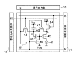
- FIG. 2 is a circuit diagram showing the internal configuration of the pixel circuit 15.
- the pixel circuit 15 of FIG. 2 has a light emitting unit 41 having an organic EL element, a drive transistor 42, a sampling transistor 43, a light emission control transistor 44, a holding capacity 45, and an auxiliary capacity 46.
- the pixel circuit 15 is formed on a semiconductor substrate such as silicon, and the drive transistor 42, the sampling transistor 43, and the light emission control transistor 44 are, for example, a epitaxial transistor. A power supply voltage is applied to the back gate of each transistor.
- the sampling transistor 43 writes in the holding capacitance 45 by sampling the signal voltage Vsig supplied from the signal output unit 18 via the signal line.
- the light emission control transistor 44 is connected between the power supply node of the power supply voltage Vcc and the source electrode of the drive transistor 42, and controls the light emission / non-light emission of the light emitting unit 41 under the drive by the light emission control signal DS.
- the holding capacity 45 is connected between the gate electrode and the source electrode of the drive transistor 42.
- the holding capacitance 45 holds the signal voltage Vsig written by sampling by the sampling transistor 43.
- the drive transistor 42 drives the light emitting unit 41 by passing a drive current corresponding to the holding voltage of the holding capacity 45 through the light emitting unit 41.
- the auxiliary capacitance 46 is connected between the source electrode of the drive transistor 42 and a node having a fixed potential, for example, a power node having a power supply voltage of Vcc.
- the auxiliary capacitance 46 suppresses fluctuations in the source potential of the drive transistor 42 when the signal voltage Vsig is written, and also acts to match the gate-source voltage Vgs of the drive transistor 42 with the threshold voltage Vth of the drive transistor 42. I do.
- FIG. 3 is a circuit diagram of a pixel circuit 15 having an internal configuration different from that of FIG.
- the light emission control transistor 44 is connected between the power supply potential Vcc and the source S of the drive transistor 42, and controls the on / off of the light emitting unit 41.
- the gate of the light emission control transistor 44 is connected to the scanning line DS.
- the sampling transistor 43 is connected between the signal line SL and the connection node A having the holding capacity 45 and the auxiliary capacity 46.
- the gate of the sampling transistor 43 is connected to the scanning line WS.
- the detection transistor 47 is connected between the connection node A and the source S of the drive transistor 42.
- the gate of the detection transistor 47 is connected to the scanning line AZ.
- the switching transistor 48 is connected between the gate G of the drive transistor 42 and a predetermined offset potential Vofs.
- the gate of the switching transistor 48 is connected to the scanning line AZ.
- the detection transistor 47 and the switching transistor 48 form a correction means for Vth cancellation.
- the holding capacity 45 is connected between the connection node A and the gate G of the drive transistor 42, and the auxiliary capacity 46 is connected between the power supply potential Vcc and the connection node A.
- the drive transistor 42 drives the light emitting unit 41 by passing a drain current Ids between the source / drain according to the gate voltage Vgs applied between the source / gate.
- the gate voltage Vgs of the drive transistor 42 is set according to the video signal Vsig supplied from the signal line SL, and the emission brightness of the light emitting unit 41 can be controlled according to the gradation of the video signal by the drain current Ids of the drive transistor 42. ..
- the threshold voltage Vth of the drive transistor 42 fluctuates for each pixel.
- the threshold voltage Vth of the drive transistor 42 is detected in advance and held in the holding capacity 45. After that, the sampling transistor 43 is turned on and the signal potential Vsig is written in the auxiliary capacitance 46. As a result, the gate potential Vgs corrected for the variation in the threshold voltage Vth of the drive transistor 42 is generated.
- FIGS. 2 and 3 are examples of the pixel circuit 15, and a pixel circuit 15 having an internal configuration other than those shown in FIGS. 2 and 3 can be applied to the pixel circuit 15 according to the present embodiment.
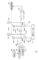
- FIG. 4 is a block diagram showing the internal configuration of the H-DRV unit 13.
- the H-DRV unit 13 includes a selector 49, a lamp buffer 51, a lamp generation DAC 52, a DAC 53 for Vofs, a temperature sensor 54, a lamp wiring 55, a plurality of voltage holding units 56, and a plurality of level shifters (LS). It has 57, a plurality of correction current sources 58, a comparator 59, and a current adjusting unit 60.
- the lamp buffer 51 uses the selector 49 to switch between an offset voltage for correcting the threshold value and mobility of the drive transistor 42 in the pixel circuit 15 and a lamp wave voltage at which the voltage level changes continuously. Later, it is buffered and output to the lamp wiring 55.
- a plurality of voltage holding units 56 and a plurality of switches 61 are connected to the lamp wiring 55.
- the plurality of voltage holding units 56 hold the voltage when the lamp wave voltage becomes a voltage corresponding to the gradation of the pixel circuit 15.
- the held voltage is the signal voltage and is supplied to the signal line 50.
- Each voltage holding unit 56 has a switch 56a. Each switch 56a in each voltage holding unit 56 is turned on or off according to the output voltage of the corresponding level shifter 57. A PWM signal corresponding to the gradation data of each pixel is input to the level shifter 57.
- the plurality of correction current sources 58 supply the correction current to the plurality of connection paths 55a between the lamp wiring 55 and the plurality of voltage holding units 56.
- the plurality of correction current sources 58 supply the same correction current to the plurality of connection paths 55a regardless of the brightness set in the plurality of pixel circuits 15.
- a plurality of switches 61 are provided between the plurality of correction current sources 58 and the plurality of connection paths 55a. These switches 61 can be turned on or off individually.
- the current adjusting unit 60 sets a predetermined brightness in the pixel circuit 15 connected to the predetermined connection path 55a depending on whether the correction current is passed through the plurality of connection paths 55a from the plurality of correction current sources 58 or not.
- the correction current is adjusted based on the voltage difference in the predetermined connection path 55a.
- the predetermined connection path 55a is, for example, the farthest connection path 55a on the lamp wiring 55 from the position of the lamp buffer 51.
- the predetermined brightness is, for example, white brightness.
- the current adjusting unit 60 may adjust the correction current a plurality of times, once in accordance with the scanning of the horizontal line, within the blanking period between two consecutive frames.
- the current adjusting unit 60 may include a first voltage detecting unit 62, a second voltage detecting unit 63, and a comparator 59.
- the first voltage detection unit 62 connects the farthest end from the lamp buffer 51 when setting the first luminance in the plurality of pixel circuits 15 without flowing the correction current from the plurality of correction current sources 58 into the plurality of connection paths 55a.
- the voltage of the path 55a is detected.
- the first luminance is, for example, white luminance.
- the second voltage detection unit 63 applies the correction current from the plurality of correction current sources 58 to the connection path 55a excluding the farthest connection path 55a, and applies the first brightness to the pixel circuit 15 connected to the farthest end connection path 55a.
- the voltage of the farthest end connection path 55a when the second brightness is set in the other pixel circuits 15 is detected.
- the second luminance is, for example, black luminance.
- the comparator 59 outputs a signal corresponding to the voltage difference between the voltage detected by the first voltage detection unit 62 and the voltage detected by the second voltage detection unit 63.
- the display device 1 according to the present embodiment has technical features in the internal configuration and operation of the H-DRV unit 13. Hereinafter, the internal configuration and operation of the H-DRV unit 13 of the present embodiment will be described in detail.
- the display device 1 according to the present embodiment supplies the offset voltage Vofs to the lamp wiring 55, corrects the threshold value and the mobility of the drive transistor 42 in the pixel circuit 15, and then supplies the lamp wave voltage to the signal voltage. Is adopted.
- a lamp buffer 51 that switches and outputs an offset voltage or a lamp wave voltage is connected to one end side of the lamp wiring 55.
- a plurality of signal lines are connected to the lamp wiring 55 via the plurality of voltage holding portions 56, but the longer the distance from the lamp buffer 51, the greater the wiring resistance on the lamp wiring 55. Therefore, for example, when the lamp buffer 51 supplies the lamp wave voltage to the lamp wiring 55, the voltage of the connection path 55a between the lamp wiring 55 and the plurality of voltage holding portions 56 may fluctuate depending on the position of the connection path 55a. be.
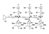
- FIG. 5 is an equivalent circuit diagram when three voltage holding units 56 are connected to the lamp wiring 55. Although omitted in FIG. 5, a pixel circuit 15 is connected to each voltage holding unit 56 via a corresponding signal line. Actually, a large number of voltage holding portions 56 are connected to the lamp wiring 55, but in FIG. 5, only three voltage holding portions 56 are shown for simplification.
- Each voltage holding unit 56 is equivalently represented by a switch 56a and a capacitance 56b.
- the capacitance 56b is a parasitic capacitance on the signal line 50.
- the wiring resistance R on the lamp wiring 55 is all equal in the connection path 55a between the lamp buffer 51 and the three voltage holding portions 56.
- the switch 61 between the plurality of correction current sources 58 and each connection path 55a so that the correction current from the correction current source 58 does not flow in the connection path 55a. Is off.
- Each voltage holding unit 56 holds the voltage level when the lamp wave voltage is sufficiently small. At this time, a current flows from each voltage holding unit 56 to the lamp buffer 51 via the lamp wiring 55.
- FIG. 5A it is assumed that the currents I flowing in the connection path 55a between the voltage holding portions 56 and the lamp wiring 55 are equal.
- the voltage drop in this section is I ⁇ R. Since a current of 2I flows between the connection path 55a at the latest end and the connection path 55a at the second farthest point from the lamp buffer 51, the voltage drop in this section is 2I ⁇ R. Since a current of 3I flows between the output ode of the lamp buffer 51 and the connection path 55a at the latest end, the voltage drop in this section is 3I ⁇ R.
- connection paths 55a with the plurality of voltage holding units 56 so that the voltage of each connection path 55a is different, and the lamp buffer 51 The farther the connection path 55a is, the higher the voltage level is. If there is a variation in the voltage of the connection path 55a with the plurality of voltage holding portions 56 on the lamp wiring 55, it becomes a factor that the brightness of the display screen varies.
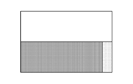
- FIG. 6 displays a white brightness image in the upper half of the display screen, displays a white brightness image in the area on one end side in the horizontal direction of the lower half, and displays a black brightness image in the remaining area of the lower half.
- An example is shown. It is assumed that one end side in the horizontal direction is the farthest end from the lamp buffer 51.
- FIG. 6 there is a difference in brightness between the white brightness of the upper half of the display screen and the white brightness of the lower half in the horizontal direction on one end side.
- the white brightness on one end side in the horizontal direction of the lower half is darker than the white brightness of the upper half.
- the white brightness on one end side in the horizontal direction of the lower half may be brighter than the white brightness of the upper half.
- Such a brightness difference is caused by the wiring resistance on the lamp wiring 55 and whether or not the correction current is supplied from the correction current source 58 to each connection path 55a.
- a luminance difference is referred to as horizontal crosstalk for convenience.
- FIG. 6 is a display example on the assumption that there is no shading phenomenon described in the second embodiment described later.
- the upper half of the screen displayed in white may be shaded with a gradual change in brightness in the horizontal direction.
- measures are taken to prevent horizontal crosstalk as shown in FIG.
- horizontal crosstalk is suppressed by supplying a correction current having an optimum amount of current from the plurality of correction current sources 58 to each connection path 55a with the plurality of voltage holding portions 56 on the lamp wiring 55. do.
- FIGS. 7A and 8 are diagrams schematically showing the operation of the current adjusting unit 60.
- a plurality of correction current sources 58 are connected via a plurality of switches 61 on a connection path 55a to which a plurality of voltage holding portions 56 on the lamp wiring 55 are connected.
- 7A and 8 show an example in which three correction current sources 58 are connected to three connection paths 55a via three switches 61 for simplification.
- the correction currents output by the plurality of correction current sources 58 are adjusted by the current adjusting unit 60.
- the plurality of correction current sources 58 output the same correction current.
- a switch 61 is provided between each correction current source 58 and the corresponding connection path 55a, and each switch 61 can be turned on or off individually. Therefore, whether or not the correction current is passed through each connection path 55a can be set for each connection path 55a.
- FIG. 7A shows an example in which white brightness is set in each pixel circuit 15.
- all the switches 61 of the correction current source 58 are turned off, and the switches 56a of the three voltage holding units 56 are turned on.
- a current flows from the voltage holding unit 56 to the lamp buffer 51 via the connection path 55a. Therefore, the voltage of the connection path 55a at the farthest end from the lamp buffer 51 becomes the highest.
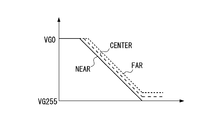
- FIG. 7B is a diagram schematically showing the voltage level of the connection path 55a with each voltage holding portion 56 on the lamp wiring 55.
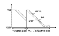
- the horizontal axis of FIG. 7B is time, and the vertical axis is voltage level. As shown in the figure, the voltage level becomes higher as the connection path 55a is farther from the lamp buffer 51.
- FIG. 7B shows an example of a lamp wave voltage in which the voltage level decreases from VG0 to VG255 with a constant slope, but a lamp wave voltage in which the voltage level rises from VG0 to VG255 with a constant slope may be used. Even in that case, the farther the connection path 55a is from the lamp buffer 51, the higher the voltage level of the lamp wave voltage.
- FIG. 8 shows an example in which white brightness is set for the farthest end pixel circuit 15 on the lamp wiring 55, and black brightness is set for the other pixel circuits 15.
- the switch 56a of the voltage holding unit 56 connected to the pixel circuit 15 for setting the black brightness is turned off, and the switch 61 of the correction current source 58 is turned on. Therefore, the voltage drop on the lamp wiring 55 does not occur, and the voltage rise of the connection path 55a at the farthest end from the lamp buffer 51 is also suppressed.
- the current adjusting unit 60 starts from the correction current source 58 so that the voltage of the farthest end connection path 55a in the case of FIG. 8 matches the voltage of the farthest end connection path 55a in the case of FIG. 7A. Adjust the output correction current. That is, when the black brightness is set (at the time of black raster), the voltage of the connection path 55a at the farthest end is intentionally raised. As a result, as shown in FIG. 6, when the upper half is white brightness, the lower half is white brightness on one end side in the horizontal direction and the remaining area is black brightness, the white brightness of the upper half and the one end side in the horizontal direction of the lower half are There is no difference in brightness from white brightness.
- FIG. 9 is a block diagram showing a schematic configuration of the current adjusting unit 60 according to the present embodiment.
- the current adjusting unit 60 includes a first voltage detecting unit 62, a second voltage detecting unit 63, a comparator 59, an adjusting signal generating unit 64, and an adjusting signal holding unit 65.
- the comparator 59 outputs a signal corresponding to the voltage difference between the voltage detected by the first voltage detection unit 62 and the voltage detected by the second voltage detection unit 63.
- the adjustment signal generation unit 64 generates a plurality of bits of adjustment signals for the current adjustment unit 60 to adjust the correction current based on the signal output from the comparator 59.
- the adjustment signal holding unit 65 holds the adjustment signal generated by the adjustment signal generation unit 64.
- the correction current source 58 outputs a correction current according to the adjustment signal.
- FIG. 10 is a block diagram showing the internal configuration of the current adjusting unit 60 of the sequential comparison method.
- the current adjustment unit 60 of FIG. 10 is an adjustment signal generation unit that generates a plurality of bits of adjustment signals based on the outputs of the plurality of DFFs (D-type flip-flops) 71 connected to the output paths of the comparator 59 and the outputs of the plurality of DFF 71s. It has 64 and a bias circuit 72 that generates a bias voltage based on an adjustment signal.
- DFFs D-type flip-flops
- the plurality of correction current sources 58 include a plurality of NMOS transistors 58a that control the correction current according to the bias voltage output from the bias circuit 72.
- a bias voltage is supplied to the gates of the NMOS transistors 58a, and each NMOS transistor 58a supplies the same correction current to each connection path 55a via the switch 61.
- the current adjusting unit 60 of FIG. 10 latches the output signal of the comparator 59 to any one of the plurality of DFF71s in order. Since the comparator 59 performs the comparison operation once for each horizontal line, the comparison results of the comparator 59 are latched in separate DFF71s for the number of horizontal lines corresponding to the number of the plurality of DFF71s.
- the adjustment signal generation unit 64 generates an adjustment signal composed of a plurality of bits based on the latch results of the plurality of DFF 71s.
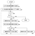
- FIG. 11 is a flowchart showing the processing operation of the current adjusting unit 60 of FIG. First, in a state where white brightness is set for all pixel circuits 15 connected to a certain horizontal line (at the time of white raster), the voltage of the connection path 55a between the voltage holding portion 56 at the farthest end from the lamp buffer 51 and the lamp wiring 55. Is detected (step S1). The process of step S1 is performed by the first voltage detection unit 62.
- step S2 the current amounts of the plurality of correction current sources 58 are initialized to K ⁇ 2 n-1 , and the variable j indicating the number of adjustments is initialized to n (step S2).
- step S3 the variable j indicating the number of adjustments is initialized to n.
- step S6 when driving all current sources (during black raster) that drive all the correction current sources 58 other than the correction current source 58 at the farthest end from the lamp buffer 51, the voltage holding unit 56 at the farthest end from the lamp buffer 51.
- the voltage of the connection path 55a with the lamp wiring 55 is detected (step S6).
- the process of step S6 is performed by the second voltage detection unit 63.
- step S7 it is determined whether or not the voltage detected in step S1 is higher than the voltage detected in step S6 (step S7).
- the determination process in step S7 is performed by the comparator 59, and the output of the comparator 59 indicates the determination result in step S7.
- step S7 If step S7 is YES, the j-th bit of the adjustment signal is changed to L (step S8). As a result, the correction current output from the correction current source 58 is adjusted. After that, the processes after step S3 are repeated.
- step S7 when step S7 is NO, the j-th bit of the adjustment signal is fixed to H (step S9), and the processes after step S3 are repeated.
- FIG. 12 is a block diagram showing the internal configuration of the current adjusting unit 60 of the charge pump control method.
- the current adjusting unit 60 of FIG. 12 includes a phase comparator 73 connected to the output path of the comparator 59, a charge pump 74, and a cascode current mirror circuit 75.
- the plurality of correction current sources 58 in FIG. 12 have a plurality of NMOS transistors operating at the same gate voltage, as in FIG. 10.
- the phase comparator 73 outputs a phase difference pulse between the output signal of the comparator 59 and the reference pulse signal that outputs a pulse at a timing determined for each horizontal line.
- the charge pump 74 controls the current source 76 so that the current source 76 in the bias voltage source 75 flows a constant current during the period of the phase difference pulse output from the phase comparator 73.
- the bias voltage source 75 has a PRIVATE transistor Q1 whose gate and drain are connected to the current source 76. A bias voltage is output from the gate of the epitaxial transistor Q1, and this bias voltage is input to the gate of each epitaxial transistor 58a of the correction current source 58.
- FIG. 13 is a flowchart showing the processing operation of the current adjusting unit 60 of FIG. First, in a state where white brightness is set for all pixel circuits 15 connected to a certain horizontal line (at the time of white raster), the voltage of the connection path 55a between the voltage holding portion 56 at the farthest end from the lamp buffer 51 and the lamp wiring 55. Is detected (step S11). The process of step S11 is performed by the first voltage detection unit 62.
- step S12 when the total current source 76 that drives all the correction current sources 58 other than the correction current source 58 at the farthest end from the lamp buffer 51 is driven (at the time of black raster), the voltage holding unit 56 at the farthest end from the lamp buffer 51 is driven. The voltage of the connection path 55a between the and the lamp wiring 55 is detected (step S12). The process of step S12 is performed by the second voltage detection unit 63.
- step S13 it is determined whether or not the voltage detected in step S11 is higher than the voltage detected in step S12 (step S13).
- the determination process in step S13 is performed by the comparator 59, and the output of the comparator 59 indicates the determination result in step S13.
- step S13 If step S13 is YES, control for increasing the correction current is performed (step S14), and the processes after step S12 are repeated. On the other hand, when step S13 is NO, control is performed to reduce the correction current (step S15).
- step S16 it is determined whether or not the correction current has been adjusted a specified number of times. If the specified number of times has not been reached, the processes after step S12 are repeated. If the specified number of times has been reached, the process ends.
- each connection is made from the plurality of correction current sources 58 based on the voltage difference of the connection path 55a with each voltage holding portion 56 on the lamp wiring 55 caused by the wiring resistance of the lamp wiring 55.
- the difference in brightness between the pixels can be made inconspicuous. More specifically, when the upper half area of the display screen is set to white brightness, the area on one end side in the horizontal direction of the lower half is set to white brightness, and the rest of the lower half is set to black brightness. , The brightness difference between the white brightness of the upper half and the white brightness of the region on one end side in the horizontal direction of the lower half can be made inconspicuous.
- the voltage of the connection path 55a with the voltage holding portion 56 connected to the lamp wiring 55 may be different between the side near the lamp buffer 51 and the side far from the lamp buffer 51 on the lamp wiring 55, and thus the display may be different. Shading may occur in which the brightness in the screen changes in the horizontal direction.
- FIG. 14 shows an example in which shading occurs when the entire display screen is displayed with white brightness.
- the second embodiment suppresses such shading.
- each voltage holding unit 56 connected to the lamp wiring 55 holds a signal voltage according to the gradation
- each voltage holding unit In order to suppress the horizontal crosstalk that occurs on the display screen due to the voltage difference between the connection path 55a of the 56 and the lamp wiring 55, the correction current supplied from each correction current source 58 to each connection path 55a is adjusted.
- the adjustment of the correction current in the first embodiment is performed within the period of supplying the lamp wave voltage to the lamp wiring 55.
- Each pixel circuit 15 causes the light emitting unit 41 to emit light with a brightness corresponding to the voltage difference between the offset voltage and the signal voltage.
- the signal voltage is corrected as a result by the correction current from the correction current source 58, and if the offset voltage is not corrected accordingly, the brightness of the light emitting unit 41 may vary. be.
- the plurality of correction current sources 58 are connected to the respective voltage holding portions 56 on the lamp wiring 55, as in the first embodiment.
- the correction current supplied to the connection path 55a is adjusted.
- the amount of correction current flowing from each correction current source 58 to each connection path 55a may be the same as that in the first embodiment. Therefore, the correction current determined by the method described in the first embodiment is applied from all the correction current sources 58 to the connection path 55a with each voltage holding portion 56 on the lamp wiring 55 during the supply period of the offset voltage. Supply.
- the current adjusting unit 60 described in the first embodiment can be applied as it is, and the current adjusting unit 60 described in the first embodiment is used to use the second embodiment. It is possible to take measures against horizontal shading.
- the offset voltage is a pulse voltage having a constant voltage level, and the offset voltage can be supplied to each pixel circuit 15 in a period shorter than the supply period of the lamp wave voltage, and the threshold value of the drive transistor 42 in each pixel circuit 15 can be supplied. Correction and mobility correction can be performed quickly.
- the third embodiment unlike the first and second embodiments, does not have the correction current source 58 and the current adjusting unit 60.
- the offset voltage in the first and second embodiments is a pulse voltage having a constant voltage level
- the offset voltage in the third embodiment is a voltage in which the voltage level changes continuously. That is, in the third embodiment, the offset voltage for performing the threshold value correction and the mobility correction of the drive transistor 42 in the pixel circuit 15 is set as a lamp wave.
- the display device 1 according to the third embodiment has an internal configuration of the H-DRV unit 13 different from that of the first and second embodiments.
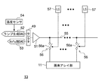
- FIG. 15 is a block diagram showing an internal configuration of the H-DRV unit 13 according to the third embodiment. Compared with FIG. 4, the H-DRV unit 13 of FIG. 15 does not include the correction current source 58, the switch 61, and the current adjusting unit 60.
- the DAC53 for Vofs connected to the input terminal of the lamp buffer 51 generates an offset voltage composed of a lamp wave. Therefore, the offset voltage supplied from the lamp buffer 51 to the lamp wiring 55 becomes a lamp wave whose voltage level continuously changes.
- FIG. 16 is a voltage waveform diagram on the lamp wiring 55. Times t1 to t2 are offset voltage supply periods, and times t2 to t3 are lamp wave voltage supply periods for generating signal voltages.
- the pixel circuit 15 holds the offset voltage on the lamp wiring 55, but holds the voltage before the voltage level of the offset voltage starts to drop, so that it is the same as the offset voltage used in the first and second embodiments.
- the offset voltage of the voltage level can be used to correct the threshold value and the mobility of the drive transistor 42.
- the voltage level of the connection path 55a with the plurality of voltage holding portions 56 on the lamp wiring 55 changes depending on the distance from the lamp buffer 51.
- the voltage difference of each connection path 55a during the period of supplying the offset voltage is the same as the voltage difference of each connection path 55a during the period of supplying the lamp wave voltage. Since each pixel circuit 15 emits light with a brightness corresponding to the voltage difference between the signal voltage and the offset voltage, the voltage difference due to the wiring resistance on the lamp wiring 55 is detected at the stage of detecting the voltage difference between the signal voltage and the offset voltage. It can be offset and the horizontal shading becomes less noticeable.
- the correction current source 58, the switch 61, and the current adjusting unit 60 are omitted from the H-DRV unit 13 of FIG. 4, and the offset voltage is changed to the lamp waveform.
- the light emitting unit 41 can emit light after canceling the voltage difference due to the wiring resistance on the lamp wiring 55, and the horizontal shading can be suppressed while having a simpler configuration than the second embodiment.
- the present technology can have the following configurations. (1) A plurality of pixel circuits arranged in at least one direction, and A plurality of signal lines that supply signal voltages according to gradation to the plurality of pixel circuits, and A voltage output unit that generates a ramp wave voltage whose voltage level changes with time, The lamp wiring that supplies the lamp wave voltage generated by the voltage output unit, and A plurality of voltage holding units connected between the lamp wiring and the plurality of signal lines, holding the lamp wave voltage at a timing corresponding to the brightness of the plurality of pixel circuits, and generating the signal voltage. A plurality of correction current sources that supply correction currents to a plurality of connection paths between the lamp wiring and the plurality of voltage holding units, and a plurality of correction current sources.
- a display device including a current adjusting unit that adjusts the correction current based on a voltage difference.
- the display device wherein the predetermined brightness is white brightness.
- the current adjusting unit is The voltage of the connection path at the farthest end is detected from the voltage output unit when the first luminance is set in the plurality of pixel circuits without flowing the correction current from the plurality of correction current sources to the plurality of connection paths. 1st voltage detector and The first brightness is set in a pixel circuit connected to the farthest connection path by passing the correction current from the plurality of correction current sources to a connection path other than the farthest connection path, and other pixel circuits. It has a second voltage detection unit that detects the voltage of the connection path at the farthest end when setting the second brightness.
- the current adjusting unit adjusts the correction current based on the voltage difference between the voltage detected by the first voltage detecting unit and the voltage detected by the second voltage detecting unit, (1) to (1).
- the display device according to any one of 3).
- the correction current is adjusted by the current adjusting unit so that the voltage detected by the second voltage detecting unit matches the voltage detected by the first voltage detecting unit, according to (4). Display device.
- the current adjusting unit increases the correction current to make the second voltage detecting unit larger.
- the current adjusting unit is A voltage comparator that outputs a signal corresponding to the voltage difference between the voltage detected by the first voltage detection unit and the voltage detected by the second voltage detection unit. Based on the signal output from the voltage comparator, the current adjusting unit has an adjusting signal generating unit that generates a multi-bit adjustment signal for adjusting the correction current.
- the display device according to any one of (4) to (6), wherein the current adjusting unit adjusts the correction current based on the adjusting signal.
- the display device (8) The display device according to (7), wherein the adjustment signal generation unit adjusts the adjustment signal bit by bit each time the correction current is adjusted.
- the current adjusting unit is A voltage comparator that outputs a signal corresponding to the voltage difference between the voltage detected by the first voltage detection unit and the voltage detected by the second voltage detection unit.
- a phase comparator that outputs a signal corresponding to the phase difference between the signal output from the voltage comparator and a predetermined reference signal, and It has a charge pump that outputs a voltage corresponding to a signal output from the phase comparator.
- the display device according to any one of (4) to (6), wherein the current adjusting unit adjusts the correction current based on the voltage output from the charge pump.
- the predetermined reference signal has a frequency corresponding to the scanning period of the horizontal line.
- the correction current source has a transistor that changes the correction current according to the gate voltage.
- the first luminance is white luminance.
- the voltage output unit outputs an offset voltage for correcting the characteristic variation of the plurality of pixel circuits to the lamp wiring before outputting the lamp wave voltage to the lamp wiring.
- the current adjusting unit supplies the correction current supplied by the plurality of correction current sources to the plurality of connection paths based on the voltage difference.
- the display device according to any one of (1) to (12) to be adjusted.
- the current adjusting unit performs the same correction current from the plurality of correction current sources depending on whether the voltage output unit supplies the offset voltage to the lamp wiring or the lamp voltage.
- the display device according to (13), which supplies a plurality of connection paths.
- the current adjusting unit adjusts the correction current a plurality of times, once in accordance with the scanning of the horizontal line, within the blanking period between two consecutive frames, (1) to (14). ).
- the display device according to any one of the items.
- Lamp wiring that switches between the offset voltage and the lamp wave voltage and supplies A plurality of voltage holding units connected between the lamp wiring and the plurality of signal lines, holding the lamp wave voltage at a timing corresponding to the brightness of the plurality of pixel circuits, and generating the signal voltage.
- a plurality of correction current sources that supply correction currents to a plurality of connection paths between the lamp wiring and the plurality of voltage holding units, and a plurality of correction current sources.
- the offset voltage and the ramp wave voltage are based on the voltage difference of the plurality of connection paths generated by the currents flowing from the plurality of voltage holding units to the voltage output units when setting predetermined brightness in the plurality of pixel circuits.
- a display device including a current adjusting unit that adjusts the correction current supplied by the plurality of correction current sources to the plurality of connection paths when supplying the lamp wiring.
Landscapes
- Engineering & Computer Science (AREA)
- Physics & Mathematics (AREA)
- Computer Hardware Design (AREA)
- General Physics & Mathematics (AREA)
- Theoretical Computer Science (AREA)
- Control Of Indicators Other Than Cathode Ray Tubes (AREA)
- Control Of El Displays (AREA)
- Vehicle Body Suspensions (AREA)
- Diaphragms For Electromechanical Transducers (AREA)
- Measuring Pulse, Heart Rate, Blood Pressure Or Blood Flow (AREA)
- Electroluminescent Light Sources (AREA)
Abstract
[課題]ランプ波電圧を用いて画素駆動を行う場合の表示品質を向上する。 [解決手段]表示装置は、少なくとも一方向に配置される複数の画素回路と、複数の画素回路に、階調に応じた信号電圧を供給する複数の信号線と、電圧レベルが時間に応じて変化するランプ波電圧を生成する電圧出力部と、電圧出力部で生成されたランプ波電圧を供給するランプ配線と、ランプ配線と複数の信号線との間に接続され、複数の画素回路の輝度に応じたタイミングでランプ波電圧を保持して信号電圧を生成する複数の電圧保持部と、ランプ配線と複数の電圧保持部との複数の接続経路に補正電流を供給する複数の補正電流源と、複数の補正電流源から補正電流を複数の接続経路に流す場合と流さない場合とにおいて、所定の接続経路に繋がる画素回路に所定の輝度を設定する際の所定の接続経路での電圧差に基づいて、補正電流を調整する電流調整部と、を備える。
Description
本開示は、表示装置に関する。
有機EL(Electroluminescence)装置や液晶表示装置では、画質に対する要求が高まっており、画質向上のための種々の工夫がなされている。例えば、有機EL装置は、自発光素子を用いることから、液晶表示装置よりもコントラストに優れているが、自発光素子を駆動するための画素回路内のトランジスタの閾値電圧や移動度に製造上のばらつきが生じるため、これらのばらつきを補正するための画素回路が開発されている(特許文献1参照)。
しかしながら、表示画面の同一の水平ラインに、輝度が著しく異なる画像を表示させる場合、隣接画素の影響を受けて、本来の輝度とは異なる明るさで表示される場合がある。例えば、表示画面の左端側又は右端側の一部の画素領域と、残りの画素領域とで、輝度が著しく異なる画像を表示させる場合、一部の画素領域だけ本来の輝度とは異なる明るさで表示され、一部の表示領域の境界部分に筋が視認されることがある。
この現象は、1水平ライン上の全画素に繋がるランプ配線にランプ波電圧を供給して、各画素の輝度に応じた信号電圧を画素ごとに保持する方式の画素駆動を行う場合に生じる。具体的には、ランプ配線の配線抵抗や画素負荷容量による電圧降下が原因で生じる。
そこで、本開示では、ランプ波電圧を用いて画素駆動を行う場合の表示品質を向上できる表示装置を提供するものである。
上記の課題を解決するために、本開示によれば、少なくとも一方向に配置される複数の画素回路と、
前記複数の画素回路に、階調に応じた信号電圧を供給する複数の信号線と、
電圧レベルが時間に応じて変化するランプ波電圧を生成する電圧出力部と、
前記電圧出力部で生成された前記ランプ波電圧を供給するランプ配線と、
前記ランプ配線と前記複数の信号線との間に接続され、前記複数の画素回路の輝度に応じたタイミングで前記ランプ波電圧を保持して前記信号電圧を生成する複数の電圧保持部と、
前記ランプ配線と前記複数の電圧保持部との複数の接続経路に補正電流を供給する複数の補正電流源と、
前記複数の補正電流源から前記補正電流を前記複数の接続経路に流す場合と流さない場合とにおいて、所定の接続経路に繋がる画素回路に所定の輝度を設定する際の前記所定の接続経路での電圧差に基づいて、前記補正電流を調整する電流調整部と、を備える表示装置が提供される。
前記複数の画素回路に、階調に応じた信号電圧を供給する複数の信号線と、
電圧レベルが時間に応じて変化するランプ波電圧を生成する電圧出力部と、
前記電圧出力部で生成された前記ランプ波電圧を供給するランプ配線と、
前記ランプ配線と前記複数の信号線との間に接続され、前記複数の画素回路の輝度に応じたタイミングで前記ランプ波電圧を保持して前記信号電圧を生成する複数の電圧保持部と、
前記ランプ配線と前記複数の電圧保持部との複数の接続経路に補正電流を供給する複数の補正電流源と、
前記複数の補正電流源から前記補正電流を前記複数の接続経路に流す場合と流さない場合とにおいて、所定の接続経路に繋がる画素回路に所定の輝度を設定する際の前記所定の接続経路での電圧差に基づいて、前記補正電流を調整する電流調整部と、を備える表示装置が提供される。
前記複数の補正電流源は、前記ランプ波電圧を前記ランプ配線に供給する際には、前記複数の画素回路に設定される輝度によらず、同一の前記補正電流を前記複数の接続経路に供給してもよい。
前記所定の接続経路は、前記電圧出力部の位置から前記ランプ配線上の最遠端の接続経路であり、
前記所定の輝度は、白色輝度であってもよい。
前記所定の輝度は、白色輝度であってもよい。
前記電流調整部は、
前記複数の補正電流源から前記補正電流を前記複数の接続経路に流さずに前記複数の画素回路に第1輝度を設定する際の前記電圧出力部から最遠端の前記接続経路の電圧を検出する第1電圧検出部と、
前記複数の補正電流源から前記最遠端の接続経路を除く接続経路に前記補正電流を流して前記最遠端の接続経路に繋がる画素回路に前記第1輝度を設定し、それ以外の画素回路に第2輝度を設定する際の前記最遠端の接続経路の電圧を検出する第2電圧検出部と、を有し、
前記電流調整部は、前記第1電圧検出部で検出された電圧と、前記第2電圧検出部で検出された電圧との電圧差に基づいて、前記補正電流を調整してもよい。
前記複数の補正電流源から前記補正電流を前記複数の接続経路に流さずに前記複数の画素回路に第1輝度を設定する際の前記電圧出力部から最遠端の前記接続経路の電圧を検出する第1電圧検出部と、
前記複数の補正電流源から前記最遠端の接続経路を除く接続経路に前記補正電流を流して前記最遠端の接続経路に繋がる画素回路に前記第1輝度を設定し、それ以外の画素回路に第2輝度を設定する際の前記最遠端の接続経路の電圧を検出する第2電圧検出部と、を有し、
前記電流調整部は、前記第1電圧検出部で検出された電圧と、前記第2電圧検出部で検出された電圧との電圧差に基づいて、前記補正電流を調整してもよい。
前記電流調整部は、前記第2電圧検出部で検出された電圧が前記第1電圧検出部で検出された電圧に一致するように前記補正電流を調整してもよい。
前記電流調整部は、前記第2電圧検出部で検出された電圧が前記第1電圧検出部で検出された電圧よりも低い場合には、前記補正電流をより大きくし、前記第2電圧検出部で検出された電圧が前記第1電圧検出部で検出された電圧よりも高い場合には、前記補正電流をより小さくする処理を、水平ラインの走査に合わせて1回ずつ複数回行ってもよい。
前記電流調整部は、
前記第1電圧検出部で検出された電圧と、前記第2電圧検出部で検出された電圧との電圧差に応じた信号を出力する電圧比較器と、
前記電圧比較器から出力された信号に基づいて、前記電流調整部が前記補正電流を調整するための複数ビットの調整信号を生成する調整信号生成部と、を有し、
前記電流調整部は、前記調整信号に基づいて前記補正電流を調整してもよい。
前記第1電圧検出部で検出された電圧と、前記第2電圧検出部で検出された電圧との電圧差に応じた信号を出力する電圧比較器と、
前記電圧比較器から出力された信号に基づいて、前記電流調整部が前記補正電流を調整するための複数ビットの調整信号を生成する調整信号生成部と、を有し、
前記電流調整部は、前記調整信号に基づいて前記補正電流を調整してもよい。
前記調整信号生成部は、前記補正電流の調整のたびに、前記調整信号を1ビットずつ調整してもよい。
前記電流調整部は、
前記第1電圧検出部で検出された電圧と、前記第2電圧検出部で検出された電圧との電圧差に応じた信号を出力する電圧比較器と、
前記電圧比較器から出力された信号と、所定の基準信号との位相差に応じた信号を出力する位相比較器と、
前記位相比較器から出力された信号に応じた電圧を出力するチャージポンプと、を有し、
前記電流調整部は、前記チャージポンプから出力された電圧に基づいて、前記補正電流を調整してもよい。
前記第1電圧検出部で検出された電圧と、前記第2電圧検出部で検出された電圧との電圧差に応じた信号を出力する電圧比較器と、
前記電圧比較器から出力された信号と、所定の基準信号との位相差に応じた信号を出力する位相比較器と、
前記位相比較器から出力された信号に応じた電圧を出力するチャージポンプと、を有し、
前記電流調整部は、前記チャージポンプから出力された電圧に基づいて、前記補正電流を調整してもよい。
前記所定の基準信号は、水平ラインの走査期間に応じた周波数を有し、
前記電圧比較器は、水平ラインに1回の割合で、前記電圧差に応じた信号を出力してもよい。
前記電圧比較器は、水平ラインに1回の割合で、前記電圧差に応じた信号を出力してもよい。
前記補正電流源は、ゲート電圧に応じて前記補正電流を可変させるトランジスタを有し、
前記チャージポンプから出力された電圧により、前記ゲート電圧を制御するバイアス回路をさらに備えてもよい。
前記チャージポンプから出力された電圧により、前記ゲート電圧を制御するバイアス回路をさらに備えてもよい。
前記第1輝度は白色の輝度であり、
前記第2輝度は黒色の輝度であってもよい。
前記第2輝度は黒色の輝度であってもよい。
前記電圧出力部は、前記ランプ配線に前記ランプ波電圧を出力する前に、前記複数の画素回路の特性ばらつきを補正するためのオフセット電圧を前記ランプ配線に出力し、
前記電流調整部は、前記電圧出力部が前記オフセット電圧を前記ランプ配線に供給する際に、前記電圧差に基づいて、前記複数の補正電流源が前記複数の接続経路に供給する前記補正電流を調整してもよい。
前記電流調整部は、前記電圧出力部が前記オフセット電圧を前記ランプ配線に供給する際に、前記電圧差に基づいて、前記複数の補正電流源が前記複数の接続経路に供給する前記補正電流を調整してもよい。
前記電流調整部は、前記電圧出力部が前記ランプ配線に前記オフセット電圧を供給する場合と前記ランプ電圧を供給する場合とで、同一の前記補正電流を前記複数の補正電流源から前記複数の接続経路に供給してもよい。
前記電流調整部は、連続する2つのフレームの間のブランキング期間内に、水平ラインの走査に合わせて一回ずつ複数回にわたって、前記補正電流を調整してもよい。
本開示によれば、少なくとも一方向に配置される複数の画素回路と、
前記複数の画素回路に、階調に応じた信号電圧を供給する複数の信号線と、
前記複数の画素回路の特性ばらつきを補正するためのオフセット電圧と、電圧レベルが時間に応じて変化するランプ波電圧とを生成する電圧出力部と、
前記オフセット電圧と前記ランプ波電圧とを切り替えて供給するランプ配線と、
前記ランプ配線と前記複数の信号線との間に接続され、前記複数の画素回路の輝度に応じたタイミングで前記ランプ波電圧を保持して前記信号電圧を生成する複数の電圧保持部と、
前記ランプ配線と前記複数の電圧保持部との複数の接続経路に補正電流を供給する複数の補正電流源と、
前記複数の画素回路に所定の輝度を設定する際に前記複数の電圧保持部から前記電圧出力部に流れる電流によって生じる前記複数の接続経路の電圧差に基づいて、前記オフセット電圧及び前記ランプ波電圧を前記ランプ配線に供給する際に前記複数の補正電流源が前記複数の接続経路に供給する前記補正電流を調整する電流調整部と、を備える表示装置が提供される。
前記複数の画素回路に、階調に応じた信号電圧を供給する複数の信号線と、
前記複数の画素回路の特性ばらつきを補正するためのオフセット電圧と、電圧レベルが時間に応じて変化するランプ波電圧とを生成する電圧出力部と、
前記オフセット電圧と前記ランプ波電圧とを切り替えて供給するランプ配線と、
前記ランプ配線と前記複数の信号線との間に接続され、前記複数の画素回路の輝度に応じたタイミングで前記ランプ波電圧を保持して前記信号電圧を生成する複数の電圧保持部と、
前記ランプ配線と前記複数の電圧保持部との複数の接続経路に補正電流を供給する複数の補正電流源と、
前記複数の画素回路に所定の輝度を設定する際に前記複数の電圧保持部から前記電圧出力部に流れる電流によって生じる前記複数の接続経路の電圧差に基づいて、前記オフセット電圧及び前記ランプ波電圧を前記ランプ配線に供給する際に前記複数の補正電流源が前記複数の接続経路に供給する前記補正電流を調整する電流調整部と、を備える表示装置が提供される。
以下、図面を参照して、表示装置の実施形態について説明する。以下では、表示装置の主要な構成部分を中心に説明するが、表示装置には、図示又は説明されていない構成部分や機能が存在しうる。以下の説明は、図示又は説明されていない構成部分や機能を除外するものではない。
(第1の実施形態)
図1は第1の実施形態による表示装置1を備えた表示システム2の概略構成を示すブロック図である。図1の表示システム2は、マイクロOLED(Organic Light Emitting Diode)システムの構成を示している。なお、本実施形態による表示装置1は、TVやPCモニタ等の大画面の表示装置1を備えた表示システム2にも適用可能である。
図1は第1の実施形態による表示装置1を備えた表示システム2の概略構成を示すブロック図である。図1の表示システム2は、マイクロOLED(Organic Light Emitting Diode)システムの構成を示している。なお、本実施形態による表示装置1は、TVやPCモニタ等の大画面の表示装置1を備えた表示システム2にも適用可能である。
図1の表示システム2は、表示装置1と、ディスプレイコントローラ3と、タイミングコントローラ4と、データ入出力I/F部5とを備えている。なお、図1では、ディスプレイコントローラ3等を表示装置1とは別体にしているが、ディプレイコントローラ等を表示装置1に統合させてもよい。
表示装置1は、画素アレイ部11と、V-DRV部12と、H-DRV部13と、信号処理部14と、を有する。
画素アレイ部11は、水平方向及び垂直方向に配置される複数の画素回路15を有する。各画素回路15は、例えば有機EL素子等の発光部と、発光部を制御する複数のトランジスタと、複数の容量とを有する。画素回路15の内部構成は後述する。
信号処理部14は、画素アレイ部11に表示されるべき映像信号の信号処理を行う。信号処理の具体的内容は問わないが、例えばガンマ補正などである。信号処理部14で信号処理された映像信号は、H-DRV部13に送られる。
V-DRV部12は、後述する図2及び図3に示すように、書き込み走査部16と駆動走査部17とを有する。書き込み走査部16は、各画素回路15に信号電圧を書き込むに際して、各走査線に書き込み走査信号を順次供給して、各走査線WS1~WSnを順次駆動する。駆動走査部17は、書き込み走査部16による線順次走査に同期して、各駆動線に発光制御信号を供給し、発光部の発光と非発光を制御する。
H-DRV部13は、図2及び図3に示すように信号出力部18を有する。信号出力部18は、ランプ波電圧を、各画素の階調に応じたタイミングで保持して信号電圧を生成する。信号出力部18は、信号電圧又はオフセット電圧Vofsを選択的に選択して、対応する信号線に供給する。オフセット電圧Vofsは、信号電圧の基準となる電圧(例えば、映像信号の黒レベルに相当する電圧)であり、後述する閾値補正動作を行うために用いられる。
信号出力部18から択一的に出力される信号電圧又はオフセット電圧Vofsは、信号線を介して各画素回路15に供給され、書き込み走査部16による走査で選択された行単位で、各画素回路15に設定される。
ディスプレイコントローラ3は、HLOGIC部21とVLOGIC部22を有し、画素アレイ部11に対する表示制御を行う。
HLOGIC部21は、映像信号をH-DRV部13に供給する。VLOGIC部22は、走査線及び駆動線のタイミングを規定する信号をV-DRV部12に供給する。
タイミングコントローラ4は、クロック生成器23と、タイミング生成器24と、画像処理部25とを有する。クロック生成器23は、表示装置1の垂直同期クロックと水平同期クロックを生成して、ディスプレイコントローラ3に供給する。タイミング生成器24は、ディスプレイコントローラ3の動作タイミングを規定する信号を生成して、ディスプレイコントローラ3に供給する。画像処理部25は、データ入出力I/F部5に入力された映像信号に対して、種々の画像処理を施す。画像処理を行った後の映像信号は、ディスプレイコントローラ3内のHLOGIC部21に供給される。
データ入出力I/F部5は、画像I/F部31と、データS/P部32と、クロック制御部33と、H/V同期部34とを有する。画像I/F部31は、外部からの映像信号を受信する。映像信号は、シリアルのデジタルデータである。データS/P部32は、映像信号をパラレルデータに変換した後、タイミングコントローラ4内の画像処理部25に送る。クロック制御部33は、表示装置1の表示周波数に適合するクロックを生成する。H/V同期部34は、表示装置1の水平同期タイミングと垂直同期タイミングを規定する信号を生成して、タイミング生成器24に送る。
図2は画素回路15の内部構成を示す回路図である。図2の画素回路15は、有機EL素子を有する発光部41と、駆動トランジスタ42と、サンプリングトランジスタ43と、発光制御トランジスタ44と、保持容量45と、補助容量46とを有する。画素回路15は、シリコン等の半導体基板上に形成され、駆動トランジスタ42、サンプリングトランジスタ43及び発光制御トランジスタ44は例えばPMOSトランジスタである。各トランジスタはバックゲートには電源電圧が印加されている。
サンプリングトランジスタ43は、信号出力部18から信号線を介して供給される信号電圧Vsigをサンプリングすることによって保持容量45に書き込む。発光制御トランジスタ44は、電源電圧Vccの電源ノードと駆動トランジスタ42のソース電極との間に接続され、発光制御信号DSによる駆動の下に、発光部41の発光/非発光を制御する。
保持容量45は、駆動トランジスタ42のゲート電極とソース電極との間に接続されている。この保持容量45は、サンプリングトランジスタ43によるサンプリングによって書き込まれた信号電圧Vsigを保持する。駆動トランジスタ42は、保持容量45の保持電圧に応じた駆動電流を発光部41に流すことによって発光部41を駆動する。補助容量46は、駆動トランジスタ42のソース電極と、固定電位のノード、例えば、電源電圧Vccの電源ノードとの間に接続されている。この補助容量46は、信号電圧Vsigを書き込んだときに駆動トランジスタ42のソース電位が変動するのを抑制するとともに、駆動トランジスタ42のゲート-ソース間電圧Vgsを駆動トランジスタ42の閾値電圧Vthに合わせる作用を行う。
画素回路15の内部構成は図2に示したものに限定されない。例えば、図3は図2とは異なる内部構成を有する画素回路15の回路図である。発光制御トランジスタ44は電源電位Vccと駆動トランジスタ42のソースSとの間に接続されており、発光部41のオン/オフを制御する。発光制御トランジスタ44のゲートは走査線DSに接続されている。
サンプリングトランジスタ43は信号線SLと、保持容量45及び補助容量46の接続ノードAとの間に接続されている。サンプリングトランジスタ43のゲートは走査線WSに接続されている。接続ノードAと駆動トランジスタ42のソースSとの間に検出トランジスタ47が接続されている。検出トランジスタ47のゲートは走査線AZに接続されている。スイッチングトランジスタ48は、駆動トランジスタ42のゲートGと所定のオフセット電位Vofsとの間に接続されている。スイッチングトランジスタ48のゲートは走査線AZに接続されている。検出トランジスタ47とスイッチングトランジスタ48はVthキャンセル用の補正手段を構成している。保持容量45は接続ノードAと駆動トランジスタ42のゲートGとの間に接続され、補助容量46は電源電位Vccと接続ノードAとの間に接続されている。
駆動トランジスタ42はソース/ゲート間に印加されるゲート電圧Vgsに応じてソース/ドレイン間にドレイン電流Idsを流して、発光部41を駆動する。信号線SLから供給される映像信号Vsigに応じて駆動トランジスタ42のゲート電圧Vgsが設定され、駆動トランジスタ42のドレイン電流Idsにより、映像信号の階調に応じて発光部41の発光輝度を制御できる。
駆動トランジスタ42の閾値電圧Vthは画素毎に変動する。この閾値電圧をキャンセルするため、予め駆動トランジスタ42の閾値電圧Vthを検出し、保持容量45に保持しておく。この後サンプリングトランジスタ43をオンして補助容量46に信号電位Vsigを書き込む。これにより、駆動トランジスタ42の閾値電圧Vthのばらつきを補正したゲート電位Vgsが生成される。
図2及び図3は、画素回路15の一例であり、本実施形態による画素回路15には、図2及び図3以外の内部構成の画素回路15も適用可能である。
図4はH-DRV部13の内部構成を示すブロック図である。H-DRV部13は、セレクタ49と、ランプバッファ51と、ランプ生成DAC52と、Vofs用DAC53と、温度センサ54と、ランプ配線55と、複数の電圧保持部56と、複数のレベルシフタ(LS)57と、複数の補正電流源58と、コンパレータ59と、電流調整部60とを有する。
ランプバッファ51は、画素回路15内の駆動トランジスタ42の閾値補正と移動度補正を行うためのオフセット電圧と、電圧レベルが連続的に変化するランプ波電圧との一方を、セレクタ49にて切り替えた後に、バッファリングしてランプ配線55に出力する。
ランプ配線55には、複数の電圧保持部56と、複数のスイッチ61とが接続されている。複数の電圧保持部56は、ランプ波電圧が画素回路15の階調に応じた電圧になった時点で、その電圧を保持する。保持された電圧が信号電圧であり、信号線50に供給される。
各電圧保持部56はスイッチ56aを有する。各電圧保持部56内の各スイッチ56aは、対応するレベルシフタ57の出力電圧に応じてオンまたはオフする。レベルシフタ57には、各画素の階調データに応じたPWM信号が入力される。
複数の補正電流源58は、ランプ配線55と複数の電圧保持部56との複数の接続経路55aに補正電流を供給する。複数の補正電流源58は、ランプ波電圧をランプ配線55に供給する際には、複数の画素回路15に設定される輝度によらず、同一の補正電流を複数の接続経路55aに供給する。
複数の補正電流源58と複数の接続経路55aとの間には、複数のスイッチ61が設けられている。これらのスイッチ61は個別にオン又はオフすることができる。
電流調整部60は、複数の補正電流源58から補正電流を複数の接続経路55aに流す場合と流さない場合とにおいて、所定の接続経路55aに繋がる画素回路15に所定の輝度を設定する際の所定の接続経路55aでの電圧差に基づいて、補正電流を調整する。所定の接続経路55aは、例えばランプバッファ51の位置からランプ配線55上の最遠端の接続経路55aである。所定の輝度は、例えば白色輝度である。
電流調整部60は、連続する2つのフレームの間のブランキング期間内に、水平ラインの走査に合わせて一回ずつ複数回にわたって、補正電流を調整するようにしてもよい。
電流調整部60は、第1電圧検出部62と、第2電圧検出部63と、コンパレータ59とを有してもよい。
第1電圧検出部62は、複数の補正電流源58から補正電流を複数の接続経路55aに流さずに複数の画素回路15に第1輝度を設定する際のランプバッファ51から最遠端の接続経路55aの電圧を検出する。第1輝度は、例えば白色輝度である。
第2電圧検出部63は、複数の補正電流源58から最遠端の接続経路55aを除く接続経路55aに補正電流を流して最遠端の接続経路55aに繋がる画素回路15に第1輝度を設定し、それ以外の画素回路15に第2輝度を設定する際の最遠端の接続経路55aの電圧を検出する。第2輝度は、例えば黒色輝度である。
コンパレータ59は、第1電圧検出部62で検出された電圧と、第2電圧検出部63で検出された電圧との電圧差に応じた信号を出力する。
本実施形態による表示装置1は、H-DRV部13の内部構成及び動作に技術的特徴がある。以下、本実施形態のH-DRV部13の内部構成及び動作を詳細に説明する。本実施形態による表示装置1は、ランプ配線55にオフセット電圧Vofsを供給して、画素回路15内の駆動トランジスタ42の閾値補正と移動度補正を行った後に、ランプ波電圧を供給して信号電圧を生成する方式を採用している。
ランプ配線55の一端側には、オフセット電圧又はランプ波電圧を切り替えて出力するランプバッファ51が接続されている。ランプ配線55には、複数の電圧保持部56を介して複数の信号線が接続されているが、ランプバッファ51からの距離が長いほど、ランプ配線55上の配線抵抗が大きくなる。このため、例えば、ランプバッファ51がランプ配線55にランプ波電圧を供給する場合、ランプ配線55と複数の電圧保持部56との接続経路55aの電圧が、接続経路55aの位置によって変動する場合がある。
図5はランプ配線55に3つの電圧保持部56を接続した場合の等価回路図である。図5では省略しているが、各電圧保持部56には、対応する信号線を介して画素回路15が接続されている。実際には、ランプ配線55に多数の電圧保持部56が接続されるが、図5では簡略化して3つの電圧保持部56のみを図示している。各電圧保持部56は、等価的にはスイッチ56aと容量56bで表される。容量56bは、信号線50上の寄生容量である。
図5では、ランプ配線55上の配線抵抗Rが、ランプバッファ51と3つの電圧保持部56との接続経路55aですべて等しいと仮定している。例えば、各画素回路15に白色の輝度を設定する場合、補正電流源58からの補正電流が接続経路55aに流れないように、複数の補正電流源58と各接続経路55aとの間のスイッチ61はオフである。各電圧保持部56は、ランプ波電圧が十分に小さいときの電圧レベルを保持する。このとき、各電圧保持部56からランプ配線55を介してランプバッファ51に電流が流れる。図5Aでは、各電圧保持部56とランプ配線55との接続経路55aに流れる電流Iが等しいと仮定している。ランプバッファ51から最遠端の接続経路55aと2番目に遠い接続経路55aとの間には、電流Iが流れるため、この区間内の電圧降下はI×Rである。ランプバッファ51から最近端の接続経路55aと2番目に遠い接続経路55aとの間には、2Iの電流が流れるため、この区間内の電圧降下は2I×Rである。ランプバッファ51の出力オードから最近端の接続経路55aとの間には、3Iの電流が流れるため、この区間内の電圧降下は3I×Rである。
このように、各画素に白色の輝度を設定する場合には、複数の電圧保持部56との接続経路55a間に電圧降下が生じるために、各接続経路55aの電圧が相違し、ランプバッファ51から遠い接続経路55aほど、電圧レベルが高くなる。ランプ配線55上の複数の電圧保持部56との接続経路55aの電圧にばらつきがあると、表示画面の輝度ばらつきが生じる要因になる。
例えば、図6は表示画面の上半分に白色輝度の画像を表示し、下半分の水平方向一端側の領域に白色輝度の画像を表示し、下半分の残りの領域に黒色輝度の画像を表示する例を示している。水平方向一端側は、ランプバッファ51から最遠端の場所であるとする。
図6の例では、表示画面の上半分の白色輝度と、下半分の水平方向一端側の白色輝度とに明るさの違いが生じる。実際には、下半分の水平方向一端側の白色輝度が、上半分の白色輝度よりも暗くなる例を示している。場合によっては、下半分の水平方向一端側の白色輝度が、上半分の白色輝度よりも明るくなる場合もありうる。
このような輝度差は、ランプ配線55上の配線抵抗と、補正電流源58から各接続経路55aに補正電流を供給するか否かによって生じる。本明細書では、このような輝度差を便宜上、水平方向クロストークと呼ぶ。
なお、図6は、後述する第2の実施形態で説明するシェーディング現象がないと仮定した場合の表示例である。実際には、白色で表示される画面の上半分の表示領域は、水平方向に輝度が徐々に変化するシェーディングが生じるおそれがある。
本実施形態は、図6のような水平方向クロストークが生じないように対策を行うものである。本実施形態では、ランプ配線55上の複数の電圧保持部56との各接続経路55aに、複数の補正電流源58から最適な電流量の補正電流を供給することで、水平方向クロストークを抑制する。
図7A及び図8は電流調整部60の動作を模式的に示す図である。図7A及び図8に示すように、ランプ配線55上の複数の電圧保持部56が接続される接続経路55a上に、複数のスイッチ61を介して複数の補正電流源58が接続されている。図7Aと図8は、簡略化のために、3つの接続経路55aに3つのスイッチ61を介して3つの補正電流源58が接続されている例を示している。複数の補正電流源58が出力する補正電流は、電流調整部60で調整される。複数の補正電流源58は、同一の補正電流を出力する。各補正電流源58と、対応する接続経路55aとの間には、スイッチ61が設けられており、各スイッチ61は個別にオン又はオフすることができる。よって、各接続経路55aに補正電流を流すか否かは、接続経路55aごとに設定することができる。
図7Aは各画素回路15に白色輝度を設定する例を示している。この場合、補正電流源58のスイッチ61をすべてオフし、かつ3つの電圧保持部56のスイッチ56aをオンする。これにより、図6と同様に、電圧保持部56から接続経路55aを介してランプバッファ51に電流が流れる。このため、ランプバッファ51から最遠端の接続経路55aの電圧が最も高くなる。図7Bは、ランプ配線55上の各電圧保持部56との接続経路55aの電圧レベルを模式的に示す図である。図7Bの横軸は時間、縦軸は電圧レベルである。図示のように、ランプバッファ51から遠い接続経路55aほど、電圧レベルが高くなる。図7Bは、VG0からVG255まで電圧レベルが一定の傾きで下がるランプ波電圧の一例を示しているが、VG0からVG255まで電圧レベルが一定の傾きで上がるランプ波電圧を用いてもよい。その場合でも、ランプバッファ51から遠い接続経路55aほど、ランプ波電圧の電圧レベルが高くなる。
図8はランプ配線55上の最遠端の画素回路15には白色輝度を設定し、それ以外の画素回路15には黒色輝度を設定する例を示している。この場合、黒色輝度を設定する画素回路15に接続される電圧保持部56のスイッチ56aはオフし、補正電流源58のスイッチ61はオンする。このため、ランプ配線55上の電圧降下は起きなくなり、ランプバッファ51から最遠端の接続経路55aの電圧上昇も抑制される。
本実施形態による電流調整部60は、図8の場合の最遠端の接続経路55aの電圧が図7Aの場合の最遠端の接続経路55aの電圧に一致するように、補正電流源58から出力される補正電流を調整する。すなわち、黒輝度の設定時(黒ラスタ時)に、意図的に最遠端の接続経路55aの電圧を引き上げる。これにより、図6のように、上半分が白色輝度で、下半分の水平方向一端側が白色輝度で残りの領域が黒色輝度の場合に、上半分の白色輝度と下半分の水平方向一端側の白色輝度との明るさの違いがなくなる。
図9は本実施形態による電流調整部60の概略構成を示すブロック図である。電流調整部60は、第1電圧検出部62と、第2電圧検出部63と、コンパレータ59と、調整信号生成部64と、調整信号保持部65とを有する。
上述したように、コンパレータ59は、第1電圧検出部62で検出された電圧と、第2電圧検出部63で検出された電圧との電圧差に応じた信号を出力する。調整信号生成部64は、コンパレータ59から出力された信号に基づいて、電流調整部60が補正電流を調整するための複数ビットの調整信号を生成する。調整信号保持部65は、調整信号生成部64が生成した調整信号を保持する。補正電流源58は、調整信号に応じた補正電流を出力する。
電流調整部60の具体的な動作方式として、逐次比較方式とチャージポンプ制御方式が考えられる。以下、順に説明する。
図10は逐次比較方式の電流調整部60の内部構成を示すブロック図である。図10の電流調整部60は、コンパレータ59の出力経路に接続された複数のDFF(D型フリップフロップ)71と、複数のDFF71の出力に基づいて複数ビットの調整信号を生成する調整信号生成部64と、調整信号に基づいてバイアス電圧を生成するバイアス回路72とを有する。
複数の補正電流源58は、バイアス回路72から出力されたバイアス電圧に応じて補正電流を制御する複数のNMOSトランジスタ58aを有する。これらNMOSトランジスタ58aのゲートにバイアス電圧が供給され、各NMOSトランジスタ58aは、同一の補正電流をスイッチ61を介して各接続経路55aに供給する。
図10の電流調整部60は、コンパレータ59の出力信号を、複数のDFF71のいずれか一つに順繰りにラッチする。コンパレータ59は、1水平ラインに1回ずつ比較動作を行うため、複数のDFF71の数分の水平ライン数について、コンパレータ59での比較結果をそれぞれ別個のDFF71にラッチする。調整信号生成部64は、複数のDFF71のラッチ結果に基づいて、複数ビットからなる調整信号を生成する。
図11は図10の電流調整部60の処理動作を示すフローチャートである。まず、ある水平ラインに接続された全画素回路15に白色輝度を設定した状態(白ラスタ時)で、ランプバッファ51から最遠端の電圧保持部56とランプ配線55との接続経路55aの電圧を検出する(ステップS1)。このステップS1の処理は、第1電圧検出部62にて行われる。
次に、複数の補正電流源58の電流量をK×2n-1に初期化するとともに、調整回数を示す変数jをnに初期設定する(ステップS2)。次に、jを1だけディクリメントする(ステップS3)。
次に、j=0か否かを判定する(ステップS4)。j=0であれば処理を終了する。j=0でなければ、調整信号のjビット目をHに固定する(ステップS5)。次に、ランプバッファ51から最遠端の補正電流源58以外の全補正電流源58を駆動する全電流源駆動時(黒ラスタ時)に、ランプバッファ51から最遠端の電圧保持部56とランプ配線55との接続経路55aの電圧を検出する(ステップS6)。このステップS6の処理は、第2電圧検出部63にて行われる。
次に、ステップS1で検出された電圧がステップS6で検出された電圧より高いか否かを判定する(ステップS7)。ステップS7の判定処理は、コンパレータ59で行われ、コンパレータ59の出力がステップS7の判定結果を示している。
ステップS7がYESの場合、調整信号のjビット目をLに変更する(ステップS8)。これにより、補正電流源58から出力される補正電流が調整される。その後、ステップS3以降の処理を繰り返す。
一方、ステップS7がNOの場合、調整信号のjビット目をHに固定させて(ステップS9)、ステップS3以降の処理を繰り返す。
このように、逐次比較方式では、調整信号の複数ビットを1ビットずつ、調整のたびに確定していく。
図12はチャージポンプ制御方式の電流調整部60の内部構成を示すブロック図である。図12の電流調整部60は、コンパレータ59の出力経路に接続された位相比較器73と、チャージポンプ74と、カスコードカレントミラー回路75とを有する。
図12における複数の補正電流源58は、図10と同様に、同一のゲート電圧で動作する複数のNMOSトランジスタを有する。
位相比較器73は、コンパレータ59の出力信号と、水平ラインごとに決まったタイミングでパルス出力する基準パルス信号との位相差パルスを出力する。チャージポンプ74は、位相比較器73から出力された位相差パルスの期間内はバイアス電圧源75内の電流源76が定電流を流すように電流源76を制御する。バイアス電圧源75は、ゲートとドレインが電流源76に接続されたPMOSトランジスタQ1を有する。このPMOSトランジスタQ1のゲートからバイアス電圧が出力され、このバイアス電圧は、補正電流源58の各PMOSトランジスタ58aのゲートに入力される。
図13は図12の電流調整部60の処理動作を示すフローチャートである。まず、ある水平ラインに接続された全画素回路15に白色輝度を設定した状態(白ラスタ時)で、ランプバッファ51から最遠端の電圧保持部56とランプ配線55との接続経路55aの電圧を検出する(ステップS11)。このステップS11の処理は、第1電圧検出部62にて行われる。
次に、ランプバッファ51から最遠端の補正電流源58以外の全補正電流源58を駆動する全電流源76駆動時(黒ラスタ時)に、ランプバッファ51から最遠端の電圧保持部56とランプ配線55との接続経路55aの電圧を検出する(ステップS12)。このステップS12の処理は、第2電圧検出部63にて行われる。
次に、ステップS11で検出された電圧がステップS12で検出された電圧より高いか否かを判定する(ステップS13)。ステップS13の判定処理は、コンパレータ59で行われ、コンパレータ59の出力がステップS13の判定結果を示している。
ステップS13がYESの場合、補正電流を増やす制御を行い(ステップS14)、ステップS12以降の処理を繰り返す。一方、ステップS13がNOの場合、補正電流を減らす制御を行う(ステップS15)。
次に、規定回数だけ補正電流の調整を行ったか否かを判定する(ステップS16)。規定回数に達していなければ、ステップS12以降の処理を繰り返す。規定回数に達していれば、処理を終了する。
このように、第1の実施形態では、ランプ配線55の配線抵抗によって生じるランプ配線55上の各電圧保持部56との接続経路55aの電圧差に基づいて、複数の補正電流源58から各接続経路55aに流す補正電流を調整するため、複数の画素回路15に任意の輝度を設定する場合に、画素間での輝度差を目立たないようにすることができる。より具体的には、表示画面の上半分の領域を白色輝度に設定し、下半分の水平方向一端側の領域を白色輝度に設定し、下半分の残りを黒色輝度に設定するような場合に、上半分の白色輝度と、下半分の水平方向一端側の領域の白色輝度との輝度差を目立たなくすることができる。
(第2の実施形態)
上述したように、ランプ配線55上のランプバッファ51に近い側と遠い側では、ランプ配線55に接続される電圧保持部56との接続経路55aの電圧が相違することがあり、これにより、表示画面内の輝度が水平方向に変化するシェーディングが起きる場合がある。
上述したように、ランプ配線55上のランプバッファ51に近い側と遠い側では、ランプ配線55に接続される電圧保持部56との接続経路55aの電圧が相違することがあり、これにより、表示画面内の輝度が水平方向に変化するシェーディングが起きる場合がある。
図14は表示画面の全体を白色輝度で表示する場合に、シェーディングが生じた例を示している。第2の実施形態は、このようなシェーディングを抑制するものである。
第1の実施形態では、ランプ配線55にランプ波電圧を供給して、ランプ配線55に接続された各電圧保持部56にて階調に応じた信号電圧を保持する際に、各電圧保持部56とランプ配線55との接続経路55aの電圧差によって表示画面に生じる水平方向クロストークを抑制するために、各補正電流源58から各接続経路55aに供給する補正電流を調整している。第1の実施形態における補正電流の調整は、ランプ配線55にランプ波電圧を供給する期間内に行われる。
各画素回路15は、オフセット電圧と信号電圧との電圧差に応じた輝度で発光部41を発光させる。第1の実施形態の場合、補正電流源58からの補正電流により、結果的に信号電圧を補正しており、これに合わせてオフセット電圧も補正しないと、発光部41の輝度ばらつきが生じるおそれがある。
そこで、第2の実施形態では、ランプ配線55にオフセット電圧を供給する期間内に、第1の実施形態と同様に、複数の補正電流源58からランプ配線55上の各電圧保持部56との接続経路55aに供給する補正電流を調整するものである。各補正電流源58から各接続経路55aに流す補正電流の電流量は、第1の実施形態と同じで構わない。よって、第1の実施形態で説明した手法で決定した補正電流を、オフセット電圧の供給期間中に、すべての補正電流源58から、ランプ配線55上の各電圧保持部56との接続経路55aに供給する。
このように、第2の実施形態では、第1の実施形態で説明した電流調整部60がそのまま適用でき、第1の実施形態で説明した電流調整部60を利用して、第2の実施形態による水平方向シェーディング対策を行うことができる。
これにより、オフセット電圧供給期間と、ランプ波電圧供給期間とで、同じように、ランプ配線55上の各電圧保持部56との接続経路55aの電圧が補正され、各画素回路15内の発光部41の輝度ばらつきを抑制できる。よって、図14のような水平方向のシェーディングが目立たなくなる。
また、オフセット電圧は、電圧レベルが一定のパルス電圧であり、ランプ波電圧の供給期間よりも短い期間で、各画素回路15にオフセット電圧を供給でき、各画素回路15内の駆動トランジスタ42の閾値補正と移動度補正を迅速に行うことができる。
(第3の実施形態)
第3の実施形態は、第1及び2の実施形態と異なり、補正電流源58と電流調整部60を持たない。第1及び第2の実施形態におけるオフセット電圧は電圧レベルが一定のパルス電圧であったが、第3の実施形態におけるオフセット電圧は、電圧レベルが連続的に変化する電圧である。すなわち、第3の実施形態では、画素回路15内の駆動トランジスタ42の閾値補正と移動度補正を行うためのオフセット電圧をランプ波にする。
第3の実施形態は、第1及び2の実施形態と異なり、補正電流源58と電流調整部60を持たない。第1及び第2の実施形態におけるオフセット電圧は電圧レベルが一定のパルス電圧であったが、第3の実施形態におけるオフセット電圧は、電圧レベルが連続的に変化する電圧である。すなわち、第3の実施形態では、画素回路15内の駆動トランジスタ42の閾値補正と移動度補正を行うためのオフセット電圧をランプ波にする。
第3の実施形態による表示装置1は、H-DRV部13の内部構成が第1及び第2の実施家形態とは異なっている。図15は第3の実施形態によるH-DRV部13の内部構成を示すブロック図である。図15のH-DRV部13は、図4と比べて、補正電流源58と、スイッチ61と、電流調整部60を備えていない。
ランプバッファ51の入力端子に接続されたVofs用DAC53は、ランプ波からなるオフセット電圧を生成する。よって、ランプバッファ51からランプ配線55に供給されるオフセット電圧は、電圧レベルが連続的に変化するランプ波になる。
図16は、ランプ配線55上の電圧波形図である。時刻t1~t2はオフセット電圧供給期間であり、時刻t2~t3は信号電圧を生成するためのランプ波電圧供給期間である。
画素回路15は、ランプ配線55上のオフセット電圧を保持するが、オフセット電圧の電圧レベルが下がり始める前の電圧を保持することで、第1及び第2の実施形態で用いたオフセット電圧と同一の電圧レベルのオフセット電圧を用いて、駆動トランジスタ42の閾値補正と移動度補正を行うことができる。
図16に示すように、ランプ配線55には配線抵抗があるため、ランプバッファ51からの距離によって、ランプ配線55上の複数の電圧保持部56との接続経路55aの電圧レベルは変化する。しかしながら、オフセット電圧を供給する期間内の各接続経路55aの電圧差は、ランプ波電圧を供給する期間内の各接続経路55aの電圧差と同じである。各画素回路15は、信号電圧とオフセット電圧との電圧差に応じた輝度で発光するため、信号電圧とオフセット電圧との電圧差を検出する段階で、ランプ配線55上の配線抵抗による電圧差を相殺することができ、水平方向シェーディングが目立たなくなる。
このように、第3の実施形態では、図4のH-DRV部13から補正電流源58、スイッチ61、電流調整部60を省略した簡易な構成にし、かつオフセット電圧をランプ波形にすることで、ランプ配線55上の配線抵抗による電圧差を相殺した上で発光部41を発光させることができ、第2の実施形態よりも簡易な構成でありながら、水平方向シェーディングを抑制することができる。
なお、本技術は以下のような構成を取ることができる。
(1)少なくとも一方向に配置される複数の画素回路と、
前記複数の画素回路に、階調に応じた信号電圧を供給する複数の信号線と、
電圧レベルが時間に応じて変化するランプ波電圧を生成する電圧出力部と、
前記電圧出力部で生成された前記ランプ波電圧を供給するランプ配線と、
前記ランプ配線と前記複数の信号線との間に接続され、前記複数の画素回路の輝度に応じたタイミングで前記ランプ波電圧を保持して前記信号電圧を生成する複数の電圧保持部と、
前記ランプ配線と前記複数の電圧保持部との複数の接続経路に補正電流を供給する複数の補正電流源と、
前記複数の補正電流源から前記補正電流を前記複数の接続経路に流す場合と流さない場合とにおいて、所定の接続経路に繋がる画素回路に所定の輝度を設定する際の前記所定の接続経路での電圧差に基づいて、前記補正電流を調整する電流調整部と、を備える表示装置。
(2)前記複数の補正電流源は、前記ランプ波電圧を前記ランプ配線に供給する際には、前記複数の画素回路に設定される輝度によらず、同一の前記補正電流を前記複数の接続経路に供給する、(1)に記載の表示装置。
(3)前記所定の接続経路は、前記電圧出力部の位置から前記ランプ配線上の最遠端の接続経路であり、
前記所定の輝度は、白色輝度である、(1)又は(2)に記載の表示装置。
(4)前記電流調整部は、
前記複数の補正電流源から前記補正電流を前記複数の接続経路に流さずに前記複数の画素回路に第1輝度を設定する際の前記電圧出力部から最遠端の前記接続経路の電圧を検出する第1電圧検出部と、
前記複数の補正電流源から前記最遠端の接続経路を除く接続経路に前記補正電流を流して前記最遠端の接続経路に繋がる画素回路に前記第1輝度を設定し、それ以外の画素回路に第2輝度を設定する際の前記最遠端の接続経路の電圧を検出する第2電圧検出部と、を有し、
前記電流調整部は、前記第1電圧検出部で検出された電圧と、前記第2電圧検出部で検出された電圧との電圧差に基づいて、前記補正電流を調整する、(1)乃至(3)のいずれか一項に記載の表示装置。
(5)前記電流調整部は、前記第2電圧検出部で検出された電圧が前記第1電圧検出部で検出された電圧に一致するように前記補正電流を調整する、(4)に記載の表示装置。
(6)前記電流調整部は、前記第2電圧検出部で検出された電圧が前記第1電圧検出部で検出された電圧よりも低い場合には、前記補正電流をより大きくし、前記第2電圧検出部で検出された電圧が前記第1電圧検出部で検出された電圧よりも高い場合には、前記補正電流をより小さくする処理を、水平ラインの走査に合わせて1回ずつ複数回行う、(4)又は(5)に記載の表示装置。
(7)前記電流調整部は、
前記第1電圧検出部で検出された電圧と、前記第2電圧検出部で検出された電圧との電圧差に応じた信号を出力する電圧比較器と、
前記電圧比較器から出力された信号に基づいて、前記電流調整部が前記補正電流を調整するための複数ビットの調整信号を生成する調整信号生成部と、を有し、
前記電流調整部は、前記調整信号に基づいて前記補正電流を調整する、(4)乃至(6)のいずれか一項に記載の表示装置。
(8)前記調整信号生成部は、前記補正電流の調整のたびに、前記調整信号を1ビットずつ調整する、(7)に記載の表示装置。
(9)前記電流調整部は、
前記第1電圧検出部で検出された電圧と、前記第2電圧検出部で検出された電圧との電圧差に応じた信号を出力する電圧比較器と、
前記電圧比較器から出力された信号と、所定の基準信号との位相差に応じた信号を出力する位相比較器と、
前記位相比較器から出力された信号に応じた電圧を出力するチャージポンプと、を有し、
前記電流調整部は、前記チャージポンプから出力された電圧に基づいて、前記補正電流を調整する、(4)乃至(6)のいずれか一項に記載の表示装置。
(10)前記所定の基準信号は、水平ラインの走査期間に応じた周波数を有し、
前記電圧比較器は、水平ラインに1回の割合で、前記電圧差に応じた信号を出力する、(9)に記載の表示装置。
(11)前記補正電流源は、ゲート電圧に応じて前記補正電流を可変させるトランジスタを有し、
前記チャージポンプから出力された電圧により、前記ゲート電圧を制御するバイアス回路をさらに備える、(9)又は(10)に記載の表示装置。
(12)前記第1輝度は白色の輝度であり、
前記第2輝度は黒色の輝度である、(4)乃至(11)のいずれか一項に記載の表示装置。
(13)前記電圧出力部は、前記ランプ配線に前記ランプ波電圧を出力する前に、前記複数の画素回路の特性ばらつきを補正するためのオフセット電圧を前記ランプ配線に出力し、
前記電流調整部は、前記電圧出力部が前記オフセット電圧を前記ランプ配線に供給する際に、前記電圧差に基づいて、前記複数の補正電流源が前記複数の接続経路に供給する前記補正電流を調整する、(1)乃至(12)のいずれか一項に記載の表示装置。
(14)前記電流調整部は、前記電圧出力部が前記ランプ配線に前記オフセット電圧を供給する場合と前記ランプ電圧を供給する場合とで、同一の前記補正電流を前記複数の補正電流源から前記複数の接続経路に供給する、(13)に記載の表示装置。
(15)前記電流調整部は、連続する2つのフレームの間のブランキング期間内に、水平ラインの走査に合わせて一回ずつ複数回にわたって、前記補正電流を調整する、(1)乃至(14)のいずれか一項に記載の表示装置。
(16)少なくとも一方向に配置される複数の画素回路と、
前記複数の画素回路に、階調に応じた信号電圧を供給する複数の信号線と、
前記複数の画素回路の特性ばらつきを補正するためのオフセット電圧と、電圧レベルが時間に応じて変化するランプ波電圧とを生成する電圧出力部と、
前記オフセット電圧と前記ランプ波電圧とを切り替えて供給するランプ配線と、
前記ランプ配線と前記複数の信号線との間に接続され、前記複数の画素回路の輝度に応じたタイミングで前記ランプ波電圧を保持して前記信号電圧を生成する複数の電圧保持部と、
前記ランプ配線と前記複数の電圧保持部との複数の接続経路に補正電流を供給する複数の補正電流源と、
前記複数の画素回路に所定の輝度を設定する際に前記複数の電圧保持部から前記電圧出力部に流れる電流によって生じる前記複数の接続経路の電圧差に基づいて、前記オフセット電圧及び前記ランプ波電圧を前記ランプ配線に供給する際に前記複数の補正電流源が前記複数の接続経路に供給する前記補正電流を調整する電流調整部と、を備える表示装置。
(1)少なくとも一方向に配置される複数の画素回路と、
前記複数の画素回路に、階調に応じた信号電圧を供給する複数の信号線と、
電圧レベルが時間に応じて変化するランプ波電圧を生成する電圧出力部と、
前記電圧出力部で生成された前記ランプ波電圧を供給するランプ配線と、
前記ランプ配線と前記複数の信号線との間に接続され、前記複数の画素回路の輝度に応じたタイミングで前記ランプ波電圧を保持して前記信号電圧を生成する複数の電圧保持部と、
前記ランプ配線と前記複数の電圧保持部との複数の接続経路に補正電流を供給する複数の補正電流源と、
前記複数の補正電流源から前記補正電流を前記複数の接続経路に流す場合と流さない場合とにおいて、所定の接続経路に繋がる画素回路に所定の輝度を設定する際の前記所定の接続経路での電圧差に基づいて、前記補正電流を調整する電流調整部と、を備える表示装置。
(2)前記複数の補正電流源は、前記ランプ波電圧を前記ランプ配線に供給する際には、前記複数の画素回路に設定される輝度によらず、同一の前記補正電流を前記複数の接続経路に供給する、(1)に記載の表示装置。
(3)前記所定の接続経路は、前記電圧出力部の位置から前記ランプ配線上の最遠端の接続経路であり、
前記所定の輝度は、白色輝度である、(1)又は(2)に記載の表示装置。
(4)前記電流調整部は、
前記複数の補正電流源から前記補正電流を前記複数の接続経路に流さずに前記複数の画素回路に第1輝度を設定する際の前記電圧出力部から最遠端の前記接続経路の電圧を検出する第1電圧検出部と、
前記複数の補正電流源から前記最遠端の接続経路を除く接続経路に前記補正電流を流して前記最遠端の接続経路に繋がる画素回路に前記第1輝度を設定し、それ以外の画素回路に第2輝度を設定する際の前記最遠端の接続経路の電圧を検出する第2電圧検出部と、を有し、
前記電流調整部は、前記第1電圧検出部で検出された電圧と、前記第2電圧検出部で検出された電圧との電圧差に基づいて、前記補正電流を調整する、(1)乃至(3)のいずれか一項に記載の表示装置。
(5)前記電流調整部は、前記第2電圧検出部で検出された電圧が前記第1電圧検出部で検出された電圧に一致するように前記補正電流を調整する、(4)に記載の表示装置。
(6)前記電流調整部は、前記第2電圧検出部で検出された電圧が前記第1電圧検出部で検出された電圧よりも低い場合には、前記補正電流をより大きくし、前記第2電圧検出部で検出された電圧が前記第1電圧検出部で検出された電圧よりも高い場合には、前記補正電流をより小さくする処理を、水平ラインの走査に合わせて1回ずつ複数回行う、(4)又は(5)に記載の表示装置。
(7)前記電流調整部は、
前記第1電圧検出部で検出された電圧と、前記第2電圧検出部で検出された電圧との電圧差に応じた信号を出力する電圧比較器と、
前記電圧比較器から出力された信号に基づいて、前記電流調整部が前記補正電流を調整するための複数ビットの調整信号を生成する調整信号生成部と、を有し、
前記電流調整部は、前記調整信号に基づいて前記補正電流を調整する、(4)乃至(6)のいずれか一項に記載の表示装置。
(8)前記調整信号生成部は、前記補正電流の調整のたびに、前記調整信号を1ビットずつ調整する、(7)に記載の表示装置。
(9)前記電流調整部は、
前記第1電圧検出部で検出された電圧と、前記第2電圧検出部で検出された電圧との電圧差に応じた信号を出力する電圧比較器と、
前記電圧比較器から出力された信号と、所定の基準信号との位相差に応じた信号を出力する位相比較器と、
前記位相比較器から出力された信号に応じた電圧を出力するチャージポンプと、を有し、
前記電流調整部は、前記チャージポンプから出力された電圧に基づいて、前記補正電流を調整する、(4)乃至(6)のいずれか一項に記載の表示装置。
(10)前記所定の基準信号は、水平ラインの走査期間に応じた周波数を有し、
前記電圧比較器は、水平ラインに1回の割合で、前記電圧差に応じた信号を出力する、(9)に記載の表示装置。
(11)前記補正電流源は、ゲート電圧に応じて前記補正電流を可変させるトランジスタを有し、
前記チャージポンプから出力された電圧により、前記ゲート電圧を制御するバイアス回路をさらに備える、(9)又は(10)に記載の表示装置。
(12)前記第1輝度は白色の輝度であり、
前記第2輝度は黒色の輝度である、(4)乃至(11)のいずれか一項に記載の表示装置。
(13)前記電圧出力部は、前記ランプ配線に前記ランプ波電圧を出力する前に、前記複数の画素回路の特性ばらつきを補正するためのオフセット電圧を前記ランプ配線に出力し、
前記電流調整部は、前記電圧出力部が前記オフセット電圧を前記ランプ配線に供給する際に、前記電圧差に基づいて、前記複数の補正電流源が前記複数の接続経路に供給する前記補正電流を調整する、(1)乃至(12)のいずれか一項に記載の表示装置。
(14)前記電流調整部は、前記電圧出力部が前記ランプ配線に前記オフセット電圧を供給する場合と前記ランプ電圧を供給する場合とで、同一の前記補正電流を前記複数の補正電流源から前記複数の接続経路に供給する、(13)に記載の表示装置。
(15)前記電流調整部は、連続する2つのフレームの間のブランキング期間内に、水平ラインの走査に合わせて一回ずつ複数回にわたって、前記補正電流を調整する、(1)乃至(14)のいずれか一項に記載の表示装置。
(16)少なくとも一方向に配置される複数の画素回路と、
前記複数の画素回路に、階調に応じた信号電圧を供給する複数の信号線と、
前記複数の画素回路の特性ばらつきを補正するためのオフセット電圧と、電圧レベルが時間に応じて変化するランプ波電圧とを生成する電圧出力部と、
前記オフセット電圧と前記ランプ波電圧とを切り替えて供給するランプ配線と、
前記ランプ配線と前記複数の信号線との間に接続され、前記複数の画素回路の輝度に応じたタイミングで前記ランプ波電圧を保持して前記信号電圧を生成する複数の電圧保持部と、
前記ランプ配線と前記複数の電圧保持部との複数の接続経路に補正電流を供給する複数の補正電流源と、
前記複数の画素回路に所定の輝度を設定する際に前記複数の電圧保持部から前記電圧出力部に流れる電流によって生じる前記複数の接続経路の電圧差に基づいて、前記オフセット電圧及び前記ランプ波電圧を前記ランプ配線に供給する際に前記複数の補正電流源が前記複数の接続経路に供給する前記補正電流を調整する電流調整部と、を備える表示装置。
本開示の態様は、上述した個々の実施形態に限定されるものではなく、当業者が想到しうる種々の変形も含むものであり、本開示の効果も上述した内容に限定されない。すなわち、特許請求の範囲に規定された内容およびその均等物から導き出される本開示の概念的な思想と趣旨を逸脱しない範囲で種々の追加、変更および部分的削除が可能である。
1 表示装置、2 表示システム、3 ディスプレイコントローラ、4 タイミングコントローラ、5 データ入出力I/F部、11 画素アレイ部、12 V-DRV部、13 H-DRV部、14 信号処理部、15 画素回路、16 書き込み走査部、17 駆動走査部、21 HLOGIC部、22 VLOGIC部、23 クロック生成器、24 タイミング生成器、25 画像処理部、31 画像I/F部、32 データS/P部、33 クロック制御部、34 H/V同期部、41 発光部、42 駆動トランジスタ、43 サンプリングトランジスタ、44 発光制御トランジスタ、45 保持容量、46 補助容量、51 ランプバッファ、52 ランプ生成DAC、53 Vofs用DAC、54 温度センサ、55 ランプ配線、56 電圧保持部、56a スイッチ、57 レベルシフタ、58 補正電流源、59 コンパレータ、60 電流調整部、61 スイッチ、62 第1電圧検出部、63 第2電圧検出部
Claims (16)
- 少なくとも一方向に配置される複数の画素回路と、
前記複数の画素回路に、階調に応じた信号電圧を供給する複数の信号線と、
電圧レベルが時間に応じて変化するランプ波電圧を生成する電圧出力部と、
前記電圧出力部で生成された前記ランプ波電圧を供給するランプ配線と、
前記ランプ配線と前記複数の信号線との間に接続され、前記複数の画素回路の輝度に応じたタイミングで前記ランプ波電圧を保持して前記信号電圧を生成する複数の電圧保持部と、
前記ランプ配線と前記複数の電圧保持部との複数の接続経路に補正電流を供給する複数の補正電流源と、
前記複数の補正電流源から前記補正電流を前記複数の接続経路に流す場合と流さない場合とにおいて、所定の接続経路に繋がる画素回路に所定の輝度を設定する際の前記所定の接続経路での電圧差に基づいて、前記補正電流を調整する電流調整部と、を備える表示装置。 - 前記複数の補正電流源は、前記ランプ波電圧を前記ランプ配線に供給する際には、前記複数の画素回路に設定される輝度によらず、同一の前記補正電流を前記複数の接続経路に供給する、請求項1に記載の表示装置。
- 前記所定の接続経路は、前記電圧出力部の位置から前記ランプ配線上の最遠端の接続経路であり、
前記所定の輝度は、白色輝度である、請求項1に記載の表示装置。 - 前記電流調整部は、
前記複数の補正電流源から前記補正電流を前記複数の接続経路に流さずに前記複数の画素回路に第1輝度を設定する際の前記電圧出力部から最遠端の前記接続経路の電圧を検出する第1電圧検出部と、
前記複数の補正電流源から前記最遠端の接続経路を除く接続経路に前記補正電流を流して前記最遠端の接続経路に繋がる画素回路に前記第1輝度を設定し、それ以外の画素回路に第2輝度を設定する際の前記最遠端の接続経路の電圧を検出する第2電圧検出部と、を有し、
前記電流調整部は、前記第1電圧検出部で検出された電圧と、前記第2電圧検出部で検出された電圧との電圧差に基づいて、前記補正電流を調整する、請求項1に記載の表示装置。 - 前記電流調整部は、前記第2電圧検出部で検出された電圧が前記第1電圧検出部で検出された電圧に一致するように前記補正電流を調整する、請求項4に記載の表示装置。
- 前記電流調整部は、前記第2電圧検出部で検出された電圧が前記第1電圧検出部で検出された電圧よりも低い場合には、前記補正電流をより大きくし、前記第2電圧検出部で検出された電圧が前記第1電圧検出部で検出された電圧よりも高い場合には、前記補正電流をより小さくする処理を、水平ラインの走査に合わせて1回ずつ複数回行う、請求項4に記載の表示装置。
- 前記電流調整部は、
前記第1電圧検出部で検出された電圧と、前記第2電圧検出部で検出された電圧との電圧差に応じた信号を出力する電圧比較器と、
前記電圧比較器から出力された信号に基づいて、前記電流調整部が前記補正電流を調整するための複数ビットの調整信号を生成する調整信号生成部と、を有し、
前記電流調整部は、前記調整信号に基づいて前記補正電流を調整する、請求項4に記載の表示装置。 - 前記調整信号生成部は、前記補正電流の調整のたびに、前記調整信号を1ビットずつ調整する、請求項7に記載の表示装置。
- 前記電流調整部は、
前記第1電圧検出部で検出された電圧と、前記第2電圧検出部で検出された電圧との電圧差に応じた信号を出力する電圧比較器と、
前記電圧比較器から出力された信号と、所定の基準信号との位相差に応じた信号を出力する位相比較器と、
前記位相比較器から出力された信号に応じた電圧を出力するチャージポンプと、を有し、
前記電流調整部は、前記チャージポンプから出力された電圧に基づいて、前記補正電流を調整する、請求項4に記載の表示装置。 - 前記所定の基準信号は、水平ラインの走査期間に応じた周波数を有し、
前記電圧比較器は、水平ラインに1回の割合で、前記電圧差に応じた信号を出力する、請求項9に記載の表示装置。 - 前記補正電流源は、ゲート電圧に応じて前記補正電流を可変させるトランジスタを有し、
前記チャージポンプから出力された電圧により、前記ゲート電圧を制御するバイアス回路をさらに備える、請求項9に記載の表示装置。 - 前記第1輝度は白色の輝度であり、
前記第2輝度は黒色の輝度である、請求項4に記載の表示装置。 - 前記電圧出力部は、前記ランプ配線に前記ランプ波電圧を出力する前に、前記複数の画素回路の特性ばらつきを補正するためのオフセット電圧を前記ランプ配線に出力し、
前記電流調整部は、前記電圧出力部が前記オフセット電圧を前記ランプ配線に供給する際に、前記電圧差に基づいて、前記複数の補正電流源が前記複数の接続経路に供給する前記補正電流を調整する、請求項1に記載の表示装置。 - 前記電流調整部は、前記電圧出力部が前記ランプ配線に前記オフセット電圧を供給する場合と前記ランプ電圧を供給する場合とで、同一の前記補正電流を前記複数の補正電流源から前記複数の接続経路に供給する、請求項13に記載の表示装置。
- 前記電流調整部は、連続する2つのフレームの間のブランキング期間内に、水平ラインの走査に合わせて一回ずつ複数回にわたって、前記補正電流を調整する、請求項1に記載の表示装置。
- 少なくとも一方向に配置される複数の画素回路と、
前記複数の画素回路に、階調に応じた信号電圧を供給する複数の信号線と、
前記複数の画素回路の特性ばらつきを補正するためのオフセット電圧と、電圧レベルが時間に応じて変化するランプ波電圧とを生成する電圧出力部と、
前記オフセット電圧と前記ランプ波電圧とを切り替えて供給するランプ配線と、
前記ランプ配線と前記複数の信号線との間に接続され、前記複数の画素回路の輝度に応じたタイミングで前記ランプ波電圧を保持して前記信号電圧を生成する複数の電圧保持部と、
前記ランプ配線と前記複数の電圧保持部との複数の接続経路に補正電流を供給する複数の補正電流源と、
前記複数の画素回路に所定の輝度を設定する際に前記複数の電圧保持部から前記電圧出力部に流れる電流によって生じる前記複数の接続経路の電圧差に基づいて、前記オフセット電圧及び前記ランプ波電圧を前記ランプ配線に供給する際に前記複数の補正電流源が前記複数の接続経路に供給する前記補正電流を調整する電流調整部と、を備える表示装置。
Priority Applications (4)
| Application Number | Priority Date | Filing Date | Title |
|---|---|---|---|
| DE112021000743.2T DE112021000743T5 (de) | 2020-01-27 | 2021-01-19 | Anzeigevorrichtung |
| US17/758,991 US12022581B2 (en) | 2020-01-27 | 2021-01-19 | Display device |
| KR1020227022950A KR102845599B1 (ko) | 2020-01-27 | 2021-01-19 | 표시 장치 |
| US18/668,968 US12412528B2 (en) | 2020-01-27 | 2024-05-20 | Display device |
Applications Claiming Priority (2)
| Application Number | Priority Date | Filing Date | Title |
|---|---|---|---|
| JP2020-011184 | 2020-01-27 | ||
| JP2020011184A JP2021117369A (ja) | 2020-01-27 | 2020-01-27 | 表示装置 |
Related Child Applications (2)
| Application Number | Title | Priority Date | Filing Date |
|---|---|---|---|
| US17/758,991 A-371-Of-International US12022581B2 (en) | 2020-01-27 | 2021-01-19 | Display device |
| US18/668,968 Continuation US12412528B2 (en) | 2020-01-27 | 2024-05-20 | Display device |
Publications (1)
| Publication Number | Publication Date |
|---|---|
| WO2021153352A1 true WO2021153352A1 (ja) | 2021-08-05 |
Family
ID=77078545
Family Applications (1)
| Application Number | Title | Priority Date | Filing Date |
|---|---|---|---|
| PCT/JP2021/001704 Ceased WO2021153352A1 (ja) | 2020-01-27 | 2021-01-19 | 表示装置 |
Country Status (5)
| Country | Link |
|---|---|
| US (2) | US12022581B2 (ja) |
| JP (1) | JP2021117369A (ja) |
| KR (1) | KR102845599B1 (ja) |
| DE (1) | DE112021000743T5 (ja) |
| WO (1) | WO2021153352A1 (ja) |
Cited By (2)
| Publication number | Priority date | Publication date | Assignee | Title |
|---|---|---|---|---|
| CN113920938A (zh) * | 2021-10-27 | 2022-01-11 | 锐芯微电子股份有限公司 | 校准装置、显示芯片和显示器 |
| WO2025047599A1 (ja) * | 2023-08-28 | 2025-03-06 | ソニーセミコンダクタソリューションズ株式会社 | 表示装置 |
Families Citing this family (4)
| Publication number | Priority date | Publication date | Assignee | Title |
|---|---|---|---|---|
| JP2021117369A (ja) * | 2020-01-27 | 2021-08-10 | ソニーセミコンダクタソリューションズ株式会社 | 表示装置 |
| JPWO2022270300A1 (ja) * | 2021-06-21 | 2022-12-29 | ||
| WO2024048221A1 (ja) * | 2022-08-30 | 2024-03-07 | ソニーセミコンダクタソリューションズ株式会社 | 表示装置 |
| CN121794742A (zh) * | 2023-09-25 | 2026-04-03 | 索尼半导体解决方案公司 | 显示装置及电子设备 |
Citations (4)
| Publication number | Priority date | Publication date | Assignee | Title |
|---|---|---|---|---|
| JPH05503175A (ja) * | 1990-10-19 | 1993-05-27 | トムソン エス.アー. | ディスプレイ装置に輝度信号を供給する装置及びその装置のための比較器 |
| JP2002040982A (ja) * | 2000-07-25 | 2002-02-08 | Victor Co Of Japan Ltd | マトリクス型表示装置 |
| JP2013044847A (ja) * | 2011-08-23 | 2013-03-04 | Seiko Epson Corp | 電気光学装置、電気光学装置の駆動方法および電子機器 |
| WO2017056646A1 (ja) * | 2015-09-30 | 2017-04-06 | ソニー株式会社 | 表示素子、表示素子の駆動方法、表示装置、及び、電子機器 |
Family Cites Families (9)
| Publication number | Priority date | Publication date | Assignee | Title |
|---|---|---|---|---|
| JP3659103B2 (ja) * | 1999-12-28 | 2005-06-15 | セイコーエプソン株式会社 | 電気光学装置、電気光学装置の駆動回路および駆動方法、電子機器 |
| KR100370095B1 (ko) * | 2001-01-05 | 2003-02-05 | 엘지전자 주식회사 | 표시 소자의 액티브 매트릭스 방식의 구동 회로 |
| KR100425481B1 (ko) * | 2001-09-21 | 2004-03-30 | 엘지전자 주식회사 | 플라즈마 디스플레이 패널의 주사/유지전극 구동회로 |
| JP3832415B2 (ja) | 2002-10-11 | 2006-10-11 | ソニー株式会社 | アクティブマトリクス型表示装置 |
| JP2011068033A (ja) | 2009-09-25 | 2011-04-07 | Fujifilm Corp | 液体供給装置のバルブ動作確認方法および液体供給装置、インクジェット記録装置 |
| WO2020053921A1 (ja) * | 2018-09-10 | 2020-03-19 | オリンパス株式会社 | 半導体装置 |
| JP2021117369A (ja) * | 2020-01-27 | 2021-08-10 | ソニーセミコンダクタソリューションズ株式会社 | 表示装置 |
| JP7684974B2 (ja) * | 2020-08-06 | 2025-05-28 | ソニーセミコンダクタソリューションズ株式会社 | 撮像装置及び電子機器 |
| CN116325504A (zh) * | 2020-10-07 | 2023-06-23 | 索尼半导体解决方案公司 | 信号线驱动电路 |
-
2020
- 2020-01-27 JP JP2020011184A patent/JP2021117369A/ja not_active Withdrawn
-
2021
- 2021-01-19 US US17/758,991 patent/US12022581B2/en active Active
- 2021-01-19 DE DE112021000743.2T patent/DE112021000743T5/de active Pending
- 2021-01-19 KR KR1020227022950A patent/KR102845599B1/ko active Active
- 2021-01-19 WO PCT/JP2021/001704 patent/WO2021153352A1/ja not_active Ceased
-
2024
- 2024-05-20 US US18/668,968 patent/US12412528B2/en active Active
Patent Citations (4)
| Publication number | Priority date | Publication date | Assignee | Title |
|---|---|---|---|---|
| JPH05503175A (ja) * | 1990-10-19 | 1993-05-27 | トムソン エス.アー. | ディスプレイ装置に輝度信号を供給する装置及びその装置のための比較器 |
| JP2002040982A (ja) * | 2000-07-25 | 2002-02-08 | Victor Co Of Japan Ltd | マトリクス型表示装置 |
| JP2013044847A (ja) * | 2011-08-23 | 2013-03-04 | Seiko Epson Corp | 電気光学装置、電気光学装置の駆動方法および電子機器 |
| WO2017056646A1 (ja) * | 2015-09-30 | 2017-04-06 | ソニー株式会社 | 表示素子、表示素子の駆動方法、表示装置、及び、電子機器 |
Cited By (3)
| Publication number | Priority date | Publication date | Assignee | Title |
|---|---|---|---|---|
| CN113920938A (zh) * | 2021-10-27 | 2022-01-11 | 锐芯微电子股份有限公司 | 校准装置、显示芯片和显示器 |
| CN113920938B (zh) * | 2021-10-27 | 2022-08-19 | 锐芯微电子股份有限公司 | 校准装置、显示芯片和显示器 |
| WO2025047599A1 (ja) * | 2023-08-28 | 2025-03-06 | ソニーセミコンダクタソリューションズ株式会社 | 表示装置 |
Also Published As
| Publication number | Publication date |
|---|---|
| KR20220131903A (ko) | 2022-09-29 |
| JP2021117369A (ja) | 2021-08-10 |
| KR102845599B1 (ko) | 2025-08-13 |
| US12412528B2 (en) | 2025-09-09 |
| US20230030258A1 (en) | 2023-02-02 |
| US12022581B2 (en) | 2024-06-25 |
| US20240314897A1 (en) | 2024-09-19 |
| DE112021000743T5 (de) | 2022-11-17 |
Similar Documents
| Publication | Publication Date | Title |
|---|---|---|
| US12190819B2 (en) | Pixel driving circuit and electroluminescent display device including the same | |
| KR102814635B1 (ko) | 표시 장치 | |
| US11380246B2 (en) | Electroluminescent display device having pixel driving | |
| KR102845599B1 (ko) | 표시 장치 | |
| US10867561B2 (en) | Display apparatus | |
| KR102629873B1 (ko) | 표시 장치 | |
| US7907105B2 (en) | Display apparatus and method for driving the same, and display driver and method for driving the same | |
| JP5316408B2 (ja) | 表示装置、映像信号処理方法、およびプログラム | |
| KR102544572B1 (ko) | 표시 장치 | |
| US8654044B2 (en) | Display device, picture signal processing method, and program | |
| US20190266978A1 (en) | Systems and methods for operating pixels in a display to mitigate image flicker | |
| JP5321455B2 (ja) | 表示装置、映像信号処理方法、およびプログラム | |
| KR20110139764A (ko) | 커패시터 결합된 발광 컨트롤 트랜지스터를 이용한 디스플레이 디바이스 | |
| US8462085B2 (en) | Display device, picture signal processing method, and program | |
| CN112470210A (zh) | 时钟及电压生成电路和包括时钟及电压生成电路的显示装置 | |
| JP4314638B2 (ja) | 表示装置及びその駆動制御方法 | |
| US20180114492A1 (en) | Display Device and Method for Driving the Same | |
| CN101136180A (zh) | 像素和使用该像素的场致发光显示器 | |
| KR102588103B1 (ko) | 표시 장치 | |
| JP5152094B2 (ja) | 画素回路及び画素回路の駆動方法、並びに、表示装置及び表示装置の駆動方法 | |
| KR20220100755A (ko) | 화소 및 이를 포함하는 표시 장치 | |
| JP2017142439A (ja) | 電気光学装置、電子機器および駆動方法 | |
| KR20230143247A (ko) | 표시 장치 및 이의 구동 방법 | |
| JP2015197477A (ja) | 信号処理方法、表示装置、及び電子機器 | |
| US20050212732A1 (en) | Display, active matrix substrate, and driving method |
Legal Events
| Date | Code | Title | Description |
|---|---|---|---|
| 121 | Ep: the epo has been informed by wipo that ep was designated in this application |
Ref document number: 21747619 Country of ref document: EP Kind code of ref document: A1 |
|
| 122 | Ep: pct application non-entry in european phase |
Ref document number: 21747619 Country of ref document: EP Kind code of ref document: A1 |