WO2021149165A1 - 電力変換器 - Google Patents
電力変換器 Download PDFInfo
- Publication number
- WO2021149165A1 WO2021149165A1 PCT/JP2020/001996 JP2020001996W WO2021149165A1 WO 2021149165 A1 WO2021149165 A1 WO 2021149165A1 JP 2020001996 W JP2020001996 W JP 2020001996W WO 2021149165 A1 WO2021149165 A1 WO 2021149165A1
- Authority
- WO
- WIPO (PCT)
- Prior art keywords
- electrode terminal
- capacitor
- power converter
- positive electrode
- semiconductor module
- Prior art date
- Legal status (The legal status is an assumption and is not a legal conclusion. Google has not performed a legal analysis and makes no representation as to the accuracy of the status listed.)
- Ceased
Links
Images



Classifications
-
- H—ELECTRICITY
- H02—GENERATION; CONVERSION OR DISTRIBUTION OF ELECTRIC POWER
- H02M—APPARATUS FOR CONVERSION BETWEEN AC AND AC, BETWEEN AC AND DC, OR BETWEEN DC AND DC, AND FOR USE WITH MAINS OR SIMILAR POWER SUPPLY SYSTEMS; CONVERSION OF DC OR AC INPUT POWER INTO SURGE OUTPUT POWER; CONTROL OR REGULATION THEREOF
- H02M7/00—Conversion of AC power input into DC power output; Conversion of DC power input into AC power output
- H02M7/42—Conversion of DC power input into AC power output without possibility of reversal
- H02M7/44—Conversion of DC power input into AC power output without possibility of reversal by static converters
- H02M7/48—Conversion of DC power input into AC power output without possibility of reversal by static converters using discharge tubes with control electrode or semiconductor devices with control electrode
Definitions
- the technology disclosed herein relates to a power converter in which a semiconductor module accommodating a switching element for power conversion is sandwiched between a pair of coolers.
- a power converter is known in which a semiconductor module is sandwiched between a pair of coolers, and a switching element inside the semiconductor module is connected to a capacitor arranged next to the cooler.
- Japanese Patent Application Laid-Open No. 2018-42424 (Reference 1) discloses an example of such a power converter.
- the cooler and the semiconductor module are lined up along the first direction, and the terminals extend from the surface of the semiconductor module facing the second direction.
- the pair of coolers are connected by connecting pipes on both sides in the third direction.
- the first direction, the second direction, and the third direction indicate directions orthogonal to each other.
- the capacitors are adjacent to the semiconductor module in the third direction.
- the inductance generated in the current path from the switching element to the capacitor contributes to the power loss.
- a connecting pipe is located between the capacitor and the semiconductor module. Therefore, the current path from the switching element (semiconductor module) to the capacitor becomes long, and a large inductance is generated.
- the capacitor is arranged so as to face the first surface of the semiconductor module facing the second direction.
- the terminal is provided on the first surface facing the second direction.
- the capacitor comprises electrodes at both ends in the third direction.
- the positive electrode terminal of the semiconductor module extends in a third direction along the side surface of the capacitor, and its tip is connected to one electrode of the capacitor.
- the negative electrode terminal of the semiconductor module extends in the direction opposite to that of the positive electrode terminal, and its tip is connected to the other electrode of the capacitor.
- the direction of the current flowing through the capacitor is opposite to the direction of the current flowing through the positive electrode terminal (negative electrode terminal).
- FIG. 1 shows the circuit of the power converter 2.
- the power converter 2 is mounted on the electric vehicle 90.
- the power converter 2 is an inverter, and converts the DC power of the battery 91 into AC power for driving the traveling motor 92.
- the power converter 2 includes a capacitor 3 connected between the positive electrode 9a and the negative electrode 9b at the DC end, six switching elements 4 (4a, 4b) for power conversion, and six diodes 5 (5a, It is composed of 5b). Two of the six switching elements 4 are connected in series.
- the switching element 4 on the positive electrode 9a side may be referred to as a switching element 4a
- the switching element 4 on the negative electrode 9b side may be referred to as a switching element 4b.
- Three sets of series connection circuits (series connection circuits of two switching elements 4a and 4b) are connected in parallel between the positive electrode 9a and the negative electrode 9b at the DC end.
- Diodes 5 (5a, 5b) are connected in antiparallel to each switching element 4.
- the diode 5 connected in parallel with the switching element 4a may be referred to as a diode 5a
- the diode 5 connected in parallel with the switching element 4b may be referred to as a diode 5b.
- Alternating current is output from the midpoint of the series connection circuit of the two switching elements 4a and 4b.
- the six switching elements 4 are controlled by the motor controller 6.
- the broken line of the arrow in FIG. 1 indicates a signal line, and the signal line is connected from the motor controller 6 to the gate of the switching element 4.
- the motor controller 6 When the motor controller 6 receives the target output of the motor 92 from the upper controller 94, the motor controller 6 controls the six switching elements 4 so that the target output is realized.
- the switching element 4a on the positive electrode side and the switching element 4b on the negative electrode side are alternately turned on and off, alternating current is output from the midpoint of the series connection circuit.
- the two switching elements 4a and 4b connected in series are housed in the semiconductor module 10.
- the broken line rectangle indicated by reference numeral 10 indicates the semiconductor module.
- Diodes 5a and 5b connected in parallel to the respective switching elements 4a and 4b are also housed in the semiconductor module 10.
- the power converter 2 includes three semiconductor modules 10 (10a-10c). Reference numeral 10 is used when the three semiconductor modules are collectively referred to, and reference numerals 10a, 10b, and 10c are used when each semiconductor module is individually represented. The hardware structure of the semiconductor module 10 will be described later.
- the semiconductor module 10 includes three power terminals (positive electrode terminal 11, negative electrode terminal 12, midpoint terminal 13).
- the positive electrode terminal 11, the negative electrode terminal 12, and the midpoint terminal 13 are connected to the high potential side, the low potential side, and the midpoint of the series connection circuit of the two switching elements 4a and 4b, respectively.
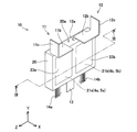
- FIG. 2 shows a perspective view of the semiconductor module 10.
- FIG. 3 shows a cross section taken along the line III-III of FIG.
- the main body of the semiconductor module 10 is a resin package 20, and two semiconductor chips 21a and 21b are embedded in the package 20.
- a parallel circuit of the switching element 4a and the diode 5a of FIG. 1 is mounted on the semiconductor chip 21a, and a parallel circuit of the switching element 4b and the diode 5b of FIG. 1 is mounted on the semiconductor chip 21b.
- the semiconductor chips 21a and 21b are flat plates, and electrodes are exposed on both sides of the wide surface thereof.
- a spacer 24a is bonded to the positive electrode of the semiconductor chip 21a (the positive electrode of the switching element 4a), and a metal plate 23a is bonded to the opposite side of the spacer 24a.
- the negative electrode of the semiconductor chip 21a (the negative electrode of the switching element 4a) is bonded to the metal plate 22, and the positive electrode of the semiconductor chip 21b (the positive electrode of the switching element 4b) is bonded to the metal plate 22. That is, the metal plate 22 connects the two switching elements 4a and 4b in series.
- the negative electrode of the semiconductor chip 21b (the negative electrode of the switching element 4b) is bonded to the spacer 24b, and the metal plate 23b is bonded to the opposite side of the spacer 24b.
- the metal plate 23a corresponds to the high potential side of the series connection circuit of the two switching elements 4a and 4b, and the metal plate 23b corresponds to the low potential side of the series connection circuit.
- One surface of the metal plates 22, 23a, 23b is exposed from the package 20, and the heat of the semiconductor chips 21a, 21b is released.
- the package 20 is flat, and the positive electrode terminal 11 and the negative electrode terminal 12 are provided on a narrow surface 20a facing the + Y direction of the coordinate system in the drawing.
- the negative electrode terminal 12 has a base portion 12a extending in the Y direction from the first narrow surface 20a, an intermediate portion 12b bent at a right angle in the X direction from the base portion 12a, and a base portion 12b bent at a right angle in the Y direction from the intermediate portion 12b. It has a tip portion 12c.
- the base portion 11a of the positive electrode terminal 11 is hidden behind the intermediate portion 11b and cannot be seen.
- the base portion 11a (12a), the intermediate portion 11b (12b), and the tip portion 11c (12c) are flat plates, respectively.
- the midpoint terminal 13 and the control terminals 14a and 14b are provided on the narrow surface 20b facing the ⁇ Y direction on the opposite side.
- the surface 20a of the package 20 facing the + Y direction is hereinafter referred to as the first narrow surface 20a
- the surface 20b facing the ⁇ Y direction is referred to as the second narrow surface 20b.
- the positive electrode terminal 11 and the negative electrode terminal 12 are connected to the metal plates 23a and 23b inside the package 20, respectively.
- the midpoint terminal 13 is connected to the metal plate 22 inside the package 20.
- the positive electrode terminal 11, the negative electrode terminal 12, and the midpoint terminal 13 are on the high potential side of the series connection circuit of the two semiconductor chips 21a and 21b (two switching elements 4a and 4b) via the metal plates 22, 23a and 23b. , Conducts with the low potential side and the midpoint.
- the positive electrode terminal 11 is connected to the positive electrode of the switching element 4a
- the negative electrode terminal 12 is connected to the negative electrode of the switching element 4b.
- the control terminal 14a (14b) is connected to a control pad (not shown) of the semiconductor chip 21a (21b).
- the control pad is composed of a gate of a switching element, a terminal of a temperature sensor (not shown), and the like.
- a drive signal is sent from the motor controller 6 to the switching element 4a (4b) via the control terminals 14a (14b).
- FIG. 4 shows a perspective view of the power converter 2.
- FIG. 4 is a perspective view of the assembly of the semiconductor module 10 and the capacitor 3, which are the main components of the power converter 2. In FIG. 4, parts other than the assembly (including the housing) are not shown.
- FIG. 5 shows a perspective view of the power converter 2 in a state where the capacitor 3 is removed from the semiconductor module 10.
- the power converter 2 includes three semiconductor modules 10 (10a-10c), four coolers 30 (30a-30d), and a capacitor 3.
- Reference numeral 30 is used when the four coolers 30 are collectively referred to, and reference numerals 30a-30d are used when the four coolers 30 are individually represented.
- the three semiconductor modules 10 and the four coolers 30 are alternately laminated one by one.
- the plurality of semiconductor modules 10 and the plurality of coolers 30 are arranged in the X direction of the coordinate system in the drawing.
- Each semiconductor module 10 will be sandwiched between a pair of coolers.
- the semiconductor module 10a is sandwiched between a pair of coolers 30a and 30b.
- the semiconductor module 10b is sandwiched between a pair of coolers 30b and 30c.
- the semiconductor module 10c is sandwiched between a pair of coolers 30c and 30d.
- Refrigerant passes through the inside of the cooler 30.
- the refrigerant is a liquid.
- the adjacent coolers 30 are connected by a pair of connecting pipes 31a and 31b.
- the connecting pipes 31a and 31b connect the flow paths in the adjacent coolers 30.
- the cooler 30d at the right end of the figure is provided with a refrigerant inlet 32a and a refrigerant outlet 32b.
- the refrigerant inlet 32a and the refrigerant outlet 32b are connected to a refrigerant circulation device (not shown).
- the refrigerant supplied from the refrigerant inlet 32a is distributed to all the coolers 30 through the connecting pipe 31a.
- the refrigerant absorbs heat from the adjacent semiconductor modules 10 while passing through the inside of the cooler 30.
- the heat-absorbed refrigerant is discharged from the refrigerant outlet 32b through the connecting pipe 31b. Since each semiconductor module 10 is cooled from both sides, the power converter 2 has a high cooling efficiency with respect to
- a positive electrode terminal 11 and a negative electrode terminal 12 are provided on the first narrow surface 20a of each semiconductor module 10.
- the first narrow surface 20a is a surface facing the Y direction of the coordinate system in the drawing, and the positive electrode terminal 11 and the negative electrode terminal 12 are arranged in the Z direction.
- the capacitor 3 is arranged so as to face the first narrow surface 20a of the semiconductor module 10.
- the capacitor 3 has electrodes (positive electrode 3p, negative electrode 3n) at both ends in the Z direction of the coordinate system in the drawing.
- the tip 11c of the positive electrode terminal 11 of the semiconductor module 10 and the tip 12c of the negative electrode terminal 12 sandwich the capacitor 3 in the Z direction, the tip 11c is joined to the positive electrode 3p of the capacitor 3, and the tip 12c is the negative electrode of the capacitor 3. It is joined to 3n.
- the circuit board 7 is arranged below the plurality of semiconductor modules 10.
- the motor controller 6 shown in FIG. 1 is mounted on the circuit board 7.
- FIG. 6 shows a front view of the power converter 2.
- Control terminals 14a and 14b and a midpoint terminal 13 are provided on the second narrow surface 20b of the semiconductor module 10.
- the circuit board 7 is arranged so as to face the second narrow surface 20b.
- the control terminals 14a and 14b are connected to the circuit board 7.
- the midpoint terminal 13 passes through the circuit board 7 and is joined to another bus bar.
- a bus bar is a conductive member made of a metal rod (metal plate).
- the capacitor 3 is arranged so as to face the first narrow surface 20a of the semiconductor module 10.
- a positive electrode terminal 11 and a negative electrode terminal 12 are provided on the first narrow surface 20a.
- the distance from the positive electrode terminal 11 (negative electrode terminal 12) to the capacitor 3 is short. Since the current path from the switching elements 4a and 4b inside the semiconductor module 10 to the capacitor 3 is short, the inductance generated in the current path can be suppressed. Inductance generated in the current path causes power loss.
- the power converter 2 having a short current path from the switching element to the capacitor has a small loss.
- Connecting pipes 31a and 31b are arranged on both sides of the semiconductor module 10 in the Z direction. Therefore, if the capacitors 3 are arranged adjacent to the semiconductor module 10 in the Z direction, the distance from the switching element in the semiconductor module 10 to the capacitor 3 becomes long.
- a plurality of semiconductor modules 10 and a plurality of coolers 30 are arranged in the X direction. Therefore, even if the capacitors 3 are arranged adjacent to the semiconductor module 10 in the X direction, the distance from the switching element in the semiconductor module 10 to the capacitor 3 becomes long.
- the capacitor 3 is arranged so as to be adjacent to the semiconductor module 10 in the Y direction. Such an arrangement can minimize the distance from the switching element in the semiconductor module 10 to the capacitor 3.
- the intermediate portion 11b of the positive electrode terminal 11 and the intermediate portion 12b of the negative electrode terminal 12 extend along the side surface of the capacitor 3 and extend in opposite directions along the Z axis.
- the tip 11c of the positive electrode terminal 11 and the tip 12c of the negative electrode 12 are bent so as to face each other, and the capacitor 3 is sandwiched between them. As described above, the tip 11c of the positive electrode terminal 11 is bonded to the positive electrode 3p of the capacitor 3, and the tip 12c of the negative electrode terminal 12 is bonded to the negative electrode 3n of the capacitor 3.
- the capacitor 3 is arranged so that the center line CL in the Z direction (the direction in which the positive electrode terminal 11 and the negative electrode terminal 12 are arranged) passes between the positive electrode terminal 11 and the negative electrode terminal 12. Then, the positive electrode terminal 11 and the negative electrode terminal 12 extend in opposite directions along the side surface of the capacitor 3. With this configuration, a current flows as shown by the thick arrow line in FIG. In particular, high-frequency noise flows along the surface layer of the capacitor 3. That is, the current flowing through the positive electrode terminal 11 and the negative electrode terminal 12 and the current flowing inside the capacitor 3 are close to each other.
- FIG. 7 shows a front view of the power converter 102 of the modified example.
- the positive electrode terminal 11 and the negative electrode terminal 12 are provided on the first narrow surface 20a
- the midpoint terminal 13 is provided on the second narrow surface 20b on the opposite side.
- the semiconductor module 110 used in the power converter 102 of the modified example is provided with a positive electrode terminal 111, a negative electrode terminal 112, and a midpoint terminal 113 on the first narrow surface 20a of the package 20.
- the positive electrode terminal 111, the negative electrode terminal 112, and the midpoint terminal 113 are arranged in the Z direction on the first narrow surface 20a.
- a midpoint terminal 113 is also provided on the first narrow surface 20a, and the space between the positive electrode terminal 111 and the negative electrode terminal 112 is narrowed. Nevertheless, the positive electrode terminal 111 and the negative electrode terminal 112 are arranged in the Z direction, and the capacitor 103 is arranged between them.
- the capacitor 103 is arranged so as to face the first narrow surface 20a.
- the capacitor 103 is arranged so that the center line CL of the capacitor 103 in the Z direction passes between the positive electrode terminal 111 and the negative electrode terminal 112.
- the positive electrode terminal 111 and the negative electrode terminal 112 extend in opposite directions along the side surface of the capacitor 103, the positive electrode terminal 111 is bonded to the positive electrode 3p of the capacitor 103, and the negative electrode terminal 112 is bonded to the negative electrode 3n. ..
- the power converter 102 of the modified example also has the same effect as the power converter 2 of the embodiment.
- FIG. 8 is a perspective view of the power converter 202
- FIG. 9 is an exploded perspective view of the power converter 202.
- the power converter 202 of the second embodiment uses the semiconductor module 10 (10a-10c) used by the power converter 2 of the first embodiment, but the arrangement thereof is different from that of the first embodiment.
- three semiconductor modules 10a-10c are sandwiched between a pair of coolers 230a and 230b.
- the three semiconductor modules 10a-10c are arranged in the Z direction of the coordinate system in the figure.
- the Z direction is the same as the arrangement direction of the positive electrode terminal 11 and the negative electrode terminal 12 in the semiconductor module 10.
- the positive electrode terminals 11 and the negative electrode terminals 12 of the three semiconductor modules 10a-10c are connected to one capacitor 3.
- the power converter 202 of the second embodiment has three capacitors 3a-3c, and each of the semiconductor modules 10a-10c is connected to each of the three capacitors 3a-3c.
- the power converter 202 is the same as the power converter 2 in other features except that the arrangement of the three semiconductor modules 10a-10c is different. Therefore, the power converter 2 of the second embodiment has the same advantages as the power converter 2 of the first embodiment.
- FIG. 10 shows a side view of the power converter 302 of the modified example.
- a housing 380 accommodating the coolers 330a and 330b, the semiconductor module 310, and the capacitor 3 is also drawn.
- FIG. 10 shows a cross section of the housing 380 of the power converter 302 cut by the XY plane of the coordinate system in the drawing. The side surfaces of the pair of coolers 330a and 330b, the semiconductor module 310, and the condenser 3 are drawn.
- the shape of the terminals of the semiconductor module 310 is slightly different from that of the semiconductor module 10.
- the power converter 302 also has three semiconductor modules 310 sandwiched between a pair of coolers 330a and 330b.
- the three semiconductor modules 310 are arranged in the Z direction, and the two semiconductor modules 310 are arranged on the back side of the paper in FIG.
- the pair of coolers 330a and 330b and the semiconductor module 310 are arranged in the X direction of the coordinate system in the figure, and the positive electrode terminal 311 and the negative electrode terminal of the respective semiconductor module 310 (in FIG. 10, the negative electrode terminal is hidden behind the positive electrode terminal 311).
- the capacitors 3 are arranged in the Z direction, the capacitors 3 face the first narrow surface 20a of the semiconductor module 310 in the Y direction, and the positive electrode terminal 311 and the negative electrode terminal (not shown in FIG. 1) are in the Z direction. A capacitor 3 is sandwiched between them.
- the circuit board 307 on which the motor controller 6 is mounted is arranged above the assembly of the coolers 330a and 330b and the semiconductor module 310.
- the circuit board 307 is fixed to the housing 380.
- the control terminal 314 of the semiconductor module 310 is bent upward and is connected to the circuit board 307.
- the midpoint terminal 313 is connected to one end of the intermediate bus bar 384.
- the other end of the intermediate bus bar 384 is connected to one end of the output bus bar 385.
- the output bus bar 385 extends out of the housing 380.
- the output bus bar 385 is connected to a traveling motor 92 (see FIG. 1).
- the circuit board 307 faces the cooler 330a with the heat transfer sheet 382 interposed therebetween.
- the heat transfer sheet 382 is shown in gray to aid understanding.
- the circuit board 307 is thermally connected to the cooler 330a.
- the arrow line from the circuit board 7 to the cooler 330a represents the heat flow. According to the structure of FIG. 10, the circuit board 7 is cooled by the cooler 330a.
- the lower surface of the capacitor 3 is in contact with the bottom plate 381 of the housing 380.
- the cooler 330b is also in contact with the bottom plate 381.
- the arrow line from the lower part of the condenser 3 to the bottom plate 381 and the arrow line from the bottom plate 381 to the cooler 330b also show the heat flow. As shown by those arrow lines, the condenser 3 is cooled by the cooler 330b.
- the capacitor 3 is arranged so as to face the first narrow surface on which the positive electrode terminal 11 and the negative electrode terminal 12 are provided.
- the capacitor is arranged so that the center line CL in the Z direction passes between the positive electrode terminal 11 and the negative electrode terminal 12.
- the capacitor 3 is provided with electrodes (positive electrode 3p and negative electrode 3n) at both ends in the Z direction.
- the positive electrode terminal 11 extends in the Z direction along the side surface of the capacitor 3, and the tip end portion 11c is connected to one electrode (for example, the positive electrode 3p) of the capacitor 3.
- the negative electrode terminal 12 extends along the side surface of the capacitor 3 in the direction opposite to that of the positive electrode terminal 11, and the tip portion 12c is connected to the other electrode (for example, the negative electrode 3n) of the capacitor 3.
- the current path from the switching elements 4a and 4b inside the semiconductor module 10 to the capacitor 3 is shortened, and the inductance generated in the current path can be suppressed. Further, a current flows in the opposite direction inside the positive electrode terminal 11 (negative electrode terminal 12) and the capacitor 3. This structure also contributes to the suppression of inductance.
- the semiconductor module 10 accommodates a series connection circuit of two switching elements 4a and 4b.
- the positive electrode terminal 11 is connected to the high potential side of the series connection circuit, and the negative electrode terminal 12 is connected to the low potential side of the series connection circuit.
- the midpoint terminal 13 connected to the midpoint of the series connection circuit extends from the second narrow surface on the opposite side of the first narrow surface.
- a plurality of coolers 30 are arranged in the X direction, and a plurality of semiconductor modules 10 and a plurality of coolers 30 are alternately laminated one by one along the X direction.
- the positive electrode terminal 11 and the negative electrode terminal 12 of each semiconductor module 10 are connected to the capacitor 3.
- a plurality of semiconductor modules 10 are arranged along the Z direction.
- a pair of coolers 230a and 230b sandwich a plurality of semiconductor modules 10a-10c.
- the X, Y, and Z directions in the figure correspond to the first, second, and third directions, respectively.
- the first narrow surface 20a corresponds to the first surface on which the positive electrode terminal 11 and the negative electrode terminal 12 are provided.
- both the first narrow surface 20a and the second narrow surface 20b are flat, but the first narrow surface 20a and the second narrow surface 20b do not have to be flat.
- the technology disclosed herein can be applied to a power converter in which at least one semiconductor module is sandwiched between a pair of coolers.
- the technology disclosed herein is not limited to the number of semiconductor modules and the number of coolers.
Landscapes
- Engineering & Computer Science (AREA)
- Power Engineering (AREA)
- Inverter Devices (AREA)
Priority Applications (2)
| Application Number | Priority Date | Filing Date | Title |
|---|---|---|---|
| PCT/JP2020/001996 WO2021149165A1 (ja) | 2020-01-21 | 2020-01-21 | 電力変換器 |
| JP2021572170A JP7136371B2 (ja) | 2020-01-21 | 2020-01-21 | 電力変換器 |
Applications Claiming Priority (1)
| Application Number | Priority Date | Filing Date | Title |
|---|---|---|---|
| PCT/JP2020/001996 WO2021149165A1 (ja) | 2020-01-21 | 2020-01-21 | 電力変換器 |
Publications (1)
| Publication Number | Publication Date |
|---|---|
| WO2021149165A1 true WO2021149165A1 (ja) | 2021-07-29 |
Family
ID=76993183
Family Applications (1)
| Application Number | Title | Priority Date | Filing Date |
|---|---|---|---|
| PCT/JP2020/001996 Ceased WO2021149165A1 (ja) | 2020-01-21 | 2020-01-21 | 電力変換器 |
Country Status (2)
| Country | Link |
|---|---|
| JP (1) | JP7136371B2 (https=) |
| WO (1) | WO2021149165A1 (https=) |
Citations (4)
| Publication number | Priority date | Publication date | Assignee | Title |
|---|---|---|---|---|
| JP2011114966A (ja) * | 2009-11-27 | 2011-06-09 | Denso Corp | 電力変換装置 |
| US20110242725A1 (en) * | 2008-10-08 | 2011-10-06 | Mtu Aero Engines Gmbh | Capacitor arrangement and method for producing a capacitor arrangement |
| JP2017163756A (ja) * | 2016-03-10 | 2017-09-14 | 株式会社デンソー | 電力変換装置 |
| JP2019097237A (ja) * | 2017-11-20 | 2019-06-20 | 株式会社デンソー | 電力変換装置 |
Family Cites Families (2)
| Publication number | Priority date | Publication date | Assignee | Title |
|---|---|---|---|---|
| JP5343928B2 (ja) | 2010-06-07 | 2013-11-13 | 株式会社デンソー | 電力変換装置 |
| WO2019244502A1 (ja) | 2018-06-19 | 2019-12-26 | 株式会社デンソー | 電力変換装置 |
-
2020
- 2020-01-21 WO PCT/JP2020/001996 patent/WO2021149165A1/ja not_active Ceased
- 2020-01-21 JP JP2021572170A patent/JP7136371B2/ja active Active
Patent Citations (4)
| Publication number | Priority date | Publication date | Assignee | Title |
|---|---|---|---|---|
| US20110242725A1 (en) * | 2008-10-08 | 2011-10-06 | Mtu Aero Engines Gmbh | Capacitor arrangement and method for producing a capacitor arrangement |
| JP2011114966A (ja) * | 2009-11-27 | 2011-06-09 | Denso Corp | 電力変換装置 |
| JP2017163756A (ja) * | 2016-03-10 | 2017-09-14 | 株式会社デンソー | 電力変換装置 |
| JP2019097237A (ja) * | 2017-11-20 | 2019-06-20 | 株式会社デンソー | 電力変換装置 |
Also Published As
| Publication number | Publication date |
|---|---|
| JPWO2021149165A1 (https=) | 2021-07-29 |
| JP7136371B2 (ja) | 2022-09-13 |
Similar Documents
| Publication | Publication Date | Title |
|---|---|---|
| US8686601B2 (en) | Power conversion apparatus for vehicle use | |
| JP7151599B2 (ja) | 電力変換器 | |
| JP2014090629A (ja) | 電力変換装置 | |
| JP7035845B2 (ja) | 電力変換装置 | |
| CN109873567B (zh) | 电力变换装置 | |
| JP2015139270A (ja) | 電力変換装置 | |
| JP2017005805A (ja) | 電力変換装置 | |
| US11916491B2 (en) | Electric power converter | |
| US12101036B2 (en) | Electric power converter | |
| JP7136371B2 (ja) | 電力変換器 | |
| JP6372433B2 (ja) | 電力変換装置 | |
| JP6943212B2 (ja) | 電力変換器 | |
| US12004333B2 (en) | Power converter | |
| JP2018060863A (ja) | 半導体積層ユニット | |
| JP7035543B2 (ja) | 電力変換器 | |
| JP2021111709A (ja) | 電力変換装置 | |
| JP7078182B2 (ja) | 電力変換器および電気自動車 | |
| JP7806716B2 (ja) | 電力変換装置 | |
| JP7092268B2 (ja) | 電力変換器 | |
| JP2020137134A (ja) | 電力変換器 |
Legal Events
| Date | Code | Title | Description |
|---|---|---|---|
| 121 | Ep: the epo has been informed by wipo that ep was designated in this application |
Ref document number: 20915553 Country of ref document: EP Kind code of ref document: A1 |
|
| ENP | Entry into the national phase |
Ref document number: 2021572170 Country of ref document: JP Kind code of ref document: A |
|
| NENP | Non-entry into the national phase |
Ref country code: DE |
|
| 122 | Ep: pct application non-entry in european phase |
Ref document number: 20915553 Country of ref document: EP Kind code of ref document: A1 |