WO2021140855A1 - フレキシブルプリント配線板及びその製造方法 - Google Patents
フレキシブルプリント配線板及びその製造方法 Download PDFInfo
- Publication number
- WO2021140855A1 WO2021140855A1 PCT/JP2020/046964 JP2020046964W WO2021140855A1 WO 2021140855 A1 WO2021140855 A1 WO 2021140855A1 JP 2020046964 W JP2020046964 W JP 2020046964W WO 2021140855 A1 WO2021140855 A1 WO 2021140855A1
- Authority
- WO
- WIPO (PCT)
- Prior art keywords
- layer
- winding
- winding portion
- plating
- average thickness
- Prior art date
- Legal status (The legal status is an assumption and is not a legal conclusion. Google has not performed a legal analysis and makes no representation as to the accuracy of the status listed.)
- Ceased
Links
Images




Classifications
-
- H—ELECTRICITY
- H05—ELECTRIC TECHNIQUES NOT OTHERWISE PROVIDED FOR
- H05K—PRINTED CIRCUITS; CASINGS OR CONSTRUCTIONAL DETAILS OF ELECTRIC APPARATUS; MANUFACTURE OF ASSEMBLAGES OF ELECTRICAL COMPONENTS
- H05K3/00—Apparatus or processes for manufacturing printed circuits
- H05K3/10—Apparatus or processes for manufacturing printed circuits in which conductive material is applied to the insulating support in such a manner as to form the desired conductive pattern
- H05K3/108—Apparatus or processes for manufacturing printed circuits in which conductive material is applied to the insulating support in such a manner as to form the desired conductive pattern by semi-additive methods; masks therefor
-
- C—CHEMISTRY; METALLURGY
- C25—ELECTROLYTIC OR ELECTROPHORETIC PROCESSES; APPARATUS THEREFOR
- C25D—PROCESSES FOR THE ELECTROLYTIC OR ELECTROPHORETIC PRODUCTION OF COATINGS; ELECTROFORMING; APPARATUS THEREFOR
- C25D5/00—Electroplating characterised by the process; Pretreatment or after-treatment of workpieces
- C25D5/02—Electroplating of selected surface areas
-
- C—CHEMISTRY; METALLURGY
- C25—ELECTROLYTIC OR ELECTROPHORETIC PROCESSES; APPARATUS THEREFOR
- C25D—PROCESSES FOR THE ELECTROLYTIC OR ELECTROPHORETIC PRODUCTION OF COATINGS; ELECTROFORMING; APPARATUS THEREFOR
- C25D7/00—Electroplating characterised by the article coated
-
- H—ELECTRICITY
- H01—ELECTRIC ELEMENTS
- H01F—MAGNETS; INDUCTANCES; TRANSFORMERS; SELECTION OF MATERIALS FOR THEIR MAGNETIC PROPERTIES
- H01F17/00—Fixed inductances of the signal type
-
- H—ELECTRICITY
- H01—ELECTRIC ELEMENTS
- H01F—MAGNETS; INDUCTANCES; TRANSFORMERS; SELECTION OF MATERIALS FOR THEIR MAGNETIC PROPERTIES
- H01F27/00—Details of transformers or inductances, in general
- H01F27/28—Coils; Windings; Conductive connections
-
- H—ELECTRICITY
- H01—ELECTRIC ELEMENTS
- H01F—MAGNETS; INDUCTANCES; TRANSFORMERS; SELECTION OF MATERIALS FOR THEIR MAGNETIC PROPERTIES
- H01F41/00—Apparatus or processes specially adapted for manufacturing or assembling magnets, inductances or transformers; Apparatus or processes specially adapted for manufacturing materials characterised by their magnetic properties
- H01F41/02—Apparatus or processes specially adapted for manufacturing or assembling magnets, inductances or transformers; Apparatus or processes specially adapted for manufacturing materials characterised by their magnetic properties for manufacturing cores, coils, or magnets
- H01F41/04—Apparatus or processes specially adapted for manufacturing or assembling magnets, inductances or transformers; Apparatus or processes specially adapted for manufacturing materials characterised by their magnetic properties for manufacturing cores, coils, or magnets for manufacturing coils
-
- H—ELECTRICITY
- H05—ELECTRIC TECHNIQUES NOT OTHERWISE PROVIDED FOR
- H05K—PRINTED CIRCUITS; CASINGS OR CONSTRUCTIONAL DETAILS OF ELECTRIC APPARATUS; MANUFACTURE OF ASSEMBLAGES OF ELECTRICAL COMPONENTS
- H05K1/00—Printed circuits
- H05K1/02—Details
- H05K1/0277—Bendability or stretchability details
- H05K1/028—Bending or folding regions of flexible printed circuits
-
- H—ELECTRICITY
- H05—ELECTRIC TECHNIQUES NOT OTHERWISE PROVIDED FOR
- H05K—PRINTED CIRCUITS; CASINGS OR CONSTRUCTIONAL DETAILS OF ELECTRIC APPARATUS; MANUFACTURE OF ASSEMBLAGES OF ELECTRICAL COMPONENTS
- H05K1/00—Printed circuits
- H05K1/02—Details
- H05K1/11—Printed elements for providing electric connections to or between printed circuits
- H05K1/115—Via connections; Lands around holes or via connections
- H05K1/116—Lands, clearance holes or other lay-out details concerning the surrounding of a via
-
- H—ELECTRICITY
- H05—ELECTRIC TECHNIQUES NOT OTHERWISE PROVIDED FOR
- H05K—PRINTED CIRCUITS; CASINGS OR CONSTRUCTIONAL DETAILS OF ELECTRIC APPARATUS; MANUFACTURE OF ASSEMBLAGES OF ELECTRICAL COMPONENTS
- H05K3/00—Apparatus or processes for manufacturing printed circuits
- H05K3/02—Apparatus or processes for manufacturing printed circuits in which the conductive material is applied to the surface of the insulating support and is thereafter removed from such areas of the surface which are not intended for current conducting or shielding
- H05K3/06—Apparatus or processes for manufacturing printed circuits in which the conductive material is applied to the surface of the insulating support and is thereafter removed from such areas of the surface which are not intended for current conducting or shielding the conductive material being removed chemically or electrolytically, e.g. by photo-etch process
- H05K3/061—Etching masks
-
- H—ELECTRICITY
- H05—ELECTRIC TECHNIQUES NOT OTHERWISE PROVIDED FOR
- H05K—PRINTED CIRCUITS; CASINGS OR CONSTRUCTIONAL DETAILS OF ELECTRIC APPARATUS; MANUFACTURE OF ASSEMBLAGES OF ELECTRICAL COMPONENTS
- H05K3/00—Apparatus or processes for manufacturing printed circuits
- H05K3/22—Secondary treatment of printed circuits
- H05K3/24—Reinforcing of the conductive pattern
- H05K3/241—Reinforcing of the conductive pattern characterised by the electroplating method; means therefor, e.g. baths or apparatus
-
- H—ELECTRICITY
- H05—ELECTRIC TECHNIQUES NOT OTHERWISE PROVIDED FOR
- H05K—PRINTED CIRCUITS; CASINGS OR CONSTRUCTIONAL DETAILS OF ELECTRIC APPARATUS; MANUFACTURE OF ASSEMBLAGES OF ELECTRICAL COMPONENTS
- H05K3/00—Apparatus or processes for manufacturing printed circuits
- H05K3/40—Forming printed elements for providing electric connections to or between printed circuits
- H05K3/4038—Through-connections; Vertical interconnect access [VIA] connections
-
- H—ELECTRICITY
- H05—ELECTRIC TECHNIQUES NOT OTHERWISE PROVIDED FOR
- H05K—PRINTED CIRCUITS; CASINGS OR CONSTRUCTIONAL DETAILS OF ELECTRIC APPARATUS; MANUFACTURE OF ASSEMBLAGES OF ELECTRICAL COMPONENTS
- H05K1/00—Printed circuits
- H05K1/02—Details
- H05K1/11—Printed elements for providing electric connections to or between printed circuits
- H05K1/115—Via connections; Lands around holes or via connections
-
- H—ELECTRICITY
- H05—ELECTRIC TECHNIQUES NOT OTHERWISE PROVIDED FOR
- H05K—PRINTED CIRCUITS; CASINGS OR CONSTRUCTIONAL DETAILS OF ELECTRIC APPARATUS; MANUFACTURE OF ASSEMBLAGES OF ELECTRICAL COMPONENTS
- H05K1/00—Printed circuits
- H05K1/16—Printed circuits incorporating printed electric components, e.g. printed resistors, capacitors or inductors
- H05K1/165—Printed circuits incorporating printed electric components, e.g. printed resistors, capacitors or inductors incorporating printed inductors
-
- H—ELECTRICITY
- H05—ELECTRIC TECHNIQUES NOT OTHERWISE PROVIDED FOR
- H05K—PRINTED CIRCUITS; CASINGS OR CONSTRUCTIONAL DETAILS OF ELECTRIC APPARATUS; MANUFACTURE OF ASSEMBLAGES OF ELECTRICAL COMPONENTS
- H05K2201/00—Indexing scheme relating to printed circuits covered by H05K1/00
- H05K2201/09—Shape and layout
- H05K2201/09209—Shape and layout details of conductors
- H05K2201/09654—Shape and layout details of conductors covering at least two types of conductors provided for in H05K2201/09218 - H05K2201/095
- H05K2201/09736—Varying thickness of a single conductor; Conductors in the same plane having different thicknesses
-
- H—ELECTRICITY
- H05—ELECTRIC TECHNIQUES NOT OTHERWISE PROVIDED FOR
- H05K—PRINTED CIRCUITS; CASINGS OR CONSTRUCTIONAL DETAILS OF ELECTRIC APPARATUS; MANUFACTURE OF ASSEMBLAGES OF ELECTRICAL COMPONENTS
- H05K2201/00—Indexing scheme relating to printed circuits covered by H05K1/00
- H05K2201/09—Shape and layout
- H05K2201/09209—Shape and layout details of conductors
- H05K2201/09654—Shape and layout details of conductors covering at least two types of conductors provided for in H05K2201/09218 - H05K2201/095
- H05K2201/09781—Dummy conductors, i.e. not used for normal transport of current; Dummy electrodes of components
-
- H—ELECTRICITY
- H05—ELECTRIC TECHNIQUES NOT OTHERWISE PROVIDED FOR
- H05K—PRINTED CIRCUITS; CASINGS OR CONSTRUCTIONAL DETAILS OF ELECTRIC APPARATUS; MANUFACTURE OF ASSEMBLAGES OF ELECTRICAL COMPONENTS
- H05K2201/00—Indexing scheme relating to printed circuits covered by H05K1/00
- H05K2201/09—Shape and layout
- H05K2201/09818—Shape or layout details not covered by a single group of H05K2201/09009 - H05K2201/09809
- H05K2201/09981—Metallised walls
-
- H—ELECTRICITY
- H05—ELECTRIC TECHNIQUES NOT OTHERWISE PROVIDED FOR
- H05K—PRINTED CIRCUITS; CASINGS OR CONSTRUCTIONAL DETAILS OF ELECTRIC APPARATUS; MANUFACTURE OF ASSEMBLAGES OF ELECTRICAL COMPONENTS
- H05K2203/00—Indexing scheme relating to apparatus or processes for manufacturing printed circuits covered by H05K3/00
- H05K2203/07—Treatments involving liquids, e.g. plating, rinsing
- H05K2203/0703—Plating
- H05K2203/0723—Electroplating, e.g. finish plating
-
- H—ELECTRICITY
- H05—ELECTRIC TECHNIQUES NOT OTHERWISE PROVIDED FOR
- H05K—PRINTED CIRCUITS; CASINGS OR CONSTRUCTIONAL DETAILS OF ELECTRIC APPARATUS; MANUFACTURE OF ASSEMBLAGES OF ELECTRICAL COMPONENTS
- H05K3/00—Apparatus or processes for manufacturing printed circuits
- H05K3/22—Secondary treatment of printed circuits
- H05K3/24—Reinforcing of the conductive pattern
- H05K3/243—Reinforcing of the conductive pattern characterised by selective plating, e.g. for finish plating of pads
Definitions
- This disclosure relates to a flexible printed wiring board and a method for manufacturing the same.
- the flexible printed wiring board is a flexible printed wiring board including a base film having holes for forming through holes and a coil-shaped wiring layer laminated on at least one surface side of the base film.
- the wiring layer has a land portion arranged on the inner peripheral surface of the hole and the peripheral edge portion of the hole in the base film, and the land portion has a spiral shape as an inner end portion or an outer end portion. It has a winding portion to be arranged, and the winding portion has a first winding portion which is the outermost peripheral portion and a second winding portion which is inside the outermost peripheral portion.
- the ratio of the average thickness of the land portion to the average thickness of the two winding portions is 1.1 or more and 5 or less.
- a method for manufacturing a flexible printed wiring board includes a base film having holes for forming through holes and a coil-shaped wiring layer laminated on at least one surface side of the base film.
- the wiring layer is a flexible printed wiring board comprising the land portion arranged on the inner peripheral surface of the hole and the peripheral portion of the hole in the base film, and the land portion is used as an inner end portion or an outer end portion.
- the winding portion has a winding portion arranged in a spiral shape, and the winding portion has a first winding portion which is the outermost circumference and a second winding portion which is inside the outermost circumference.
- the base film has a ratio of the average thickness of the land portion to the average thickness of the second winding portion of 1.1 or more and 5 or less, and has holes for forming through holes using a resist pattern.
- the second metal material is electroplated on the first plating body to have a second plating body having an upper land layer of the land portion and an upper winding layer of the winding portion.
- the amount of the second plating for forming the lower land layer is to form the inner side of the lowermost winding layer than the outermost circumference.
- the first metal material is electroplated on the conductive base layer so as to be larger than the first plating amount, and the land portion is formed by a part of the conductive base layer, the lower land layer, and the upper land layer.
- the winding portion is formed by another part of the conductive base layer, the lower winding layer, and the upper winding layer.
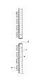
- FIG. 1 is a schematic top view showing a flexible printed wiring board of the first embodiment.
- FIG. 2 is a schematic end view showing the flexible printed wiring board of FIG.
- FIG. 3 is a schematic end view for explaining the manufacturing method of the flexible printed wiring board of FIGS. 1 and 2, and is a schematic end view viewed in the same direction as the direction of arrow AA in FIG.
- FIG. 4 is a schematic end view for explaining the manufacturing method of the flexible printed wiring board of FIGS. 1 and 2, and is a schematic end view viewed in the same direction as the AA arrow viewing direction of FIG.
- FIG. 5 is a schematic end view for explaining the manufacturing method of the flexible printed wiring board of FIGS. 1 and 2, and is a schematic end view viewed in the same direction as the AA arrow viewing direction of FIG.
- the flexible printed wiring board if conduction failure occurs or the electrical resistance is too large, connection failure may occur. Therefore, the flexible printed wiring board is required to have excellent connection reliability.
- the flexible printed wiring board according to one aspect of the present disclosure is excellent in connection reliability.
- the method for manufacturing a flexible printed wiring board according to another aspect of the present disclosure can manufacture a flexible printed wiring board having excellent connection reliability.
- the flexible printed wiring board according to one aspect of the present disclosure is a flexible printed wiring board including a base film having holes for forming through holes and a coil-shaped wiring layer laminated on at least one surface side of the base film.
- the wiring layer has a land portion arranged on the inner peripheral surface of the hole and the peripheral edge portion of the hole in the base film, and the land portion has a spiral shape as an inner end portion or an outer end portion.
- winding portion to be arranged, and the winding portion has a first winding portion which is the outermost peripheral portion and a second winding portion which is inside the outermost peripheral portion.
- the ratio of the average thickness of the land portion to the average thickness of the two winding portions is 1.1 or more and 5 or less.
- the flexible printed wiring board when the ratio is within the above range, the average thickness of the land portion is sufficiently large, and the amount of metal laminated on the inner peripheral surface of the hole is also large. can do. Therefore, it is possible to reduce the conduction failure in the through hole. Therefore, the flexible printed wiring board is excellent in connection reliability.
- the ratio of the average thickness of the first winding portion to the average thickness of the second winding portion is preferably 1.1 or more and 5 or less.
- the average thickness of the first winding portion on the outermost circumference is sufficiently large, and the electric resistance of the first winding portion can be reduced. Therefore, the electrical resistance of the wiring layer can be reduced.
- the flexible printed wiring board may further include one or a plurality of dummy wiring layers arranged at intervals from the wiring layer in the outer region of the wiring layer in the base film.
- the flexible printed wiring board By providing the flexible printed wiring board with a dummy wiring layer in this way, it becomes easy to form a wiring layer having a large average thickness of the first winding portion on the outermost circumference. Therefore, the flexible printed wiring board has more excellent connection reliability.
- the ratio of the second area of the laminated region of the dummy wiring layer to the first area of the region between the wiring layer and the outer side of the base film up to 2 mm at the shortest distance is 20% or more and less than 50%.
- the flexible printed wiring board has more excellent connection reliability.
- a base film having holes for forming through holes and a coil-shaped wiring layer laminated on at least one surface side of the base film are used.
- a flexible printed wiring board comprising the above, the wiring layer includes a land portion arranged on the inner peripheral surface of the hole and the peripheral edge portion of the hole in the base film, and the land portion at the inner end portion or the outer end portion. It has a winding portion arranged in a spiral shape as a portion, and the winding portion has a first winding portion which is the outermost peripheral portion and a second winding portion which is inside the outermost peripheral portion.
- the second metal material is electroplated on the first plating body to have a second plating having an upper land layer of the land portion and an upper winding layer of the winding portion.
- a second plating step for forming the body is provided, and in the first plating step, the amount of the second plating for forming the lower land layer is formed inside the outermost periphery of the lower winding layer.
- the first metal material is electroplated on the conductive base layer so as to be larger than the first plating amount of the above, and the land portion is formed by a part of the conductive base layer layer, the lower land layer and the upper land layer. Is formed, and the winding portion is formed by another part of the conductive base layer, the lower winding layer, and the upper winding layer.
- the above-mentioned flexible printed wiring board can be manufactured. That is, it is possible to manufacture a flexible printed wiring board having excellent connection reliability.
- the flexible printed wiring board further includes a dummy wiring layer arranged in an outer region of the wiring layer in the base film at intervals from the wiring layer, and is placed on the conductive base layer in the first plating step.
- a dummy plating body was formed, and was electrically isolated by the land portion and a part of the non-laminated region of the winding portion in the conductive base layer, and the dummy plating body. It is preferable that the dummy wiring layer is formed.
- the dummy plated body in the first plating step By forming the dummy plated body in the first plating step in this way, it becomes easy to form a wiring layer having a large average thickness of the first winding portion on the outermost circumference. Therefore, according to the method for manufacturing the flexible printed wiring board, it is possible to manufacture the flexible printed wiring board having more excellent connection reliability.
- the "outermost circumference of the winding portion” means a portion where only the inside faces the other portion of the winding portion.
- the “average thickness” means each average value of the thickness measured at an arbitrary ten points for each of the land, the first winding portion, and the second winding portion.
- Thiickness means the distance between the base film and the upper edge of the wiring layer in the direction perpendicular to the base film.
- the “line width” means the dimension of the winding portion in the direction perpendicular to the longitudinal direction (winding direction).
- the "spacing” means the distance between the adjacent adjacent surfaces in the winding portion, and the “average spacing” means the value obtained by averaging the distances between the adjacent surfaces in the longitudinal direction.
- the "average line width” means a value obtained by averaging the maximum width of the winding portion in the cross section perpendicular to the longitudinal direction in the longitudinal direction.
- the flexible printed wiring board 10 of the present embodiment has an insulating base film 3 and a wiring layer 11 laminated on one surface side (front surface side) of the base film 3. Mainly equipped with.
- the flexible printed wiring board 10 further includes a dummy wiring layer 31 arranged in the outer region of the wiring layer 11 in the base film 3 at intervals from the wiring layer 11.
- the flexible printed wiring board 10 may further include a cover film on the surface side of the base film 3 or the wiring layer 11.
- ⁇ Base film> The base film 3 is a layer made of a synthetic resin having an insulating property.
- the base film 3 also has flexibility.
- the base film 3 is also a base material for forming the wiring layer 11.
- the base film 3 has holes 3a for forming the through holes 20, and the material for forming the base film 3 is not particularly limited as long as it has insulating properties and flexibility, but is formed in a sheet shape.
- a synthetic resin film having a low dielectric constant can be adopted.
- the main component of this synthetic resin film include polyimide, polyethylene terephthalate, liquid crystal polymer, and fluororesin.
- the "main component” is a component having the highest content, and means, for example, a component that occupies 50% by mass or more in the forming material.
- the base film 3 may contain a resin other than the exemplified resin such as polyimide, an antistatic agent, and the like.
- the lower limit of the average thickness of the base film 3 is not particularly limited, but is preferably 3 ⁇ m, preferably 5 ⁇ m, and more preferably 10 ⁇ m.
- the upper limit of the average thickness of the base film 3 is not particularly limited, but is preferably 200 ⁇ m, more preferably 150 ⁇ m, and even more preferably 100 ⁇ m. If the average thickness of the base film 3 is less than the above lower limit, the dielectric strength and mechanical strength of the base film 3 may be insufficient. On the other hand, when the average thickness of the base film 3 exceeds the above upper limit, the flexible printed wiring board 10 may become unnecessarily thick.
- the "average thickness" means the average value of the thickness measured at any ten points.
- the through holes 20 can be formed in an appropriate place and in an appropriate size.
- the wiring layer 11 is laminated directly on the surface side of the base film 3 or via another layer.
- the wiring layer 11 has a coil shape.
- the wiring layer 11 has a land portion 13 arranged on the inner peripheral surface of the hole 3a for forming the through hole 20 and a peripheral portion of the hole 3a in the base film 3, and the land portion 13 is used as an inner end portion.
- It has a winding portion 15 arranged in a spiral shape.
- the winding portion 15 has a first winding portion 15a which is the outermost circumference and a second winding portion 15b which is inside the outermost circumference.
- the ratio of the average thickness H2 of the land portion to the average thickness H1 of the second winding portion 15b is 1.1 or more and 5 or less.
- the ratio of the average thickness H3 of the first winding portion 15a to the average thickness H1 of the second winding portion 15b is not particularly limited. For example, in the present embodiment, this ratio is 1.1 or more and 5 or less.
- the wiring layer 11 may have the land portion 13 as the outer end portion. Further, the wiring layer 11 may have two land portions as an inner end portion and an outer end portion, respectively.
- the land portion 13 is a dummy plating layer laminated on the side (surface side) opposite to the base film 3 of the first conductive base layer 23 and the first conductive base layer 23 laminated on the surface side of the base film 3. Formed by 25 and.
- the first conductive base layer 23 is also laminated on the inner peripheral surface of the hole 3a.
- the winding portion 15 is a lower layer winding laminated on the side (surface side) opposite to the base film 3 of the first conductive base layer 23 and the second conductive base layer 33 laminated on the surface side of the base film 3. It is formed by a wire layer 35 and an upper winding layer 37 laminated on the side (surface side) opposite to the second conductive base layer 33 of the lower winding portion 35.
- the average thickness of the region forming a part of the land portion 13 and the average thickness of the region forming a part of the first winding portion 15a of the upper winding portion 37 are the upper windings. It is formed so as to be larger than the average thickness of the region forming a part of the second winding portion 15b in the portion 37.
- Examples of the wiring layer 11 include a coil wire for sending a current for generating a magnetic field.
- the material for forming the first conductive base layer 23 and the second conductive base layer 33 examples include copper (Cu), silver (Ag), gold (Au), nickel (Ni), titanium (Ti), and chromium (Cr). ), These alloys, stainless steel and the like.
- the first conductive base layer 23 and the second conductive base layer 33 are different from the base film 3 (for example, polyimide) in that the thermal deterioration of the adhesion of the wiring layer 11 to the base film 3 is suppressed.
- the contacting side includes a layer (first layer) containing at least one selected from the group consisting of nickel, chromium, titanium and silver.
- first conductive base layer 23 and the second conductive base layer 33 contain at least one selected from nickel and chromium, which are easy to remove and easily maintain insulation (first layer). It is more preferable to include. Further, the first conductive base layer 23 and the second conductive base layer 33 have a copper-based layer (second layer) on the upper side of the first inner layer (the side opposite to the base film 3). It is more preferable to include it. By arranging the layer containing copper as a main component, it is possible to shorten the work time when forming the wiring layer 11 by electroplating.
- the lower limit of the average thickness of the first layer 1 nm is preferable, and 2 nm is more preferable.
- the upper limit of the average thickness of the first layer is preferably 15 nm, more preferably 8 nm. If the average thickness is less than the lower limit, it may be difficult to suppress thermal deterioration of the adhesion of the wiring layer 11 to the base film 3. On the other hand, when the average thickness exceeds the upper limit, the first layer is difficult to be easily removed, and the insulation of the wiring layer 11 may not be sufficiently maintained.
- the first layer can be formed by a sputtering method, an electroplating method, an electroless plating method, or the like.
- the lower limit of the average thickness of the second layer 0.1 ⁇ m is preferable, and 0.2 ⁇ m is more preferable.
- the upper limit of the average thickness of the second layer 2 ⁇ m is preferable, and 1 ⁇ m is more preferable. If the average thickness is less than the lower limit, the time for forming the wiring 11 by electroplating may become excessively long. On the other hand, when the average thickness exceeds the upper limit, the second layer is difficult to be easily removed, and the insulating property between the winding portions 15 may not be sufficiently maintained.
- the second layer is preferably formed by a sputtering method, an electroplating method, an electroless plating method, or the like, and may be formed by combining these.
- the electroless copper plating layer is arranged on the uppermost surface side of the first conductive base layer 23 and the second conductive base layer 33, whereby the inner layer is formed by the sputtering method.
- the inner layer is formed by the sputtering method.
- Examples of the first metal material for forming the lower land layer 25 and the lower winding layer 35 include copper, aluminum, silver, gold, nickel, and alloys thereof. Among these, copper or a copper alloy is preferable from the viewpoint of improving the conductivity and reducing the cost.
- the lower land layer 25 and the lower winding layer 35 are formed in the same shape as the first conductive base layer 23 and the second conductive base layer 33 when viewed in a direction perpendicular to the base film 3.
- Examples of the second metal material for forming the upper land layer 27 and the upper winding layer 37 include the same materials as those of the first metal material.
- the second metal material is preferably the same type as the first metal material.
- the upper land layer 27 and the upper winding layer 37 are formed so as to have a line width larger than the line width of the lower land layer 25 and the lower winding portion 35 when viewed in the direction perpendicular to the base film 3. (Land section)
- the average thickness H2 of the land portion 13 can be appropriately set so that the ratio of the average thickness H2 of the land portion 13 to the average thickness H1 of the second winding portion 15b described above is 1.1 or more and 10 or less.
- the lower limit of the average thickness H2 of the land portion 13 5 ⁇ m is preferable, 10 ⁇ m is more preferable, and 20 ⁇ m is further preferable.
- the upper limit of the average thickness H2 of the land portion 13 is preferably 100 ⁇ m, more preferably 75 ⁇ m, and even more preferably 50 ⁇ m. If the average thickness H2 is less than the upper limit, it may be difficult to attach the first metal material and the second metal material to the inner peripheral surface of the hole 3a in a sufficient amount (coating amount). is there. On the other hand, when the average thickness H2 exceeds the upper limit, the amount of adhesion of the first metal material and the second metal material to the inner peripheral surface of the hole 3a may become excessively large.
- the average thickness H2 is obtained by exposing the cross section of the wiring plate 10 with a cross-section processing device such as a microtome, measuring the thickness of the land portion 13 by observing the cross section of any ten points, and calculating the average value of the measurement results. can get.
- the maximum line width of the land portion 13, the ratio (aspect ratio) of the average thickness H2 to the maximum line width, and the like can be appropriately set.
- the lower limit of the average line width L of the winding portion 15 5 ⁇ m is preferable, 10 ⁇ m is more preferable, and 15 ⁇ m is further preferable.
- the upper limit of the average line width L of the winding portion 15 is preferably 100 ⁇ m, more preferably 75 ⁇ m, and even more preferably 50 ⁇ m. If the average line width L of the winding portion 15 is less than the above lower limit, the electrical resistance of the winding portion 15 may become too large or the mechanical strength may be insufficient.
- the "average line width” is obtained by exposing the cross section of the wiring plate 10 with a cross-section processing device such as a microtome, measuring the length of the widest portion of the winding portion 15 with a measurable microscope or the like, and averaging them. It is a value calculated as.
- the lower limit of the average interval S of the winding portions 15 5 ⁇ m is preferable, 10 ⁇ m is more preferable, and 15 ⁇ m is even more preferable.
- the upper limit of the average interval S of the winding portions 15 is preferably 50 ⁇ m, more preferably 50 ⁇ m, and even more preferably 25 ⁇ m. If the average interval S of the winding portions 15 is less than the above lower limit, a short circuit may occur. On the other hand, if the average interval S of the winding portions 15 exceeds the above upper limit, it may not be possible to save space.
- the "average spacing" is determined by exposing the cross section of the wiring plate 10 with a cross-section processing device such as a microtome, measuring the length of the smallest spacing in the gap between the winding portions 15 with a microscope or the like capable of measuring them. It is a value calculated as an average value of.
- the lower winding layer 35 and the upper winding layer 37 are much thicker than the second conductive base layer 33. Therefore, the thickness of the winding portion 15 can be determined mainly by the thickness of the lower winding layer 35 and the upper winding layer 37.
- the average thickness H1 of the inner second winding portion 15b in the second winding portion 15b is the average thickness H2 of the land portion 13 and the first outermost circumference with respect to the average thickness H1 of the second winding portion 15b.
- the ratio of the average thickness H3 of the winding portion 15a can be appropriately set to be 1.1 or more and 5 or less.
- the lower limit of the average thickness H1 of the second winding portion 15b 10 ⁇ m is preferable, 15 ⁇ m is more preferable, and 20 ⁇ m is further preferable.
- the upper limit of the average thickness H1 of the second winding portion 15b is preferably 100 ⁇ m, more preferably 80 ⁇ m, and even more preferably 60 ⁇ m. If the average thickness H1 is less than the upper limit, the electrical resistance of the second winding portion 15b may increase. On the other hand, when the average thickness H1 exceeds the upper limit, it is necessary to increase the line width in order to form the second winding portion 15b, and there is a possibility that space saving cannot be achieved.
- the "average thickness” is obtained by exposing the cross section of the wiring plate 10 with a cross-section processing device such as a microtome, measuring the thickness of the second winding portion 15 by observing the cross section of any ten points, and calculating the average value of the measurement results. Obtained by calculation.
- the "average thickness” of other members and the like is also a value measured in the same manner.
- the lower limit of the ratio (aspect ratio) of the average thickness H1 to the minimum line width (not shown) of the second winding portion 15b is preferably 0.3, preferably 0.5, and more preferably 0.7.
- As the upper limit of the ratio 5 is preferable, 3 is more preferable, and 2 is further preferable. If the above ratio is less than the above lower limit, it may not be possible to save space. On the other hand, even if the above ratio exceeds the above upper limit, it may not be possible to save space.
- the "minimum line width" means the minimum value of the line width in the second winding portion 15b.
- This "minimum line width” is measured by a microscope or the like capable of exposing the cross section of the wiring plate 10 with a cross-section processing device such as a microtome and measuring the length of the narrowest portion of the second winding portion 15b. The value.
- this "minimum line width” is the length of the narrowest portion in the region excluding the defect region of the second winding portion 15b.
- the defective region to be excluded from the measurement is a region that is recessed (defective) inward from at least one edge in the width direction when the microscope observation is performed as described above.
- the deepest portion in the width direction of this defect region is 1/4 of the average line width of other regions (other than the defect region) in the longitudinal direction (winding direction) of the second winding portion 15b. It is a region having the above length (width).
- the average line width is measured in the same manner as the above-mentioned "average line width” measuring method. It is a value measured by. In the following, the "minimum line width" of other members and the like is also a value measured in the same manner.
- the average thickness H3 of the first winding portion 15a on the outermost circumference of the first winding portion is such that the ratio of the average thickness H3 of the first winding portion 15a to the average thickness H1 of the second winding portion 15b described above is 1.1.
- the average thickness H3 of the first winding portion 15a 10 ⁇ m is preferable, 20 ⁇ m is more preferable, and 30 ⁇ m is further preferable.
- the upper limit of the average thickness H3 of the first winding portion 15a is preferably 120 ⁇ m, more preferably 100 ⁇ m, and even more preferably 80 ⁇ m. If the average thickness H3 is less than the upper limit, the electrical resistance of the first winding portion 15a may increase. On the other hand, when the average thickness H3 exceeds the upper limit, it is necessary to increase the line width in order to form the first winding portion 15a, and there is a possibility that space saving cannot be achieved.
- the lower limit of the ratio (aspect ratio) of the average thickness H3 to the minimum line width (not shown) of the first winding portion 15a is preferably 0.5, preferably 0.7, and more preferably 1.
- the lower limit of the ratio of the average thickness H2 of the land portion 13 to the average thickness H1 of the second winding portion 15b is 1.1, more preferably 1.3, more preferably 1.5, and 2 Is even more preferable.
- the upper limit of the ratio is 5, as described above, more preferably 4, and even more preferably 3. If the above ratio is less than the above lower limit, it may be difficult to attach the first metal material and the second metal material to the inner peripheral surface of the hole 3a in a sufficient amount (covering amount).
- the lower limit of the ratio of the average thickness H3 of the first winding portion 15a to the average thickness H1 of the second winding portion 15b is 1.1, more preferably 1.3, and 1.5. More preferably, 2 is even more preferable.
- the upper limit of the ratio is 5, as described above, more preferably 4, and even more preferably 3.
- the dummy wiring layer 41 is a wiring layer formed so as to be electrically isolated so as not to be conducted.
- the dummy wiring layer 41 has a third conductive base layer 43 and a dummy plating layer 45 laminated on the third conductive base layer 43.
- the average thickness H3 of the outermost first winding portion 15a of the winding portion 15 located in the vicinity of the dummy wiring layer 41 is increased. It will be easier to do. Specifically, when forming the upper winding portion 37, the amount of plating on the outermost periphery located in the vicinity of the dummy wiring layer 41 can be made larger than that on the inside. Therefore, it becomes easy to form the flexible printed wiring board 10 having more excellent connection reliability.
- the third conductive base layer 43 is formed by a part of the conductive base layer M (see, for example, FIG. 3) described later.
- Examples of the third conductive base layer 43 include those similar to the first conductive base layer 23 and the second conductive base layer 33.
- the average thickness of the third conductive base layer 43 can be set in the same manner as in the first conductive base layer 23 and the second conductive base layer 33.
- Examples of the material for forming the dummy plating layer 45 include the same materials as those of the first metal material described above.
- the thickness of the dummy wiring layer 41 can be determined by the thickness of the dummy plating layer 45.
- the average thickness of the dummy wiring layer 41 can be set to be about the same as the average thickness of the lower land layer 25 and the lower winding layer 35 described above.
- the laminated area of the dummy wiring layer 41 in the base film 3 can be appropriately set. For example, 20% is preferable as the lower limit of the ratio of the second area of the laminated region of the dummy wiring layer 41 to the first area of the region between the wiring portion 11 and the outer side of the base film 3 at the shortest distance of 2 mm. 25% is more preferable.
- the upper limit of the above ratio is preferably less than 50%, more preferably 40%. If the ratio is less than the lower limit, the electrical resistance of the wiring layer 11 may not be sufficiently reduced. On the other hand, even when the ratio exceeds the upper limit, the electrical resistance of the wiring layer 11 may not be sufficiently reduced. In addition, poor continuity may not be sufficiently reduced.
- the shape of the dummy wiring layer 41 is not particularly limited and may be appropriately set.
- the dummy wiring layer 41 can be set to a linear shape, another shape, or the like when viewed in a direction perpendicular to the base film 3.
- This shape can be appropriately set to, for example, a shape that satisfies the above area ratio.
- the dummy wiring layer 41 has a plurality of linear bodies. ⁇ Advantage> In the flexible printed wiring board 10, the ratio of the average thickness H2 of the land portion 13 to the average thickness H1 of the second winding portion 15b of the winding portion 15 is 1.1 or more and 5 or less.
- the flexible printed wiring board 10 is excellent in connection reliability.
- the ratio of the average thickness H3 of the first winding portion 15a to the average thickness H1 of the second winding portion 15b of the winding portion 15 is 1.1 or more and 5 or less.
- the ratio is within the above range, the average thickness H3 of the first winding portion 15a on the outermost circumference is sufficiently large, and the electric resistance of the first winding portion 15a can be reduced. Therefore, the electrical resistance of the wiring layer 11 can be reduced.
- the method for manufacturing the flexible printed wiring board 10 is a base film 3 having holes 3a for forming through holes 20 using a resist pattern R, and a conductive base layer M on one surface side (front surface side).
- a conductive base layer M on one surface side (front surface side).
- the first plating body X1 is electroplated with a second metal material to have an upper land layer 27 of the land portion 13 and an upper winding layer 37 of the winding portion 15. It includes a second plating step for forming the second plating body X3 (not shown).
- the land portion 13 is formed by a part of the conductive base layer M, the lower land layer 25 and the upper land layer 27, and another part of the conductive base layer M, the lower winding layer 35 and The winding portion 15 is formed by the upper winding layer 37.
- the second plating amount for forming the lower land layer 25 is the first plating amount for forming the inner side of the lowermost winding layer from the outermost periphery.
- the first metal material is electroplated on the conductive base layer M so as to be larger than the above.
- a dummy plating body X2 corresponding to the dummy plating layer 45 is formed on the conductive base layer M in addition to the first plating body X1. .. A part of the non-laminated region of the first plating body X1 in the conductive base layer M and the dummy wiring layer 41 electrically isolated by the dummy plating body X2 are formed.
- the conductive base layer M is laminated on the surface side of the base film 3. As the conductive base layer M, one laminated in advance on the entire surface side of the base film 3 is used. A part of the conductive base layer M becomes the first conductive base layer 23, and the other part of the conductive base layer M becomes the second conductive base layer 33. Further, the other part of the conductive base layer M becomes the second conductive base layer 43.
- Examples of the material for forming the conductive base layer M include copper (Cu), silver (Ag), gold (Au), nickel (Ni), titanium (Ti), chromium (Cr), alloys thereof, stainless steel and the like. Can be mentioned. Regarding these forming materials, nickel, chromium, and titanium are placed on the side where the conductive base layer M is in contact with the base film 3 (for example, polyimide) in terms of suppressing thermal deterioration of the adhesion of the wiring layer 11 to the base film 3. It is preferable to include a layer (first layer) containing at least one selected from the group consisting of silver and silver.
- the conductive base layer M includes a layer (first layer) containing at least one selected from nickel and chromium, which are easy to remove and easily maintain the insulating property. Further, it is more preferable that the conductive base layer M includes a layer containing copper as a main component (second layer) on the upper side (the side opposite to the base film 3) of the first inner layer. By arranging the layer containing copper as a main component, it is possible to shorten the work time when forming the wiring layer 11 by electroplating.
- the lower limit of the average thickness of the first layer 1 nm is preferable, and 2 nm is more preferable.
- the upper limit of the average thickness of the first layer is preferably 15 nm, more preferably 8 nm. If the average thickness is less than the lower limit, it may be difficult to suppress thermal deterioration of the adhesion of the wiring layer 11 to the base film 3. On the other hand, when the average thickness exceeds the upper limit, the first layer is difficult to be easily removed, and the insulation of the wiring layer 11 may not be sufficiently maintained.
- the first layer can be formed by a sputtering method, an electroplating method, an electroless plating method, or the like.
- the lower limit of the average thickness of the second layer 0.1 ⁇ m is preferable, and 0.2 ⁇ m is more preferable.
- the upper limit of the average thickness of the second layer 2 ⁇ m is preferable, and 1 ⁇ m is more preferable. If the average thickness is less than the lower limit, the time for forming the wiring layer 11 by electroplating may become excessively long. On the other hand, when the average thickness exceeds the upper limit, the second layer is difficult to be easily removed, and the insulating property between the winding portions 15 may not be sufficiently maintained.
- the second layer is preferably formed by a sputtering method, an electroplating method, an electroless plating method, or the like, and may be formed by combining these.
- the electroless copper plating layer is arranged on the uppermost surface side of the conductive base layer M, and as a result, when the inner layer is formed by the sputtering method, defects and the like that may occur by this sputtering method and the like. Can be covered.
- a resist pattern forming step of forming a resist pattern R on the surface of the conductive base layer M and a first metal material being electroplated on the conductive base layer M by using the formed resist pattern R are performed.
- the first plating body X1 having the lower land layer 25 of the land portion 13 and the lower winding layer 35 of the winding portion 15 and the dummy plating body X2 as the dummy plating layer 45 of the dummy wiring layer 41 are formed.
- the resist pattern R is formed on the surface of the conductive base layer M. Specifically, a resist film such as a photosensitive film is laminated on the surface of the conductive base layer M, and the laminated resist film is exposed and developed to form a resist pattern R having a predetermined pattern.
- Examples of the method of laminating the resist film include a method of applying a resist composition to the surface of the conductive base layer M, a method of laminating a dry film photoresist on the surface of the conductive base layer M, and the like.
- the exposure and development conditions of the resist film can be appropriately adjusted according to the resist composition to be used and the like.
- the openings of the resist pattern R correspond to the first plating body X1 and the dummy plating body X2 to be formed, that is, the lower land layer 25 and the lower winding layer 35 of the wiring layer 11, and the dummy plating layer 45 of the dummy wiring layer 41. Can be set as appropriate.
- First plating body forming step In this step, by electroplating the first metal material while energizing the conductive base layer M, the first plated body X1 is formed in the non-laminated region of the resist pattern R in the conductive base layer M as shown in FIG. And a dummy plated body X2 is formed. When the first plated body X1 is formed, the inner peripheral surface of the hole 3a is covered with the first metal material.
- the plating conditions are set so that the second plating amount for forming the lower land layer 25 is larger than the first plating amount for the inner side of the lower outermost winding layer 35.
- the plating conditions are set so that the third plating amount for forming the outermost circumference of the lower winding layer 35 is larger than the first plating amount.
- the above plating conditions can be adjusted by adjusting the jet flow rate of the plating solution in the electroplating tank, the amount of air bubbling, and the like.
- the lower limit of the jet flow rate is preferably 15 L / min, more preferably 20 L / min.
- the upper limit of the jet flow rate is preferably less than 50 L / min, more preferably 40 L / min. If the jet flow rate is less than the lower limit, the electrical resistance of the wiring layer 11 may not be sufficiently reduced. On the other hand, even when the jet flow rate exceeds the upper limit, the electrical resistance of the wiring layer 11 may not be sufficiently reduced. In addition, there is a risk of poor continuity of the through holes 20.
- the lower limit of the air flow rate in air bubbling 15 L / min is preferable, and 20 L / min is more preferable.
- the upper limit of the air flow rate is preferably 50 L / min, more preferably 40 L / min. If the air flow rate does not reach the lower limit, the electrical resistance of the wiring layer 11 may not be sufficiently reduced. On the other hand, even when the air flow rate exceeds the upper limit, the electrical resistance of the wiring layer 11 may not be sufficiently reduced. In addition, there is a risk of poor continuity of the through holes 20.
- the average thickness of the inner end portion (corresponding to the lower land layer 25) on the conductive base layer M of the base film 3 is inside the outermost circumference (lower layer winding).
- the average thickness of the outermost circumference (corresponding to the outermost circumference of the lower winding layer 35) is larger than the average thickness of the innermost circumference (corresponding to the innermost circumference of the wire layer 35).
- 1 Plating body X1 is formed.
- a dummy plating body X2 (corresponding to the dummy plating layer 45) is formed on the conductive base layer M of the base film 3.
- This step includes a peeling step of peeling the resist pattern R from the conductive base layer M and an etching step of etching the non-laminated region (unnecessary region) of the first plating body X1 and the dummy plating body X2 in the conductive base layer M.
- Has. (Peeling process) In this step, the resist pattern R is peeled off from the conductive base layer M.
- the stripping solution known ones can be used, for example, an alkaline aqueous solution such as sodium hydroxide and potassium hydroxide, an organic acid solution such as alkylbenzene sulfonic acid, organic amines such as ethanolamine, and a polar solvent. Examples include a mixed solution.
- the conductive base layer M is etched using the first plating body X1 and the dummy plating body X2 as masks.
- a first laminated body in which the first plating body X1 is laminated on the base film 3 via the first conductive base layer 23 and the second conductive base layer 33 is obtained.
- a second laminated body in which the dummy plated body X2 is laminated on the base film 3 via the third conductive base layer 43 can be obtained.
- An etching solution that erodes the metal forming the conductive base layer M is used for the etching. In this manufacturing method, the so-called semi-additive method is preferably used.
- the second metal material is electroplated while conducting the first plating body X1, so that the upper land layer 27 of the land portion 13 and the upper winding layer of the winding portion 15 are wound.
- a third plated body X3 (not shown) having 37 is formed.
- the second metal material is electroplated on the first plating body X1 under predetermined constant plating conditions. As a result, the amount of plating on the first plating body X1 can be set to a constant amount (thickness) as a whole.
- the base film 3 has the first conductive base layer 23 and the second conductive base layer 33, the lower land layer 25, and the lower winding.
- a second laminated body (corresponding to the dummy wiring layer 41) formed by laminating the third conductive base layer 43 and the dummy plating body X2 (corresponding to the dummy plating layer 45) on the base film 3 can be obtained. ..
- the flexible printed wiring board 10 described above can be manufactured. That is, the flexible printed wiring board 10 having excellent connection reliability can be manufactured.
- the embodiments disclosed this time are exemplary in all respects and not restrictive.
- the scope of the present invention is not limited to the configuration of the above embodiment, but is indicated by the scope of claims, and is intended to include all modifications within the meaning and scope equivalent to the scope of claims. To.
- the flexible printed wiring board has both sides of the single base film.
- the wiring layer may be laminated on the surface.
- the flexible printed wiring board may be a multilayer printed wiring board having a plurality of base films and each base film having a plurality of wiring layers on one side or both sides. In this case, the wiring layers on both sides can be conducted through the land portion.
- a copper material as a first metal material is electroplated on the conductive base layer while conducting the conductive base layer in an electroplating tank, and the first for the wiring layer.
- a 1-plated body and a dummy plated body for a dummy wiring layer were formed.
- the same conditions were set except that the jet flow rate of the plating solution in the electroplating tank and the amount of air in the air bubbling were set as shown in Table 1 below.
- the same copper material as the first metal material is electroplated on the first plating body as the second metal material under predetermined constant conditions in the electroplating tank, and Table 1 shows. As shown, the samples of Experimental Examples 1 to 4 were prepared.
- the flexible printed wiring board according to the embodiment of the present disclosure and the flexible printed wiring board manufactured by the manufacturing method thereof are excellent in connection reliability. Therefore, it can be suitably used for small electronic devices and the like.
Landscapes
- Engineering & Computer Science (AREA)
- Microelectronics & Electronic Packaging (AREA)
- Power Engineering (AREA)
- Manufacturing & Machinery (AREA)
- Chemical & Material Sciences (AREA)
- Electrochemistry (AREA)
- Materials Engineering (AREA)
- Metallurgy (AREA)
- Organic Chemistry (AREA)
- Chemical Kinetics & Catalysis (AREA)
- Parts Printed On Printed Circuit Boards (AREA)
- Structure Of Printed Boards (AREA)
- Printing Elements For Providing Electric Connections Between Printed Circuits (AREA)
- Production Of Multi-Layered Print Wiring Board (AREA)
- Manufacturing Of Printed Wiring (AREA)
Priority Applications (3)
| Application Number | Priority Date | Filing Date | Title |
|---|---|---|---|
| CN202080063300.8A CN114365587B (zh) | 2020-01-10 | 2020-12-16 | 柔性印刷布线板及其制造方法 |
| JP2021569796A JP7212802B2 (ja) | 2020-01-10 | 2020-12-16 | フレキシブルプリント配線板及びその製造方法 |
| US17/753,219 US11950365B2 (en) | 2020-01-10 | 2020-12-16 | Flexible printed circuit board and method of manufacturing same |
Applications Claiming Priority (2)
| Application Number | Priority Date | Filing Date | Title |
|---|---|---|---|
| JP2020003240 | 2020-01-10 | ||
| JP2020-003240 | 2020-02-20 |
Publications (1)
| Publication Number | Publication Date |
|---|---|
| WO2021140855A1 true WO2021140855A1 (ja) | 2021-07-15 |
Family
ID=76787903
Family Applications (1)
| Application Number | Title | Priority Date | Filing Date |
|---|---|---|---|
| PCT/JP2020/046964 Ceased WO2021140855A1 (ja) | 2020-01-10 | 2020-12-16 | フレキシブルプリント配線板及びその製造方法 |
Country Status (4)
| Country | Link |
|---|---|
| US (1) | US11950365B2 (https=) |
| JP (1) | JP7212802B2 (https=) |
| CN (1) | CN114365587B (https=) |
| WO (1) | WO2021140855A1 (https=) |
Cited By (2)
| Publication number | Priority date | Publication date | Assignee | Title |
|---|---|---|---|---|
| JP2021174794A (ja) * | 2020-04-20 | 2021-11-01 | 住友電気工業株式会社 | フレキシブルプリント配線板 |
| WO2026004204A1 (ja) * | 2024-06-25 | 2026-01-02 | 住友電工プリントサーキット株式会社 | コイル装置 |
Citations (3)
| Publication number | Priority date | Publication date | Assignee | Title |
|---|---|---|---|---|
| JPS5938068Y2 (ja) * | 1980-03-27 | 1984-10-22 | 株式会社日立製作所 | 基板上のパタ−ン構造 |
| JPH11113203A (ja) * | 1997-09-30 | 1999-04-23 | Asahi Chem Ind Co Ltd | アクチュエータ用プリントコイル |
| JP2016009854A (ja) * | 2014-06-26 | 2016-01-18 | 住友電工プリントサーキット株式会社 | プリント配線板、電子部品及びプリント配線板の製造方法 |
Family Cites Families (16)
| Publication number | Priority date | Publication date | Assignee | Title |
|---|---|---|---|---|
| JPS5938068A (ja) | 1982-08-27 | 1984-03-01 | Hitachi Ltd | 印字ヘッド |
| JPH10150260A (ja) * | 1996-11-20 | 1998-06-02 | Sumitomo Wiring Syst Ltd | プリント配線基板 |
| US6828230B2 (en) * | 1997-09-12 | 2004-12-07 | Micron Technology, Inc. | Integrated circuit having conductive paths of different heights formed from the same layer structure and method for forming the same |
| KR200176365Y1 (ko) * | 1999-08-28 | 2000-03-15 | 삼성전자주식회사 | 인쇄회로기판 |
| KR20040058416A (ko) * | 2002-12-26 | 2004-07-05 | 삼성전자주식회사 | 인쇄 회로 기판의 동 도금 방법 |
| JP4549807B2 (ja) * | 2004-10-27 | 2010-09-22 | シャープ株式会社 | 多層プリント配線板の製造方法、多層プリント配線板及び電子装置 |
| TW201001457A (en) * | 2008-06-30 | 2010-01-01 | Delta Electronics Inc | Magnetic component |
| CN101620916A (zh) * | 2008-07-04 | 2010-01-06 | 台达电子工业股份有限公司 | 磁性元件 |
| JP5313854B2 (ja) * | 2009-12-18 | 2013-10-09 | 新光電気工業株式会社 | 配線基板及び半導体装置 |
| US8933556B2 (en) * | 2010-01-22 | 2015-01-13 | Ibiden Co., Ltd. | Wiring board |
| JP2014232837A (ja) * | 2013-05-30 | 2014-12-11 | イビデン株式会社 | 配線板 |
| KR102004791B1 (ko) * | 2014-05-21 | 2019-07-29 | 삼성전기주식회사 | 칩 전자부품 및 그 실장기판 |
| JP6819599B2 (ja) * | 2015-09-25 | 2021-01-27 | 大日本印刷株式会社 | 実装部品、配線基板、電子装置、およびその製造方法 |
| JP6776868B2 (ja) * | 2016-12-15 | 2020-10-28 | Tdk株式会社 | 平面コイルの製造方法 |
| JP6943617B2 (ja) | 2017-05-16 | 2021-10-06 | 住友電気工業株式会社 | プリント配線板用基材及びプリント配線板の製造方法 |
| KR102069632B1 (ko) * | 2018-02-22 | 2020-01-23 | 삼성전기주식회사 | 인덕터 |
-
2020
- 2020-12-16 WO PCT/JP2020/046964 patent/WO2021140855A1/ja not_active Ceased
- 2020-12-16 JP JP2021569796A patent/JP7212802B2/ja active Active
- 2020-12-16 CN CN202080063300.8A patent/CN114365587B/zh active Active
- 2020-12-16 US US17/753,219 patent/US11950365B2/en active Active
Patent Citations (3)
| Publication number | Priority date | Publication date | Assignee | Title |
|---|---|---|---|---|
| JPS5938068Y2 (ja) * | 1980-03-27 | 1984-10-22 | 株式会社日立製作所 | 基板上のパタ−ン構造 |
| JPH11113203A (ja) * | 1997-09-30 | 1999-04-23 | Asahi Chem Ind Co Ltd | アクチュエータ用プリントコイル |
| JP2016009854A (ja) * | 2014-06-26 | 2016-01-18 | 住友電工プリントサーキット株式会社 | プリント配線板、電子部品及びプリント配線板の製造方法 |
Cited By (3)
| Publication number | Priority date | Publication date | Assignee | Title |
|---|---|---|---|---|
| JP2021174794A (ja) * | 2020-04-20 | 2021-11-01 | 住友電気工業株式会社 | フレキシブルプリント配線板 |
| JP7357582B2 (ja) | 2020-04-20 | 2023-10-06 | 住友電気工業株式会社 | フレキシブルプリント配線板 |
| WO2026004204A1 (ja) * | 2024-06-25 | 2026-01-02 | 住友電工プリントサーキット株式会社 | コイル装置 |
Also Published As
| Publication number | Publication date |
|---|---|
| CN114365587B (zh) | 2025-02-18 |
| JP7212802B2 (ja) | 2023-01-25 |
| US20220295637A1 (en) | 2022-09-15 |
| US11950365B2 (en) | 2024-04-02 |
| CN114365587A (zh) | 2022-04-15 |
| JPWO2021140855A1 (https=) | 2021-07-15 |
Similar Documents
| Publication | Publication Date | Title |
|---|---|---|
| JP7597898B2 (ja) | フレキシブルプリント配線板及びその製造方法 | |
| US20130098665A1 (en) | Flexible printed circuit board and production method of same | |
| JP7304492B2 (ja) | フレキシブルプリント配線板及びその製造方法 | |
| US11653454B2 (en) | Printed wiring board and manufacturing method thereof | |
| KR20140048803A (ko) | 2층 플렉시블 기판, 및 2층 플렉시블 기판을 기재로 한 프린트 배선판 | |
| JP2025100856A (ja) | フレキシブルプリント配線板及びその製造方法 | |
| JP7212802B2 (ja) | フレキシブルプリント配線板及びその製造方法 | |
| JP5727592B2 (ja) | 複合銅箔及びその製造方法 | |
| CN119155893A (zh) | 印刷布线板及其制造方法 | |
| JP6600985B2 (ja) | ロール状積層基板の製造方法及び積層基板 | |
| JP7760501B2 (ja) | プリント配線板 | |
| JP7446331B2 (ja) | フレキシブルプリント配線板及びその製造方法 | |
| JP7509828B2 (ja) | 銅張積層板 | |
| JP7711413B2 (ja) | 銅張積層板の製造方法 | |
| JP2005337811A (ja) | 配線回路基板の導通検査方法 | |
| JP2022135197A (ja) | フレキシブルプリント配線板 | |
| JP2017188565A (ja) | 導電性基板、導電性基板の製造方法 | |
| JP2009209446A (ja) | プリント配線板用基材、銅張積層板およびフレキシブル銅張積層板ならびにその製造方法 |
Legal Events
| Date | Code | Title | Description |
|---|---|---|---|
| 121 | Ep: the epo has been informed by wipo that ep was designated in this application |
Ref document number: 20911616 Country of ref document: EP Kind code of ref document: A1 |
|
| ENP | Entry into the national phase |
Ref document number: 2021569796 Country of ref document: JP Kind code of ref document: A |
|
| NENP | Non-entry into the national phase |
Ref country code: DE |
|
| 122 | Ep: pct application non-entry in european phase |
Ref document number: 20911616 Country of ref document: EP Kind code of ref document: A1 |
|
| WWG | Wipo information: grant in national office |
Ref document number: 202080063300.8 Country of ref document: CN |