WO2021140822A1 - 発光素子及びその製造方法、並びに、発光素子アレイ - Google Patents
発光素子及びその製造方法、並びに、発光素子アレイ Download PDFInfo
- Publication number
- WO2021140822A1 WO2021140822A1 PCT/JP2020/045968 JP2020045968W WO2021140822A1 WO 2021140822 A1 WO2021140822 A1 WO 2021140822A1 JP 2020045968 W JP2020045968 W JP 2020045968W WO 2021140822 A1 WO2021140822 A1 WO 2021140822A1
- Authority
- WO
- WIPO (PCT)
- Prior art keywords
- layer
- light emitting
- light
- emitting element
- compound semiconductor
- Prior art date
Links
Images


Classifications
-
- H—ELECTRICITY
- H01—ELECTRIC ELEMENTS
- H01S—DEVICES USING THE PROCESS OF LIGHT AMPLIFICATION BY STIMULATED EMISSION OF RADIATION [LASER] TO AMPLIFY OR GENERATE LIGHT; DEVICES USING STIMULATED EMISSION OF ELECTROMAGNETIC RADIATION IN WAVE RANGES OTHER THAN OPTICAL
- H01S5/00—Semiconductor lasers
- H01S5/10—Construction or shape of the optical resonator, e.g. extended or external cavity, coupled cavities, bent-guide, varying width, thickness or composition of the active region
- H01S5/18—Surface-emitting [SE] lasers, e.g. having both horizontal and vertical cavities
- H01S5/183—Surface-emitting [SE] lasers, e.g. having both horizontal and vertical cavities having only vertical cavities, e.g. vertical cavity surface-emitting lasers [VCSEL]
- H01S5/18361—Structure of the reflectors, e.g. hybrid mirrors
-
- H—ELECTRICITY
- H01—ELECTRIC ELEMENTS
- H01S—DEVICES USING THE PROCESS OF LIGHT AMPLIFICATION BY STIMULATED EMISSION OF RADIATION [LASER] TO AMPLIFY OR GENERATE LIGHT; DEVICES USING STIMULATED EMISSION OF ELECTROMAGNETIC RADIATION IN WAVE RANGES OTHER THAN OPTICAL
- H01S5/00—Semiconductor lasers
- H01S5/005—Optical components external to the laser cavity, specially adapted therefor, e.g. for homogenisation or merging of the beams or for manipulating laser pulses, e.g. pulse shaping
- H01S5/0087—Optical components external to the laser cavity, specially adapted therefor, e.g. for homogenisation or merging of the beams or for manipulating laser pulses, e.g. pulse shaping for illuminating phosphorescent or fluorescent materials, e.g. using optical arrangements specifically adapted for guiding or shaping laser beams illuminating these materials
-
- H—ELECTRICITY
- H01—ELECTRIC ELEMENTS
- H01S—DEVICES USING THE PROCESS OF LIGHT AMPLIFICATION BY STIMULATED EMISSION OF RADIATION [LASER] TO AMPLIFY OR GENERATE LIGHT; DEVICES USING STIMULATED EMISSION OF ELECTROMAGNETIC RADIATION IN WAVE RANGES OTHER THAN OPTICAL
- H01S5/00—Semiconductor lasers
- H01S5/02—Structural details or components not essential to laser action
- H01S5/0206—Substrates, e.g. growth, shape, material, removal or bonding
- H01S5/0207—Substrates having a special shape
-
- H—ELECTRICITY
- H01—ELECTRIC ELEMENTS
- H01S—DEVICES USING THE PROCESS OF LIGHT AMPLIFICATION BY STIMULATED EMISSION OF RADIATION [LASER] TO AMPLIFY OR GENERATE LIGHT; DEVICES USING STIMULATED EMISSION OF ELECTROMAGNETIC RADIATION IN WAVE RANGES OTHER THAN OPTICAL
- H01S5/00—Semiconductor lasers
- H01S5/02—Structural details or components not essential to laser action
- H01S5/026—Monolithically integrated components, e.g. waveguides, monitoring photo-detectors, drivers
- H01S5/0267—Integrated focusing lens
-
- H—ELECTRICITY
- H01—ELECTRIC ELEMENTS
- H01S—DEVICES USING THE PROCESS OF LIGHT AMPLIFICATION BY STIMULATED EMISSION OF RADIATION [LASER] TO AMPLIFY OR GENERATE LIGHT; DEVICES USING STIMULATED EMISSION OF ELECTROMAGNETIC RADIATION IN WAVE RANGES OTHER THAN OPTICAL
- H01S5/00—Semiconductor lasers
- H01S5/10—Construction or shape of the optical resonator, e.g. extended or external cavity, coupled cavities, bent-guide, varying width, thickness or composition of the active region
- H01S5/18—Surface-emitting [SE] lasers, e.g. having both horizontal and vertical cavities
- H01S5/183—Surface-emitting [SE] lasers, e.g. having both horizontal and vertical cavities having only vertical cavities, e.g. vertical cavity surface-emitting lasers [VCSEL]
- H01S5/18361—Structure of the reflectors, e.g. hybrid mirrors
- H01S5/18369—Structure of the reflectors, e.g. hybrid mirrors based on dielectric materials
-
- H—ELECTRICITY
- H01—ELECTRIC ELEMENTS
- H01S—DEVICES USING THE PROCESS OF LIGHT AMPLIFICATION BY STIMULATED EMISSION OF RADIATION [LASER] TO AMPLIFY OR GENERATE LIGHT; DEVICES USING STIMULATED EMISSION OF ELECTROMAGNETIC RADIATION IN WAVE RANGES OTHER THAN OPTICAL
- H01S5/00—Semiconductor lasers
- H01S5/40—Arrangement of two or more semiconductor lasers, not provided for in groups H01S5/02 - H01S5/30
- H01S5/42—Arrays of surface emitting lasers
- H01S5/423—Arrays of surface emitting lasers having a vertical cavity
-
- H—ELECTRICITY
- H01—ELECTRIC ELEMENTS
- H01S—DEVICES USING THE PROCESS OF LIGHT AMPLIFICATION BY STIMULATED EMISSION OF RADIATION [LASER] TO AMPLIFY OR GENERATE LIGHT; DEVICES USING STIMULATED EMISSION OF ELECTROMAGNETIC RADIATION IN WAVE RANGES OTHER THAN OPTICAL
- H01S2301/00—Functional characteristics
- H01S2301/17—Semiconductor lasers comprising special layers
- H01S2301/176—Specific passivation layers on surfaces other than the emission facet
-
- H—ELECTRICITY
- H01—ELECTRIC ELEMENTS
- H01S—DEVICES USING THE PROCESS OF LIGHT AMPLIFICATION BY STIMULATED EMISSION OF RADIATION [LASER] TO AMPLIFY OR GENERATE LIGHT; DEVICES USING STIMULATED EMISSION OF ELECTROMAGNETIC RADIATION IN WAVE RANGES OTHER THAN OPTICAL
- H01S5/00—Semiconductor lasers
- H01S5/02—Structural details or components not essential to laser action
- H01S5/026—Monolithically integrated components, e.g. waveguides, monitoring photo-detectors, drivers
-
- H—ELECTRICITY
- H01—ELECTRIC ELEMENTS
- H01S—DEVICES USING THE PROCESS OF LIGHT AMPLIFICATION BY STIMULATED EMISSION OF RADIATION [LASER] TO AMPLIFY OR GENERATE LIGHT; DEVICES USING STIMULATED EMISSION OF ELECTROMAGNETIC RADIATION IN WAVE RANGES OTHER THAN OPTICAL
- H01S5/00—Semiconductor lasers
- H01S5/04—Processes or apparatus for excitation, e.g. pumping, e.g. by electron beams
- H01S5/042—Electrical excitation ; Circuits therefor
- H01S5/0425—Electrodes, e.g. characterised by the structure
- H01S5/04256—Electrodes, e.g. characterised by the structure characterised by the configuration
-
- H—ELECTRICITY
- H01—ELECTRIC ELEMENTS
- H01S—DEVICES USING THE PROCESS OF LIGHT AMPLIFICATION BY STIMULATED EMISSION OF RADIATION [LASER] TO AMPLIFY OR GENERATE LIGHT; DEVICES USING STIMULATED EMISSION OF ELECTROMAGNETIC RADIATION IN WAVE RANGES OTHER THAN OPTICAL
- H01S5/00—Semiconductor lasers
- H01S5/10—Construction or shape of the optical resonator, e.g. extended or external cavity, coupled cavities, bent-guide, varying width, thickness or composition of the active region
- H01S5/18—Surface-emitting [SE] lasers, e.g. having both horizontal and vertical cavities
- H01S5/183—Surface-emitting [SE] lasers, e.g. having both horizontal and vertical cavities having only vertical cavities, e.g. vertical cavity surface-emitting lasers [VCSEL]
- H01S5/18305—Surface-emitting [SE] lasers, e.g. having both horizontal and vertical cavities having only vertical cavities, e.g. vertical cavity surface-emitting lasers [VCSEL] with emission through the substrate, i.e. bottom emission
-
- H—ELECTRICITY
- H01—ELECTRIC ELEMENTS
- H01S—DEVICES USING THE PROCESS OF LIGHT AMPLIFICATION BY STIMULATED EMISSION OF RADIATION [LASER] TO AMPLIFY OR GENERATE LIGHT; DEVICES USING STIMULATED EMISSION OF ELECTROMAGNETIC RADIATION IN WAVE RANGES OTHER THAN OPTICAL
- H01S5/00—Semiconductor lasers
- H01S5/10—Construction or shape of the optical resonator, e.g. extended or external cavity, coupled cavities, bent-guide, varying width, thickness or composition of the active region
- H01S5/18—Surface-emitting [SE] lasers, e.g. having both horizontal and vertical cavities
- H01S5/183—Surface-emitting [SE] lasers, e.g. having both horizontal and vertical cavities having only vertical cavities, e.g. vertical cavity surface-emitting lasers [VCSEL]
- H01S5/18308—Surface-emitting [SE] lasers, e.g. having both horizontal and vertical cavities having only vertical cavities, e.g. vertical cavity surface-emitting lasers [VCSEL] having a special structure for lateral current or light confinement
- H01S5/18322—Position of the structure
- H01S5/18327—Structure being part of a DBR
-
- H—ELECTRICITY
- H01—ELECTRIC ELEMENTS
- H01S—DEVICES USING THE PROCESS OF LIGHT AMPLIFICATION BY STIMULATED EMISSION OF RADIATION [LASER] TO AMPLIFY OR GENERATE LIGHT; DEVICES USING STIMULATED EMISSION OF ELECTROMAGNETIC RADIATION IN WAVE RANGES OTHER THAN OPTICAL
- H01S5/00—Semiconductor lasers
- H01S5/10—Construction or shape of the optical resonator, e.g. extended or external cavity, coupled cavities, bent-guide, varying width, thickness or composition of the active region
- H01S5/18—Surface-emitting [SE] lasers, e.g. having both horizontal and vertical cavities
- H01S5/183—Surface-emitting [SE] lasers, e.g. having both horizontal and vertical cavities having only vertical cavities, e.g. vertical cavity surface-emitting lasers [VCSEL]
- H01S5/18341—Intra-cavity contacts
-
- H—ELECTRICITY
- H01—ELECTRIC ELEMENTS
- H01S—DEVICES USING THE PROCESS OF LIGHT AMPLIFICATION BY STIMULATED EMISSION OF RADIATION [LASER] TO AMPLIFY OR GENERATE LIGHT; DEVICES USING STIMULATED EMISSION OF ELECTROMAGNETIC RADIATION IN WAVE RANGES OTHER THAN OPTICAL
- H01S5/00—Semiconductor lasers
- H01S5/10—Construction or shape of the optical resonator, e.g. extended or external cavity, coupled cavities, bent-guide, varying width, thickness or composition of the active region
- H01S5/18—Surface-emitting [SE] lasers, e.g. having both horizontal and vertical cavities
- H01S5/183—Surface-emitting [SE] lasers, e.g. having both horizontal and vertical cavities having only vertical cavities, e.g. vertical cavity surface-emitting lasers [VCSEL]
- H01S5/18358—Surface-emitting [SE] lasers, e.g. having both horizontal and vertical cavities having only vertical cavities, e.g. vertical cavity surface-emitting lasers [VCSEL] containing spacer layers to adjust the phase of the light wave in the cavity
-
- H—ELECTRICITY
- H01—ELECTRIC ELEMENTS
- H01S—DEVICES USING THE PROCESS OF LIGHT AMPLIFICATION BY STIMULATED EMISSION OF RADIATION [LASER] TO AMPLIFY OR GENERATE LIGHT; DEVICES USING STIMULATED EMISSION OF ELECTROMAGNETIC RADIATION IN WAVE RANGES OTHER THAN OPTICAL
- H01S5/00—Semiconductor lasers
- H01S5/10—Construction or shape of the optical resonator, e.g. extended or external cavity, coupled cavities, bent-guide, varying width, thickness or composition of the active region
- H01S5/18—Surface-emitting [SE] lasers, e.g. having both horizontal and vertical cavities
- H01S5/183—Surface-emitting [SE] lasers, e.g. having both horizontal and vertical cavities having only vertical cavities, e.g. vertical cavity surface-emitting lasers [VCSEL]
- H01S5/18383—Surface-emitting [SE] lasers, e.g. having both horizontal and vertical cavities having only vertical cavities, e.g. vertical cavity surface-emitting lasers [VCSEL] with periodic active regions at nodes or maxima of light intensity
-
- H—ELECTRICITY
- H01—ELECTRIC ELEMENTS
- H01S—DEVICES USING THE PROCESS OF LIGHT AMPLIFICATION BY STIMULATED EMISSION OF RADIATION [LASER] TO AMPLIFY OR GENERATE LIGHT; DEVICES USING STIMULATED EMISSION OF ELECTROMAGNETIC RADIATION IN WAVE RANGES OTHER THAN OPTICAL
- H01S5/00—Semiconductor lasers
- H01S5/10—Construction or shape of the optical resonator, e.g. extended or external cavity, coupled cavities, bent-guide, varying width, thickness or composition of the active region
- H01S5/18—Surface-emitting [SE] lasers, e.g. having both horizontal and vertical cavities
- H01S5/183—Surface-emitting [SE] lasers, e.g. having both horizontal and vertical cavities having only vertical cavities, e.g. vertical cavity surface-emitting lasers [VCSEL]
- H01S5/18386—Details of the emission surface for influencing the near- or far-field, e.g. a grating on the surface
- H01S5/18388—Lenses
-
- H—ELECTRICITY
- H01—ELECTRIC ELEMENTS
- H01S—DEVICES USING THE PROCESS OF LIGHT AMPLIFICATION BY STIMULATED EMISSION OF RADIATION [LASER] TO AMPLIFY OR GENERATE LIGHT; DEVICES USING STIMULATED EMISSION OF ELECTROMAGNETIC RADIATION IN WAVE RANGES OTHER THAN OPTICAL
- H01S5/00—Semiconductor lasers
- H01S5/30—Structure or shape of the active region; Materials used for the active region
- H01S5/32—Structure or shape of the active region; Materials used for the active region comprising PN junctions, e.g. hetero- or double- heterostructures
- H01S5/3202—Structure or shape of the active region; Materials used for the active region comprising PN junctions, e.g. hetero- or double- heterostructures grown on specifically orientated substrates, or using orientation dependent growth
- H01S5/320275—Structure or shape of the active region; Materials used for the active region comprising PN junctions, e.g. hetero- or double- heterostructures grown on specifically orientated substrates, or using orientation dependent growth semi-polar orientation
-
- H—ELECTRICITY
- H01—ELECTRIC ELEMENTS
- H01S—DEVICES USING THE PROCESS OF LIGHT AMPLIFICATION BY STIMULATED EMISSION OF RADIATION [LASER] TO AMPLIFY OR GENERATE LIGHT; DEVICES USING STIMULATED EMISSION OF ELECTROMAGNETIC RADIATION IN WAVE RANGES OTHER THAN OPTICAL
- H01S5/00—Semiconductor lasers
- H01S5/30—Structure or shape of the active region; Materials used for the active region
- H01S5/34—Structure or shape of the active region; Materials used for the active region comprising quantum well or superlattice structures, e.g. single quantum well [SQW] lasers, multiple quantum well [MQW] lasers or graded index separate confinement heterostructure [GRINSCH] lasers
- H01S5/343—Structure or shape of the active region; Materials used for the active region comprising quantum well or superlattice structures, e.g. single quantum well [SQW] lasers, multiple quantum well [MQW] lasers or graded index separate confinement heterostructure [GRINSCH] lasers in AIIIBV compounds, e.g. AlGaAs-laser, InP-based laser
- H01S5/34333—Structure or shape of the active region; Materials used for the active region comprising quantum well or superlattice structures, e.g. single quantum well [SQW] lasers, multiple quantum well [MQW] lasers or graded index separate confinement heterostructure [GRINSCH] lasers in AIIIBV compounds, e.g. AlGaAs-laser, InP-based laser with a well layer based on Ga(In)N or Ga(In)P, e.g. blue laser
Definitions
- the present disclosure relates to a light emitting element and a method for manufacturing the same, and a light emitting element array, specifically, a light emitting element composed of a surface emitting laser element (VCSEL) and a method for manufacturing the same, and a light emitting element array.
- a light emitting element composed of a surface emitting laser element (VCSEL) and a method for manufacturing the same, and a light emitting element array.
- VCSEL surface emitting laser element
- a light emitting element composed of a surface emitting laser element
- laser oscillation generally occurs by resonating a laser beam between two light reflecting layers (Distributed Bragg Reflector layer and DBR layer).
- a surface emitting laser having a laminated structure in which an n-type compound semiconductor layer (first compound semiconductor layer), an active layer (light emitting layer) made of a compound semiconductor, and a p-type compound semiconductor layer (second compound semiconductor layer) are laminated.
- a second electrode made of a transparent conductive material is formed on a p-type compound semiconductor layer, and a second light reflecting layer is formed on the second electrode.
- the first light reflecting layer and the first electrode are formed on the n-type compound semiconductor layer (on the exposed surface of the substrate when the n-type compound semiconductor layer is formed on the conductive substrate).
- the concept of "upper” may refer to a direction away from the active layer with reference to the active layer, and the concept of “lower” may refer to a direction approaching the active layer with reference to the active layer.
- the concept of "convex” and “concave” may be based on the active layer.
- a structure in which the first light reflecting layer also functions as a concave mirror in order to suppress diffraction loss due to lateral light field confinement is well known from, for example, WO2018 / 083877A1.
- a convex portion is formed on the n-type compound semiconductor layer based on the active layer, and the first light reflecting layer is formed on the convex portion. Has been done.
- a resist material layer is formed on the n-type compound semiconductor layer, the resist material layer is left on the region where the convex portion is to be formed, and then the resist material layer is formed.
- the resist material layer is heat-treated and the cross-sectional shape of the resist material layer is, for example, an arc.
- the cross section of the resist material layer depends on the wettability between the n-type compound semiconductor layer and the resist material layer, the influence of surface tension, gravity, etc., or depending on the specifications required for the first light reflection layer. The shape may not be the desired shape, and as a result, the first light reflecting layer having the desired cross-sectional shape may not be obtained.
- an object of the present disclosure is a method for manufacturing a light emitting element capable of obtaining a first light reflecting layer having a desired cross-sectional shape, and a light emitting element and a light emitting element array obtained by the method for manufacturing the light emitting element. To provide.
- the base surface of the first compound semiconductor layer located on the first surface side has a projecting portion protruding in a direction away from the active layer.
- the cross-sectional shape of the protruding portion when the base surface is cut in a virtual plane including the stacking direction of the laminated structure is a method for manufacturing a light emitting element having a smooth curve.
- a second light reflecting layer is formed on the second surface side of the second compound semiconductor layer, and then a second light reflecting layer is formed.
- a first sacrificial layer is formed on the base surface on which the protrusion should be formed, and then A second sacrificial layer is formed on the entire surface, and then the second sacrificial layer and the first sacrificial layer are used as an etching mask and etched back from the base surface toward the inside to form a protruding portion on the base surface. ,afterwards, A first light-reflecting layer is formed at least on the protrusions, Each process is provided.
- a second light reflecting layer is formed on the second surface side of the second compound semiconductor layer, and then a second light reflecting layer is formed.
- a first layer is formed on a portion of the base surface on which the protrusion should be formed, and then A second layer covering the first layer is formed, thereby forming a protrusion composed of the first layer and the second layer covering the first layer on the base surface, and then forming a protrusion.
- a first light-reflecting layer is formed at least on the protrusions, Each process is provided.
- the light emitting element for achieving the above object is A first compound semiconductor layer having a first surface and a second surface facing the first surface, The active layer facing the second surface of the first compound semiconductor layer, and A second compound semiconductor layer having a first surface facing the active layer and a second surface facing the first surface, Laminated structure, The first light reflecting layer, and A second light-reflecting layer formed on the second surface side of the second compound semiconductor layer and having a flat shape, Is equipped with The base surface of the first compound semiconductor layer located on the first surface side has a projecting portion protruding in a direction away from the active layer.
- the cross-sectional shape of the protruding part when the base surface is cut in the virtual plane including the stacking direction of the laminated structure is composed of a smooth curve.
- the first light reflecting layer is formed at least on the protrusion, and is formed.
- D 1 be the diameter of the protrusion
- H 1 be the height of the protrusion
- R 1 be the radius of curvature of the top of the protrusion
- Ra Pj be the surface roughness of the protrusion.
- 1 x 10 -5 m ⁇ D 1 ⁇ 2.4 x 10 -5 m More preferably 1.6 ⁇ 10 -5 m ⁇ D 1 ⁇ 2.0 ⁇ 10 -5 m Satisfied and 1 x 10 -8 m ⁇ H 1 ⁇ 5 x 10 -7 m
- 5 ⁇ 10 -4 m ⁇ R 1 More preferably 9 ⁇ 10 -4 m ⁇ R 1 Satisfied and Ra Pj ⁇ 1.0 nm
- 2 ⁇ 10 -3 m ⁇ D 1 Preferably, 5 ⁇ 10 -3 m ⁇ D 1 More preferably 1 ⁇ 10 -2 m ⁇ D 1 Satisfied and 1 x 10 -3 m ⁇ R 1
- 5 ⁇ 10 -3 m ⁇ R 1 More preferably 1 x 10 -2 m ⁇ R 1 Satisfied and Ra Pj ⁇ 1.0 nm
- Ra Pj ⁇ 0.7nm More preferably Ra Pj ⁇ 0.3nm To be satisfied.
- the light emitting device for achieving the above object is A first compound semiconductor layer having a first surface and a second surface facing the first surface, The active layer facing the second surface of the first compound semiconductor layer, and A second compound semiconductor layer having a first surface facing the active layer and a second surface facing the first surface, Laminated structure, The first light reflecting layer, and A second light-reflecting layer formed on the second surface side of the second compound semiconductor layer and having a flat shape, Is equipped with The base surface of the first compound semiconductor layer located on the first surface side has a projecting portion protruding in a direction away from the active layer.
- the protrusion is composed of a first layer and a second layer covering the first layer.
- the cross-sectional shape of the protruding part when the base surface is cut in the virtual plane including the stacking direction of the laminated structure is composed of a smooth curve.
- the first light reflecting layer is formed at least on the protrusion.
- the light emitting device array of the present disclosure for achieving the above object is It is composed of multiple light emitting elements.
- Each light emitting element is composed of the light emitting element according to the first aspect of the present disclosure.
- the formation pitch P 0 of the light emitting element (distance from the axis of the first light reflecting layer constituting the light emitting element to the axis of the first light reflecting layer constituting the adjacent light emitting element) is 3 ⁇ 10 -5 m or less.
- FIG. 1 is a schematic partial cross-sectional view of the light emitting element of the first embodiment.
- FIG. 2 is a schematic partial cross-sectional view of a light emitting element array having a plurality of light emitting elements according to the first embodiment.
- FIG. 3 is a schematic partial cross-sectional view of a modified example-1 of the light emitting element of the first embodiment.
- FIG. 4 is a schematic partial cross-sectional view of a modification 2 of the light emitting element of the first embodiment.
- FIG. 5 is a schematic plan view of the arrangement of the first light reflecting layer and the first electrode in the light emitting element array composed of the plurality of light emitting elements of the first embodiment.
- FIG. 6 is a schematic plan view of the arrangement of the first light reflecting layer and the first electrode in the light emitting element array composed of the plurality of light emitting elements of the first embodiment.
- 7A and 7B are schematic partial end views of a laminated structure or the like for explaining the method of manufacturing the light emitting element of the first embodiment.
- FIG. 8 is a schematic partial end view of a laminated structure or the like for explaining the method of manufacturing the light emitting element of the first embodiment, following FIG. 7B.
- FIG. 9 is a schematic partial end view of a laminated structure or the like for explaining the method of manufacturing the light emitting element of the first embodiment, following FIG.
- FIG. 10A, 10B, and 10C are schematic partial end views of the first compound semiconductor layer and the like for explaining the method for manufacturing the light emitting device of the first embodiment, following FIG. 9.
- FIG. 11 is a graph showing the relationship between the resist material constituting the second sacrificial layer, the diameter D 1 of the protruding portion, and the radius of curvature R 1 of the top of the protruding portion.
- FIG. 12 is a schematic partial cross-sectional view of the light emitting element of the third embodiment.
- 13A and 13B are schematic partial end views of a laminated structure or the like for explaining the method of manufacturing the light emitting element of the third embodiment.
- FIG. 14 is a schematic partial cross-sectional view of the light emitting element of the fourth embodiment.
- FIG. 15 is a schematic partial cross-sectional view of a modified example of the light emitting element of the fourth embodiment.
- FIG. 16 is a schematic partial cross-sectional view of the light emitting element of the fifth embodiment.
- FIG. 17 is a schematic partial cross-sectional view of a light emitting element array composed of a plurality of light emitting elements according to the fifth embodiment.
- FIG. 18 is a schematic partial cross-sectional view of a modified example-1 of the light emitting element of the fifth embodiment.
- FIG. 19 is a schematic partial cross-sectional view of Modification 2 of the light emitting element of Example 5.
- FIG. 20 is a schematic partial cross-sectional view of Modification 3 of the light emitting element of Example 5.
- FIG. 21 is a schematic partial end view of the light emitting element of the sixth embodiment.
- FIG. 22 is a schematic partial end view of the light emitting element of the seventh embodiment.
- FIG. 23 is a schematic partial end view of a modified example of the light emitting element of the seventh embodiment.
- 24A, 24B, and 24C are schematic partial end views of a laminated structure or the like for explaining the method of manufacturing the light emitting element of the eighth embodiment.
- FIG. 25 is a schematic partial end view of the light emitting element of the eleventh embodiment.
- 26A and 26B are schematic partial end views of a laminated structure or the like for explaining the method of manufacturing the light emitting element of the eleventh embodiment. (A), (B) and (C) of FIG.
- FIG. 27 are conceptual diagrams showing the light field intensities of the conventional light emitting element, the light emitting element of Example 11 and the light emitting element of Example 16, respectively.
- FIG. 28 is a schematic partial end view of the light emitting element of the twelfth embodiment.
- FIG. 29 is a schematic partial end view of the light emitting element of the thirteenth embodiment.
- 30A and 30B are a schematic partial end view of the light emitting element of Example 14 and a schematic partial cross-sectional view of a main part of the light emitting element of Example 14, respectively.
- FIG. 31 is a schematic partial end view of the light emitting element of the fifteenth embodiment.
- FIG. 32 is a schematic partial end view of the light emitting element of Example 16.
- FIG. 33 is a schematic partial cross-sectional view of the light emitting element of Example 17.
- FIG. 34 is a diagram in which a schematic partial cross-sectional view of the light emitting element of Example 17 and two vertical modes of vertical mode A and vertical mode B are superimposed.
- FIG. 35 is a schematic partial cross-sectional view of the light emitting element of the 20th embodiment.
- FIG. 36 is a schematic partial cross-sectional view of the light emitting element of the twenty-first embodiment.
- FIG. 37 is a schematic partial cross-sectional view of the modified example-1 of the light emitting element of the twenty-first embodiment.
- FIG. 38 is a schematic partial cross-sectional view of a light emitting element array configured according to the modification 1 of the light emitting element of the twenty-first embodiment.
- FIG. 39 is a schematic partial cross-sectional view of Modification 2 of the light emitting element of Example 21.
- FIG. 40 is a schematic partial cross-sectional view of a light emitting element array configured according to Modification 2 of the light emitting element of Example 21.
- FIG. 41 is a schematic partial cross-sectional view of Modification 3 of the light emitting element of Example 21.
- FIG. 42 is a schematic partial cross-sectional view of a modified example -4 of the light emitting element of the twenty-first embodiment.
- FIG. 43 is a schematic partial cross-sectional view of a modified example 5 of the light emitting element of the twenty-first embodiment.
- FIG. 44 is a schematic plan view showing the arrangement of the first light reflecting layer and the partition wall in the light emitting element array composed of the light emitting elements of the twenty-first embodiment.
- FIG. 45 is a schematic plan view showing the arrangement of the first light reflecting layer and the first electrode in the light emitting element array configured from the modified example-1 of the light emitting element of Example 21 shown in FIG. 44.
- FIG. 46 is a schematic plan view showing the arrangement of the first light reflecting layer and the partition wall in the light emitting element array composed of the light emitting elements of the twenty-first embodiment.
- FIG. 47 is a schematic plan view showing the arrangement of the first light reflecting layer and the first electrode in the light emitting element array configured from the modified example-1 of the light emitting element of Example 21 shown in FIG.
- FIG. 45 is a schematic plan view showing the arrangement of the first light reflecting layer and the partition wall in the light emitting element array configured from the modified example-1 of the light emitting element of Example 21 shown in FIG.
- FIG. 45 is a schematic plan view showing the arrangement
- FIG. 48 is a schematic plan view showing the arrangement of the first light reflecting layer and the partition wall in the light emitting element array composed of the light emitting elements of the twenty-first embodiment.
- FIG. 49 is a schematic plan view showing the arrangement of the first light reflecting layer and the first electrode in the light emitting element array configured from the modified example-1 of the light emitting element of Example 21 shown in FIG. 48.
- FIG. 50 is a schematic plan view showing the arrangement of the first light reflecting layer and the partition wall in the light emitting element array composed of the light emitting elements of the twenty-first embodiment.
- FIG. 51 is a schematic plan view showing the arrangement of the first light reflecting layer and the first electrode in the light emitting element array configured from the modified example-1 of the light emitting element of Example 21 shown in FIG. 50.
- FIG. 52 is a schematic partial end view of the light emitting element of the 22nd embodiment.
- FIG. 53 is a schematic partial end view of the light emitting element array of the 22nd embodiment.
- FIG. 54 is a schematic partial end view of the light emitting element of the 23rd embodiment.
- FIG. 55 is a schematic partial end view of the light emitting element array of the 23rd embodiment.
- FIG. 56 is a schematic plan view showing the arrangement of the first portion and the second portion of the base surface in the light emitting element array of the 23rd embodiment.
- FIG. 57 is a schematic plan view showing the arrangement of the first light reflecting layer 41 and the first electrode in the light emitting element array of the 23rd embodiment.
- FIG. 58 is a schematic plan view showing the arrangement of the first portion and the second portion of the base surface in the light emitting element array of the 23rd embodiment.
- FIG. 59 is a schematic plan view showing the arrangement of the first light reflecting layer 41 and the first electrode in the light emitting element array of Example 23.
- FIG. 60 is a schematic partial end view of the light emitting element array of the 24th embodiment.
- FIG. 61 is a schematic partial end view of the light emitting element array of the 24th embodiment.
- FIG. 62 is a schematic plan view showing the arrangement of the first portion and the second portion of the base surface in the light emitting element array of the 24th embodiment.
- FIG. 63 is a conceptual diagram assuming a Fabry-Perot type resonator sandwiched between two concave mirror portions having the same radius of curvature.
- FIG. 64 is a graph showing the relationship between the value of ⁇ 0, the value of the cavity length L OR , and the value of the radius of curvature R 1 ( RD BR) of the concave mirror portion of the first light reflecting layer.
- FIG. 65 is a graph showing the relationship between the value of ⁇ 0, the value of the resonator length L OR , and the value of the radius of curvature R 1 ( RD BR) of the concave mirror portion of the first light reflecting layer.
- 66A and 66B are diagrams schematically showing the condensed state of the laser beam when the value of ⁇ 0 is “positive” and the laser beam when the value of ⁇ 0 is “negative”, respectively. It is a figure which shows typically the condensing state of.
- 67A and 67B are conceptual diagrams schematically showing the longitudinal modes existing in the gain spectrum determined by the active layer.
- FIG. 68 is a schematic partial end view of a conventional light emitting element.
- 69A and 69B are diagrams showing a schematic cross-sectional shape of a resist material layer obtained in the prior art.
- Example 3 Metal for manufacturing a light emitting element according to the second aspect of the present disclosure, and a light emitting element according to the third aspect of the present disclosure
- Example 4 Modifications of Examples 1 to 3
- Example 5 Modifications of Examples 1 to 4
- Example 6 Modifications of Examples 1 to 5, light emitting element having a second configuration
- Example 7 another modification of Examples 1 to 5, a light emitting device having a third configuration
- Example 8 Modification of Example 7) 10.
- Example 9 (Modifications of Examples 1 to 8) 11.
- Example 10 Modifications of Examples 1 to 9, light emitting element having a fourth configuration
- Example 11 Modifications of Examples 1 to 10, light emitting device having the fifth A configuration
- Example 12 (Modification of Example 11, light emitting device having the fifth B configuration) 14.
- Example 13 (Modifications of Examples 11 to 12, light emitting elements having a fifth-C configuration) 15.
- Example 14 (Modifications of Examples 11 to 13, light emitting elements having a fifth-D configuration) 16.
- Example 15 (Modifications of Examples 11 to 14) 17.
- Example 16 (Modifications of Examples 1 to 15, light emitting element of 6-A configuration, light emitting element of 6-B configuration, light emitting element of 6-C configuration and light emitting element of 6-D configuration) 18.
- Example 17 (Modifications of Examples 1 to 16, light emitting element having a seventh configuration) 19.
- Example 18 (Modification of Example 17) 20.
- Example 19 (Another variant of Example 17) 21.
- Example 20 (Modifications of Examples 17 to 19) 22.
- Example 21 (Modifications of Examples 1 to 20) 23.
- Example 22 (Modifications of Examples 1 to 4) 24.
- Example 23 (Modification of Example 22) 25.
- Example 24 (
- the second sacrificial layer in the step of forming the second sacrificial layer on the entire surface, the second sacrificial layer may be formed a plurality of times. Alternatively, a second sacrificial layer is formed on the entire surface, and then the second sacrificial layer and the first sacrificial layer are used as etching masks and etched back from the base surface toward the inside thereof to project a protrusion on the base surface.
- a second sacrificial layer is formed on the entire surface, and then the second sacrificial layer is used as an etching mask and etched back from the base surface toward the inside to form a protruding portion on the base surface. You may.
- the formation of the second sacrificial layer may be performed a plurality of times.
- the second layer in the step of forming the second layer on the entire surface, the second layer may be formed a plurality of times.
- the first sacrificial layer and the second sacrificial layer can be composed of an organic material such as a resist material, a ceramic material such as SOG, a semiconductor / metal material, or the like.
- the material constituting the first layer light having an oscillation wavelength such as an organic material such as a resist material, a ceramic material such as SOG, an epoxy resin, or a silicone resin.
- an organic material such as a resist material
- a ceramic material such as SOG
- an epoxy resin such as epoxy resin
- silicone resin synthetic resins
- Synthetic resins such as transparent resins, acrylic resins, ABS resins, PET resins, and polystyrene resins that do not absorb (or are difficult to absorb) can be mentioned, and organic materials such as resist materials and SOG can be used as materials constituting the second layer.
- Ceramic materials such as.
- the first layer As a method for forming the first layer, a method of forming the first layer / cambium on the base surface by a method suitable for the material constituting the first layer and then patterning the first layer / cambium can be mentioned. However, the first layer can also be obtained based on the nanoimprint method.
- a virtual plane (XZ plane) including the stacking direction of the laminated structure As the cross-sectional shape of the first layer when the first layer is cut in a virtual plane (XZ plane) including the stacking direction of the laminated structure, a rectangular or isosceles trapezoid can be mentioned, and in some cases, the laminated structure It is also possible to make the shape similar to the cross-sectional shape (described later) of the protruding portion when the base surface is cut in the virtual plane (XZ plane) including the stacking direction of.
- the light emitting element may be in a form in which a wavelength conversion material layer (color conversion material layer) is provided in a region where the light of the light emitting element is emitted. it can. Then, in this case, the white light can be emitted through the wavelength conversion material layer (color conversion material layer).
- a wavelength conversion material layer color conversion material layer
- the wavelength conversion material layer is placed on the light emitting side of the second light reflecting layer. Should be formed.
- white light can be emitted through the wavelength conversion material layer by adopting the following form.
- [A] By using a wavelength conversion material layer that converts blue light emitted from the light emitting layer into yellow light, white light in which blue and yellow are mixed is obtained as the light emitted from the wavelength conversion material layer.
- [B] By using the wavelength conversion material layer that converts the blue light emitted from the light emitting layer into orange light, white light in which blue and orange are mixed is obtained as the light emitted from the wavelength conversion material layer.
- [C] By using a wavelength conversion material layer that converts blue light emitted from the light emitting layer into green light and a wavelength conversion material layer that converts red light into red light, blue and green are used as the light emitted from the wavelength conversion material layer. And obtain white light mixed with red.
- white light can be emitted through the wavelength conversion material layer by adopting the following form.
- [D] By using the wavelength conversion material layer that converts the ultraviolet light emitted from the light emitting layer into blue light and the wavelength conversion material layer that converts yellow light, the light emitted from the wavelength conversion material layer is blue and blue. Obtains white light mixed with yellow.
- [E] By using the wavelength conversion material layer that converts the ultraviolet light emitted from the light emitting layer into blue light and the wavelength conversion material layer that converts orange light, the light emitted from the wavelength conversion material layer is blue and blue. Obtains white light mixed with orange.
- a wavelength conversion material by using a wavelength conversion material layer that converts ultraviolet light emitted from a light emitting layer into blue light, a wavelength conversion material layer that converts green light, and a wavelength conversion material layer that converts red light. As the light emitted from the layer, white light in which blue, green and red are mixed is obtained.
- (ME: Eu) S As a wavelength conversion material that is excited by blue light and emits red light, specifically, red-emitting phosphor particles, more specifically, (ME: Eu) S [However, “ME” is It means at least one kind of atom selected from the group consisting of Ca, Sr and Ba, and the same applies to the following], (M: Sm) x (Si, Al) 12 (O, N) 16 [However, “M” means at least one atom selected from the group consisting of Li, Mg and Ca], the same applies hereinafter], ME 2 Si 5 N 8 : Eu, (Ca: Eu) SiN 2 , (Ca: Eu) AlSiN 3 can be mentioned.
- a wavelength conversion material that is excited by blue light and emits green light specifically, green light emitting phosphor particles, more specifically, (ME: Eu) Ga 2 S 4 , (M: RE).
- x (Si, Al) 12 (O, N) 16 [However, "RE” means Tb and Yb], (M: Tb) x (Si, Al) 12 (O, N) 16 , (M) : Yb) x (Si, Al) 12 (O, N) 16 , Si 6-Z Al Z O Z N 8-Z : Eu can be mentioned.
- the wavelength conversion material that is excited by blue light and emits yellow light include yellow-emitting phosphor particles, and more specifically, YAG (yttrium aluminum garnet) -based phosphor particles. be able to.
- the wavelength conversion material may be one type or a mixture of two or more types.
- it may be configured to emit cyan color, and in this case, green luminescent phosphor particles (for example, LaPO 4 : Ce, Tb, BaMgAl 10 O 17 : Eu, Mn, Zn 2 SiO 4).
- BaMgAl 10 O 17 : Eu, BaMg 2 Al 16 O 27 : Eu, Sr 2 P 2 O 7 : Eu, Sr 5 (PO 4 ) 3 Cl: Eu, (Sr, Ca, Ba, Mg) 5 (PO 4 ) 3 Cl: Eu, CaWO 4 , CaWO 4 : A mixture of Pb) and Pb may be used.
- Y 2 O 3 Eu
- YVO 4 Eu
- Y (P, V) O 4 Eu
- CaSiO 3 Pb
- Mn, Mg 6 AsO 11 Mn
- La 2 O 2 S: Eu and Y 2 O 2 S: Eu can be mentioned.
- green light emitting phosphor particles more specifically, LaPO 4 : Ce, Tb, BaMgAl 10 O 17 : Eu, Mn, Zn 2 SiO 4 : Mn, MgAl 11 O 19 : Ce, Tb, Y 2 SiO 5 : Ce, Tb, MgAl 11 O 19 : CE, Tb, Mn, Si 6-Z Al Z O Z N 8-Z : Eu Can be mentioned.
- wavelength conversion material that is excited by ultraviolet rays and emits blue light
- blue light emitting phosphor particles more specifically, BaMgAl 10 O 17 : Eu, BaMg 2 Al 16 O 27 : Eu.
- Sr 2 P 2 O 7 Eu
- Sr 5 (PO 4 ) 3 Cl Eu
- CaWO 4 , CaWO 4 : Pb can be done.
- examples of the wavelength conversion material that is excited by ultraviolet rays and emits yellow light include yellow-emitting phosphor particles, and more specifically, YAG-based phosphor particles.
- the wavelength conversion material may be one type or a mixture of two or more types.
- the emission light of a color other than yellow, green, and red it is possible to configure the emission light of a color other than yellow, green, and red to be emitted from the wavelength conversion material mixture.
- it may be configured to emit cyan color, and in this case, a mixture of the above-mentioned green emitting phosphor particles and blue emitting phosphor particles may be used.
- the wavelength conversion material is not limited to phosphor particles, and for example, in an indirect transition type silicon-based material, in order to efficiently convert carriers into light as in the direct transition type, carriers are used.
- quantum dots can be mentioned as described above.
- the size (diameter) of the quantum dot becomes smaller, the bandgap energy becomes larger and the wavelength of the light emitted from the quantum dot becomes shorter. That is, the smaller the size of the quantum dot, the shorter the wavelength of light (light on the blue light side) is emitted, and the larger the size of the quantum dot, the longer the light having a wavelength (red light side) is emitted. Therefore, by using the same material for forming the quantum dots and adjusting the size of the quantum dots, it is possible to obtain quantum dots that emit light having a desired wavelength (color conversion to a desired color).
- the quantum dots preferably have a core-shell structure.
- Materials constituting the quantum dots include, for example, Si; Se; calcopyrite compounds CIGS (CuInGaSe), CIS (CuInSe 2 ), CuInS 2 , CuAlS 2 , CuAlSe 2 , CuGaS 2 , CuGaSe 2 , AgAlS 2 , AgAlSe.
- Perovskite-based material Perovskite-based material; Group III-V compounds GaAs, GaP, InP, InAs, InGaAs, AlGaAs, InGaP, AlGaInP, InGaAsP, GaN; CdSe, CdSeS, CdS, CdTe, In 2 Se 3 , In 2 S 3 , Bi 2 Se 3 , Bi 2 S 3 , ZnSe, ZnTe, ZnS, HgTe, HgS, PbSe, PbS, TiO 2, and the like, but are not limited thereto.
- smooth is an analytical term. For example, if the real variable function f (x) is differentiable in a ⁇ x ⁇ b and f'(x) is continuous, it can be said that it is sloganally continuously differentiable, and it is smooth. Be expressed.
- the cross-sectional shape of the protruding portion when the base surface is cut in a virtual plane (XZ plane) including the stacking direction of the laminated structure is composed of a smooth curve.
- the figure drawn by the protrusion when the protrusion is cut in the virtual plane including the stacking direction of the laminated structure is a part of a circle, a part of a parabola, a part of a sine curve, a part of an ellipse, and a catenary curve. It can be a configuration that is part of.
- the shape may not be exactly part of a circle, it may not be part of a parabola, it may not be part of a sine curve, it may be part of an ellipse.
- the figure drawn by the protrusion can be obtained by measuring the shape of the protrusion with a measuring instrument and analyzing the obtained data based on the least squares method.
- the light emitting element according to the third aspect to the third aspect or also, the light emitting element constituting the light emitting element array of the present disclosure including the preferable form described above (hereinafter, these light emitting elements are collectively referred to simply as "the present invention”.
- the resonator length is L OR , it is preferable that 1 ⁇ 10 -5 m ⁇ L OR is satisfied.
- the relationship between the resonator length L OR and the radius of curvature R 1 at the top of the protruding portion is as follows. 1 ⁇ R 1 / L OR ⁇ 4 x 10 2 Can be mentioned.
- the first light reflecting layer is formed at least on the protruding portion, but the extending portion of the first light reflecting layer may be formed on the base surface other than the protruding portion. However, it may not be formed other than the protruding part.
- the first surface of the first compound semiconductor layer may form a base surface.
- a light emitting element having such a configuration is referred to as a "first configuration" for convenience.
- the compound semiconductor substrate may be arranged between the first surface of the first compound semiconductor layer and the first light reflecting layer, and the base surface may be composed of the surface of the compound semiconductor substrate. it can.
- a light emitting element having such a configuration is referred to as a "light emitting element having a second configuration" for convenience.
- the compound semiconductor substrate can be configured to consist of a GaN substrate.
- any of a polar substrate, a semipolar substrate, and a non-polar substrate may be used.
- the thickness of the compound semiconductor substrate can be 5 ⁇ 10 -5 m to 1 ⁇ 10 -4 m, but the thickness is not limited to such a value.
- a base material is arranged between the first surface of the first compound semiconductor layer and the first light reflecting layer, or the first surface of the first compound semiconductor layer and the first light reflecting layer.
- a compound semiconductor substrate and a base material are arranged between them, and the base surface can be configured to be composed of the surface of the base material.
- a light emitting element having such a configuration is referred to as a "light emitting element having a third configuration" for convenience.
- the material constituting the base material include transparent dielectric materials such as TiO 2 , Ta 2 O 5 , and SiO 2 , silicone-based resins, and epoxy-based resins.
- the material constituting various compound semiconductor layers (including the compound semiconductor substrate) located between the active layer and the first light reflecting layer may be used. It is preferable that there is no modulation of the refractive index of 10% or more (there is no difference in the refractive index of 10% or more based on the average refractive index of the laminated structure), which causes disturbance of the optical field in the resonator. Can be suppressed.
- the value of the thermal conductivity of the laminated structure can be a form higher than the value of the thermal conductivity of the first light reflecting layer. ..
- the value of the thermal conductivity of the dielectric material constituting the first light reflecting layer is generally about 10 watts / (m ⁇ K) or less.
- the value of the thermal conductivity of the GaN-based compound semiconductor constituting the laminated structure is about 50 watts / (m ⁇ K) to about 100 watts / (m ⁇ K).
- a surface emitting laser element (vertical resonator laser, VCSEL) that emits laser light through the first light reflecting layer can be configured by the light emitting element or the like of the present disclosure including the preferred form described above, or It is also possible to configure a surface emitting laser element that emits laser light through the second light reflecting layer. In some cases, the light emitting element manufacturing substrate (described later) may be removed.
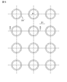
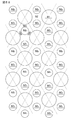
- the central portion (top) of the first light reflecting layer of each light emitting element is not limited, but may be formed so as to be located on the apex (intersection) of the square lattice. It can, or it can be in the form of being located on the apex (intersection) of an equilateral triangle grid.
- the laminated structure is at least one kind of material selected from the group consisting of a GaN-based compound semiconductor, an InP-based compound semiconductor, and a GaAs-based compound semiconductor. It can be composed of.
- the laminated structure (A) Structure made of GaN-based compound semiconductor (b) Structure made of InP-based compound semiconductor (c) Structure made of GaAs-based compound semiconductor (d) Structure made of GaN-based compound semiconductor and InP-based compound semiconductor (e) GaN-based Configuration of compound semiconductors and GaAs-based compound semiconductors (f) Configuration of InP-based compound semiconductors and GaAs-based compound semiconductors (g) Configuration of GaN-based compound semiconductors, InP-based compound semiconductors, and GaAs-based compound semiconductors. ..
- the laminated structure can be more specifically composed of, for example, an AlInGaN-based compound semiconductor.
- AlInGaN-based compound semiconductor more specifically, GaN, AlGaN, InGaN, and AlInGaN can be mentioned.
- these compound semiconductors may contain a boron (B) atom, a thallium (Tl) atom, an arsenic (As) atom, a phosphorus (P) atom, and an antimony (Sb) atom, if desired. ..
- the active layer preferably has a quantum well structure.
- the active layer having a quantum well structure has a structure in which at least one well layer and a barrier layer are laminated, but as a combination of (compound semiconductors constituting the well layer and compound semiconductors constituting the barrier layer), ( In y Ga (1-y) N, GaN), (In y Ga (1-y) N, In z Ga (1-z) N) [However, y> z], (In y Ga (1-y) ) N, AlGaN) can be exemplified.
- the first compound semiconductor layer is composed of a first conductive type (for example, n type) compound semiconductor
- the second compound semiconductor layer is made of a second conductive type (for example, p type) compound semiconductor different from the first conductive type.
- the first compound semiconductor layer and the second compound semiconductor layer are also referred to as a first clad layer and a second clad layer.
- the first compound semiconductor layer and the second compound semiconductor layer may be a layer having a single structure, a layer having a multilayer structure, or a layer having a superlattice structure. Further, it may be a layer provided with a composition gradient layer and a concentration gradient layer.
- gallium (Ga), indium (In), and aluminum (Al) can be mentioned as group III atoms constituting the laminated structure
- arsenic (As) can be mentioned as the group V atoms constituting the laminated structure.
- GaNAs, GaInNAs, and examples of the compound semiconductor constituting the active layer include GaAs, AlGaAs, GaInAs, GaInAsP, GaInP, GaSb, GaAsSb, GaN, InN, GaInN, GaInNAs, and GaInNAsSb.
- the quantum well structure examples include a two-dimensional quantum well structure, a one-dimensional quantum well structure (quantum wire), and a zero-dimensional quantum well structure (quantum dot).
- Materials constituting the quantum well include, for example, Si; Se; calcopyrite compounds CIGS (CuInGaSe), CIS (CuInSe 2 ), CuInS 2 , CuAlS 2 , CuAlSe 2 , CuGaS 2 , CuGaSe 2 , AgAlS 2 , AgAlSe.
- Perovskite-based material Perovskite-based material; Group III-V compounds GaAs, GaP, InP, AlGaAs, InGaP, AlGaInP, InGaAsP, GaN, InAs, InGaAs, GaInNAs, GaSb, GaAsSb; CdSe, CdSe, Cd , CdTe, In 2 Se 3 , In 2 S 3 , Bi 2 Se 3 , Bi 2 S 3 , ZnSe, ZnTe, ZnS, HgTe, HgS, PbSe, PbS, TiO 2, etc., but are limited to these. It is not something to do.
- the GaAs and InP materials also have a sphalerite structure.
- the main surface of the compound semiconductor substrate composed of these materials include surfaces turned off in a specific direction in addition to surfaces such as (100), (111) AB, (211) AB, and (311) AB. it can.
- "AB” means that the 90 ° off direction is different, and whether the main material of the surface is group III or group V is determined by this off direction.
- the film forming method the MBE method, the MOCVD method, the MEE method, the ALD method and the like are generally used as in the GaN system, but the film forming method is not limited to these methods.
- trimethylgallium (TMG) gas and triethylgallium (TEG) gas can be mentioned as the organic gallium source gas in the MOCVD method, and ammonia gas and hydrazine as the nitrogen source gas. Gas can be mentioned.
- silicon (Si) may be added as an n-type impurity (n-type dopant)
- the GaN-based compound semiconductor having a p-type conductive type may be added.
- magnesium (Mg) may be added as a p-type impurity (p-type dopant).
- trimethylaluminum (TMA) gas may be used as the Al source, or trimethylindium (TMI) gas may be used as the In source.
- TMA trimethylaluminum
- TMI trimethylindium
- monosilane gas (SiH 4 gas) may be used as the Si source
- biscyclopentadienyl magnesium gas, methylcyclopentadienyl magnesium, or biscyclopentadienyl magnesium (Cp 2 Mg) may be used as the Mg source. Good.
- n-type impurities n-type dopants
- p-type impurities p-type dopants
- Mg, Zn, Cd, Be, Ca, Ba, C, Hg, and Sr can be mentioned.
- organometallic raw materials such as TMGa, TEGa, TMIn, and TMAl are generally used as the group III raw materials.
- group V raw material arsine gas (AsH 3 gas), phosphine gas (PH 3 gas), ammonia (NH 3 ) and the like are used.
- group V raw material an organic metal raw material may be used, and examples thereof include tertiary butylarsine (TBAs), tertiary butylphosphine (TBP), dimethylhydrazine (DMHy), and trimethylantimony (TMSb). Can be done.
- n-type dopant monosilane (SiH 4 ) is used as the Si source, hydrogen selenide (H 2 Se) or the like is used as the Se source.
- p-type dopant dimethylzinc (DMZn), biscyclopentadienyl magnesium (Cp 2 Mg) and the like are used.
- DMZn dimethylzinc
- Cp 2 Mg biscyclopentadienyl magnesium
- the laminated structure is formed on the second surface of the light emitting device manufacturing substrate, or is also formed on the second surface of the compound semiconductor substrate.
- the second surface of the light emitting device manufacturing substrate or the compound semiconductor substrate faces the first surface of the first compound semiconductor layer, and the first surface of the light emitting element manufacturing substrate or the compound semiconductor substrate is the light emitting element manufacturing substrate. Facing the second surface of.
- GaN substrate As substrates for manufacturing light emitting elements, GaN substrate, sapphire substrate, GaAs substrate, SiC substrate, alumina substrate, ZnS substrate, ZnO substrate, AlN substrate, LiMgo substrate, LiGaO 2 substrate, MgAl 2 O 4 substrate, InP substrate, Si substrate, Examples thereof include those having a base layer and a buffer layer formed on the surface (main surface) of these substrates, but the use of a GaN substrate is preferable because the defect density is low. Further, examples of the compound semiconductor substrate include a GaN substrate, an InP substrate, and a GaAs substrate.
- any main surface (second surface) of the GaN substrate can be used for forming a compound semiconductor layer. ..
- the main surface of the GaN substrate depending on the crystal structure (for example, cubic type, hexagonal type, etc.), names such as so-called A-plane, B-plane, C-plane, R-plane, M-plane, N-plane, S-plane, etc. It is also possible to use the crystal plane orientation referred to in (1), or a plane in which these are turned off in a specific direction.
- an organic metal chemical vapor deposition method MOCVD method, Metal Organic-Chemical Vapor Deposition method, MOVPE method, Metal Organic-Vapor Phase Epitaxy method
- MOCVD method Metal Organic-Chemical Vapor Deposition method
- MOVPE method Metal Organic-Vapor Phase Epitaxy method
- MBE method molecule Molecular beam epitaxy method
- HVPE method hydride vapor phase growth method in which halogen contributes to transport or reaction
- ALD method Atomic Layer Deposition method
- MEE method migration enhanced epitaxy method
- MEE method MEE method
- Migration-Enhanced Epitaxy method plasma assisted physical vapor deposition method
- PPD method plasma assisted physical vapor deposition method
- the substrate for manufacturing the light emitting device may be left as it is, or the active layer, the second compound semiconductor layer, the second electrode, and the second light reflecting layer may be left on the first compound semiconductor layer. May be sequentially formed, and then the light emitting element manufacturing substrate may be removed. Specifically, an active layer, a second compound semiconductor layer, a second electrode, and a second light-reflecting layer were sequentially formed on the first compound semiconductor layer, and then the second light-reflecting layer was fixed to a support substrate. After that, the substrate for manufacturing the light emitting element may be removed to expose the first compound semiconductor layer (the first surface of the first compound semiconductor layer).
- an alkaline aqueous solution such as a sodium hydroxide aqueous solution or a potassium hydroxide aqueous solution, an ammonia solution + hydrogen peroxide solution, a sulfuric acid solution + hydrogen peroxide solution, a hydrochloric acid solution + hydrogen peroxide solution, or a phosphoric acid solution.
- + Wet etching method using aqueous hydrogen solution chemical mechanical polishing method (CMP method), mechanical polishing method, dry etching method such as reactive ion etching (RIE) method, lift-off method using laser, etc.
- the support substrate may be composed of, for example, various substrates exemplified as a substrate for manufacturing a light emitting element, or an insulating substrate made of AlN or the like, a semiconductor substrate made of Si, SiC, Ge or the like, a metal substrate, or the like.
- a conductive substrate or a metal substrate or an alloy substrate can be used from the viewpoints of mechanical properties, elastic deformation, plastic deformability, heat dissipation, and the like. It is preferable to use it.
- As the thickness of the support substrate for example, 0.05 mm to 1 mm can be exemplified.
- solder bonding method As a method for fixing the second light reflecting layer to the support substrate, known methods such as a solder bonding method, a room temperature bonding method, a bonding method using an adhesive tape, a bonding method using a wax bonding, and a method using an adhesive are used. Although it can be used, it is desirable to adopt a solder bonding method or a room temperature bonding method from the viewpoint of ensuring conductivity.
- a silicon semiconductor substrate which is a conductive substrate
- the bonding temperature may be 400 ° C. or higher.
- the first electrode electrically connected to the first compound semiconductor layer is common to a plurality of light emitting elements
- the second electrode electrically connected to the second compound semiconductor layer is common to a plurality of light emitting elements. Yes, or it can be in the form of being individually provided in a plurality of light emitting elements.
- the first electrode may be formed on the first surface facing the second surface of the light emitting element manufacturing substrate, or may be formed on the second surface of the compound semiconductor substrate. It may be formed on the first surface facing the above surface.
- the light emitting element manufacturing substrate is not left, it may be formed on the first surface of the first compound semiconductor layer constituting the laminated structure.
- the first electrode since the first light reflecting layer is formed on the first surface of the first compound semiconductor layer, for example, the first electrode may be formed so as to surround the first light reflecting layer.
- the first electrode is, for example, gold (Au), silver (Ag), palladium (Pd), platinum (Pt), nickel (Ni), Ti (titanium), vanadium (V), tungsten (W), chromium (Cr). ), Al (aluminum), Cu (copper), Zn (zinc), tin (Sn) and indium (In), including at least one metal (including alloy) selected from the group. It is desirable to have a multi-layer structure, specifically, for example, Ti / Au, Ti / Al, Ti / Al / Au, Ti / Pt / Au, Ni / Au, Ni / Au / Pt, Ni / Pt, Pd.
- the first electrode can be formed by a PVD method such as a vacuum vapor deposition method or a sputtering method.
- the first electrode When the first electrode is formed so as to surround the first light reflecting layer, the first light reflecting layer and the first electrode can be in contact with each other. Alternatively, the first light reflecting layer and the first electrode can be separated from each other. In some cases, a state in which the first electrode is formed on the edge of the first light reflecting layer and a state in which the first light reflecting layer is formed on the edge of the first electrode are mentioned. You can also.
- planar shape of the first light reflecting layer, the protruding portion, and the second light reflecting layer examples include a circle, an ellipse, an oval, a rectangle, and a regular polygon (regular triangle, square, regular hexagon, etc.). Can be done. Further, it is desirable that the first light reflecting layer, the protruding portion, and the second light reflecting layer have a similar shape or an approximate shape.
- the second electrode can be made of a transparent conductive material.
- an indium-based transparent conductive material specifically, for example, indium-tin oxide (ITO, Indium Tin Oxide, Sn-doped In 2 O 3 , crystalline ITO and Including amorphous ITO), indium-zinc oxide (IZO, Indium Zinc Oxide), indium-gallium oxide (IGO), indium-doped gallium-zinc oxide (IGZO, In-GaZnO 4 ), IFO (F-doped) in 2 O 3) of, ITiO (Ti-doped in 2 O 3), InSn, InSnZnO], the tin-based transparent conductive material [specifically, for example, tin oxide (SnO X), SnO of ATO (Sb-doped 2 ), FTO (F-doped SnO 2 )], zinc-based transparent conductive material [specifically, for example, zinc
- Dope zinc oxide (GZO), AlMgZnO (aluminum oxide and magnesium oxide-doped zinc oxide)], NiO, TiO X , graphene can be exemplified.
- a transparent conductive film having a gallium oxide, titanium oxide, niobium oxide, antimony oxide, nickel oxide or the like as a base layer can be mentioned, and a spinel-type oxide, YbFe 2
- a transparent conductive material such as an oxide having an O 4 structure can also be mentioned.
- the material constituting the second electrode depends on the arrangement state of the second light reflecting layer and the second electrode, but is not limited to the transparent conductive material, and palladium (Pd), platinum (Pt), and the like.
- the second electrode may be composed of at least one of these materials.
- the second electrode can be formed by a PVD method such as a vacuum vapor deposition method or a sputtering method.
- a low-resistance semiconductor layer can be used as the transparent electrode layer, and in this case, specifically, an n-type GaN-based compound semiconductor layer can also be used.
- the electrical resistance at the interface can be reduced by joining the two via a tunnel junction.
- a first pad electrode and a second pad electrode are provided on the first electrode and the second electrode in order to electrically connect to an external electrode or circuit (hereinafter, may be referred to as "external circuit or the like"). You may.
- the pad electrode is a single layer containing at least one metal selected from the group consisting of Ti (titanium), aluminum (Al), Pt (platinum), Au (gold), Ni (nickel), Pd (palladium). It is desirable to have a configuration or a multi-layer configuration.
- the pad electrode has a Ti / Pt / Au multi-layer structure, a Ti / Au multi-layer structure, a Ti / Pd / Au multi-layer structure, a Ti / Pd / Au multi-layer structure, and a Ti / Ni / Au multi-layer structure.
- the multilayer configuration exemplified by the multilayer configuration of Ti / Ni / Au / Cr / Au can also be used.
- a cover metal layer made of, for example, Ni / TiW / Pd / TiW / Ni is formed on the surface of the first electrode, and a cover metal layer is formed on the cover metal layer.
- the light reflecting layer (distributed Bragg reflector layer, distributed Bragg Reflector layer, DBR layer) constituting the first light reflecting layer and the second light reflecting layer is composed of, for example, a semiconductor multilayer film or a dielectric multilayer film.
- the dielectric material for example, Si, Mg, Al, Hf , Nb, Zr, Sc, Ta, Ga, Zn, Y, B, oxides such as Ti, nitrides (e.g., SiN X, AlN X, AlGaN X , GaN X , BN X, etc.), or fluoride and the like.
- the light reflecting layer can be obtained by alternately laminating two or more kinds of dielectric films made of dielectric materials having different refractive indexes among these dielectric materials.
- each dielectric film may be appropriately selected.
- the thickness of each dielectric film, a material or the like to be used, as appropriate, can be adjusted, the oscillation wavelength (emission wavelength) lambda 0, is determined by the refractive index n of the oscillation wavelength lambda 0 of the material used. Specifically, it is preferably an odd multiple of ⁇ 0 / (4n).
- the light-emitting element of the oscillation wavelength lambda 0 is 410 nm
- when forming the light reflecting layer from SiO X / NbO Y it may be exemplified about 40nm to 70 nm.
- the number of layers can be exemplified by 2 or more, preferably about 5 to 20.
- As the thickness of the entire light reflecting layer for example, about 0.6 ⁇ m to 1.7 ⁇ m can be exemplified. Further, it is desirable that the light reflectance of the light reflecting layer is 95% or more.
- the size and shape of the light reflecting layer are not particularly limited as long as they cover the current injection region or the element region (which will be described later).
- the light reflecting layer can be formed based on a well-known method, and specifically, for example, a vacuum vapor deposition method, a sputtering method, a reactive sputtering method, an ECR plasma sputtering method, a magnetron sputtering method, an ion beam assisted vapor deposition method, and the like.
- PVD method such as ion plating method, laser ablation method; various CVD methods; coating method such as spray method, spin coating method, dip method; method of combining two or more of these methods; these methods and whole or partial Pretreatment, irradiation of inert gas (Ar, He, Xe, etc.) or plasma, irradiation of oxygen gas, ozone gas, plasma, oxidation treatment (heat treatment), exposure treatment, etc. Can be mentioned.
- inert gas Ar, He, Xe, etc.
- plasma irradiation of oxygen gas, ozone gas, plasma, oxidation treatment (heat treatment), exposure treatment, etc.
- a current injection area is provided to regulate the current injection into the active layer.
- the shape of the boundary between the current injection region and the current non-injection / inner region, the shape of the boundary between the current non-injection / inner region and the current non-injection / outer region, and the planar shape of the opening provided in the element region or the current constriction region Specific examples thereof include circles, ellipses, oval, rectangles, and regular polygons (regular triangles, squares, regular hexagons, etc.). It is desirable that the shape of the boundary between the current injection region and the current non-injection / inner region and the shape of the boundary between the current non-injection / inner region and the current non-injection / outer region are similar figures or approximate shapes.
- the "element region” is a region in which a narrowed current is injected, a region in which light is confined due to a difference in refractive index, or is sandwiched between a first light reflecting layer and a second light reflecting layer. It refers to a region in which laser oscillation occurs, or a region sandwiched between the first light reflecting layer and the second light reflecting layer, which actually contributes to laser oscillation.
- bumps may be arranged on the second surface of the light emitting element (exposed surface of the light emitting element on the second light reflecting layer side).
- the bumps include gold (Au) bumps, solder bumps, and indium (In) bumps, and the method of arranging the bumps can be a well-known method.
- the bump is provided on the second pad electrode provided on the second electrode, or is also provided on the extending portion of the second pad electrode.
- a brazing material can be used instead of the bump.
- brazing material for example, In (indium: melting point 157 ° C); indium-gold-based low melting point alloy; Sn 80 Ag 20 (melting point 220 to 370 ° C), Sn 95 Cu 5 (melting point 227 to 370 ° C).
- Tin (Sn) -based high-temperature solder such as Pb 97.5 Ag 2.5 (melting point 304 ° C), Pb 94.5 Ag 5.5 (melting point 304-365 ° C), Pb 97.5 Ag 1.5 Sn 1.0 (melting point 309 ° C) and other lead (melting point 309 ° C) Pb) -based high-temperature solder; tin (Zn) -based high-temperature solder such as Zn 95 Al 5 (melting point 380 ° C); Sn 5 Pb 95 (melting point 300 to 314 ° C), Sn 2 Pb 98 (melting point 316 to 322 ° C) ) Etc. tin-lead standard solder; brazing materials such as Au 88 Ga 12 (melting point 381 ° C) (all the above subscripts represent atomic%) can be exemplified.
- the side surface or the exposed surface of the laminated structure may be covered with a coating layer (insulating film).
- the coating layer (insulating film) can be formed based on a well-known method.
- the refractive index of the material constituting the coating layer (insulating film) is preferably smaller than the refractive index of the material constituting the laminated structure.
- the material constituting the coating layer (insulating film) illustrated SiO X based material containing SiO 2, SiN X-based material, SiO Y N Z material, TaO X, ZrO X, AlN X, AlO X, a GaO X
- an organic material such as a polyimide resin can be mentioned.
- a method for forming the coating layer (insulating film) for example, a PVD method such as a vacuum deposition method or a sputtering method, a CVD method, or a coating method can be used for forming the coating layer (insulating film).
- Example 1 relates to a light emitting element according to the first aspect of the present disclosure, a method for manufacturing a light emitting element according to the first aspect of the present disclosure, and a light emitting element array of the present disclosure.
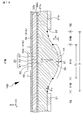
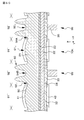
- a schematic partial cross-sectional view of the light emitting element of Example 1 is shown in FIG. 1, and a schematic partial cross-sectional view of a light emitting element array having a plurality of light emitting elements of Example 1 is shown in FIG.
- FIG. 3 and FIG. 4 show schematic partial cross-sectional views of Modification 1 and Modification 2 of the light emitting element of Example 1, and the first light reflection in the light emitting element array composed of a plurality of the light emitting elements of Example 1.
- FIGS. 5 and 6 Schematic plan views of the arrangement of the layers and the first electrode are shown in FIGS. 5 and 6.
- a schematic partial cross-sectional view of the light emitting element or the light emitting element array is a schematic partial cross-sectional view taken along the arrows AA of FIGS. 5 and 6, and FIG. 5 shows a square light emitting element.
- FIG. 5 shows a square light emitting element.
- FIG. 6 shows the case where the light emitting element is located on the apex (intersection) of the equilateral triangle lattice.
- the Z axis indicates the axis of the first light reflecting layer 41 (a perpendicular line passing through the center of the first light reflecting layer 41 and with respect to the laminated structure 20) constituting the light emitting element.
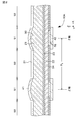
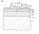
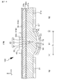
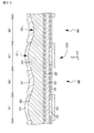
- the light emitting elements of Example 1 or Examples 2 to 24 described later are A first compound semiconductor layer 21 having a first surface 21a and a second surface 21b facing the first surface 21a, The active layer (light emitting layer) 23 facing the second surface 21b of the first compound semiconductor layer 21, and A second compound semiconductor layer 22 having a first surface 22a facing the active layer 23 and a second surface 22b facing the first surface 22a, Laminated structure 20, The first light reflecting layer 41, and The second light reflecting layer 42, which is formed on the second surface side of the second compound semiconductor layer 22 and has a flat shape, Is equipped with The base surface 90 located on the first surface side of the first compound semiconductor layer 21 includes a protruding portion 91 projecting in a direction away from the active layer 23.
- the cross-sectional shape of the protruding portion 91 when the base surface 90 is cut in a virtual plane (for example, an XZ plane in the illustrated example) including the stacking direction of the laminated structure 20 is composed of a smooth curve.
- the first light reflecting layer 41 is formed on at least the protruding portion 91.
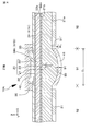
- the diameter of the protruding portion 91 is D 1
- the height of the protruding portion 91 is H 1
- the radius of curvature of the top of the protruding portion 91 is R 1
- the surface of the protruding portion 91 is D 1
- the light emitting element array of the first embodiment is It is composed of multiple light emitting elements. Each light emitting element is composed of the light emitting element 10A of the first embodiment.
- the formation pitch P 0 of the light emitting element (distance from the axis of the first light reflecting layer 41 constituting the light emitting element to the axis of the first light reflecting layer 41 constituting the adjacent light emitting element) is 3 ⁇ 10 -5 m.
- the first surface 21a of the first compound semiconductor layer 21 constitutes the base surface 90. That is, the light emitting element 10A of the first embodiment is a light emitting element having the first configuration.
- the first light reflecting layer 41 is formed at least on the protruding portion 91, but specifically, the first light reflecting layer 41 is formed on the protruding portion 91.
- the present invention is not limited to this, and the extending portion of the first light reflecting layer 41 may be formed in a region other than the protruding portion 91 of the base surface 90.
- a region other than the region where the protruding portion 91 of the base surface 90 is formed is indicated by reference numeral 92, and is hereinafter referred to as a “second region” for convenience.
- the protrusion 91 when the protrusion 91 is cut in a virtual plane (for example, an XZ plane in the illustrated example) including the stacking direction (Z-axis direction) of the laminated structure 20.
- the figure drawn by the protrusion 91 is, for example, a part of a circle.
- the laminated structure 20 can be composed of at least one material selected from the group consisting of a GaN-based compound semiconductor, an InP-based compound semiconductor, and a GaAs-based compound semiconductor. Specifically, in the first embodiment, the laminated structure 20 is made of a GaN-based compound semiconductor.
- the first compound semiconductor layer 21 is composed of, for example, an n-GaN layer doped with Si about 2 ⁇ 10 16 cm -3
- the active layer 23 is an In 0.04 Ga 0.96 N layer (barrier layer). It is composed of a five-layered multiple quantum well structure in which In 0.16 Ga 0.84 N layers (well layers) are laminated
- the second compound semiconductor layer 22 is, for example, p-, which is doped with magnesium by about 1 ⁇ 10 19 cm -3. It consists of a GaN layer.
- the plane orientation of the first compound semiconductor layer 21 is not limited to the ⁇ 0001 ⁇ plane, and may be, for example, a ⁇ 20-21 ⁇ plane which is a semi-polar plane.
- the first electrode 31 made of Ti / Pt / Au is electrically connected to an external circuit or the like via, for example, a first pad electrode (not shown) made of Ti / Pt / Au or V / Pt / Au.
- the second electrode 32 is formed on the second compound semiconductor layer 22, and the second light reflecting layer 42 is formed on the second electrode 32.
- the second light reflecting layer 42 on the second electrode 32 has a flat shape.
- the second electrode 32 is made of a transparent conductive material, specifically, ITO having a thickness of 30 nm.
- the pad electrode 33 may be formed or connected (see FIGS. 3 and 4).
- the first light reflecting layer 41 and the second light reflecting layer 42 have a laminated structure of a Ta 2 O 5 layer and a SiO 2 layer, or a laminated structure of a SiN layer and a SiO 2 layer. Although the first light reflecting layer 41 and the second light reflecting layer 42 have a multilayer structure in this way, they are represented by one layer for the sake of simplification of drawings.
- first electrode 31 specifically, the opening 31'provided in the first electrode 31
- first light reflecting layer 41 the first light reflecting layer 41
- second light reflecting layer 42 the insulating layer (current constriction layer) 34.
- planar shape of each of the openings 34A is circular.
- the insulating material between the second electrode 32 and the second compound semiconductor layer 22 e.g., SiO X and SiN X, AlO X
- the insulating layer (current constriction layer) 34 is provided with an opening 34A for injecting a current into the second compound semiconductor layer 22.
- the second compound semiconductor layer 22 may be etched by the RIE method or the like to form a mesa structure.
- a part of the laminated second compound semiconductor layer 22 may be partially oxidized from the lateral direction to form a current constriction region.
- an impurity for example, boron
- an impurity for example, boron
- these may be combined as appropriate.
- the second electrode 32 needs to be electrically connected to the portion (current injection region) of the second compound semiconductor layer 22 through which a current flows due to current constriction.
- the second electrode 32 is common to the light emitting elements 10A constituting the light emitting element array, and the second electrode 32 is connected to an external circuit or the like via the first pad electrode (not shown). Be connected.
- the first electrode 31 is also common to the light emitting elements 10A constituting the light emitting element array, and is connected to an external circuit or the like via the first pad electrode (not shown). Then, the light may be emitted to the outside through the first light reflecting layer 41, or the light may be emitted to the outside through the second light reflecting layer 42.
- the second electrode 32 is individually formed in the light emitting element 10A constituting the light emitting element array. It is connected to an external circuit or the like via the second pad electrode 33.
- the first electrode 31 is common to the light emitting elements 10A constituting the light emitting element array, and is connected to an external circuit or the like via the first pad electrode (not shown). Then, the light may be emitted to the outside through the first light reflecting layer 41, or the light may be emitted to the outside through the second light reflecting layer 42.
- FIG. 4 a schematic partial cross-sectional view of a modification 2 of the light emitting element 10A of the first embodiment
- the second electrode 32 is individually formed in the light emitting element 10A constituting the light emitting element array.
- a bump 35 is formed on the second pad electrode 33 formed on the second electrode 32, and is connected to an external circuit or the like via the bump 35.
- the first electrode 31 is common to the light emitting elements 10A constituting the light emitting element array, and is connected to an external circuit or the like via the first pad electrode (not shown).
- the bumps 35 are arranged on the second surface side portion of the second compound semiconductor layer 22 facing the base surface 90, and cover the second light reflecting layer 42.
- Examples of the bump 35 include a gold (Au) bump, a solder bump, and an indium (In) bump.
- the method of arranging the bumps 35 can be a well-known method. Then, the light is emitted to the outside through the first light reflecting layer 41.
- the bump 35 may be provided in the light emitting element 10A shown in FIG. Examples of the shape of the bump 35 include a cylindrical shape, an annular shape, and a hemispherical shape.
- the value of the thermal conductivity of the laminated structure 20 is higher than the value of the thermal conductivity of the first light reflecting layer 41.
- the value of the thermal conductivity of the dielectric material constituting the first light reflecting layer 41 is about 10 watts / (m ⁇ K) or less.
- the value of the thermal conductivity of the GaN-based compound semiconductor constituting the laminated structure 20 is about 50 watts / (m ⁇ K) to about 100 watts / (m ⁇ K).
- FIGS. 7A, 7B, 8, 8, 9, 10A, 10B, and 10C are schematic partial end views of the first compound semiconductor layer and the like.
- the manufacturing method will be described, but the manufacturing method of the light emitting element of the first embodiment or the second embodiment described later is described.
- the base surface 90 located on the first surface side of the first compound semiconductor layer 21 includes a protruding portion 91 projecting in a direction away from the active layer 23.
- the cross-sectional shape of the protruding portion 91 when the base surface 90 is cut in a virtual plane (XZ plane) including the stacking direction of the laminated structure 20 is a method for manufacturing a light emitting element having a smooth curve.
- the second light reflecting layer 42 is formed on the second surface side of the second compound semiconductor layer 22, and then the second light reflecting layer 42 is formed.
- a first sacrificial layer 81 is formed on the base surface 90 on which the protrusion 91 should be formed, and then the first sacrificial layer 81 is formed.
- a second sacrificial layer 82 is formed on the entire surface, and then the second sacrificial layer 82 and the first sacrificial layer 81 are used as an etching mask and etched back from the base surface 90 toward the inside thereof to form the base surface 90.
- a protrusion 91 is formed, and then the protrusion 91 is formed.
- a first light reflecting layer 41 is formed on at least the protrusion 91. Each process is provided.
- Step-100 Specifically, on the second surface 11b of the compound semiconductor substrate 11 having a thickness of about 0.4 mm, A first compound semiconductor layer 21 having a first surface 21a and a second surface 21b facing the first surface 21a, The active layer (light emitting layer) 23 facing the second surface 21b of the first compound semiconductor layer 21, and A second compound semiconductor layer 22 having a first surface 22a facing the active layer 23 and a second surface 22b facing the first surface 22a, A laminated structure 20 made of a GaN-based compound semiconductor is formed. More specifically, the first compound semiconductor layer 21, the active layer 23, and the second compound semiconductor layer 22 are sequentially formed on the second surface 11b of the compound semiconductor substrate 11 based on the well-known epitaxial growth method by the MOCVD method. By doing so, the laminated structure 20 can be obtained (see FIG. 7A).
- an opening 34A is provided on the second surface 22b of the second compound semiconductor layer 22 based on a combination of a film forming method such as a CVD method, a sputtering method, or a vacuum vapor deposition method and a wet etching method or a dry etching method.
- An insulating layer (current constriction layer) 34 made of SiO 2 is formed (see FIG. 7B).
- the insulating layer 34 having the opening 34A defines a current constriction region (current injection region 61A and current non-injection region 61B). That is, the opening 34A defines the current injection region 61A.
- an insulating material between the second electrode 32 and the second compound semiconductor layer 22 e.g., SiO X and SiN X, AlO X
- the insulating layer (current constriction layer) 34 may be provided with an opening 34A for injecting a current into the second compound semiconductor layer 22.
- the second compound semiconductor layer 22 may be etched by the RIE method or the like to form a mesa structure.
- a part of the laminated second compound semiconductor layer 22 may be partially oxidized from the lateral direction to form a current constriction region.
- an impurity for example, boron
- an impurity for example, boron
- these may be combined as appropriate.
- the second electrode 32 needs to be electrically connected to the portion (current injection region) of the second compound semiconductor layer 22 through which a current flows due to current constriction.
- the second electrode 32 and the second light reflecting layer 42 are formed on the second compound semiconductor layer 22.
- the second electrode 32 is mounted on the insulating layer 34 from the second surface 22b of the second compound semiconductor layer 22 exposed on the bottom surface of the opening 34A (current injection region 61A), for example, based on the lift-off method.
- the second pad electrode 33 is formed based on a combination of a film forming method such as a sputtering method or a vacuum vapor deposition method and a patterning method such as a wet etching method or a dry etching method, if desired.
- the second light reflecting layer is laid over the second electrode 32 and over the second pad electrode 33, based on a combination of a film forming method such as a sputtering method or a vacuum vapor deposition method and a patterning method such as a wet etching method or a dry etching method.
- a film forming method such as a sputtering method or a vacuum vapor deposition method
- a patterning method such as a wet etching method or a dry etching method.
- the second light reflecting layer 42 is fixed to the support substrate 49 via the bonding layer 48 (see FIG. 9). Specifically, the second light reflecting layer 42 (or bump 35) is fixed to the support substrate 49 composed of the sapphire substrate by using the bonding layer 48 made of an adhesive.
- the compound semiconductor substrate 11 is thinned based on a mechanical polishing method or a CMP method, and further etched to remove the compound semiconductor substrate 11.
- the first sacrificial layer 81 is formed on the base surface 90 on which the protrusion 91 should be formed. Specifically, on the region where the protruding portion 91 of the base surface 90 (more specifically, the first surface 21a of the first compound semiconductor layer 21) on which the first light reflecting layer 41 is to be formed is to be formed, The first sacrificial layer 81 (specifically, the first sacrificial layer 81 having a rectangular cross-sectional shape in the XZ plane) is formed. More specifically, the first resist material layer is formed on the first surface 21a of the first compound semiconductor layer 21, and the first resist material layer is left on the region where the protrusion 91 should be formed.
- the first sacrificial layer 81 shown in FIG. 10A is obtained. It is not necessary to heat the first sacrificial layer 81 to deform its cross-sectional shape. In this way, the first sacrificial layer 81 can be formed on the base surface 90 on which the protrusion 91 should be formed. In some cases, when the surface of the first sacrificial layer 81 is subjected to an ashing treatment (plasma irradiation treatment), the surface of the first sacrificial layer 81 is altered, and the second sacrificial layer 82 is formed in the next step, the first sacrificial layer 82 is formed.
- an ashing treatment plasma irradiation treatment
- the first resist material layer may be heated or irradiated with ultraviolet rays for curing the first resist material layer.
- a second sacrificial layer 82 is formed on the entire surface (see FIG. 10B), and then the second sacrificial layer 82 and the first sacrificial layer 81 are used as an etching mask from the base surface 90 to the inside thereof (that is, the first compound).
- a protruding portion 91 is formed on the base surface 90 (see FIG. 10C).
- the connecting portion between the protruding portion 91 and the second region 92 is indicated by a black square.
- Etching back can be performed based on a dry etching method such as the RIE method, or can be performed based on a wet etching method using hydrochloric acid, nitric acid, hydrofluoric acid, phosphoric acid, a mixture thereof, or the like. If the second sacrificial layer 82 is formed so that the value of the surface roughness Rq of the second sacrificial layer 82 is smaller than the value of the surface roughness Rq of the first compound semiconductor layer 21, the protruding portion 91 after etching back can be formed. The value of the surface roughness Rq can be made smaller than that before the etch back, the scattering loss can be suppressed, and the performance as a resonator can be improved.
- the value of the surface roughness Rq of the second sacrificial layer 82 is preferably 0.3 nm or less. Further, it is preferable that the etching rates of the second sacrificial layer 82, the first sacrificial layer 81, and the base surface 90 are the same.
- the surface roughness Rq is specified in JIS B-610: 2001, and can be specifically measured based on observation based on AFM or cross-sectional TEM.
- a second sacrificial layer 82 made of, for example, a photoresist is formed on the entire surface based on the spin coating method.
- the film thickness of the second sacrificial layer 82 needs to be thinner than the film thickness at which the surface of the second sacrificial layer 82 including the top of the first sacrificial layer 81 becomes flat.
- the rotation speed in the spin coating method is 10 rpm or more, and for example, 6000 rpm is preferable.
- the second sacrificial layer 82 accumulates at the boundary between the first sacrificial layer 81 and the first compound semiconductor layer 21.
- the second sacrificial layer 82 is subjected to baking treatment.
- the baking temperature is 90 ° C.
- the second sacrificial layer 82 in which the shape above the first sacrificial layer 81 is convex and the upper part of the hem of the first sacrificial layer 81 is divergent. Then, based on the RIE method using SiC 4 gas and Cl 2 gas as etching gases, the second sacrificial layer 82 and the first sacrificial layer 81 are used as etching masks from the base surface 90 to the inside (that is, the first compound). By etching back from the first surface 21a of the semiconductor layer 21 toward the inside of the first compound semiconductor layer 21), the protruding portion 91 can be formed on the base surface 90.
- the second sacrificial layer 82 when the second sacrificial layer 82 is formed on the entire surface, the second sacrificial layer 82 may be formed a plurality of times.
- the second sacrificial layer 82 after forming the protrusion 91 on the base surface 90, the second sacrificial layer 82 is formed on the entire surface, and then the second sacrificial layer 82 is used as an etching mask from the base surface 90 to the inside (that is, the first).
- a protruding portion 91 may be formed on the base surface 90 by etching back from the first surface 21a of the one-compound semiconductor layer 21 toward the inside of the first compound semiconductor layer 21).
- the second sacrificial layer 82 may be formed a plurality of times.
- the first sacrificial layer 81 may be formed based on the nanoimprint method in [Step-150].
- the first sacrificial layer 81 is used as an etching mask from the base surface 90 to the inside thereof (that is, from the first surface 21a to the first compound semiconductor of the first compound semiconductor layer 21).
- the second sacrificial layer 82 is formed on the entire surface, and then the second sacrificial layer 82 is used as an etching mask from the base surface 90 to the inside thereof.
- the protruding portion 91 can be formed on the base surface 90 by etching back toward (that is, from the first surface 21a of the first compound semiconductor layer 21 to the inside of the first compound semiconductor layer 21).
- the materials constituting the first sacrificial layer 81 and the second sacrificial layer 82 are not limited to the resist material, but are limited to ceramic materials such as SOG, oxide materials (for example, SiO 2 , SiN, TiO 2, etc.), and semiconductor materials (for example, An appropriate material for the first compound semiconductor layer 21, such as Si, GaN, InP, GaAs, etc.), a metal material (for example, Ni, Au, Pt, Sn, Ga, In, Al, etc.) may be selected.
- the thickness of the first sacrificial layer 81 and the thickness of the second sacrificial layer 82 can be obtained.
- appropriately set the diameter or the like of the first sacrificial layer 81 by selecting, of the convex radius of curvature R 1 values and base surface 90 of the projecting portion 91 shaped (e.g., diameter D 1 and a height H 1), The cross-sectional shape of the protruding portion 91 can be a desired value and shape. The same applies to Examples 2 to 3 described later.
- FIG. 11 shows a graph showing the relationship between the resist material constituting the second sacrificial layer 82, the diameter D 1 of the protruding portion 91, and the radius of curvature R 1 of the top of the protruding portion 91.
- the first light reflecting layer 41 is formed on the top of at least the protruding portion 91 of the base surface 90. Specifically, the first light reflecting layer 41 is formed on the entire surface of the base surface 90 based on a film forming method such as a sputtering method or a vacuum vapor deposition method, and then the first light reflecting layer 41 is patterned to form a base surface. The first light reflecting layer 41 can be obtained on the protruding portion 91 of the 90. After that, the first electrode 31 common to each light emitting element 10A is formed on the second region 92 of the base surface 90. From the above, the light emitting element array or the light emitting element 10A of Example 1 can be obtained. If the first electrode 31 is projected from the first light reflecting layer 41, the first light reflecting layer 41 can be protected.
- a film forming method such as a sputtering method or a vacuum vapor deposition method
- the support substrate 49 is peeled off, and the light emitting element arrays are individually separated. Then, it may be electrically connected to an external electrode or circuit (circuit that drives the light emitting element array).
- the first compound semiconductor layer 21 is connected to an external circuit or the like via the first electrode 31 and the first pad electrode (not shown), and the second compound is connected via the second pad electrode 33 or the bump 35.
- the semiconductor layer 22 may be connected to an external circuit or the like.
- the light emitting element array of Example 1 is completed by packaging and sealing.
- the cross-sectional shape of the resist material layer may not be the desired shape, and as a result, the first light reflecting layer having the desired cross-sectional shape may not be obtained.
- the edge portion of the resist material layer is raised and the central portion is recessed (concave shape), or the resist material layer is formed.
- the top surface of the is flat.
- ⁇ -1 capillary length
- ⁇ -1 ⁇ ( ⁇ / ( ⁇ ⁇ g) ⁇ 1/2
- ⁇ is the surface tension (N / m) of the interface
- ⁇ is the density difference between the density of the resist material and the density of the first compound semiconductor layer (kg / m 3 )
- g is the gravitational acceleration (m / s). 2 ).
- the contact angle obtained is limited due to the influence of the surface tension between the surface of the first compound semiconductor layer 21 and the resist material layer. Therefore, a small contact angle cannot be obtained, and the shape of the resist material layer becomes flat or concave.
- the light output and high-density array of one light-emitting element it is necessary to increase the light output and high-density array of one light-emitting element.
- the light output region may be widened, and for that purpose, the radius of curvature of the first light reflecting layer may be increased.
- many light emitting elements may be densely arranged in a small area.
- the light emitting elements having the first light reflecting layer having a small diameter value of the first light reflecting layer and a large radius of curvature at a narrow formation pitch there is a theoretical limit to the production of the first light reflecting layer.
- the height of the resist material layer is calculated from the following formula. The diameter is 124 nm. In this case, the contact angle between the first compound semiconductor layer 21 and the resist material layer is 0.7 degrees.
- t Thickness of resist material layer before heat treatment
- s Thickness of resist material layer after heat treatment
- ⁇ so Surface tension of the first compound semiconductor layer (force to expand the resist material layer)
- ⁇ sl Surface tension between the first compound semiconductor layer and the resist material layer (force to prevent the interface between the first compound semiconductor layer and the resist material layer from expanding and increasing the energy)
- ⁇ Surface tension of resist material layer
- ⁇ E Contact angle
- the shape after reflow does not become spherical, but becomes flat or concave.
- the contact angle between the resist material layer used and the first compound semiconductor layer is usually about 15 degrees, which is significantly different from the required contact angle of 0.7 degrees.
- the value (etching selectivity) of (etching rate of the first compound semiconductor layer) / (etching rate of the resist material layer) at the time of etching back is set to less than 1, and the radius of curvature of the first compound semiconductor layer after etching back is increased.
- etching selectivity of (etching rate of the first compound semiconductor layer) / (etching rate of the resist material layer) at the time of etching back is set to less than 1, and the radius of curvature of the first compound semiconductor layer after etching back is increased.
- the resist material layer which is an etching mask
- Table 1 shows the results of determining the etching selectivity and the value of the surface roughness Rq of the first compound semiconductor layer after etching back.
- the footprint diameter of the first sacrificial layer cannot exceed the formation pitch of the light emitting elements. Therefore, in order to narrow the formation pitch of the light emitting element array, it is necessary to reduce the footprint diameter of the first sacrificial layer.
- the radius of curvature R 1 of the protruding portion of the base surface has a positive correlation with the footprint diameter. That is, when the footprint size with a narrower forming pitch is reduced, as a result, there is a tendency that the curvature radius R 1 smaller. For example, with respect to the footprint diameter 24 [mu] m, the radius of curvature R 1 of about 30 ⁇ m have been reported.
- the emission angle of the light emitted from the light emitting element has a negative correlation with the footprint diameter. That is, when the footprint size with a narrower forming pitch is reduced, as a result, decreases the radius of curvature R 1, far field pattern (FFP, Far Field Pattern) tends to increase. In the radius of curvature R 1 of less than 30 [mu] m, the radiation angle which may be several degrees or more. Depending on the application field of the light emitting element array, the light emitted from the light emitting element may be required to have a narrow emission angle of 2 to 3 degrees or less.
- Example 1 the thickness of the first sacrificial layer 81 was 1.1 ⁇ m and the diameter was 20 ⁇ m.
- the specifications of the obtained protruding portion 91, the cavity length L OR , the formation pitch P 0 of the light emitting element in the light emitting element array, and the oscillation wavelength (emission wavelength) ⁇ 0 of the light emitting element are as shown in Table 2 below. It was.
- the figure drawn by the protrusion 91 when the protrusion 91 is cut in the virtual plane (XZ plane) including the stacking direction of the laminated structure 20 is made a part of the circle.
- Example 1 or Example 2 described later a protrusion is formed on the base surface based on the first sacrificial layer and the second sacrificial layer. Therefore, in Example 3 described later, the first layer And since a protrusion is formed on the base surface based on the second layer, it is possible to form a protrusion with a small diameter D 1 , a low height H 1 , a large radius of curvature R 1 , and a low value surface roughness Ra Pj. As a result, it is possible to obtain a first light reflecting layer having a small diameter, a low height, a large radius of curvature without distortion, and a low value of surface roughness Ra.
- the protruding portion is formed on the base surface based on the first sacrificial layer and the second sacrificial layer, and therefore, in the third embodiment described later, the first layer and the second layer are formed. Since forming the protrusions on the base surface based on, even when arranging the light emitting element in a narrow formation pitch, can be obtained without distortion, the large radius of curvature R 1 of the first light reflecting layer. Therefore, it is possible to obtain a light emitting element array in which the light emitting elements are arranged at a high density.
- the radiation angle of the light emitted from the light emitting element can be set to a narrow radiation angle of 2 to 3 degrees or less, or as narrow as possible, and the light emitting element having a narrow FFP and light emitting with high orientation. It is possible to provide an element and a light emitting element having high beam quality. Further, since a wide light emitting region can be obtained, it is possible to increase the light output of the light emitting element and improve the light emitting efficiency.
- the height (thickness) of the protruding portion can be lowered (thinned), cavities (voids) are generated in the bumps when connecting / joining with an external circuit or the like using bumps in the light emitting element array. It becomes difficult, the thermal conductivity can be improved, and the mounting becomes easy.
- the first light reflecting layer since the first light reflecting layer also functions as a concave mirror, it is diffracted and spread from the active layer as a starting point, and the first light reflecting layer is spread.
- the light incident on the active layer can be reliably reflected toward the active layer and condensed on the active layer. Therefore, it is possible to avoid an increase in diffraction loss, to reliably perform laser oscillation, and to avoid the problem of thermal saturation due to having a long resonator. Further, since the resonator length can be lengthened, the tolerance of the manufacturing process of the light emitting element is increased, and as a result, the yield can be improved.
- the "diffraction loss” generally refers to a phenomenon in which the laser light reciprocating in the resonator gradually dissipates to the outside of the resonator because the light tends to spread due to the diffraction effect.
- stray light can be suppressed, and optical crosstalk between light emitting elements can be suppressed.
- the light emitted by a certain light emitting element flies to the adjacent light emitting element and is absorbed by the active layer of the adjacent light emitting element, or is coupled to the resonance mode, the light emitting operation of the adjacent light emitting element is affected. It gives and causes noise.
- Such a phenomenon is called optical crosstalk.
- the top of the protruding portion is, for example, a spherical surface, the effect of lateral light confinement is surely exhibited.
- a GaN substrate is used in the manufacturing process of the light emitting device, but a GaN-based compound semiconductor is not formed based on a method such as the ELO method for epitaxial growth in the lateral direction. Therefore, as the GaN substrate, not only a polar GaN substrate but also a semi-polar GaN substrate and a non-polar GaN substrate can be used. When a polar GaN substrate is used, the luminous efficiency tends to decrease due to the effect of the piezo electric field in the active layer, but when a non-polar GaN substrate or a semi-polar GaN substrate is used, such a problem can be solved or alleviated. It is possible to do.
- the second embodiment relates to a light emitting device according to the second aspect of the present disclosure.
- 2 x 10 -3 m (2 mm) ⁇ D 1 Preferably, 5 x 10 -3 m (5 mm) ⁇ D 1 More preferably 1 x 10 -2 m (10 mm) ⁇ D 1 Satisfied and 1 x 10 -3 m (1 mm) ⁇ R 1
- 5 x 10 -3 m (5 mm) ⁇ R 1 More preferably 1 x 10 -2 m (10 mm) ⁇ R 1 Satisfied and Ra Pj ⁇ 1.0 nm
- Ra Pj ⁇ 0.7nm More preferably Ra Pj ⁇ 0.3nm To be satisfied.
- the light emitting element of the second embodiment can be manufactured by substantially the same method as the manufacturing method of the light emitting element of the first embodiment.
- the thickness of the first sacrificial layer 81 was set to 1 ⁇ m and the diameter was set to 2 mm.
- the specifications of the obtained protruding portion 91, the cavity length L OR , and the oscillation wavelength (emission wavelength) ⁇ 0 of the light emitting element are as shown in Table 4 below.
- the figure drawn by the protrusion 91 when the protrusion 91 is cut in the virtual plane (XZ plane) including the stacking direction of the laminated structure 20 is made a part of the circle.
- the thickness of the first sacrificial layer 81, the thickness of the second sacrificial layer 82, the diameter of the first sacrificial layer 81, etc. the value of the radius of curvature of the protrusion 91 and the base portion
- the convex shape of the surface 90 (for example, diameter D 1 and height H 1 ) and the cross-sectional shape of the protruding portion 91 can be set to desired values and shapes.
- the thickness of the first sacrificial layer 81 was set to 50 nm and the diameter was set to 20 ⁇ m.
- the specifications of the obtained protruding portion 91, the cavity length L OR , the formation pitch P 0 of the light emitting element in the light emitting element array, and the oscillation wavelength (emission wavelength) ⁇ 0 of the light emitting element are as shown in Table 5 below. It was.
- the figure drawn by the protrusion 91 when the protrusion 91 is cut in the virtual plane (XZ plane) including the stacking direction of the laminated structure 20 is made a part of the circle.
- the diameter of the opening 34A current injection region 61A
- the size (diameter) of the element region can be represented by 4 ⁇ , so that the diameter of the element region is 6 ⁇ m.
- “4 ⁇ ” refers to a region from 1.00 to (1 / e 2 ) with the maximum light intensity of the light emitted from the active layer as a reference (1.00).
- the laser beam can be taken out from 100% of the opening 34A (current injection region 61A), and a 25 milliwatt class light output can be obtained from one light emitting element. Further, assuming a light emitting element array in which 40 light emitting elements are assembled, it is possible to obtain a watt-class light output.
- Example 3 relates to a light emitting element according to a third aspect of the present disclosure and a method for manufacturing a light emitting element according to the second aspect of the present disclosure.
- a schematic partial cross-sectional view of the light emitting element 10B of the third embodiment is shown in FIG.
- the light emitting element 10B of the third embodiment is A first compound semiconductor layer 21 having a first surface 21a and a second surface 21b facing the first surface 21a, The active layer 23 facing the second surface 21b of the first compound semiconductor layer 21, and A second compound semiconductor layer 22 having a first surface 21a facing the active layer 23 and a second surface 21b facing the first surface 21a, Laminated structure 20, The first light reflecting layer 41, and The second light reflecting layer 42, which is formed on the second surface side of the second compound semiconductor layer 22 and has a flat shape, Is equipped with The base surface 90 located on the first surface side of the first compound semiconductor layer 21 includes a protruding portion 91 projecting in a direction away from the active layer 23.
- the protrusion 91 is composed of a first layer 71 and a second layer 72 that covers the first layer 71.
- the cross-sectional shape of the protruding portion 91 when the base surface 90 is cut in a virtual plane (for example, an XZ plane in the illustrated example) including the stacking direction of the laminated structure 20 is composed of a smooth curve.
- the first light reflecting layer 41 is formed on at least the protruding portion 91.
- the first layer 71 is specifically made of, for example, an acrylic resin
- the second layer 72 is specifically made of, for example, SOG.
- FIGS. 13A and 13B are schematic partial end views of the first compound semiconductor layer and the like.
- the first layer 71 is formed on a part of the base surface 90 on which the protrusion 91 should be formed. Specifically, a part of the region where the protruding portion 91 of the base surface 90 (more specifically, the first surface 21a of the first compound semiconductor layer 21) on which the first light reflecting layer 41 is to be formed is to be formed.
- the first layer / cambium is formed on the top, and the first layer / cambium is patterned so as to leave the first layer / cambium on a part of the region where the protrusion 91 should be formed.
- the first layer 71 shown in 13A can be obtained. It is not necessary to heat the first layer 71 to deform the cross-sectional shape. In some cases, the first layer 71 may be formed based on the nanoimprint method.
- a second layer 72 covering the first layer 71 is formed, and thus a protruding portion 91 composed of the first layer 71 and the second layer 72 covering the first layer 71 is formed on the base surface 90 ( See FIG. 13B).
- a second layer 72 made of, for example, a photoresist is formed on the entire surface based on the spin coating method.
- the film thickness of the second layer 72 needs to be thinner than the film thickness at which the surface of the second layer 72 including the top of the first layer 71 becomes flat.
- the rotation speed in the spin coating method is 10 rpm or more, and for example, 6000 rpm is preferable.
- the second layer 72 is accumulated at the boundary between the first layer 71 and the first surface 21a of the first compound semiconductor layer 21.
- the second sacrificial layer 82 is subjected to baking treatment.
- the baking temperature is 90 ° C. or higher, preferably 120 ° C., for example.
- the first light reflecting layer 41 is formed on at least the protruding portion 91. Specifically, the same steps as in [Step-170] to [Step-180] of Example 1 are executed. In this way, the light emitting element 10B of Example 3 can be obtained.
- the second layer 72 may be formed a plurality of times.
- Example 4 is a modification of Examples 1 to 3.
- the light emitting element 10C of the fourth embodiment is wavelength-converted to a region where the light of the light emitting element 10C is emitted.
- a material layer (color conversion material layer) 73 is provided. Then, white light is emitted through the wavelength conversion material layer (color conversion material layer) 73.
- a wavelength conversion material layer (color conversion material) is placed on the light emitting side of the first light reflecting layer 41.
- the layer) 73 may be formed (see FIG.
- a wavelength conversion material layer (color conversion material layer) 73 may be formed on the film (see FIG. 15).
- Example 4 can be the same as the configuration and structure of the light emitting element of Examples 1 to 3, so detailed description thereof will be omitted.
- Example 5 is a modification of Examples 1 to 4.
- the convex portion 21 rises from the flat first compound semiconductor layer 21 as shown in FIG. 68 as a schematic partial end view.
- the value of the complementary angle of the rising angle ⁇ CA (described later) is, for example, 15 degrees or more.
- the rising portion of the convex portion is indicated by an arrow “A” in FIG. 68. Therefore, when a strong external force is applied to the light emitting element for some reason, the stress is concentrated on the rising portion of the convex portion, and there is a possibility that the first compound semiconductor layer or the like may be damaged. Further, when such damage extends to the resonator structure, optical scattering loss occurs, resulting in an increase in the threshold current.
- the light emitting element of Example 5 has a structure and a structure that are not easily damaged even when a strong external force is applied.
- FIG. 16 a schematic partial cross-sectional view of the light emitting element 10D of the fifth embodiment is shown in FIG. 16, and a schematic partial cross-sectional view of a light emitting element array composed of a plurality of the light emitting element 10D of the fifth embodiment is shown in FIG.
- the base surface 90 located on the first surface side of the first compound semiconductor layer 21 has a projecting portion 91 protruding in a direction away from the active layer and a projecting portion 91.
- Has a second region 92 that surrounds and has a flat surface.
- the protrusion 91 is composed of a first 1-A region 91A including the top of the protrusion 91 and a 1-B region 91B surrounding the 1-A region 91A.
- the first light reflecting layer 41 is formed on at least the 1st 1-A region 91A.
- a first structure composed of a first 1-A region 91A in the cross-sectional shape of the base surface 90 when the base surface 90 is cut in a virtual plane (for example, an XZ plane in the illustrated example) including the stacking direction of the laminated structure 20.
- the curve is composed of a smooth curve that is convex upward (that is, a smooth curve that has a convex shape toward the direction away from the active layer 23).
- ⁇ CA has a value exceeding 0 degrees (specifically, 1 degree or more and 6 degrees or less).
- the second curve is from at least one type of figure selected from a group consisting of a downwardly convex curve (a curve having a convex shape toward the active layer 23), a line segment, and an arbitrary combination of curves. It is configured.
- the first light reflecting layer 41 is formed at least on the top of the protrusion 91.
- the complementary angle ⁇ CA of the angle formed by this curve and this straight line is 1 degree or more and 6 degrees or less.
- the first curve can be a figure similar to the figure drawn by the protruding portion 91 when the protruding portion is cut in the virtual plane including the stacking direction of the laminated structure 20 described above.
- the second curve is composed of at least one kind of figure selected from a group consisting of a downwardly convex curve, a line segment, and an arbitrary combination of curves.
- the second curve is "downwardly convex".
- the "curve” can be a curve similar to the first curve described above (a part of a circle, a part of a parabola, a part of a sine curve, a part of an ellipse, a part of a cathedral curve).
- the "arbitrary combination of curves" includes line segments and upwardly convex curves.
- connection between the first curve and the second curve, or the connection between a plurality of curves when the second curve is composed of a plurality of curves and the like may be continuous in terms of analysis. It may be smooth (ie, it may be differentiable), it may be analytically discontinuous, and the connections may not be smooth (ie, non-differentiable). There may be).
- the first curve is connected to any combination of a downwardly convex curve, a line segment, and an arbitrary curve, and a downwardly convex curve, a line segment, and an arbitrary curve.
- Any of the combinations further means that it is connected to any of a downwardly convex curve, a line segment, or any combination of curves (but not the same curve, etc.).
- the first light reflecting layer 41 is formed at least in the 1st 1-A region 91A of the base surface 90, but specifically, the first light reflecting layer 41 is formed on the base surface 90. It is formed in the 1st 1-A region 91A.
- the present invention is not limited to this, and the extending portion of the first light reflecting layer 41 may be formed in the first 1-B region 91B of the base surface 90, and further, the first light reflecting layer 41 may be formed.
- the extending portion may be formed in the second region 92 of the base surface 90 that occupies the peripheral region.
- the light emitting element 10D of the fifth embodiment shown in FIGS. 16 and 17 corresponds to the case of (1) described above, and in the light emitting element 10D, a virtual plane including the stacking direction (Z-axis direction) of the laminated structure 20 (Z-axis direction).
- a virtual plane including the stacking direction (Z-axis direction) of the laminated structure 20 Z-axis direction.
- the figure (first curve) drawn by the first 1-A region 91A when the first 1-A region 91A is cut in the XZ plane) is, for example, a part of a circle.
- the second curve composed of the first 1-B region 91B is a downwardly convex curve, specifically, a part of a circle, for example.
- connection between the first curve and the second curve is analytically continuous and smooth (ie, differentiable).
- the connecting portion between the protruding portion 91 (first 1-B region 91B) and the second region 92 is indicated by a black circle.
- FIG. 18 shows a schematic partial cross-sectional view of the modified example-1 of the light emitting element 10D of the fifth embodiment.
- the second curve is composed of line segments.
- the connection between the first curve and the second curve (indicated by a black square) is analytically continuous and smooth (ie, differentiable).
- the connection between the first curve and the second curve is not analytically continuous and not smooth (ie, not differentiable).
- FIG. 19 shows a schematic partial cross-sectional view of the modified example-2 of the light emitting element 10D of the fifth embodiment.
- the second curve is composed of a combination of a downwardly convex curve and a line segment.
- the connection between the first curve and the second curve (indicated by a black square) is analytically continuous and smooth (ie, differentiable).
- the connection between the first curve and the second curve is not analytically continuous and not smooth (ie, not differentiable).
- the connecting portion (indicated by a black triangle) between the downwardly convex curve and the line segment constituting the second curve is analytically continuous and smooth (that is, differentiable).
- the connection between the downwardly convex curve and the line segment constituting the second curve is not analytically continuous and not smooth (that is, not differentiable).
- FIG. 20 shows a schematic partial cross-sectional view of Modification 3 of the light emitting element 10D of Example 5.
- the second curve is composed of a combination of a line segment and a downwardly convex curve.
- the connection between the first curve and the second curve (indicated by a black square) is analytically continuous and smooth (ie, differentiable).
- the connection between the first curve and the second curve is not analytically continuous and not smooth (ie, not differentiable).
- the connection portion (indicated by a black triangle) between the line segment constituting the second curve and the downwardly convex curve is analytically continuous and smooth (that is, differentiable).
- the connection between the downwardly convex curve and the line segment constituting the second curve is not analytically continuous and not smooth (that is, not differentiable).
- the configuration example of the second curve shown in FIGS. 18, 19 or 20 is an example, and is composed of at least one kind of figure selected from the group consisting of a combination of a downwardly convex curve, a line segment and an arbitrary curve. As long as it is done, it can be changed as appropriate.
- the complementary angle ⁇ CA has a value exceeding 0 degrees
- the second curve on the base surface 90 is a combination of a downwardly convex curve, a line segment, and an arbitrary curve. It is composed of at least one kind of figure selected from the group consisting of.
- the value of the complementary angle ⁇ CA is specified. Therefore, even when a strong external force is applied to the light emitting element for some reason, it is possible to reliably avoid problems in the conventional technique such as stress concentration on the rising portion of the base surface, and the first compound semiconductor layer. There is no risk of damage to the device.
- Example 6 is a modification of Examples 1 to 5, and relates to a light emitting element having a second configuration.
- the compound semiconductor substrate 11 is arranged between the first surface 21a of the first compound semiconductor layer 21 and the first light reflecting layer 41.
- the base surface 90 is composed of the surface (first surface 11a) of the compound semiconductor substrate 11.
- FIGS. 42 and 43 a schematic partial cross-sectional view of the light emitting element as a combination with the fifth embodiment is shown, but the light emitting elements of the respective examples described below are the light emitting elements of the first to fourth embodiments. Needless to say, it can be applied to the light emitting element of.
- the compound semiconductor substrate 11 is thinned and mirror-finished in the same process as in [Step-140] of Example 1.
- the value of the surface roughness Rq of the first surface 11a of the compound semiconductor substrate 11 is preferably 10 nm or less.
- the compound semiconductor substrate 11 may be provided with a base surface 90 composed of a protruding portion 91 and a second region 92 to complete a light emitting element or a light emitting element array. ..
- Example 6 can be the same as the configuration and structure of the light emitting element of Examples 1 to 5, so detailed description thereof will be omitted.
- Example 7 is also a modification of Examples 1 to 5, and relates to a light emitting element having a third configuration.
- a base material 93 is arranged between the first surface 21a of the first compound semiconductor layer 21 and the first light reflecting layer 41.
- the base surface 90 is composed of the surface of the base material 93.
- the material constituting the base material 93 include transparent dielectric materials such as TiO 2 , Ta 2 O 5 , and SiO 2 , silicone-based resins, and epoxy-based resins.
- the compound semiconductor substrate 11 is removed in the same step as in [Step-140] of Example 1, and the compound semiconductor substrate 11 is placed on the first surface 21a of the first compound semiconductor layer 21.
- a base material 93 having a base surface 90 is formed. Specifically, for example, a TiO 2 layer or a Ta 2 O 5 layer is formed on the first surface 21a of the first compound semiconductor layer 21. Then, the same steps as in [Step-150] to [Step-180] of Example 1 or [Step-310] to [Step-330] of Example 3 are applied to the TiO 2 layer or the Ta 2 O 5 layer.
- a base surface 90 composed of a protruding portion 91 and a second region 92 is provided on the base material 93 (TiO 2 layer or Ta 2 O 5 layer) to emit light.
- the element or the light emitting element array may be completed.
- the compound semiconductor substrate 11 is thinned and mirror-finished in the same process as in [Step-140] of Example 1, and then the compound semiconductor substrate 11 is formed.
- a base material 93 having a base surface 90 is formed on the exposed surface (first surface 11a) of the above.
- a TiO 2 layer or a Ta 2 O 5 layer is formed on the exposed surface (first surface 11a) of the compound semiconductor substrate 11.
- the same steps as in [Step-150] to [Step-180] of Example 1 or [Step-310] to [Step-330] of Example 3 are applied to the TiO 2 layer or the Ta 2 O 5 layer.
- a base surface 90 composed of a protruding portion 91 and a second region 92 is provided on the base material 93 (TiO 2 layer or Ta 2 O 5 layer) to emit light.
- the element or the light emitting element array may be completed.
- Example 7 can be the same as the configuration and structure of the light emitting element of Examples 1 to 5, so detailed description thereof will be omitted.
- Example 8 is a modification of Example 7.
- the schematic partial end view of the light emitting element of Example 8 is substantially the same as that of FIG. 23, and the configuration and structure of the light emitting element of Example 8 are substantially the same as those of FIG. 23. Since the configuration and structure of the above can be the same, detailed description thereof will be omitted.
- the unevenness 94 for forming the base surface 90 is formed on the second surface 11b of the light emitting element manufacturing substrate 11 (see FIG. 24A). Then, after forming the first light reflecting layer 41 made of a multilayer film on the second surface 11b of the light emitting element manufacturing substrate 11 (see FIG. 24B), it is flat on the first light reflecting layer 41 and the second surface 11b. A film 95 is formed, and the flattening film 95 is subjected to a flattening treatment (see FIG. 24C).
- the laminated structure 20 is formed on the flattening film 95 of the light emitting device manufacturing substrate 11 including the first light reflecting layer 41 based on the lateral growth by using a method such as the ELO method for epitaxial growth in the lateral direction. Form.
- [Step-110] and [Step-120] of Example 1 are executed.
- the light emitting element manufacturing substrate 11 is removed, and the first electrode 31 is formed on the exposed flattening film 95.
- the first electrode 31 is formed on the first surface 11a of the light emitting element manufacturing substrate 11 without removing the light emitting element manufacturing substrate 11.
- Example 9 is a modification of Examples 1 to 8.
- the laminated structure 20 was composed of a GaN-based compound semiconductor.
- the laminated structure 20 is composed of an InP-based compound semiconductor or a GaAs-based compound semiconductor.
- the specifications of the light emitting element of Example 9 are shown in Table 6 below.
- Table 7 below shows the specifications of the light emitting element in the light emitting element array of Example 9 (however, the laminated structure 20 is composed of a GaAs-based compound semiconductor).
- the second compound semiconductor layer is provided with a current injection region and a current non-injection region surrounding the current injection region.
- the shortest distance DCI from the area center of gravity of the current injection region to the boundary between the current injection region and the current non-injection region can be configured to satisfy the following equation.
- a light emitting element having such a configuration is referred to as a "fourth light emitting element" for convenience.
- ⁇ 0 is also called the beam waist radius.
- the resonators have the same radius of curvature. It can be extended to a Fabry-Perot type cavity sandwiched between two concave mirrors (see schematic view of FIG. 63). At this time, the resonator length of the virtual Fabry-Perot type cavity is twice the resonator length L OR.
- the graphs showing the relationship between the value of ⁇ 0, the value of the resonator length L OR , and the value of the radius of curvature R 1 of the first light reflecting layer are shown in FIGS. 64 and 65.
- FIG. 64 and FIG. 65 displays the radius of curvature R 1 in the "R DBR".
- a "positive" value of ⁇ 0 indicates that the laser beam is schematically in the state shown in FIG. 66A
- a "negative” value of ⁇ 0 means that the laser beam is schematically shown in FIG. 66B.
- the state of the laser beam may be the state shown in FIG. 66A or the state shown in FIG. 66B.
- virtual Fabry-Perot resonator having two concave mirrors portion the radius of curvature R 1 is smaller than the cavity length L OR, the state shown in FIG. 66B, confinement resulting in diffraction losses become excessive.
- the radius of curvature R 1 is larger than the cavity length L OR , which is the state shown in FIG. 66A.
- the active layer is arranged close to a flat light-reflecting layer, specifically, a second light-reflecting layer among the two light-reflecting layers, the light field is more focused in the active layer. That is, it strengthens the light field confinement in the active layer and facilitates laser oscillation.
- the position of the active layer i.e., as the distance from the surface of the second light reflecting layer facing the second compound semiconductor layer to the active layer, but not limited to, can be exemplified lambda 0/2 to 10 [lambda] 0 ..
- the light emitting element of the fourth configuration is A mode loss action site, which is provided on the second surface of the second compound semiconductor layer and constitutes a mode loss action region that acts on an increase or decrease in oscillation mode loss.
- a second electrode formed over the mode loss action site from the second surface of the second compound semiconductor layer, and The first electrode electrically connected to the first compound semiconductor layer, Is further equipped,
- the second light reflecting layer is formed on the second electrode, and is formed on the second electrode.
- the laminated structure is formed with a current injection region, a current non-injection / inner region surrounding the current injection region, and a current non-injection / outer region surrounding the current non-injection / inner region.
- the normal projection image in the mode loss action region and the normal projection image in the current non-injection / outer region can be configured to overlap.
- the light emitting device having the fourth configuration including such a preferable configuration can have a configuration satisfying DCI ⁇ ⁇ 0.
- the light emitting elements and the like of the present disclosure including the above-mentioned preferable forms and configurations are A mode loss action site, which is provided on the second surface of the second compound semiconductor layer and constitutes a mode loss action region that acts on an increase or decrease in oscillation mode loss.
- a second electrode formed over the mode loss action site from the second surface of the second compound semiconductor layer, and The first electrode electrically connected to the first compound semiconductor layer, Is further equipped,
- the second light reflecting layer is formed on the second electrode, and is formed on the second electrode.
- the laminated structure is formed with a current injection region, a current non-injection / inner region surrounding the current injection region, and a current non-injection / outer region surrounding the current non-injection / inner region.
- the normal projection image in the mode loss action region and the normal projection image in the current non-injection / outer region can be configured to overlap.
- a light emitting element having such a configuration is referred to as a "fifth light emitting element" for convenience.
- the light emitting elements and the like of the present disclosure including the above-mentioned preferable forms and configurations are A second electrode formed on the second surface of the second compound semiconductor layer, A second light-reflecting layer formed on the second electrode, A mode loss action site provided on the first surface of the first compound semiconductor layer and forming a mode loss action region that acts on an increase or decrease in oscillation mode loss, and a mode loss action site, and The first electrode electrically connected to the first compound semiconductor layer, Is further equipped, The first light reflecting layer is formed over the mode loss acting site from the first surface of the first compound semiconductor layer.
- the laminated structure is formed with a current injection region, a current non-injection / inner region surrounding the current injection region, and a current non-injection / outer region surrounding the current non-injection / inner region.
- the normal projection image in the mode loss action region and the normal projection image in the current non-injection / outer region can be configured to overlap.
- a light emitting element having such a configuration is referred to as a "sixth light emitting element" for convenience.
- the provisions of the light emitting element of the sixth configuration can be applied to the light emitting element of the fourth configuration.
- a current non-injection region (general term for current non-injection / inner region and current non-injection / outer region) is formed in the laminated structure, but the current is not injected.
- the injection region may be formed in the region on the second electrode side of the second compound semiconductor layer in the thickness direction, may be formed in the entire second compound semiconductor layer, or may be formed in the entire second compound semiconductor layer. It may be formed in the two-compound semiconductor layer and the active layer, or may be formed over a part of the first compound semiconductor layer from the second compound semiconductor layer.
- the normal projection image of the mode loss action region and the normal projection image of the current non-injection / outer region overlap, but in the region sufficiently distant from the current injection region, the normal projection image and the current non-injection / outside of the mode loss action region It does not have to overlap with the orthophoto image of the area.
- the current non-injection / outer region can be configured to be located below the mode loss acting region.
- the current non-implanted / inner region and the current non-implanted / outer region are formed by ion implantation into the laminated structure.
- the light emitting element having such a configuration is referred to as a "light emitting element having a fifth A configuration" and a "light emitting element having a sixth-A configuration".
- the ion species is at least one ion (ie, one ion or) selected from the group consisting of boron, proton, phosphorus, arsenic, carbon, nitrogen, fluorine, oxygen, germanium, zinc and silicon. It can be configured to be two or more types of ions).
- the current non-injection / inner region and the current non-injection / outer region are formed on the second surface of the second compound semiconductor layer.
- the configuration may be formed by plasma irradiation, an ashing treatment on the second surface of the second compound semiconductor layer, or a reactive ion etching treatment on the second surface of the second compound semiconductor layer.
- the light emitting elements having such a configuration are referred to as "the light emitting element having the fifth B configuration" and "the light emitting element having the sixth-B configuration".
- the current non-injection / inner region and the current non-injection / outer region are exposed to plasma particles, so that the conductivity of the second compound semiconductor layer deteriorates, and the current non-injection / inner region and current The non-injection / outer region becomes a high resistance state. That is, the current non-injection / inner region and the current non-injection / outer region can be formed by exposure of the second surface of the second compound semiconductor layer to the plasma particles.
- the plasma particles include argon, oxygen, nitrogen and the like.
- the second light reflecting layer transfers the light from the first light reflecting layer to the first light reflecting layer and the second light.
- the configuration may have a region that is reflected or scattered toward the outside of the resonator structure composed of the reflective layer.
- the light emitting elements having such a configuration are referred to as "light emitting elements having the fifth-C configuration" and "light emitting elements having the sixth-C configuration”.
- the region of the second light reflecting layer located above the side wall of the mode loss acting site has a forward taper-like inclination, or is also the first.
- the first light reflecting layer transfers the light from the second light reflecting layer to the first light reflecting layer and the second light.
- the configuration may have a region that is reflected or scattered toward the outside of the resonator structure composed of the reflective layer.
- a forward-tapered slope may be formed in a part of the region of the first light-reflecting layer, or a convex curved portion toward the second light-reflecting layer may be formed, or also.
- the region of the first light-reflecting layer located above the side wall of the mode-loss acting site has a forward-tapered slope, or also has a second light-reflecting layer. It may be configured to have a region curved in a convex shape toward. Further, by scattering light at the boundary (side wall edge portion) between the top surface of the mode loss action site and the side wall of the opening provided in the mode loss action site, the first light reflection layer and the second light reflection layer cause the light to scatter. It is also possible to have a configuration in which light is scattered toward the outside of the configured resonator structure.
- the light emitting element of the 5th A configuration the light emitting element of the 5th B configuration, or the light emitting element of the 5th C configuration described above, from the active layer in the current injection region to the second surface of the second compound semiconductor layer.
- the optical distance is OL 2
- the optical distance from the active layer in the mode loss action region to the top surface of the mode loss action site is OL 0
- OL 0 > OL 2 Can be configured to satisfy.
- the first surface from the active layer to the first compound semiconductor layer in the current injection region in the light emitting element having the 6-A configuration, the light emitting element having the 6-B configuration, or the light emitting element having the 6-C configuration described above.
- the optical distance to is OL 1 '
- the optical distance from the active layer in the mode loss action region to the top surface of the mode loss action site is OL 0 '
- OL 0 '> OL 1 ' Can be configured to satisfy.
- the light emitting element of the fifth A configuration, the light emitting element of the sixth-A configuration, the light emitting element of the fifth B configuration, the light emitting element of the sixth-B configuration, and the light emitting element of the sixth-B configuration which include these configurations, are described above.
- the light having the higher-order mode generated in the light-emitting element having the 5-C configuration or the light-emitting element having the 6-C configuration is resonated by the first light reflecting layer and the second light reflecting layer due to the mode loss action region.
- the structure can be configured so that the oscillation mode loss is increased by being dissipated toward the outside of the vessel structure. That is, the resulting light field intensities of the basic mode and the higher-order mode decrease as the distance from the Z axis increases in the normal projection image of the mode loss acting region due to the presence of the mode loss acting region acting on the increase / decrease of the oscillation mode loss. Since the mode loss in the higher-order mode is larger than the decrease in the light field intensity of the mode, the basic mode can be further stabilized, and the mode loss can be suppressed as compared with the case where the current injection inner region does not exist. , The threshold current can be reduced.
- the axis line passing through the center of the resonator formed by the two light reflecting layers is the Z axis, and is a virtual plane orthogonal to the Z axis. Is the XY plane.
- the mode loss acting site may be composed of a dielectric material, a metal material, or an alloy material.
- the dielectric material SiO X , SiN X , AlN X , AlO X , TaO X , ZrO X can be exemplified, and as the metal material or alloy material, titanium, gold, platinum or an alloy thereof can be exemplified. However, it is not limited to these materials.
- Mode loss can be controlled by disturbing the phase without directly absorbing light.
- the mode loss action site is made of a dielectric material
- the optical thickness t 0 of the mode loss action site is a value deviating from an integral multiple of 1/4 of the wavelength ⁇ 0 of the light generated in the light emitting element. be able to. That is, it is possible to destroy the standing wave by disturbing the phase of the light that circulates in the resonator and forms the standing wave at the mode loss acting site, and to give a corresponding mode loss.
- the mode loss action site is made of a dielectric material
- the optical thickness t 0 of the mode loss action site (refractive index is n 0 ) is an integer of 1/4 of the wavelength ⁇ 0 of the light generated in the light emitting element.
- the configuration can be doubled. That is, the optical thickness t 0 of the mode loss acting portion can be configured to have a thickness that does not disturb the phase of the light generated in the light emitting element and does not destroy the standing wave. However, it does not have to be exactly an integral multiple of 1/4.
- the mode loss action site by forming the mode loss action site to be made of a dielectric material, a metal material, or an alloy material, the light passing through the mode loss action site can be disturbed or absorbed in phase by the mode loss action site.
- the oscillation mode loss can be controlled with a higher degree of freedom, and the design freedom of the light emitting element can be further increased.
- a convex portion is formed on the second surface side of the second compound semiconductor layer.
- the mode loss action site can be configured to be formed on the region of the second surface of the second compound semiconductor layer surrounding the convex portion.
- a light emitting element having such a configuration is referred to as a "light emitting element having a fifth D configuration" for convenience.
- the convex portion occupies the current injection region and the current non-injection / inner region. In this case, the optical distance from the active layer to the second surface of the second compound semiconductor layer in the current injection region is OL 2 , and the optical distance from the active layer to the top surface of the mode loss acting site in the mode loss acting region is OL 2.
- the generated light having a higher-order mode is confined in the current injection region and the current non-injection / inner region by the mode loss action region, and thus oscillates.
- the mode loss can be reduced. That is, the resulting light field intensities of the basic mode and the higher-order mode increase in the normal projection image of the current injection region and the current non-injection / inner region due to the presence of the mode loss action region acting on the increase / decrease of the oscillation mode loss.
- the mode loss action site may be composed of a dielectric material, a metal material or an alloy material.
- the dielectric material, the metal material, or the alloy material the above-mentioned various materials can be mentioned.
- a convex portion is formed on the first surface side of the first compound semiconductor layer.
- the mode loss action site is formed on the region of the first surface of the first compound semiconductor layer surrounding the convex portion, or the mode loss action site is composed of the region of the first compound semiconductor layer surrounding the convex portion.
- Can be configured as A light emitting element having such a configuration is referred to as a "light emitting element having a sixth-D configuration" for convenience.
- the convex portion coincides with the normal projection image of the current injection region and the current non-injection / inner region.
- the optical distance from the active layer in the current injection region to the first surface of the first compound semiconductor layer is OL 1 ', and the optical distance from the active layer in the mode loss action region to the top surface of the mode loss action site is set.
- the modulo-loss acting site can be configured to consist of a dielectric material, a metal material or an alloy material.
- the dielectric material, the metal material, or the alloy material the above-mentioned various materials can be mentioned.
- the laminated structure including the second electrode has at least two layers parallel to the virtual plane (XY plane) occupied by the active layer.
- the structure may be such that a light absorbing material layer is formed.
- a light emitting element having such a configuration is referred to as a "seventh light emitting element" for convenience.
- the light emitting device having the seventh configuration it is preferable that at least four light absorbing material layers are formed.
- the oscillation wavelength (the wavelength of the light mainly emitted from the light emitting element, which is the desired oscillation wavelength) is ⁇ 0
- the two light absorption material layers The equivalent refractive index of the entire laminated structure located between the light-absorbing material layer and the light-absorbing material layer is n eq
- the distance between the light-absorbing material layer and the light-absorbing material layer is L Abs .
- n i n eq ⁇ (t i ⁇ n i) / ⁇ (t i) It is represented by.
- i 1, 2, 3 ..., I
- the equivalent refractive index n eq may be calculated based on the known refractive index of each constituent material and the thickness obtained by the observation by observing the constituent materials by observing the cross section of the light emitting element with an electron microscope or the like. When m is 1, the distance between adjacent light-absorbing material layers is such that in all the plurality of light-absorbing material layers.
- the distance between adjacent light-absorbing material layers is 0.9 ⁇ ⁇ 0 / (2 ⁇ n eq ) ⁇ ⁇ L Abs ⁇ 1.1 ⁇ ⁇ 0 / (2 ⁇ n eq ) ⁇
- the distance between adjacent light-absorbing material layers is 0.9 ⁇ ⁇ (m' ⁇ ⁇ 0 ) / (2 ⁇ n eq ) ⁇ ⁇ L Abs ⁇ 1.1 ⁇ ⁇ (m' ⁇ ⁇ 0 ) / (2 ⁇ n eq ) ⁇
- m' is an arbitrary integer of 2 or more.
- the distance between the adjacent light absorbing material layers is the distance between the centers of gravity of the adjacent light absorbing material layers. That is, in reality, it is the distance between the centers of each light absorbing material layer when cut in a virtual plane (XZ plane) along the thickness direction of the active layer.
- the thickness of the light absorbing material layer is preferably ⁇ 0 / (4 ⁇ n eq ) or less. 1 nm can be exemplified as the lower limit of the thickness of the light absorption material layer.
- the light absorbing material layer is located at the minimum amplitude portion generated in the standing wave of light formed inside the laminated structure. Can be.
- the active layer can be located at the maximum amplitude portion generated in the standing wave of light formed inside the laminated structure. ..
- the light absorption material layer has a configuration having a light absorption coefficient of twice or more the light absorption coefficient of the compound semiconductor constituting the laminated structure. be able to.
- the light absorption coefficient of the light absorption material layer and the light absorption coefficient of the compound semiconductors constituting the laminated structure are observed for each constituent material by observing the constituent materials by observing the constituent materials with an electron microscope or the like on the cross section of the light emitting element. It can be obtained by inferring from the known evaluation results.
- the light absorbing material layer is a compound semiconductor material having a narrower bandgap than the compound semiconductor constituting the laminated structure, or a compound semiconductor material doped with impurities.
- the configuration may be composed of at least one material selected from the group consisting of a transparent conductive material and a light reflecting layer constituent material having light absorption characteristics.
- a compound semiconductor material having a narrower bandgap than the compound semiconductor constituting the laminated structure for example, when the compound semiconductor constituting the laminated structure is GaN, InGaN can be mentioned and impurities are doped.
- Examples of the compound semiconductor material include Si-doped n-GaN and B-doped n-GaN, and examples of the transparent conductive material include a transparent conductive material constituting an electrode described later.
- a light reflection layer-forming material having a light absorption property it may be mentioned the material constituting the later-described light-reflecting layer (e.g., SiO X, SiN X, TaO X , etc.). All of the light absorbing material layers may be composed of one of these materials. Alternatively, each of the light absorbing material layers may be composed of various materials selected from these materials, but one light absorbing material layer may be composed of one kind of material. , Preferable from the viewpoint of simplifying the formation of the light absorbing material layer.
- the light absorbing material layer may be formed in the first compound semiconductor layer, in the second compound semiconductor layer, or in the first light reflecting layer. , It may be formed in the second light reflection layer, or it may be any combination thereof. Alternatively, the light absorbing material layer can also be used as an electrode made of a transparent conductive material described later.
- the tenth embodiment is a modification of the first to ninth embodiments, and relates to a light emitting device having a fourth configuration.
- the insulating layer 34 having the opening 34A defines the current constriction region (current injection region 61A and current non-injection region 61B). That is, the opening 34A defines the current injection region 61A.
- the second compound semiconductor layer 22 is provided with the current injection region 61A and the current non-injection region 61B surrounding the current injection region 61A, and the area of the current injection region 61A. from the center of gravity, the shortest distance D CI to the boundary of the current injection region 61A and a current non-injection region 61B, satisfies the aforementioned equation (1-1) and (1-2).
- the radius r 1 of the light reflection effective region of the first light reflection layer 41 is ⁇ 0 ⁇ r 1 ⁇ 20 ⁇ ⁇ 0 To be satisfied. Also, DCI ⁇ ⁇ 0 is satisfied.
- the GaN substrate a substrate whose main surface is a surface whose c-plane is tilted by about 75 degrees in the m-axis direction is used. That is, the GaN substrate has a ⁇ 20-21 ⁇ surface which is a semi-polar surface as a main surface. It should be noted that such a GaN substrate can also be used in other examples.
- the deviation between the central axis (Z axis) of the protruding portion 91 of the base surface 90 and the current injection region 61A in the XY plane direction causes deterioration of the characteristics of the light emitting element.
- Lithography technology is often used for both patterning for forming the protrusion 91 and patterning for forming the opening 34A, but in this case, the positional relationship between the two is an XY plane depending on the performance of the exposure machine. Often shifts within.
- the opening 34A (current injection region 61A) is aligned and positioned from the side of the second compound semiconductor layer 22.
- the protruding portion 91 is positioned by aligning from the side of the compound semiconductor substrate 11.
- the opening 34A (current injection region 61) is formed larger than the region where the light is focused by the protrusion 91, so that the central axis (Z axis) of the protrusion 91 and the central axis (Z axis) of the protrusion 91 are formed.
- a structure is realized in which the oscillation characteristics are not affected even if a deviation occurs from the current injection region 61A in the XY plane direction.
- Example 11 is a modification of Examples 1 to 10, and relates to a light emitting element having a fifth configuration, specifically, a light emitting element having a fifth configuration.
- FIG. 25 shows a schematic partial end view of the light emitting element of the eleventh embodiment.
- a current non-injection region is formed so as to surround the current injection region.
- a current-non-injection region surrounding the current-injection region is formed by oxidizing the active layer from the outside along the XY plane. Can be done.
- the region of the oxidized active layer (current non-injection region) has a lower refractive index than the non-oxidized region (current injection region).
- the optical path length of the resonator (represented by the product of the refractive index and the physical distance) is shorter in the current non-injection region than in the current injection region. Then, a kind of "lens effect" is generated by this, and the action of confining the laser light in the central portion of the surface emitting laser element is brought about.
- the laser beam reciprocating in the resonator gradually dissipates to the outside of the resonator (diffraction loss), which causes an adverse effect such as an increase in threshold current. ..
- the lens effect compensates for this diffraction loss, it is possible to suppress an increase in the threshold current and the like.
- an insulating layer 34 made of SiO 2 having an opening is formed on the second compound semiconductor layer 22, and the second compound semiconductor is exposed at the bottom of the opening 34A.
- a second electrode 32 made of a transparent conductive material is formed on the insulating layer 34 from the layer 22, and a second light reflecting layer 42 made of a laminated structure of the insulating material is formed on the second electrode 32.
- the resonator length in the region where the insulating layer 34 is formed is the region where the insulating layer 34 is not formed (current injection region). It is longer than the resonator length in 61A) by the optical thickness of the insulating layer 34. Therefore, the laser beam reciprocating in the resonator formed by the two light reflecting layers 41 and 42 of the surface emitting laser element (light emitting element) is diverged and dissipated to the outside of the resonator. For convenience, such an action is called a "reverse lens effect".
- the "oscillation mode loss” is a physical quantity that increases or decreases the light field intensity of the basic mode and the higher-order mode in the oscillating laser beam, and different oscillation mode losses are defined for each mode.
- the "light field intensity” is a light field intensity with the distance L from the Z axis in the XY plane as a function. Generally, in the basic mode, the light field intensity decreases monotonically as the distance L increases, but in the higher-order mode. As the distance L increases, it decreases by repeating the increase / decrease once or a plurality of times (see the conceptual diagram of (A) in FIG.
- the solid line shows the light field intensity distribution in the basic mode
- the broken line shows the light field intensity distribution in the higher-order mode.
- the first light reflecting layer 41 is displayed in a flat state for convenience, but actually has a concave mirror shape.
- the light emitting element of Example 11 or the light emitting element of Examples 12 to 15 described later is (A) A first compound semiconductor layer 21 having a first surface 21a and a second surface 21b facing the first surface 21a, The active layer (light emitting layer) 23 facing the second surface 21b of the first compound semiconductor layer 21 and A second compound semiconductor layer 22 having a first surface 22a facing the active layer 23 and a second surface 22b facing the first surface 22a, Layered structure 20 made of a GaN-based compound semiconductor in which (B) A mode loss action site (mode loss action layer) 54, which is provided on the second surface 22b of the second compound semiconductor layer 22 and constitutes a mode loss action region 55 that acts on an increase or decrease in oscillation mode loss.
- a mode loss action site (mode loss action layer) 54 which is provided on the second surface 22b of the second compound semiconductor layer 22 and constitutes a mode loss action region 55 that acts on an increase or decrease in oscillation mode loss.
- the second electrode 32 formed over the mode loss action site 54 from above the second surface 22b of the second compound semiconductor layer 22.
- the laminated structure 20 is formed with a current injection region 51, a current non-injection / inner region 52 surrounding the current injection region 51, and a current non-injection / outer region 53 surrounding the current non-injection / inner region 52. Therefore, the normal projection image of the mode loss action region 55 and the normal projection image of the current non-injection / outer region 53 overlap. That is, the current non-injection / outer region 53 is located below the mode loss acting region 55. In a region sufficiently distant from the current injection region 51 into which the current is injected, the normal projection image of the mode loss action region 55 and the normal projection image of the current non-injection / outer region 53 do not have to overlap.
- the laminated structure 20 is formed with current non-injection regions 52 and 53 in which no current is injected.
- the second compound semiconductor layer 22 to the first compound semiconductor layer 21 are formed in the thickness direction. It is formed over a part of.
- the current non-injection regions 52 and 53 may be formed in the region on the second electrode side of the second compound semiconductor layer 22 in the thickness direction, or may be formed in the entire second compound semiconductor layer 22. Alternatively, it may be formed on the second compound semiconductor layer 22 and the active layer 23.
- the mode loss action site (mode loss action layer) 54 is made of a dielectric material such as SiO 2, and in the light emitting elements of Example 11 or Examples 12 to 15 described later, the second electrode 32 and the second compound semiconductor layer 22 are used. It is formed between and.
- the optical thickness of the mode loss action site 54 can be a value deviating from an integral multiple of 1/4 of the wavelength ⁇ 0 of the light generated in the light emitting element.
- the optical thickness t 0 of the mode loss acting portion 54 can be an integral multiple of 1/4 of the wavelength ⁇ 0 of the light generated in the light emitting element.
- the optical thickness t 0 of the mode loss acting portion 54 can be set to a thickness that does not disturb the phase of the light generated in the light emitting element and does not destroy the standing wave. However, it does not have to be exactly an integral multiple of 1/4. ( ⁇ 0 / 4n 0 ) x m- ( ⁇ 0 / 8n 0 ) ⁇ t 0 ⁇ ( ⁇ 0 / 4n 0 ) x 2m + ( ⁇ 0 / 8n 0 ) You just have to be satisfied.
- the optical thickness t 0 of the mode loss acting portion 54 is preferably about 25 to 250 when the value of 1/4 of the wavelength of the light generated by the light emitting element is “100”.
- phase difference control the phase difference
- the oscillation mode loss can be controlled with a higher degree of freedom, and the design freedom of the light emitting element can be further increased.
- the optical distance from the active layer 23 to the second surface of the second compound semiconductor layer 22 in the current injection region 51 is set to OL 2 .
- the optical distance from the active layer 23 in the mode loss action region 55 to the top surface (the surface facing the second electrode 32) of the mode loss action site 54 is OL 0 , OL 0 > OL 2 To be satisfied.
- OL 0 / OL 2 1.5 And said.
- the generated laser beam having the higher-order mode is dissipated toward the outside of the resonator structure composed of the first light reflecting layer 41 and the second light reflecting layer 42 by the mode loss acting region 55. Therefore, the oscillation mode loss increases.
- the resulting light field intensities of the basic mode and the higher-order mode decrease as the distance from the Z axis increases in the normal projection image of the mode loss action region 55 due to the presence of the mode loss action region 55 acting on the increase / decrease of the oscillation mode loss.
- the decrease in the light field intensity in the higher-order mode is larger than the decrease in the light field intensity in the basic mode, and the basic mode can be further stabilized.
- the threshold current can be reduced and the relative light field intensity in the basic mode can be increased.
- the influence of the reverse lens effect can be reduced. Can be planned. In the first place, if the mode loss action portion 54 made of SiO 2 is not provided, oscillation modes are mixed.
- the first compound semiconductor layer 21 is composed of an n-GaN layer, and the active layer 23 is a five-layered multiple quantum well in which an In 0.04 Ga 0.96 N layer (barrier layer) and an In 0.16 Ga 0.84 N layer (well layer) are laminated.
- the second compound semiconductor layer 22 is composed of a p-GaN layer.
- the first electrode 31 is made of Ti / Pt / Au, and the second electrode 32 is made of a transparent conductive material, specifically ITO.
- a circular opening 54A is formed in the mode loss action site 54, and the second compound semiconductor layer 22 is exposed at the bottom of the opening 54A.
- first pad electrode (not shown) made of, for example, Ti / Pt / Au or V / Pt / Au is formed for electrically connecting to an external circuit or the like. Or it is connected.
- second pad electrode 33 made of, for example, Ti / Pd / Au or Ti / Ni / Au for electrically connecting to an external circuit or the like is formed or connected.
- the first light-reflecting layer 41 and the second light-reflecting layer 42 have a laminated structure of a SiN layer and a SiO 2 layer (total number of dielectric films laminated: 20 layers).
- the current non-implanted inner region 52 and the current non-implanted outer region 53 are formed by ion implantation into the laminated structure 20.
- boron was selected as the ion species, but the ion species is not limited to boron ions.
- Step-1110 Next, based on the ion implantation method using boron ions, the current non-implanted inner region 52 and the current non-implanted outer region 53 are formed in the laminated structure 20.
- the light emitting element of Example 11 can be obtained by executing the same steps as the steps after [Step-120] of Example 1.
- the structure obtained in the middle of the same process as in [Step-120] is shown in FIG. 26B.
- the laminated structure is formed with a current injection region, a current non-injection / inner region surrounding the current injection region, and a current non-injection / outer region surrounding the current non-injection / inner region. Therefore, the normal projection image in the mode loss action region and the normal projection image in the current non-injection / outer region overlap. That is, the current injection region and the mode loss action region are separated (separated) by the current non-injection / inner region. Therefore, as shown in FIG. 27 (B) of the conceptual diagram, it is possible to increase or decrease the oscillation mode loss (specifically, increase in the eleventh embodiment) in a desired state.
- the oscillation mode loss in a desired state it is possible to increase or decrease the oscillation mode loss in a desired state by appropriately determining the positional relationship between the current injection region and the mode loss action region, the thickness of the mode loss action portion constituting the mode loss action region, and the like. It becomes.
- problems in the conventional light emitting element such as an increase in the threshold current and a deterioration in the slope efficiency.
- the threshold current can be reduced by reducing the oscillation mode loss in the basic mode.
- the region where the oscillation mode loss is given and the region where the current is injected and contributes to light emission can be controlled independently, that is, the control of the oscillation mode loss and the control of the light emitting state of the light emitting element are performed independently.
- the degree of freedom in control and the degree of freedom in designing the light emitting element can be increased. Specifically, by setting the current injection region, the current non-injection region, and the mode loss action region in the above-mentioned predetermined arrangement relationship, the magnitude relation of the oscillation mode loss given by the mode loss action region with respect to the basic mode and the higher-order mode.
- the basic mode can be further stabilized by making the oscillation mode loss given to the higher-order mode relatively large with respect to the oscillation mode loss given to the basic mode.
- the light emitting element of the eleventh embodiment has the protruding portion 91, the occurrence of diffraction loss can be suppressed more reliably.
- Example 12 is a modification of Example 11, and relates to a light emitting element having a fifth B configuration.
- a schematic partial cross-sectional view shows, in the light emitting element of Example 12, the current non-injection / inner region 52 and the current non-injection / outer region 53 are the second surfaces of the second compound semiconductor layer 22. Is formed by plasma irradiation, an ashing treatment on the second surface of the second compound semiconductor layer 22, or a reactive ion etching (RIE) treatment on the second surface of the second compound semiconductor layer 22.
- RIE reactive ion etching
- the conductivity of the second compound semiconductor layer 22 is increased. Deterioration occurs, and the current non-injection / inner region 52 and the current non-injection / outer region 53 are in a high resistance state. That is, the current non-injection / inner region 52 and the current non-injection / outer region 53 are formed by exposure of the second surface 22b of the second compound semiconductor layer 22 to plasma particles.
- the shape of the boundary between the current injection region 51 and the current non-injection / inner region 52 is circular (diameter: 10 ⁇ m), and the boundary between the current non-injection / inner region 52 and the current non-injection / outer region 53 is also formed.
- Example 12 instead of [Step-1110] of Example 11, plasma irradiation of the second surface of the second compound semiconductor layer 22 or the second surface of the second compound semiconductor layer 22 is performed.
- the current non-injection / inner region 52 and the current non-injection / outer region 53 may be formed in the laminated structure 20 based on the ashing treatment or the reactive ion etching treatment on the second surface of the second compound semiconductor layer 22. ..
- the configuration and structure of the light emitting element of Example 12 can be the same as the configuration and structure of the light emitting element of Example 11, so detailed description thereof will be omitted.
- the basic mode and the higher-order mode can be obtained by setting the current injection region, the current non-injection region, and the mode loss action region in the above-mentioned predetermined arrangement relationship.
- the magnitude relationship of the oscillation mode loss given by the mode loss working region can be controlled, and the basic mode is further stabilized by making the oscillation mode loss given to the higher-order mode relatively larger than the oscillation mode loss given to the basic mode. Can be made to.
- Example 13 is a modification of Examples 11 to 12, and relates to a light emitting element having a fifth-C configuration.
- a schematic partial cross-sectional view shows, in the light emitting element of the thirteenth embodiment, the second light reflecting layer 42 transfers the light from the first light reflecting layer 41 to the first light reflecting layer 41 and the first light reflecting layer 41. It has a region that is reflected or scattered toward the outside of the resonator structure composed of the two light reflecting layers 42 (that is, toward the mode loss acting region 55).
- the portion of the second light reflection layer 42 located above the side wall (side wall of the opening 54B) of the mode loss action site (mode loss action layer) 54 has a forward-tapered inclined portion 42A, or It also has a region that is convexly curved toward the first light reflecting layer 41.
- Example 13 the shape of the boundary between the current injection region 51 and the current non-injection / inner region 52 is circular (diameter: 8 ⁇ m), and the boundary between the current non-injection / inner region 52 and the current non-injection / outer region 53 The shape was circular (diameter: 10 ⁇ m to 20 ⁇ m).
- the taper is forward.
- An opening 54B having a shaped side wall may be formed. Specifically, a resist layer is formed on the mode loss acting layer formed on the second surface 22b of the second compound semiconductor layer 22, and a photolithography technique is applied to a portion of the resist layer on which the opening 54B should be formed. An opening is provided based on this. Based on a well-known method, the side wall of this opening is made to have a forward taper shape.
- the second electrode 32 and the second light reflection layer 42 have a forward-tapered inclined portion 42A. Can be given.
- Example 13 can be the same as the configuration and structure of the light emitting element of Examples 11 to 12, so detailed description thereof will be omitted.
- Example 14 is a modification of Examples 11 to 13, and relates to a light emitting device having a fifth-D configuration.
- FIG. 30A for a schematic partial cross-sectional view of the light emitting device of Example 14, and as shown in FIG. 30B for a schematic partial cross-sectional view obtained by cutting out the main part, the second surface of the second compound semiconductor layer 22.
- a convex portion 22A is formed on the side.
- the mode loss action site (mode loss action layer) 54 is formed on the region 22B of the second surface 22b of the second compound semiconductor layer 22 surrounding the convex portion 22A.
- the convex portion 22A occupies the current injection region 51, the current injection region 51, and the current non-injection / inner region 52.
- the mode loss action site (mode loss action layer) 54 is made of a dielectric material such as SiO 2 as in Example 11.
- the region 22B is provided with a current non-injection / outer region 53.
- the optical distance from the active layer 23 in the current injection region 51 to the second surface of the second compound semiconductor layer 22 is OL 2 , and the optical distance from the active layer 23 in the mode loss action region 55 to the top surface of the mode loss action site 54 (with the second electrode 32).
- OL 0 When the optical distance to the facing surface) is OL 0 , OL 0 ⁇ OL 2 To be satisfied.
- OL 2 / OL 0 1.5 And said.
- a lens effect is generated in the light emitting element.
- the generated laser beam having a higher-order mode is confined in the current injection region 51 and the current non-injection / inner region 52 by the mode loss action region 55, so that the oscillation mode loss is caused. Decrease. That is, the resulting light field intensities of the basic mode and the higher-order mode increase in the normal projection image of the current injection region 51 and the current non-injection / inner region 52 due to the presence of the mode loss action region 55 acting on the increase / decrease of the oscillation mode loss. ..
- Example 14 the shape of the boundary between the current injection region 51 and the current non-injection / inner region 52 is circular (diameter: 8 ⁇ m), and the boundary between the current non-injection / inner region 52 and the current non-injection / outer region 53 The shape was circular (diameter: 30 ⁇ m).
- Example 14 a convex portion is formed by removing a part of the second compound semiconductor layer 22 from the second surface side between [Step-1110] and [Step-1120] of Example 11. 22A may be formed.
- the configuration and structure of the light emitting element of Example 14 can be the same as the configuration and structure of the light emitting element of Example 11, so detailed description thereof will be omitted.
- the light emitting element of the fourteenth embodiment it is possible to suppress the oscillation mode loss given by the mode loss action region for various modes, not only oscillate the transverse mode in multiple modes, but also reduce the threshold value of laser oscillation.
- the resulting light field intensities of the basic mode and the higher-order mode are increased / decreased in the oscillation mode loss (specifically, decreased in the 14th embodiment). Due to the presence of the acting mode loss working region, it can be increased in the orthophoto image of the current injection region and the current non-injection / inner region.
- Example 15 is a modification of Examples 11 to 14. More specifically, the light emitting device of Example 15 or Example 16 described later is a surface emitting laser device that emits laser light from the first surface 21a of the first compound semiconductor layer 21 via the first light reflecting layer 41. It consists of (light emitting element) (vertical resonator laser, VCSEL).
- the second light reflecting layer 42 is composed of a gold (Au) layer or a solder layer containing tin (Sn). It is fixed to a support substrate 49 composed of a silicon semiconductor substrate via a bonding layer 48 based on a solder bonding method.
- the removal of the support substrate 49 is excluded, that is, without removing the support substrate 49, for example, [Step-1100] to [Step-1130] of Example 11. A similar step may be performed.
- the mode loss action region can be set for the basic mode and the higher-order mode.
- the magnitude relationship of the given oscillation mode loss can be controlled, and the basic mode can be further stabilized by making the oscillation mode loss given to the higher-order mode relatively large with respect to the oscillation mode loss given to the basic mode.
- the end portion of the first electrode 31 is separated from the first light reflecting layer 41.
- the structure is not limited to this, and the end portion of the first electrode 31 may be in contact with the first light reflection layer 41, and the end portion of the first electrode 31 may be in contact with the first light reflection layer 41. It may be formed over the edge.
- the light emitting element manufacturing substrate 11 is removed to form the first surface 21a of the first compound semiconductor layer 21.
- the first light reflecting layer 41 and the first electrode 31 may be formed on the first surface 21a of the first compound semiconductor layer 21.
- Example 16 is a modification of Examples 1 to 15, but relates to a light emitting element having a sixth configuration, specifically, a light emitting element having a sixth-A configuration. More specifically, the light emitting element of Example 16 is a surface emitting laser element (light emitting element) (vertical) that emits laser light from the first surface 21a of the first compound semiconductor layer 21 via the first light reflecting layer 41. Resonator laser, VCSEL).
- a surface emitting laser element light emitting element
- VCSEL Resonator laser
- Example 16 The light emitting element of Example 16 whose schematic partial end view is shown in FIG. 32
- a first compound semiconductor layer 21 composed of a GaN-based compound semiconductor and having a first surface 21a and a second surface 21b facing the first surface 21a.
- the active layer (light emitting layer) 23 which is composed of a GaN-based compound semiconductor and is in contact with the second surface 21b of the first compound semiconductor layer 21, and
- the second compound semiconductor layer 22, which is made of a GaN-based compound semiconductor, has a first surface 22a and a second surface 22b facing the first surface 22a, and the first surface 22a is in contact with the active layer 23.
- Laminated structure 20, which is made by laminating (B) A second electrode 32 formed on the second surface 22b of the second compound semiconductor layer 22.
- a second light reflecting layer 42 formed on the second electrode 32 (C) A second light reflecting layer 42 formed on the second electrode 32, (D) A mode loss action site 64, which is provided on the first surface 21a of the first compound semiconductor layer 21 and constitutes a mode loss action region 65 that acts on an increase or decrease in oscillation mode loss. (E) The first light reflecting layer 41 formed over the mode loss acting site 64 from above the first surface 21a of the first compound semiconductor layer 21, and the first light reflecting layer 41. (F) First electrode 31, electrically connected to the first compound semiconductor layer 21. It has. In the light emitting device of Example 16, the first electrode 31 is formed on the first surface 21a of the first compound semiconductor layer 21.
- the laminated structure 20 is formed with a current injection region 61, a current non-injection / inner region 62 surrounding the current injection region 61, and a current non-injection / outer region 63 surrounding the current non-injection / inner region 62. Therefore, the normal projection image of the mode loss action region 65 and the normal projection image of the current non-injection / outer region 63 overlap.
- the current non-injection regions 62 and 63 are formed in the laminated structure 20, but in the illustrated example, the second compound semiconductor layer 22 extends over a part of the first compound semiconductor layer 21 in the thickness direction. It is formed.
- the current non-injection regions 62 and 63 may be formed in the region on the second electrode side of the second compound semiconductor layer 22 in the thickness direction, or may be formed in the entire second compound semiconductor layer 22. Alternatively, it may be formed on the second compound semiconductor layer 22 and the active layer 23.
- the configurations of the laminated structure 20, the second pad electrode 33, the first light reflecting layer 41, and the second light reflecting layer 42 can be the same as those of the eleventh embodiment, and the configurations of the bonding layer 48 and the support substrate 49 are the same. , The same as in Example 15.
- a circular opening 64A is formed in the mode loss action site 64, and the first surface 21a of the first compound semiconductor layer 21 is exposed at the bottom of the opening 64A.
- the mode loss action site (mode loss action layer) 64 is made of a dielectric material such as SiO 2 and is formed on the first surface 21a of the first compound semiconductor layer 21.
- the optical thickness t 0 of the mode loss action site 64 can be a value deviating from an integral multiple of 1/4 of the wavelength ⁇ 0 of the light generated in the light emitting element.
- the optical thickness t 0 of the mode loss action site 64 can be an integral multiple of 1/4 of the wavelength ⁇ 0 of the light generated in the light emitting element. That is, the optical thickness t 0 of the mode loss acting portion 64 can be set to a thickness that does not disturb the phase of the light generated in the light emitting element and does not destroy the standing wave.
- the optical thickness t 0 of the mode loss action site 64 may be about 25 to 250 when the value of 1/4 of the wavelength ⁇ 0 of the light generated in the light emitting element is “100”. preferable. Then, by adopting these configurations, it is possible to change the phase difference (control the phase difference) between the laser light passing through the mode loss action site 64 and the laser light passing through the current injection region 61.
- the oscillation mode loss can be controlled with a higher degree of freedom, and the design freedom of the light emitting element can be further increased.
- the optical distance from the active layer 23 in the current injection region 61 to the first surface of the first compound semiconductor layer 21 is OL 1 ', and the optical distance from the active layer 23 in the mode loss action region 65 to the mode loss action site 64.
- the optical distance to the top surface is OL 0 '
- OL 0 '/ OL 1 ' 1.01
- the generated laser beam having the higher-order mode is dissipated toward the outside of the resonator structure composed of the first light reflecting layer 41 and the second light reflecting layer 42 by the mode loss acting region 65. Therefore, the oscillation mode loss increases.
- the resulting light field intensities of the basic mode and the higher-order mode decrease as the distance from the Z axis increases in the normal projection image of the mode loss action region 65 due to the presence of the mode loss action region 65 that acts on the increase / decrease of the oscillation mode loss.
- the decrease in the light field intensity in the higher-order mode is larger than the decrease in the light field intensity in the basic mode, and the basic mode can be further stabilized.
- the threshold current can be reduced and the relative light field intensity in the basic mode can be increased.
- the current non-implanted inner region 62 and the current non-implanted outer region 63 are formed by ion implantation into the laminated structure 20 as in Example 11.
- boron was selected as the ion species, but the ion species is not limited to boron ions.
- the laminated structure 20 can be obtained by executing the same steps as in [Step-1100] of Example 11. Next, by executing the same steps as in [Step-1110] of Example 11, the current non-injection / inner region 62 and the current non-injection / outer region 63 can be formed in the laminated structure 20.
- the second electrode 32 is formed on the second surface 22b of the second compound semiconductor layer 22 by, for example, the lift-off method, and the second pad electrode 33 is further formed by a well-known method. After that, the second electrode 32 is laid over the second pad electrode 33 to form the second light reflecting layer 42 based on a well-known method.
- the second light reflecting layer 42 is fixed to the support substrate 49 via the bonding layer 48.
- the light emitting element manufacturing substrate 11 is removed to expose the first surface 21a of the first compound semiconductor layer 21. Specifically, first, the thickness of the light emitting element manufacturing substrate 11 is reduced based on the mechanical polishing method, and then the remaining portion of the light emitting element manufacturing substrate 11 is removed based on the CMP method. In this way, the first surface 21a of the first compound semiconductor layer 21 is exposed, and then the base surface 90 having the protrusion 91 and the second region 92 is formed on the first surface 21a of the first compound semiconductor layer 21.
- Step-1640 Then, based on a well-known method, an opening 64A is provided on the first surface 21a of the first compound semiconductor layer 21 (specifically, on the second region 92 of the base surface 90) from SiO 2. A mode loss action site (mode loss action layer) 64 is formed.
- the first light reflecting layer 41 is formed on the protruding portion 91 of the first surface 21a of the first compound semiconductor layer 21 exposed at the bottom of the opening 64A of the mode loss acting portion 64, and further, the first electrode 31 To form. A part of the first electrode 31 penetrates the mode loss action site (mode loss action layer) 64 in a region (not shown) and reaches the first compound semiconductor layer 21. In this way, the light emitting device of Example 16 having the structure shown in FIG. 32 can be obtained.
- the laminated structure has a current injection region, a current non-injection / inner region surrounding the current injection region, and a current non-injection / outer region surrounding the current non-injection / inner region. It is formed, and the normal projection image of the mode loss action region and the normal projection image of the current non-injection / outer region overlap. Therefore, as shown in FIG. 27 (B) of the conceptual diagram, it is possible to increase or decrease the oscillation mode loss (specifically, increase in the 16th embodiment) in a desired state.
- the degree of freedom of control and the degree of freedom of designing the light emitting element can be increased. Specifically, by setting the current injection region, the current non-injection region, and the mode loss action region in the above-mentioned predetermined arrangement relationship, the magnitude relationship of the oscillation mode loss given by the mode loss action region with respect to the basic mode and the higher-order mode.
- the basic mode can be further stabilized by making the oscillation mode loss given to the higher-order mode relatively large with respect to the oscillation mode loss given to the basic mode. It is also possible to reduce the influence of the reverse lens effect.
- the light emitting element of Example 16 has a protruding portion 91, it is possible to more reliably suppress the occurrence of diffraction loss.
- the current non-injection / inner region 62 and the current non-injection / outer region 63 are plasma-irradiated to the second surface of the second compound semiconductor layer 22 or the second surface. It can be formed by an ashing treatment on the second surface of the two-compound semiconductor layer 22 or a reactive ion etching (RIE) treatment on the second surface of the second compound semiconductor layer 22 (light emission of the sixth-B configuration). element).
- RIE reactive ion etching
- the conductivity of the second compound semiconductor layer 22 deteriorates, and the current non-injection / inner region 62 and the current The non-injection / outer region 63 is in a high resistance state. That is, the current non-injection / inner region 62 and the current non-injection / outer region 63 are formed by exposure of the second surface 22b of the second compound semiconductor layer 22 to plasma particles.
- the second light reflecting layer 42 has a resonator structure in which the light from the first light reflecting layer 41 is composed of the first light reflecting layer 41 and the second light reflecting layer 42. It is also possible to have a configuration having a region that is reflected or scattered toward the outside (that is, toward the mode loss acting region 65) (light emitting element of the sixth-C configuration).
- the mode loss action site (mode loss action layer) 64 may be formed (light emitting element having the 6th-D configuration).
- the mode loss action site (mode loss action layer) 64 may be formed on the region of the first surface 21a of the first compound semiconductor layer 21 surrounding the convex portion.
- the convex portion occupies the current injection region 61, the current injection region 61, and the current non-injection / inner region 62.
- the generated laser beam having the higher-order mode is confined in the current injection region 61 and the current non-injection / inner region 62 by the mode loss action region 65, and thus the oscillation mode loss is reduced.
- the resulting light field intensities of the basic mode and the higher-order mode increase in the normal projection image of the current injection region 61 and the current non-injection / inner region 62 due to the presence of the mode loss action region 65 acting on the increase / decrease of the oscillation mode loss. ..
- the oscillation mode loss given by the mode loss action region 65 for various modes is suppressed, and not only the horizontal mode is oscillated in multiple modes but also the laser oscillation is performed.
- the threshold current can be reduced. Further, as shown in (C) of FIG.
- the conceptual diagram shows the resulting light field intensities of the basic mode and the higher-order mode in the increase / decrease of the oscillation mode loss (specifically, the modification of the light emitting element of the 16th embodiment). Therefore, due to the presence of the mode loss action region 65 acting on the decrease), it can be increased in the normal projection image of the current injection region and the current non-injection / inner region.
- Example 17 is a modification of Examples 1 to 16 and relates to a light emitting element having a seventh configuration.
- the resonator length L OR in the laminated structure composed of the two DBR layers and the laminated structure formed between them has an equivalent refractive index of the entire laminated structure of n eq , and a surface emitting laser element (light emitting element).
- L (m ⁇ ⁇ 0 ) / (2 ⁇ n eq ) It is represented by.
- m is a positive integer.
- the wavelength that can be oscillated in the surface emitting laser element (light emitting element) is determined by the resonator length L OR.
- the individual oscillation modes that can oscillate are called longitudinal modes.
- the one that matches the gain spectrum determined by the active layer can oscillate by laser.
- the interval ⁇ in the longitudinal mode is when the effective refractive index is n eff . ⁇ 0 2 / (2n eff ⁇ L) It is represented by. That is, the longer the cavity length L OR , the narrower the interval ⁇ in the longitudinal mode. Therefore, when the resonator length L OR is long, a plurality of longitudinal modes can exist in the gain spectrum, so that a plurality of longitudinal modes can oscillate.
- the equivalent refractive index n eq and the effective refractive index n eff have the following relationship when the oscillation wavelength is ⁇ 0.
- n eff n eq - ⁇ 0 ⁇ (dn eq / d ⁇ 0 )
- the cavity length L OR is usually as short as 1 ⁇ m or less, and there is one type (1) of longitudinal mode laser light emitted from the surface emitting laser element. Wavelength) (see conceptual diagram of FIG. 67A). Therefore, it is possible to accurately control the oscillation wavelength of the laser light in the longitudinal mode emitted from the surface emitting laser element.
- the resonator length L OR is usually several times as long as the wavelength of the laser light emitted from the surface emitting laser element.
- a schematic partial cross-sectional view is formed on the laminated structure 20 including the second electrode 32 in the light emitting element of Example 17 or the light emitting elements of Examples 18 to 20 described later.
- the virtual plane (XY plane) occupied by the active layer 23 at least two light absorbing material layers 74, preferably at least four light absorbing material layers 74, specifically, Example 17 In this case, 20 layers of light absorbing material layers 74 are formed. In order to simplify the drawing, only the two light absorption material layers 74 are shown in the drawing.
- the oscillation wavelength (desirable oscillation wavelength emitted from the light emitting element) ⁇ 0 is 450 nm.
- the 20-layer light absorbing material layer 74 is made of a compound semiconductor material having a narrower bandgap than the compound semiconductor constituting the laminated structure 20, specifically, n—In 0.2 Ga 0.8 N, and is composed of the first compound semiconductor layer 21. It is formed inside the.
- the thickness of the light absorbing material layer 74 is ⁇ 0 / (4 ⁇ n eq ) or less, specifically 3 nm.
- the light absorption coefficient of the light absorption material layer 74 is more than twice, specifically, 1 ⁇ 10 3 times the light absorption coefficient of the first compound semiconductor layer 21 composed of the n—GaN layer.
- the light absorption material layer 74 is located in the minimum amplitude portion generated in the standing wave of light formed inside the laminated structure, and the maximum amplitude generated in the standing wave of light formed inside the laminated structure.
- the active layer 23 is located in the portion. The distance between the center of the active layer 23 in the thickness direction and the center of the light absorbing material layer 74 adjacent to the active layer 23 in the thickness direction is 46.5 nm. Further, the two layers of the light absorbing material layer 74 and the portion of the laminated structure located between the light absorbing material layer 74 and the light absorbing material layer 74 (specifically, in Example 17).
- the distance between the light absorbing material layer 74 and the light absorbing material layer 74 is L Abs . 0.9 ⁇ ⁇ (m ⁇ ⁇ 0 ) / (2 ⁇ n eq ) ⁇ ⁇ L Abs ⁇ 1.1 ⁇ ⁇ (m ⁇ ⁇ 0 ) / (2 ⁇ n eq ) ⁇ To be satisfied.
- m is 1 or any integer of 2 or more including 1.
- m 1 was set. Therefore, the distance between adjacent light-absorbing material layers 74 is such that in all the plurality of light-absorbing material layers 74 (20 light-absorbing material layers 74).
- n eq 0.9 ⁇ ⁇ 0 / (2 ⁇ n eq ) ⁇ ⁇ L Abs ⁇ 1.1 ⁇ ⁇ 0 / (2 ⁇ n eq ) ⁇ To be satisfied.
- m may be an arbitrary integer of 2 or more.
- the laminated structure 20 is formed in the same process as in [Step-100] of Example 1, but at this time, 20 is formed inside the first compound semiconductor layer 21.
- the light absorbing material layer 74 of the layer is also formed. Except for this point, the light emitting element of Example 17 can be manufactured based on the same method as that of the light emitting element of Example 1.
- FIG. 34 When a plurality of longitudinal modes occur in the gain spectrum determined by the active layer 23, this is schematically shown in FIG. 34.
- two vertical modes, a vertical mode A and a vertical mode B are shown.
- the light absorbing material layer 74 is located in the minimum amplitude portion of the longitudinal mode A and is not located in the minimum amplitude portion of the longitudinal mode B. Then, the mode loss in the longitudinal mode A is minimized, but the mode loss in the longitudinal mode B is large.
- the mode loss portion of the longitudinal mode B is schematically shown by a solid line. Therefore, the longitudinal mode A is more likely to oscillate than the longitudinal mode B.
- the light emitting element of the seventeenth embodiment since at least two light absorbing material layers are formed inside the laminated structure, there are a plurality of types of vertical modes that can be emitted from the surface emitting laser element. Among the laser beams, it is possible to suppress the oscillation of the laser beam in the undesired longitudinal mode. As a result, it is possible to accurately control the oscillation wavelength of the emitted laser light. Moreover, since the light emitting element of Example 17 has a protruding portion 91, the occurrence of diffraction loss can be reliably suppressed.
- Example 18 is a modification of Example 17.
- the light absorption material layer 74 was made of a compound semiconductor material having a narrower bandgap than the compound semiconductor constituting the laminated structure 20.
- the 10 layers of the light absorbing material layer 74 are a compound semiconductor material doped with impurities, specifically, a compound semiconductor having an impurity concentration (impurity: Si) of 1 ⁇ 10 19 / cm 3. It was composed of a material (specifically, n-GaN: Si). Further, in Example 18, the oscillation wavelength ⁇ 0 was set to 515 nm.
- the composition of the active layer 23 is In 0.3 Ga 0.7 N.
- Example 18 1, the value of L Abs is 107 nm, and the center of the active layer 23 in the thickness direction and the center of the light absorbing material layer 74 adjacent to the active layer 23 in the thickness direction. The distance between them is 53.5 nm, and the thickness of the light absorbing material layer 74 is 3 nm. Except for the above points, the configuration and structure of the light emitting element of Example 18 can be the same as the configuration and structure of the light emitting element of Example 17, so detailed description thereof will be omitted. Of the 10 light absorbing material layers 74, in some of the light absorbing material layers 74, m may be an arbitrary integer of 2 or more.
- Example 19 is also a modification of Example 17.
- the five light-absorbing material layers (referred to as “first light-absorbing material layer” for convenience) have the same configuration as the light-absorbing material layer 74 of Example 17, that is, n—In 0.3. It consisted of Ga 0.7 N.
- one light absorbing material layer (referred to as “second light absorbing material layer” for convenience) is made of a transparent conductive material. Specifically, the second light absorbing material layer is also used as the second electrode 32 made of ITO.
- the value of L Abs is 93.0 nm, which is between the center of the active layer 23 in the thickness direction and the center of the first light absorbing material layer adjacent to the active layer 23 in the thickness direction.
- the distance is 46.5 nm
- the light absorption coefficient of the second light absorbing material layer which also serves as the second electrode 32, is 2000 cm -1 , the thickness is 30 nm, and the distance from the active layer 23 to the second light absorbing material layer is 139. It is 5 nm. Except for the above points, the configuration and structure of the light emitting element of Example 19 can be the same as the configuration and structure of the light emitting element of Example 17, so detailed description thereof will be omitted.
- m may be an arbitrary integer of 2 or more.
- the number of the light absorbing material layers 74 can be set to 1.
- the positional relationship between the second light absorbing material layer that also serves as the second electrode 32 and the light absorbing material layer 74 needs to satisfy the following equation. 0.9 ⁇ ⁇ (m ⁇ ⁇ 0 ) / (2 ⁇ n eq ) ⁇ ⁇ L Abs ⁇ 1.1 ⁇ ⁇ (m ⁇ ⁇ 0 ) / (2 ⁇ n eq ) ⁇
- Example 20 is a modification of Examples 17 to 19. More specifically, the light emitting element of Example 20 is a surface emitting laser element (vertical resonator laser, which emits laser light from the first surface 21a of the first compound semiconductor layer 21 via the first light reflecting layer 41. VCSEL).
- a surface emitting laser element vertical resonator laser, which emits laser light from the first surface 21a of the first compound semiconductor layer 21 via the first light reflecting layer 41.
- VCSEL surface emitting laser element
- the second light reflecting layer 42 is composed of a gold (Au) layer or a solder layer containing tin (Sn). It is fixed to a support substrate 49 composed of a silicon semiconductor substrate via a bonding layer 48 based on a solder bonding method.
- the light emitting device of Example 20 is the same as that of Example 1, except that 20 layers of the light absorbing material layer 74 are formed inside the first compound semiconductor layer 21 and the support substrate 49 is not removed. It can be manufactured based on the same method as the light emitting element.
- Example 21 is a modification of Examples 1 to 20.
- a light emitting element in which the first light reflecting layer functions as a kind of concave mirror there is a possibility that optical crosstalk may occur such that stray light generated in a certain light emitting element invades an adjacent light emitting element, depending on the structure.
- the light emitting element of the twenty-first embodiment has a structure and a structure capable of preventing the occurrence of such optical crosstalk.
- FIGS. 36, 37, 39, 41, 42, and 43 A schematic partial cross-sectional view of the light emitting element 10G of the twenty-first embodiment is shown in FIGS. 36, 37, 39, 41, 42, and 43, and is composed of a modification -1 of the light emitting element 10G of the twenty-first embodiment.
- FIG. 38 A schematic partial cross-sectional view of the light emitting element array is shown in FIG. 38, and a schematic partial cross-sectional view of the light emitting element array composed of the modification 2 of the light emitting element 10G of the twenty-first embodiment is shown in FIG. 40. Shown. Further, FIG. 44, FIG. 46, FIG. 48, and FIGS.
- FIGS. 48 are schematic plan views showing the arrangement of the first light reflecting layer and the partition wall in the light emitting element array configured from the modified example-1 of the light emitting element 10G of the twenty-first embodiment.
- FIG. 50 and FIG. 51 are schematic plan views showing the arrangement of the first light reflecting layer and the first electrode in the light emitting element array composed of the modified example-1 of the light emitting element 10G of the twenty-first embodiment.
- 45 and 47 are shown. 44, 45, 48, and 50 show the case where the light emitting element is located on the apex (intersection) of the square grid, and FIGS. 46, 47, 49, and 51 show that the light emitting element is positive. The case where it is located on the apex (intersection) of the triangular lattice is shown. Further, in FIGS. 38 and 40, the end portion of the facing surface of the first light reflecting layer facing the first surface of the first compound semiconductor layer is indicated by “A”.
- the light emitting element 10G of the twenty-first embodiment is a partition wall extending in the stacking direction of the laminated structure 20 so as to surround the first light reflecting layer 41 as shown in FIG. 36, which is a schematic partial cross-sectional view. 96 is formed.
- the normal projection image of the top of the protruding portion 91 is the positive of the side surface of the partition wall 96 facing the first light reflecting layer 41 (hereinafter, may be simply referred to as "side surface 96'of the partition wall 96"). Included in the projected image. Alternatively, even if the normal projection image of the side surface 96'of the partition wall 96 is included in the normal projection image of the portion that does not contribute to the light reflection of the first light reflection layer 41 (the ineffective region of the first light reflection layer 41). Good.
- the side surface 96'of the partition wall 96 may be a continuous surface or a discontinuous surface in which a part is cut out.
- the "orthographic image” means an orthographic image obtained when the laminated structure 20 is orthographically projected.
- the partition wall 96 extends from the first surface side of the first compound semiconductor layer 21 to the middle of the first compound semiconductor layer 21 in the thickness direction of the first compound semiconductor layer 21. That is, the upper end portion 96b of the partition wall 96 is located in the middle of the first compound semiconductor layer 21 in the thickness direction.
- the lower end portion 96a of the partition wall 96 is exposed on the first surface of the light emitting element 10G.
- first surface of the light emitting element refers to the exposed surface of the light emitting element 10G on the side where the first light reflecting layer 41 is provided
- the “second surface of the light emitting element” refers to the second light reflection. Refers to the exposed surface of the light emitting element 10G on the side where the layer 42 is provided.
- FIG. 37 shows a schematic partial cross-sectional view of a modified example-1 of the light emitting element 10G of the twenty-first embodiment, and is a schematic diagram of a light emitting element array composed of a plurality of the modified examples-1 of the light emitting element 10G.
- FIG. 38 shows a partial cross-sectional view is shown in FIG. 38, the partition wall 96 is not exposed on the first surface of the light emitting element 10G, and the lower end portion 96a of the partition wall 96 is covered by the first electrode 31.
- L 0 Distance from the end of the facing surface of the first light reflecting layer facing the first surface of the first compound semiconductor layer to the active layer
- L 1 From the active layer, the first compound in the first compound semiconductor layer Distance to the end of the partition (the upper end of the partition and the end facing the active layer) extending halfway in the thickness direction of the semiconductor layer
- L 3 Axis of the first light reflecting layer constituting the light emitting element Is the distance from the normal projection image of the partition wall to the laminated structure (more specifically, the normal projection image of the upper end portion of the partition wall).
- the upper limit of (L 0- L 1 ) is less than L 0 , but if a short circuit does not occur between the active layer and the first electrode due to the partition wall, the upper limit of (L 0- L 1) May
- FIG. 39 a schematic partial cross-sectional view of a modification 2 of the light emitting element 10G of the 21st embodiment is shown in FIG. 39, and a schematic diagram of a light emitting element array composed of a plurality of the modification 2 of the light emitting element 10G.
- the partition wall 97 extends from the second surface side of the second compound semiconductor layer 22 into the second compound semiconductor layer 22 and the active layer 23, and further extends from the first compound semiconductor layer 22.
- the inside of 21 extends halfway in the thickness direction of the first compound semiconductor layer 21. That is, the lower end portion 97a of the partition wall 97 is located in the middle of the first compound semiconductor layer 21 in the thickness direction.
- the upper end portion 97b of the partition wall 97 is exposed on the second surface of the light emitting element 10G.
- FIG. 41 a schematic partial cross-sectional view of a modification 3 of the light emitting element 10G of the twenty-first embodiment, the upper end portion 97b of the partition wall 97 is exposed on the second surface of the light emitting element 10G. Absent. Specifically, the upper end portion 97b of the partition wall 97 is covered with an insulating layer (current constriction layer) 34 and a second electrode 32.
- a schematic partial cross-sectional view of a modified example -4 of the light emitting device 10G of Example 21 is from the first surface side of the first compound semiconductor layer 21 to the second compound semiconductor layer 22.
- the side surface 97'of the partition wall 97 is narrowed along the direction toward the second surface side. That is, the shape of the side surface 97'of the partition wall 97 when the light emitting element 10G is cut in the virtual plane (XZ plane) including the stacking direction of the laminated structure 20 is trapezoidal. Specifically, it is an isosceles trapezoid with the second compound semiconductor layer side having a short side and the first compound semiconductor layer 21 side having a long side. As a result, the stray light can be returned to the light emitting element itself more efficiently.
- a schematic partial cross-sectional view of a modified example 5 of the light emitting element 10G of Example 21 is that the partition wall 97 is made of a solder material, and a part of the partition wall 97 is a light emitting element. It is exposed on the outer surface of 10G.
- a kind of bump can be formed by a part of the partition wall 97 exposed on the outer surface of the light emitting element 10G.
- Specific examples of the material constituting such a partition wall 97 include the above-mentioned material constituting the bump, and more specifically, for example, Au—Sn eutectic solder.
- a part of the partition wall 97 is formed on the outer surface of the light emitting element 10G, and can be connected to an external circuit or the like via a part of the partition wall 97 exposed from the second surface of the light emitting element 10G.
- L 0 Distance from the end of the facing surface of the first light reflecting layer facing the first surface of the first compound semiconductor layer to the active layer
- L 2 From the active layer, the first compound in the first compound semiconductor layer Distance to the end of the partition (the lower end of the partition and the end facing the first electrode) extending halfway in the thickness direction of the semiconductor layer
- L 3 ' The first light reflecting layer constituting the light emitting element.
- the upper limit of L 2 is less than L 0, if the short circuit by a partition between the active layer and the first electrode does not occur, the upper limit of L 2 may be L 0.
- the shapes of the side surfaces 96'and 97'of the partition walls 96 and 97 when the light emitting element 10G is cut in a virtual plane (for example, an XZ plane in the illustrated example) including the stacking direction of the laminated structure 20 are line segments. Further, the shapes of the side surfaces 96'and 97'of the partition walls 96 and 97 when the light emitting element 10G is cut in a virtual plane (XY plane) orthogonal to the stacking direction of the laminated structure 20 are circular. However, it is not limited to these.
- the partition wall 96 is provided so as to surround the first light reflecting layer 41 constituting each light emitting element 10G, but is outside the side surface 96'of the partition wall 96.
- the area may be occupied by the partition wall 96. That is, the space between the light emitting element 10G and the light emitting element 10G may be occupied by the material constituting the partition wall 96.
- the partition wall 96 is provided so as to surround the first light reflecting layer 41 constituting each light emitting element 10G, and the region outside the side surface 96'of the partition wall 96 is a partition wall. It is occupied by 96. That is, the space between the light emitting element 10G and the light emitting element 10G is occupied by the material constituting the partition wall 96.
- the first electrode 31 is provided on the first surface 21a of the first compound semiconductor layer 21. Further, when the partition wall 96 is made of a material having conductivity, or when the partition wall 96 is made of a material having no conductivity, the partition wall 96 is placed on the exposed surface (lower end surface 96a) of the partition wall 96.
- the first electrode 31 may be provided. Specifically, the lower end portion (the end portion facing the first electrode 31) 96a of the partition wall 96 is formed on the first surface (first surface 21a of the first compound semiconductor layer 21) of the light emitting element 10G. It is in contact with the first electrode 31.
- the partition wall 96 When the partition wall 96 is made of a conductive material, the partition wall 96 may also serve as the first electrode 31. If the partition wall 96 is made of a material having high thermal conductivity, the heat generated in the laminated structure 20 can be exhausted (heat radiated) to the outside through the partition wall 96. Specifically, the heat generated in the laminated structure 20 can be effectively exhausted (heat radiated) to the outside through the partition wall 96 and the first electrode 31 or the first pad electrode.
- the region outside the side surface 96'of the partition wall 96 is occupied by a material other than the material constituting the partition wall 96 (for example, the laminated structure 20).
- the partition wall 96 is formed, for example, in a continuous groove shape or a discontinuous groove shape. That is, the space between the light emitting element 10G and the light emitting element 10G may be occupied by a material other than the material constituting the partition wall 96 (for example, the laminated structure 20).
- the partition wall 96 may be formed, for example, in a continuous groove shape (see FIGS. 48 and 49), or may be formed in a discontinuous groove shape (FIGS. 50 and 51). reference).
- FIG. 48, FIG. 49, FIG. 50, and FIG. 51 the partition wall 96 is shaded in order to clearly indicate the partition wall 96.
- the partition walls 96 and 97 can be in the form of a material that does not transmit light generated in the active layer, whereby the generation of stray light and the generation of optical crosstalk can be prevented.
- a material include materials capable of blocking light such as titanium (Ti), chromium (Cr), tungsten (W), tantalum (Ta), aluminum (Al), and MoSi 2. It can be formed by, for example, an electron beam vapor deposition method, a hot filament vapor deposition method, a vapor deposition method including a vacuum vapor deposition method, a sputtering method, a CVD method, an ion plating method, or the like.
- a black resin film having an optical density of 1 or more mixed with a black colorant specifically, for example, a black polyimide resin, an epoxy resin, or a silicone resin
- a black colorant specifically, for example, a black polyimide resin, an epoxy resin, or a silicone resin
- the partition walls 96 and 97 can be in the form of a material that reflects light generated in the active layer, whereby the generation of stray light and the generation of optical crosstalk can be prevented. , Stray light can be efficiently returned to the light emitting element itself, which can contribute to the improvement of the light emitting efficiency of the light emitting element.
- the partition walls 96 and 97 are composed of a thin film filter utilizing the interference of thin films.
- the thin film filter has, for example, a light-reflecting layer and a stacking direction (alternate arrangement directions) different from each other, but has the same configuration and structure.
- a recess is formed in a part of the laminated structure 20, and for example, based on the sputtering method, the recess is sequentially embedded with the same material as the light reflecting layer to laminate the laminated structure 20.
- the partition walls 96 and 97 are cut in a virtual plane (XY plane) orthogonal to the direction, a thin film filter in which dielectric layers are alternately arranged can be obtained.
- examples of such materials include metal materials, alloy materials, and metal oxide materials, and more specifically, copper (Cu) and its alloys, gold (Au) and its alloys, and tin (more specifically).
- silver (Ag) and silver alloys eg Ag-Pd-Cu, Ag-Sm-Cu
- platinum (Pt) and its alloys palladium (Pd) and its alloys
- titanium (Ti) and Examples thereof include aluminum (Al) and aluminum alloys (for example, Al—Nd and Al—Cu), Al / Ti laminated structure, Al—Cu / Ti laminated structure, chromium (Cr) and its alloy, ITO and the like.
- the thermal conductivity of the material constituting the first compound semiconductor layer 21 is TC 1 and the thermal conductivity of the material constituting the partition walls 96 and 97 is TC 0 , 1 ⁇ 10 -1 ⁇ TC 1 / TC 0 ⁇ 1 ⁇ 10 2 Can be made into a satisfying form.
- Specific examples of the materials constituting such partition walls 96 and 97 include silver (Ag), copper (Cu), gold (Au), tin (Sn), aluminum (Al), ruthenium (Ru), and rhodium (Ru). Rh), metals such as platinum (Pt) or alloys thereof, mixtures of these metals, ITO and the like can be mentioned.
- the outer surface (first surface or the first surface) of the light emitting element 10G so that the heat generated in the laminated structure 20 can be exhausted (dissipated) to the outside through the partition walls 96 and 97 and the partition wall extending portion.
- the partition wall extending portion may be formed on the second surface), or the heat generated in the laminated structure 20 may be transferred to the outside via the partition walls 96, 97 and the first electrode 31, the second electrode 32, or the pad electrode.
- the partition walls 96 and 97 may be connected to the first electrode 31, the second electrode 32, or the pad electrode so that heat can be exhausted (dissipated).
- the coefficient of linear expansion of the material constituting the first compound semiconductor layer 21 is CTE 1 and the coefficient of linear expansion of the material constituting the partition walls 96 and 97 is CTE 0
- ⁇ 1 ⁇ 10 -4 / K Can be made into a satisfying form.
- Specific examples of the materials constituting such partition walls 96 and 97 include polyimide resin, silicone resin, epoxy resin, carbon material, SOG, polycrystalline GaN, and single crystal GaN.
- the net coefficient of thermal expansion of the laminated structure 20 can be increased, and by matching the coefficient of thermal expansion of the substrate material or the like on which the light emitting element 10G is mounted, damage to the light emitting element 10G can be prevented. It is possible to suppress a decrease in reliability of the light emitting element 10G due to the generation of stress.
- the partition walls 96 and 97 made of a polyimide resin can be formed based on, for example, a spin coating method and a curing method.
- the partition walls 96 and 97 are made of an insulating material, the occurrence of electrical crosstalk can be suppressed. That is, it is possible to prevent an unnecessary current from flowing between the adjacent light emitting elements 10G.
- the shape of the side surfaces 96', 97' of the partition walls 96, 97 when the light emitting element 10G is cut in a virtual plane (XZ plane) including the stacking direction of the laminated structure 20, is a line segment, an arc, a part of a parabola, or any shape.
- the shapes of the side surfaces 96', 97 of the partition walls 96, 97 when the light emitting element 10G is cut in a virtual plane (XY plane) orthogonal to the stacking direction of the laminated structure 20 are circular, elliptical, oval, and square. , Rectangle including rectangle, regular polygon (including rounded regular polygon) and the like.
- the partition walls 96 and 97 are made of a material that does not transmit light generated by the active layer 23, or also constitutes the first compound semiconductor layer 21.
- the thermal conductivity of the material to be used is TC 1 and the thermal conductivity of the materials constituting the partition walls 96 and 97 is TC 0 , 1 ⁇ 10 -1 ⁇ TC 1 / TC 0 ⁇ 1 ⁇ 10 2 To be satisfied.
- the material constituting the first compound semiconductor layer 21 is made of GaN
- the partition walls 96 and 97 are made of copper (Cu).
- TC 0 50 watts / (m ⁇ K) to 100 watts / (m ⁇ K)
- TC 1 400 watts / (m ⁇ K) Is.
- a base layer made of an Au layer having a thickness of about 0.1 ⁇ m or the like is formed in advance by a sputtering method or the like as a seed layer, and then the partition walls 96 and 97 are formed.
- the copper layer may be formed by a plating method.
- the partition walls 96 and 97 are made of a material that reflects light generated by the active layer 23, for example, silver (Ag).
- the coefficient of linear expansion of the material (GaN) constituting the first compound semiconductor layer 21 is CTE 1 and the coefficient of linear expansion of the material (polyimide-based resin) constituting the partition walls 96 and 97 is CTE 0 .
- ⁇ 1 ⁇ 10 -4 / K To be satisfied.
- the net coefficient of thermal expansion (linear expansion coefficient) of the light emitting element 10G can be increased, and it can be matched with the coefficient of thermal expansion of the substrate material or the like on which the light emitting element 10G is mounted. It is possible to suppress damage to the light emitting element 10G and a decrease in reliability due to the generation of stress in the light emitting element 10G.
- Example 22 is a modification of Examples 1 to 4.
- a schematic partial end view of the light emitting element 10H of Example 22 is shown in FIG. 52, and a schematic partial end view of the light emitting element array of Example 22 is shown in FIG. 53.
- the light emitting element of Example 22 relates to a light emitting element having the eighth-A configuration, which will be described later.
- the first light reflecting layer 41 is formed on the base surface 90 located on the first surface side of the first compound semiconductor layer 21.
- the base surface 90 extends to the peripheral region, or also extends to the peripheral region surrounded by the plurality of light emitting elements 10H.
- the base surface 90 is uneven and is differentiable.
- the first light reflecting layer 41 is formed on the first portion 91'of the base surface 90, but the first light is formed on the second portion 92'of the base surface 90 that occupies the peripheral region.
- the extending portion of the reflective layer 41 may be formed, or the extending portion of the first light reflecting layer 41 may not be formed in the second portion 92'.
- the base surface 90 is preferably smooth. Further, when the second surface of the first compound semiconductor layer 21 is used as a reference, the first portion 91'of the base surface 90 on which the first light reflecting layer 41 is formed has an upwardly convex shape. Can be done.
- the light emitting element of Example 22 having such a configuration is referred to as a "light emitting element having an eighth configuration".
- the boundary between the first portion 91'and the second portion 92' is (1) When the first light reflecting layer 41 does not extend to the peripheral region, the outer peripheral portion of the first light reflecting layer 41 (2) When the first light reflecting layer 41 extends to the peripheral region, the first It can be defined as a portion where an inflection point exists on the base surface 90 extending from the portion 91'to the second portion 92'.
- the second portion 92'of the base surface 90 occupying the peripheral region may have a downwardly convex shape. it can.
- the light emitting element of Example 22 having such a configuration is referred to as a “light emitting element having the eighth-A configuration”.
- the central portion of the first portion 91'of the base surface 90 can be located on the apex (intersection) of the square grid, or also.
- the central portion of the first portion 91'of the base surface 90 can be configured to be located on the apex (intersection) of the equilateral triangle grid.
- the center of the second portion 92'of the base surface 90 can be located on the apex of the square grid, and in the latter case, the center of the second portion 92'of the base surface 90.
- the part can be configured to be located on the apex of the equilateral triangle grid.
- the shape of [from the peripheral portion to the central portion of the first portion 91'/ the second portion 92'] is (A) [Convex upward shape / Convex downward shape] (B) [Convex upward shape / Convex downward shape continues to line segment] (C) [Convex upward shape / Convex upward shape to convex downward] (D) [Convex upwards / convex upwards to convex downwards, continuing to line segments] (E) [Convex upward shape / line segment continues to convex downward shape] (F) [Convex upward shape / line segment to convex downward shape, line segment] There are cases such as.
- the base surface 90 may be terminated at the central portion of the second portion 92'.
- the second portion 92'of the base surface 90 that occupies the peripheral region is located at the center of the peripheral region. It can be configured to have a downwardly convex shape and an upwardly convex shape extending from the downwardly convex shape.
- the light emitting element of Example 22 having such a configuration is referred to as a “light emitting element having an 8-B configuration”. Then, in the light emitting device having the eighth-B configuration, the distance from the second surface 21b of the first compound semiconductor layer 21 to the center of the first portion 91'of the base surface 90 is set to LL 1 , and the first compound semiconductor layer 21 is set.
- the central portion of the first portion 91'of the base surface 90 can be configured to be located on the apex (intersection) of the square grid.
- the central portion of the second portion 92'of the base surface 90 can be configured to be located on the apex of the square grid.
- the central portion of the first portion 91'of the base surface 90 can be configured to be located on the apex (intersection) of the equilateral triangle grid, in which case the second portion 92 of the base surface 90.
- the central part of' can be configured to be located on the apex of the equilateral triangle grid.
- the shape of [from the peripheral portion to the central portion of the first portion 91'/ the second portion 92'] is (A) [Convex upward shape / Convex downward shape continues to convex upward] (B) [Convex upwards / convex upwards, convex downwards, convex upwards] (C) [Convex shape upward / convex downward, then convex upward] There are cases such as.
- the second portion 92'of the base surface 90 that occupies the peripheral region is the first of the base surface 90. It may have an annular convex shape surrounding the portion 91'and a downwardly convex shape extending from the annular convex shape toward the first portion 91'of the base surface 90.
- the light emitting element of the second embodiment having such a configuration is referred to as a "light emitting element having the eighth-C configuration".
- the distance from the second surface 21b of the first compound semiconductor layer 21 to the center of the first portion 91'of the base surface 90 is LL 1
- the first compound semiconductor layer 21 is the first.
- the distance from the second surface to the top of the annular convex shape of the second portion 92'of the base surface 90 is LL 2 '
- the radius of curvature of the central portion of the first portion 91'of the base surface 90 (that is, the radius of curvature of the first light reflecting layer 41) is R 1
- the base surface 90 is the first.
- R 1 > R 2 ' Can be configured to satisfy.
- the value of LL 2 '/ LL 1 is not limited, but 1 ⁇ LL 2 '/ LL 1 ⁇ 100 Can be exemplified, as the value of R 1 / R 2 ', but are not limited to, 1 ⁇ R 1 / R 2 ' ⁇ 100 Can be mentioned.
- the shape of [from the peripheral portion to the central portion of the first portion 91'/ the second portion 92'] is (A) [Convex upwards / convex downwards, convex upwards, convex downwards] (B) [Convex upwards / convex downwards to convex upwards, convex downwards, and continues to line segments] (C) [Convex upwards / convex upwards to convex downwards, convex upwards, convex downwards] (D) [Convex upwards / convex upwards to convex downwards, convex upwards, convex downwards, line segments] (E) [Convex upward shape / convex downward shape, convex upward shape, convex downward shape, and so on] (F) [Convex upward shape / convex downward shape, convex upward shape, convex downward shape, and so on to the line segment] There are cases such as. In
- the figure drawn by the first portion 91'of the base surface 90 when the base surface 90 is cut in a virtual plane including the stacking direction of the laminated structure can be a part of a circle, a part of a parabola, a part of a sine curve, a part of an ellipse, a part of a catenary curve.
- the shape may not be exactly part of a circle, it may not be part of a parabola, it may not be part of a sine curve, it may be part of an ellipse. It may not be part of the catenary curve, or strictly it may not be part of the catenary curve.
- it may be part of a circle, part of a parabola, part of a sine curve, part of an ellipse, or part of a catenary curve. It is included in "a figure is a part of a circle, a part of a parabola, a part of a sine curve, a part of an ellipse, a part of a catenary curve". Some of these curves may be replaced by line segments.
- the base surface 90 extends to the peripheral region 99 in the light emitting elements 10A, 10B, and 10C described in Examples 1 to 4.
- the base surface 90 is uneven and is differentiable. That is, in the light emitting element 10H of Example 22, the base surface 90 is analytically smooth.
- the first light reflecting layer 41 is above the base surface 90 located on the first surface side of the first compound semiconductor layer 21, similarly to the light emitting elements 10A, 10B, and 10C described in Examples 1 to 4.
- the second light reflecting layer 42 is formed on the second surface side of the second compound semiconductor layer 22, and has a flat shape.
- the light emitting element array of Example 22 is composed of a plurality of light emitting elements arranged, and each light emitting element is composed of the light emitting element 10H of Example 22 described above.
- the base surface 90 extends to the peripheral region 99.
- the first portion 91'of the base surface 90 on which the first light reflecting layer 41 is formed has an upwardly convex shape, and the first portion 91'has a convex shape.
- the second portion 92'of the base surface 90 occupying the peripheral region 99 has a downwardly convex shape.
- the first portion 91 of the base surface 90' a first portion 91 of the base surface 90 in the center 91 c of the equilateral triangle It is located on the apex (intersection) of the grid of.
- the first light reflecting layer 41 is formed in the first portion 91'of the base surface 90, but the extending portion of the first light reflecting layer 41 is formed in the second portion 92'of the base surface 90 occupying the peripheral region 99. May be formed, or the extending portion of the first light reflecting layer 41 may not be formed in the second portion 92'. In the 22nd embodiment, the extending portion of the first light reflecting layer 41 is not formed on the second portion 92'of the base surface 90 occupying the peripheral region 99.
- the boundary 90 bd between the first portion 91'and the second portion 92' is (1)
- the first light reflecting layer 41 does not extend to the peripheral region 99, or when the first light reflecting layer 41 extends to the outer peripheral portion (2) peripheral region 99 of the first light reflecting layer 41.
- It can be defined as a portion where an inflection point exists in the base surface 90 extending from the first portion 91'to the second portion 92'.
- the light emitting element 10H of the 22nd embodiment specifically corresponds to the case (1) described in the light emitting element of the 8th-A configuration.
- the shape of [from the peripheral portion to the central portion of the first portion 91'/ the second portion 92'] specifically emits light having the above-mentioned eighth-A configuration. This corresponds to the case (A) described in the device.
- the first surface 21a of the first compound semiconductor layer 21 constitutes the base surface 90.
- the figure drawn by the first portion 91'of the base surface 90 when the base surface 90 is cut in a virtual plane (for example, an XZ plane in the illustrated example) including the stacking direction of the laminated structure 20 is differentiateable.
- a part may be replaced with a line segment.
- the figure drawn by the second part 92' is also differentiateable, and more specifically, a part of a circle, a part of a parabola, a part of a sine curve, a part of an ellipse, or a part of a catenary curve. , Or a combination of these curves, or a part of these curves may be replaced by a line segment. Furthermore, the boundary between the first portion 91'and the second portion 92'of the base surface 90 is also differentiable.
- the base surface 90 is uneven and differentiable. Therefore, when a strong external force is applied to the light emitting element for some reason, the convex portion It is possible to reliably avoid the problem that stress is concentrated on the rising portion, and there is no possibility that the first compound semiconductor layer 21 or the like will be damaged.
- a large load for example, about 50 MPa
- the light emitting element array of the 22nd embodiment there is no possibility that the light emitting element array will be damaged even if such a large load is applied.
- the base surface 90 is uneven, the generation of stray light can be further suppressed, and the generation of optical crosstalk between the light emitting elements can be more reliably prevented.
- Example 22 The configuration and structure of the light emitting element described in Example 22 can also be applied to the light emitting element described in Examples 6 to 21.
- Example 23 is a modification of Example 22, and relates to a light emitting element having the eighth-B configuration.
- FIG. 54 shows a schematic partial end view of the light emitting element 10J of Example 23
- FIG. 55 shows a schematic partial end view of the light emitting element array of Example 23.
- schematic plan views of the arrangement of the first portion 91'and the second portion 92'of the base surface 90 in the light emitting element array of the 23rd embodiment are shown in FIGS. 56 and 58, and the light emitting element of the 23rd embodiment is shown.
- a schematic plan view of the arrangement of the first light reflecting layer 41 and the first electrode in the array is shown in FIGS. 57 and 59.
- the second portion 92'of the base surface 90 occupying the peripheral region 99 is located at the center of the peripheral region 99. It has a downwardly convex shape and an upwardly convex shape extending from the downwardly convex shape.
- the base surface from the second surface 21b of the first compound first portion 91 LL 1 the distance to the center 91 c of the 'semiconductor layer second surface 21b base surface 90 from 21, the first compound semiconductor layer 21
- the distance to the center 92 c of the second part 92'of 90 is LL 2 , LL 2 > LL 1 To be satisfied.
- the value of LL 2 / LL 1 is not limited, but 1 ⁇ LL 2 / LL 1 ⁇ 100
- the central portion 91 c of the first portion 91 'of the base surface 90 is located on the vertices of a square grid (intersection) (see FIG. 56), in this case, the base surface 90
- the central portion 92 c (indicated by a circle in FIG. 56) of the second portion 92' is located on the apex of the square grid.
- the central portion 91 c of the first portion 91 'of the base surface 90 is located on the vertices of an equilateral triangle lattice (cross section) (see FIG. 58), the second part of this case, the base surface 90
- the second portion 92'of the base surface 90 that occupies the peripheral region 99 has a shape that is convex downward toward the central portion of the peripheral region 99, and this region is referred to in FIGS. 56 and 58. It is indicated by the number 92 b.
- the shape of [from the peripheral portion to the central portion of the first portion 91'/ the second portion 92'] is specifically defined in the light emitting element having the eighth-B configuration described above. This corresponds to the case (A) described above.
- the bump 35 is disposed on the second surface side portion of the second compound semiconductor layer 22 facing the convex shape portion of the second portion 92'of the base surface 90. There is.
- the second electrode 32 is common to the light emitting elements 10J constituting the light emitting element array, or is individually formed as shown in FIG. 55 and is external via the bump 35. It is connected to the circuit of.
- the first electrode 31 is common to the light emitting elements 10J constituting the light emitting element array, and is connected to an external circuit or the like via the first pad electrode (not shown).
- the bump 35 is formed on the second surface side portion of the second compound semiconductor layer 22 facing the convex-shaped portion 92 c in the second portion 92'of the base surface 90. In the light emitting element 10J shown in FIGS.
- light may be emitted to the outside through the first light reflecting layer 41, or light may be emitted to the outside through the second light reflecting layer 42. It may be emitted to.
- Examples of the shape of the bump 35 include a cylindrical shape, an annular shape, and a hemispherical shape.
- Example 24 is also a modification of Example 22 or 23, and relates to a light emitting element having an 8-C configuration.
- Schematic partial end views of the light emitting element array of Example 24 are shown in FIGS. 60 and 61, and the first portion 91'and the second portion 92 of the base surface 90 of the light emitting element array of Example 24.
- the second electrode 32 is individually formed in each light emitting element, and in the example shown in FIG. 61, the second electrode 32 is commonly formed in each light emitting element. Further, in FIGS. 60 and 61, the illustration of the first electrode is omitted.
- the second portion 92'of the base surface 90 occupying the peripheral region 99 is the first portion of the base surface 90. It has an annular convex shape 93 surrounding the portion 91'and a downwardly convex shape 94A extending from the annular convex shape 93 toward the first portion 91'of the base surface 90.
- the region surrounded by the annular convex shape 93 is indicated by reference numeral 94B.
- the distance from the second surface 21b to the top of the annular convex shape 93 of the second portion 92'of the base surface 90 is LL 2 '.
- R 1 > R 2 ' R 1 > R 2 '
- the shape of [from the peripheral portion to the central portion of the first portion 91'/ the second portion 92'] is specifically defined in the light emitting element having the eighth-C configuration described above. This corresponds to the case (A) described above.
- bumps are formed on the second surface side portion of the second compound semiconductor layer 22 facing the portion of the annular convex shape 93 in the second portion 92'of the base surface 90.
- 35 is arranged.
- the shape of the bump 35 is preferably an annular shape facing the annular convex shape 93. Cylindrical, annular, and hemispherical can be exemplified.
- the bump 35 is formed on the second surface side portion of the second compound semiconductor layer 22 facing the convex-shaped portion 92 c in the second portion 92'of the base surface 90.
- the second electrode 32 is individually formed in the light emitting element 10K constituting the light emitting element array, and is connected to an external circuit or the like via the bump 35.
- the first electrode 31 is common to the light emitting elements 10K constituting the light emitting element array, and is connected to an external circuit or the like via the first pad electrode (not shown).
- the second electrode 32 is common in the light emitting element 10K constituting the light emitting element array, and is connected to an external circuit or the like via the bump 35.
- the first electrode 31 is common to the light emitting elements 10K constituting the light emitting element array, and is connected to an external circuit or the like via the first pad electrode (not shown).
- light may be emitted to the outside through the first light reflecting layer 41, or light may be emitted to the outside through the second light reflecting layer 42. You may.
- the present disclosure has been described above based on preferred examples, the present disclosure is not limited to these examples.
- the configuration and structure of the light emitting element described in the examples are examples, and can be appropriately changed, and the manufacturing method of the light emitting element can also be appropriately changed.
- by appropriately selecting the bonding layer and the support substrate it is possible to obtain a surface emitting laser device that emits light from the second surface of the second compound semiconductor layer through the second light reflecting layer.
- through holes leading to the first compound semiconductor layer are formed in the regions of the second compound semiconductor layer and the active layer that do not affect light emission, and the through holes are insulated from the second compound semiconductor layer and the active layer. It is also possible to form a first electrode.
- the first light reflecting layer may extend to the second region of the base surface.
- the first light reflecting layer on the base surface may be composed of a so-called solid film. Then, in this case, a through hole may be formed in the first light reflecting layer extending to the second region of the base surface, and a first electrode connected to the first compound semiconductor layer may be formed in the through hole.
- the present disclosure may also have the following configuration.
- First aspect A first compound semiconductor layer having a first surface and a second surface facing the first surface, The active layer facing the second surface of the first compound semiconductor layer, and A second compound semiconductor layer having a first surface facing the active layer and a second surface facing the first surface, Laminated structure, The first light reflecting layer, and A second light-reflecting layer formed on the second surface side of the second compound semiconductor layer and having a flat shape, Is equipped with The base surface of the first compound semiconductor layer located on the first surface side has a projecting portion protruding in a direction away from the active layer.
- the cross-sectional shape of the protruding portion when the base surface is cut in a virtual plane including the stacking direction of the laminated structure is a method for manufacturing a light emitting element having a smooth curve.
- a second light reflecting layer is formed on the second surface side of the second compound semiconductor layer, and then a second light reflecting layer is formed.
- a first sacrificial layer is formed on the base surface on which the protrusion should be formed, and then A second sacrificial layer is formed on the entire surface, and then the second sacrificial layer and the first sacrificial layer are used as an etching mask and etched back from the base surface toward the inside to form a protruding portion on the base surface.
- a first light-reflecting layer is formed at least on the protrusions, A method for manufacturing a light emitting device including each process.
- A02 The method for manufacturing a light emitting element according to [A01], wherein the second sacrificial layer is formed a plurality of times in the step of forming the second sacrificial layer on the entire surface.
- A03 ⁇ Manufacturing method of light emitting element ...
- the cross-sectional shape of the protruding portion when the base surface is cut in a virtual plane including the stacking direction of the laminated structure is a method for manufacturing a light emitting element having a smooth curve.
- a second light reflecting layer is formed on the second surface side of the second compound semiconductor layer, and then a second light reflecting layer is formed.
- a first layer is formed on a portion of the base surface on which the protrusion should be formed, and then A second layer covering the first layer is formed, thereby forming a protrusion composed of the first layer and the second layer covering the first layer on the base surface, and then forming a protrusion.
- a first light-reflecting layer is formed at least on the protrusions, A method for manufacturing a light emitting device including each process. [A04] The method for manufacturing a light emitting element according to [A03], wherein the second layer is formed a plurality of times in the step of forming the second layer on the entire surface.
- the cross-sectional shape of the protruding part when the base surface is cut in the virtual plane including the stacking direction of the laminated structure is composed of a smooth curve.
- the first light reflecting layer is formed at least on the protrusion, and is formed.
- the cross-sectional shape of the protruding part when the base surface is cut in the virtual plane including the stacking direction of the laminated structure is composed of a smooth curve.
- the first light reflecting layer is formed at least on the protrusion, and is formed.
- the diameter of the protrusion is D 1
- the height of the protrusion is H 1
- the radius of curvature of the top of the protrusion is R 1
- the surface roughness of the protrusion is Ra Pj .
- the resonator length of the light emitting element is L OR , 2 ⁇ 10 -3 m ⁇ D 1 1 x 10 -3 m ⁇ R 1 Ra Pj ⁇ 1.0 nm
- the cross-sectional shape of the protruding part when the base surface is cut in the virtual plane including the stacking direction of the laminated structure is composed of a smooth curve.
- the first light reflecting layer is a light emitting element formed at least on the protruding portion.
- the laminated structure is made of at least one material selected from the group consisting of a GaN-based compound semiconductor, an InP-based compound semiconductor, and a GaAs-based compound semiconductor.
- Light emitting element [B07] The light emitting element according to any one of [B01] to [B06], wherein the value of the thermal conductivity of the laminated structure is higher than the value of the thermal conductivity of the first light reflecting layer. [C01] ⁇ First configuration >> The light emitting device according to any one of [B01] to [B07], wherein the first surface of the first compound semiconductor layer constitutes a base surface.
- the light emitting device according to any one of [B01] to [B07], wherein the compound semiconductor substrate and the base material are arranged, and the base surface is composed of the surface of the base material.
- the material constituting the base material is at least one material selected from the group consisting of transparent dielectric materials such as TiO 2 , Ta 2 O 5 , SiO 2, and silicone resins and epoxy resins.
- the light emitting device according to any one of ..
- a mode loss action site which is provided on the second surface of the second compound semiconductor layer and constitutes a mode loss action region that acts on an increase or decrease in oscillation mode loss.
- the second light reflecting layer is formed on the second electrode, and is formed on the second electrode.
- the laminated structure is formed with a current injection region, a current non-injection / inner region surrounding the current injection region, and a current non-injection / outer region surrounding the current non-injection / inner region.
- the radius r 1 of the first region is ⁇ 0 ⁇ r 1 ⁇ 20 ⁇ ⁇ 0
- [D04] The light emitting device according to any one of [D01] to [D03], which satisfies D CI ⁇ ⁇ 0.
- [E01] ⁇ Light emitting element array of fifth configuration >> A mode loss action site, which is provided on the second surface of the second compound semiconductor layer and constitutes a mode loss action region that acts on an increase or decrease in oscillation mode loss.
- the second light reflecting layer is formed on the second electrode, and is formed on the second electrode.
- the laminated structure is formed with a current injection region, a current non-injection / inner region surrounding the current injection region, and a current non-injection / outer region surrounding the current non-injection / inner region.
- the generated light having a higher-order mode is dissipated toward the outside of the resonator structure composed of the first light reflecting layer and the second light reflecting layer by the mode loss acting region, and thus oscillates.
- the light emitting element according to any one of [E01] to [E08], wherein the mode loss increases.
- the mode loss action site is made of a dielectric material.
- the mode loss action site is made of a dielectric material.
- the light emitting element according to [E10], wherein the optical thickness of the mode loss acting portion is an integral multiple of 1/4 of the wavelength of the light generated in the light emitting element array.
- ⁇ Light emitting element array of 5th D configuration >> A convex portion is formed on the second surface side of the second compound semiconductor layer.
- the light emitting device according to any one of [E01] to [E03], wherein the mode loss action site is formed on the region of the second surface of the second compound semiconductor layer surrounding the convex portion.
- the optical distance from the active layer to the second surface of the second compound semiconductor layer in the current injection region is OL 2
- the optical distance from the active layer to the top surface of the mode loss acting site in the mode loss acting region is OL 0 .
- OL 0 The light emitting device according to [E13].
- the light having the higher-order mode generated is confined in the current injection region and the current non-injection / inner region by the mode loss acting region, thereby reducing the oscillation mode loss according to [E13] or [E14].
- ⁇ 6th configuration light emitting element array >> A second electrode formed on the second surface of the second compound semiconductor layer, A second light-reflecting layer formed on the second electrode, A mode loss action site provided on the first surface of the first compound semiconductor layer and forming a mode loss action region that acts on an increase or decrease in oscillation mode loss, and a mode loss action site, and The first electrode electrically connected to the first compound semiconductor layer, Is further equipped, The first light reflecting layer is formed over the mode loss acting site from the first surface of the first compound semiconductor layer.
- the laminated structure is formed with a current injection region, a current non-injection / inner region surrounding the current injection region, and a current non-injection / outer region surrounding the current non-injection / inner region.
- the light emitting element according to any one of the items.
- the optical distance from the active layer to the first surface of the first compound semiconductor layer in the current injection region is OL 1 ', and the optical distance from the active layer to the top surface of the mode loss acting site in the mode loss acting region is OL 0.
- OL 0 '> OL 1 ' The light emitting device according to any one of [F01] to [F06], which satisfies the above.
- the generated light having a higher-order mode is dissipated toward the outside of the resonator structure composed of the first light reflecting layer and the second light reflecting layer by the mode loss acting region, and thus oscillates.
- the mode loss action site is made of a dielectric material.
- the mode loss action site is made of a dielectric material.
- the optical distance from the active layer to the first surface of the first compound semiconductor layer in the current injection region is OL 1 ', and the optical distance from the active layer to the top surface of the mode loss acting site in the mode loss acting region is OL 0.
- a convex portion is formed on the first surface side of the first compound semiconductor layer.
- the generated light having a higher-order mode is confined in the current injection region and the current non-injection / inner region by the mode loss acting region, and thus the oscillation mode loss is reduced by any one of [F12] to [F14].
- [F16] The light emitting device according to any one of [F12] to [F15], wherein the mode loss action site is made of a dielectric material, a metal material, or an alloy material.
- [F17] The light emitting element according to any one of [F01] to [F16], wherein the second electrode is made of a transparent conductive material.
- Light emission according to any one of [B01] to [F17] wherein at least two light absorbing material layers are formed in the laminated structure including the second electrode in parallel with the virtual plane occupied by the active layer. element.
- [G02] The light emitting device according to [G01], wherein at least four light absorbing material layers are formed.
- the oscillation wavelength is ⁇ 0
- the equivalent refractive index of the entire portion of the laminated structure located between the two light absorption material layers and the light absorption material layer and the light absorption material layer is n eq , and light.
- the distance between the absorbent material layer and the light absorbing material layer is L Abs , 0.9 ⁇ ⁇ (m ⁇ ⁇ 0 ) / (2 ⁇ n eq ) ⁇ ⁇ L Abs ⁇ 1.1 ⁇ ⁇ (m ⁇ ⁇ 0 ) / (2 ⁇ n eq ) ⁇
- m is 1 or any integer of 2 or more including 1.
- [G04] The light emitting device according to any one of [G01] to [G03], wherein the thickness of the light absorbing material layer is ⁇ 0 / (4 ⁇ n eq) or less.
- [G05] The light emitting device according to any one of [G01] to [G04], wherein the light absorbing material layer is located at the minimum amplitude portion generated in the standing wave of light formed inside the laminated structure.
- [G06] The light emitting device according to any one of [G01] to [G05], wherein the active layer is located at the maximum amplitude portion generated in the standing wave of light formed inside the laminated structure.
- the light emitting device according to any one of [G01] to [G06], wherein the light absorbing material layer has a light absorption coefficient that is twice or more the light absorption coefficient of the compound semiconductor constituting the laminated structure.
- the light absorbing material layer is a compound semiconductor material having a narrower bandgap than the compound semiconductor constituting the laminated structure, a compound semiconductor material doped with impurities, a transparent conductive material, and a light reflecting layer having light absorption characteristics.
- the light emitting element according to any one of [G01] to [G07], which is composed of at least one kind of material selected from the group consisting of constituent materials.
- the side surface of the partition wall is narrowed along the direction from the first surface side of the first compound semiconductor layer to the second surface side of the second compound semiconductor layer, whichever is 1 of [H01] to [H08].
- the first light reflecting layer is formed on a base surface located on the first surface side of the first compound semiconductor layer.
- the base surface extends to the surrounding area and
- the base surface of the first compound semiconductor layer located on the first surface side surrounds a first region consisting of a protruding portion protruding in a direction away from the active layer and a second region having a flat surface.
- the first region is composed of a first 1-A region including the top of the protrusion and a 1-B region surrounding the 1-A region.
- the first light reflecting layer is formed on at least the 1-A region, and is formed on the 1st-A region.
- the first curve composed of the 1-A region in the cross-sectional shape of the base surface when the base surface is cut in the virtual plane including the stacking direction of the laminated structure is composed of a smooth curve that is convex upward.
- the complementary angle ⁇ CA of the angle formed by the second curve and the straight line is It has a value exceeding 0 degrees and has a value exceeding 0 degrees.
- the second curve is described in any one of [B01] to [H10], which is composed of at least one kind of figure selected from a group consisting of a downwardly convex curve, a line segment, and a combination of arbitrary curves.
- Light emitting element [J02] The light emitting element according to [J01], wherein the complementary angle ⁇ CA is 1 degree or more and 6 degrees or less.
- the base surface of the first compound semiconductor layer located on the first surface side surrounds a first region consisting of a protruding portion protruding in a direction away from the active layer and a second region having a flat surface. Has an area and The first light reflecting layer is formed on at least the top of the first region. At the intersection of the curve formed by the first region and the straight line formed by the second region in the cross-sectional shape of the base surface when the base surface is cut in a virtual plane including the stacking direction of the laminated structure, the curve and the said The light emitting element according to any one of [B01] to [H10], wherein the complementary angle ⁇ CA of the angle formed with the straight line is 1 degree or more and 6 degrees or less.
- the first light reflecting layer is formed on a base surface located on the first surface side of the first compound semiconductor layer.
- the base surface extends to the surrounding area and
- the light emitting element according to any one of [B01] to [H10], wherein the base surface is uneven and differentiable.
- Each light emitting element A first compound semiconductor layer having a first surface and a second surface facing the first surface, The active layer facing the second surface of the first compound semiconductor layer, and A second compound semiconductor layer having a first surface facing the active layer and a second surface facing the first surface, Laminated structure, The first light reflecting layer, and A second light-reflecting layer formed on the second surface side of the second compound semiconductor layer and having a flat shape, Is equipped with
- the base surface of the first compound semiconductor layer located on the first surface side has a projecting portion protruding in a direction away from the active layer.
- the cross-sectional shape of the protruding part when the base surface is cut in the virtual plane including the stacking direction of the laminated structure is composed of a smooth curve.
- the first light reflecting layer is formed at least on the protrusion, and is formed.
- the diameter of the protrusion is D 1
- the height of the protrusion is H 1
- the radius of curvature of the top of the protrusion is R 1
- the surface roughness of the protrusion is Ra Pj .
- the partition wall extends from the first surface side of the first compound semiconductor layer to the middle of the first compound semiconductor layer in the thickness direction of the first compound semiconductor layer [L02].
- the relationship between L 0 , L 1 and L 3 is The following equation (1), preferably the equation (1'), is satisfied or The following equation (2), preferably the equation (2'), is satisfied or Satisfy or satisfy the following equations (1) and (2)
- L 0 Distance from the end of the facing surface of the first light reflecting layer facing the first surface of the first compound semiconductor layer to the active layer
- L 1 From the active layer, the first compound in the first compound semiconductor layer Distance to the end of the partition (the upper end of the partition and the end facing the active layer) extending halfway in the thickness direction of the semiconductor layer
- L 3 Axis of the first light reflecting layer constituting the light emitting element Is the distance from the normal projection image of the partition wall to the laminated structure (more specifically, the normal projection image of the upper end portion of the partition wall).
- the partition wall extends from the second surface side of the second compound semiconductor layer into the second compound semiconductor layer and the active layer, and further extends the inside of the first compound semiconductor layer to the first compound semiconductor layer.
- the light emitting element array according to [L02] which extends halfway in the thickness direction. Relationship between the [L06] L 0 and L 2 and L 3 'are The following equation (3), preferably the equation (3'), is satisfied or The following equation (4), preferably equation (4'), is satisfied or Satisfy or satisfy the following equations (3) and (4)
- the light emitting device array according to [L05] which satisfies the following formulas (3') and (4').
- L 0 Distance from the end of the facing surface of the first light reflecting layer facing the first surface of the first compound semiconductor layer to the active layer
- L 2 From the active layer, the first compound in the first compound semiconductor layer Distance to the end of the partition (the lower end of the partition and the end facing the first electrode) extending halfway in the thickness direction of the semiconductor layer
- L 3 ' The first light reflecting layer constituting the light emitting element.
- the "M01] first light reflecting layer is formed on a base surface located on the first surface side of the first compound semiconductor layer.
- the base surface extends into a peripheral region surrounded by a plurality of light emitting elements.
- the light emitting element array according to any one of [L01] to [L06], wherein the base surface is uneven and differentiable.
- “M02” The light emitting element array according to "M01", wherein the base surface is smooth.
- “M11” The light emitting element array according to “M10”, wherein the central portion of the second portion of the base surface is located on the apex (intersection) of a square grid.
Landscapes
- Physics & Mathematics (AREA)
- Condensed Matter Physics & Semiconductors (AREA)
- General Physics & Mathematics (AREA)
- Electromagnetism (AREA)
- Optics & Photonics (AREA)
- Led Devices (AREA)
Abstract
本開示に発光素子の製造方法は、第1化合物半導体層21、活性層23及び第2化合物半導体層22が積層された積層構造体20、第1光反射層41、並びに、平坦な形状を有する第2光反射層42を備えており、第1化合物半導体層21の第1面側に位置する基部面90は、活性層23から離れる方向に突出した突出部91を備えており、突出部91の断面形状は滑らかな曲線から構成されている発光素子の製造方法であって、突出部91を形成すべき基部面の上に、第1犠牲層81を形成し、その後、全面に第2犠牲層82を形成し、次いで、第2犠牲層82及び第1犠牲層81をエッチング用マスクとして用いて基部面91からその内部に向けてエッチバックする工程を備えている。
Description
本開示は、発光素子及びその製造方法、並びに、発光素子アレイに関し、具体的には、面発光レーザ素子(VCSEL)から成る発光素子及びその製造方法、並びに、発光素子アレイに関する。
面発光レーザ素子から成る発光素子においては、一般に、2つの光反射層(Distributed Bragg Reflector 層、DBR層)の間でレーザ光を共振させることによってレーザ発振が生じる。そして、n型化合物半導体層(第1化合物半導体層)、化合物半導体から成る活性層(発光層)及びp型化合物半導体層(第2化合物半導体層)が積層された積層構造体を有する面発光レーザ素子においては、一般に、p型化合物半導体層上に透明導電性材料から成る第2電極を形成し、第2電極の上に第2光反射層を形成する。また、n型化合物半導体層上に(導電性の基板上にn型化合物半導体層が形成されている場合には基板の露出面上に)、第1光反射層及び第1電極を形成する。尚、本明細書において、「上」という概念は、活性層を基準として、活性層から離れる方向を指す場合があるし、「下」という概念は、活性層を基準として、活性層に近づく方向を指す場合があるし、「凸」、「凹」という概念は、活性層を基準としている場合がある。
横方向の光場閉じ込めによる回折損失を抑制するために、第1光反射層が凹面鏡としても機能する構造が、例えば、WO2018/083877A1から周知である。ここで、この国際公開公報に開示された技術にあっては、活性層を基準として、例えば、n型化合物半導体層に凸部が形成されており、凸部上に第1光反射層が形成されている。
n型化合物半導体層に凸部を形成するには、n型化合物半導体層上にレジスト材料層を形成し、凸部を形成すべき領域の上にレジスト材料層を残した後、レジスト材料層に加熱処理を施し、レジスト材料層の断面形状を、例えば、弧とする。しかしながら、n型化合物半導体層とレジスト材料層との間の濡れ性、表面張力、重力の影響等によって、あるいは又、第1光反射層に要求される仕様に依っては、レジスト材料層の断面形状が所望の形状にならず、その結果、所望の断面形状を有する第1光反射層が得られない場合がある。
従って、本開示の目的は、所望の断面形状を有する第1光反射層を得ることを可能とする発光素子の製造方法、並びに、係る発光素子の製造方法によって得られる発光素子及び発光素子アレイを提供することにある。
上記の目的を達成するための本開示の第1の態様~第2の態様に係る発光素子の製造方法は、
第1面、及び、第1面と対向する第2面を有する第1化合物半導体層、
第1化合物半導体層の第2面と面する活性層、並びに、
活性層と面する第1面、及び、第1面と対向する第2面を有する第2化合物半導体層、
が積層された積層構造体、
第1光反射層、並びに、
第2化合物半導体層の第2面側に形成され、平坦な形状を有する第2光反射層、
を備えており、
第1化合物半導体層の第1面側に位置する基部面は、活性層から離れる方向に突出した突出部を備えており、
積層構造体の積層方向を含む仮想平面で基部面を切断したときの突出部の断面形状は滑らかな曲線から構成されている発光素子の製造方法である。
第1面、及び、第1面と対向する第2面を有する第1化合物半導体層、
第1化合物半導体層の第2面と面する活性層、並びに、
活性層と面する第1面、及び、第1面と対向する第2面を有する第2化合物半導体層、
が積層された積層構造体、
第1光反射層、並びに、
第2化合物半導体層の第2面側に形成され、平坦な形状を有する第2光反射層、
を備えており、
第1化合物半導体層の第1面側に位置する基部面は、活性層から離れる方向に突出した突出部を備えており、
積層構造体の積層方向を含む仮想平面で基部面を切断したときの突出部の断面形状は滑らかな曲線から構成されている発光素子の製造方法である。
そして、本開示の第1の態様に係る発光素子の製造方法にあっては、
積層構造体を形成した後、第2化合物半導体層の第2面側に第2光反射層を形成し、次いで、
突出部を形成すべき基部面の上に、第1犠牲層を形成し、その後、
全面に第2犠牲層を形成し、次いで、第2犠牲層及び第1犠牲層をエッチング用マスクとして用いて基部面からその内部に向けてエッチバックすることで、基部面に突出部を形成し、その後、
少なくとも突出部の上に第1光反射層を形成する、
各工程を備えている。
積層構造体を形成した後、第2化合物半導体層の第2面側に第2光反射層を形成し、次いで、
突出部を形成すべき基部面の上に、第1犠牲層を形成し、その後、
全面に第2犠牲層を形成し、次いで、第2犠牲層及び第1犠牲層をエッチング用マスクとして用いて基部面からその内部に向けてエッチバックすることで、基部面に突出部を形成し、その後、
少なくとも突出部の上に第1光反射層を形成する、
各工程を備えている。
また、本開示の第2の態様に係る発光素子の製造方法にあっては、
積層構造体を形成した後、第2化合物半導体層の第2面側に第2光反射層を形成し、次いで、
突出部を形成すべき基部面の一部の上に、第1層を形成し、その後、
第1層を覆う第2層を形成し、以て、基部面に、第1層及び第1層を覆う第2層から構成された突出部を形成し、次いで、
少なくとも突出部の上に第1光反射層を形成する、
各工程を備えている。
積層構造体を形成した後、第2化合物半導体層の第2面側に第2光反射層を形成し、次いで、
突出部を形成すべき基部面の一部の上に、第1層を形成し、その後、
第1層を覆う第2層を形成し、以て、基部面に、第1層及び第1層を覆う第2層から構成された突出部を形成し、次いで、
少なくとも突出部の上に第1光反射層を形成する、
各工程を備えている。
上記の目的を達成するための本開示の第1の態様~第2の態様に係る発光素子は、
第1面、及び、第1面と対向する第2面を有する第1化合物半導体層、
第1化合物半導体層の第2面と面する活性層、並びに、
活性層と面する第1面、及び、第1面と対向する第2面を有する第2化合物半導体層、
が積層された積層構造体、
第1光反射層、並びに、
第2化合物半導体層の第2面側に形成され、平坦な形状を有する第2光反射層、
を備えており、
第1化合物半導体層の第1面側に位置する基部面は、活性層から離れる方向に突出した突出部を備えており、
積層構造体の積層方向を含む仮想平面で基部面を切断したときの突出部の断面形状は滑らかな曲線から構成されており、
第1光反射層は、少なくとも突出部の上に形成されており、
突出部の直径をD1、突出部の高さをH1、突出部の頂部の曲率半径をR1、突出部の表面粗さをRaPjとする。
そして、本開示の第1の態様に係る発光素子にあっては、
2×10⁻⁶m≦D1≦2.5×10⁻⁵m
好ましくは、
1×10⁻⁵m≦D1≦2.4×10⁻⁵m
一層好ましくは、
1.6×10⁻⁵m≦D1≦2.0×10⁻⁵m
を満足し、且つ、
1×10⁻⁸m≦H1≦5×10⁻⁷m
好ましくは、
1×10⁻⁸m≦H1≦2×10⁻⁷m
一層好ましくは、
1×10⁻⁸m≦H1≦1×10⁻⁷m
を満足し、且つ、
1×10⁻⁴m≦R1
好ましくは、
5×10⁻⁴m≦R1
一層好ましくは、
9×10⁻⁴m≦R1
を満足し、且つ、
RaPj≦1.0nm
好ましくは、
RaPj≦0.7nm
一層好ましくは、
RaPj≦0.3nm
を満足する。
2×10⁻⁶m≦D1≦2.5×10⁻⁵m
好ましくは、
1×10⁻⁵m≦D1≦2.4×10⁻⁵m
一層好ましくは、
1.6×10⁻⁵m≦D1≦2.0×10⁻⁵m
を満足し、且つ、
1×10⁻⁸m≦H1≦5×10⁻⁷m
好ましくは、
1×10⁻⁸m≦H1≦2×10⁻⁷m
一層好ましくは、
1×10⁻⁸m≦H1≦1×10⁻⁷m
を満足し、且つ、
1×10⁻⁴m≦R1
好ましくは、
5×10⁻⁴m≦R1
一層好ましくは、
9×10⁻⁴m≦R1
を満足し、且つ、
RaPj≦1.0nm
好ましくは、
RaPj≦0.7nm
一層好ましくは、
RaPj≦0.3nm
を満足する。
また、本開示の第2の態様に係る発光素子にあっては、
2×10⁻³m≦D1
好ましくは、
5×10⁻³m≦D1
一層好ましくは、
1×10⁻²m≦D1
を満足し、且つ、
1×10⁻³m≦R1
好ましくは、
5×10⁻³m≦R1
一層好ましくは、
1×10⁻²m≦R1
を満足し、且つ、
RaPj≦1.0nm
好ましくは、
RaPj≦0.7nm
一層好ましくは、
RaPj≦0.3nm
を満足する。
2×10⁻³m≦D1
好ましくは、
5×10⁻³m≦D1
一層好ましくは、
1×10⁻²m≦D1
を満足し、且つ、
1×10⁻³m≦R1
好ましくは、
5×10⁻³m≦R1
一層好ましくは、
1×10⁻²m≦R1
を満足し、且つ、
RaPj≦1.0nm
好ましくは、
RaPj≦0.7nm
一層好ましくは、
RaPj≦0.3nm
を満足する。
上記の目的を達成するための本開示の第3の態様に係る発光素子は、
第1面、及び、第1面と対向する第2面を有する第1化合物半導体層、
第1化合物半導体層の第2面と面する活性層、並びに、
活性層と面する第1面、及び、第1面と対向する第2面を有する第2化合物半導体層、
が積層された積層構造体、
第1光反射層、並びに、
第2化合物半導体層の第2面側に形成され、平坦な形状を有する第2光反射層、
を備えており、
第1化合物半導体層の第1面側に位置する基部面は、活性層から離れる方向に突出した突出部を備えており、
突出部は、第1層、及び、第1層を覆う第2層から構成されており、
積層構造体の積層方向を含む仮想平面で基部面を切断したときの突出部の断面形状は滑らかな曲線から構成されており、
第1光反射層は、少なくとも突出部の上に形成されている。
上記の目的を達成するための本開示の発光素子アレイは、
複数の発光素子から構成されており、
各発光素子は、本開示の第1の態様に係る発光素子から構成されており、
発光素子の形成ピッチP0(発光素子を構成する第1光反射層の軸線から、隣接する発光素子を構成する第1光反射層の軸線までの距離)は、3×10⁻⁵m以下、
好ましくは、
2×10⁻⁶m≦P0≦2.8×10⁻⁵m
一層好ましくは、
1×10⁻⁵m≦P0≦2×10⁻⁵m
である。
複数の発光素子から構成されており、
各発光素子は、本開示の第1の態様に係る発光素子から構成されており、
発光素子の形成ピッチP0(発光素子を構成する第1光反射層の軸線から、隣接する発光素子を構成する第1光反射層の軸線までの距離)は、3×10⁻⁵m以下、
好ましくは、
2×10⁻⁶m≦P0≦2.8×10⁻⁵m
一層好ましくは、
1×10⁻⁵m≦P0≦2×10⁻⁵m
である。
以下、図面を参照して、実施例に基づき本開示を説明するが、本開示は実施例に限定されるものではなく、実施例における種々の数値や材料は例示である。尚、説明は、以下の順序で行う。
1.本開示の第1の態様~第2の態様に係る発光素子の製造方法、本開示の第1の態様~第3の態様に係る発光素子、及び、本開示の発光素子アレイ、全般に関する説明
2.実施例1(本開示の第1の態様に係る発光素子の製造方法、本開示の第1の態様に係る発光素子、及び、本開示の発光素子アレイ)
3.実施例2(本開示の第2の態様に係る発光素子)
4.実施例3(本開示の第2の態様に係る発光素子の製造方法、及び、本開示の第3の態様に係る発光素子)
5.実施例4(実施例1~実施例3の変形)
6.実施例5(実施例1~実施例4の変形)
7.実施例6(実施例1~実施例5の変形、第2構成の発光素子)
8.実施例7(実施例1~実施例5の別の変形、第3構成の発光素子)
9.実施例8(実施例7の変形)
10.実施例9(実施例1~実施例8の変形)
11.実施例10(実施例1~実施例9の変形、第4構成の発光素子)
12.実施例11(実施例1~実施例10の変形、第5-A構成の発光素子)
13.実施例12(実施例11の変形、第5-B構成の発光素子)
14.実施例13(実施例11~実施例12の変形、第5-C構成の発光素子)
15.実施例14(実施例11~実施例13の変形、第5-D構成の発光素子)
16.実施例15(実施例11~実施例14の変形)
17.実施例16(実施例1~実施例15の変形、第6-A構成の発光素子、第6-B構成の発光素子、第6-C構成の発光素子及び第6-D構成の発光素子)
18.実施例17(実施例1~実施例16の変形、第7構成の発光素子)
19.実施例18(実施例17の変形)
20.実施例19(実施例17の別の変形)
21.実施例20(実施例17~実施例19の変形)
22.実施例21(実施例1~実施例20の変形)
23.実施例22(実施例1~実施例4の変形)
24.実施例23(実施例22の変形)
25.実施例24(実施例22~実施例24の変形)
26.その他
〈本開示の第1の態様~第2の態様に係る発光素子の製造方法、本開示の第1の態様~第3の態様に係る発光素子、及び、本開示の発光素子アレイ、全般に関する説明〉
本開示の第1の態様に係る発光素子の製造方法にあっては、全面に第2犠牲層を形成する工程において、第2犠牲層の形成を複数回行う形態とすることができる。あるいは又、全面に第2犠牲層を形成し、次いで、第2犠牲層及び第1犠牲層をエッチング用マスクとして用いて基部面からその内部に向けてエッチバックすることで、基部面に突出部を形成した後、全面に第2犠牲層を形成し、次いで、第2犠牲層をエッチング用マスクとして用いて基部面からその内部に向けてエッチバックすることで、基部面に突出部を形成してもよい。この場合、第2犠牲層の形成を複数回行ってもよい。また、本開示の第2の態様に係る発光素子の製造方法にあっては、全面に第2層を形成する工程において、第2層の形成を複数回行う形態とすることができる。
本開示の第1の態様に係る発光素子の製造方法にあっては、全面に第2犠牲層を形成する工程において、第2犠牲層の形成を複数回行う形態とすることができる。あるいは又、全面に第2犠牲層を形成し、次いで、第2犠牲層及び第1犠牲層をエッチング用マスクとして用いて基部面からその内部に向けてエッチバックすることで、基部面に突出部を形成した後、全面に第2犠牲層を形成し、次いで、第2犠牲層をエッチング用マスクとして用いて基部面からその内部に向けてエッチバックすることで、基部面に突出部を形成してもよい。この場合、第2犠牲層の形成を複数回行ってもよい。また、本開示の第2の態様に係る発光素子の製造方法にあっては、全面に第2層を形成する工程において、第2層の形成を複数回行う形態とすることができる。
本開示の第1の態様に係る発光素子の製造方法において、第1犠牲層、第2犠牲層は、レジスト材料といった有機材料、SOGといったセラミック材料、半導体・金属材料等から構成することができる。
また、本開示の第2の態様に係る発光素子の製造方法において、第1層を構成する材料として、レジスト材料といった有機材料やSOGといったセラミック材料、エポキシ系樹脂、シリコーン系樹脂といった発振波長の光を吸収しない(あるいは吸収し難い)透明樹脂、アクリル系樹脂、ABS樹脂、PET樹脂、ポリスチレン樹脂といった合成樹脂を挙げることができるし、第2層を構成する材料として、レジスト材料といった有機材料やSOGといったセラミック材料を挙げることができる。第1層の形成方法として、第1層を構成する材料に適切な方法で第1層・形成層を基部面上に形成した後、第1層・形成層をパターニングする方法を挙げることができるし、ナノインプリント法に基づき第1層を得ることもできる。積層構造体の積層方向を含む仮想平面(XZ平面)で第1層を切断したときの第1層の断面形状として、矩形、等脚台形を挙げることができるし、場合によっては、積層構造体の積層方向を含む仮想平面(XZ平面)で基部面を切断したときの突出部の断面形状(後述する)と同様の形状とすることもできる。
本開示の第1の態様~第3の態様に係る発光素子にあっては、発光素子の光を出射する領域に波長変換材料層(色変換材料層)が設けられている形態とすることができる。そして、この場合、波長変換材料層(色変換材料層)を介して白色光を出射する形態とすることができる。具体的には、活性層で発光した光が第1光反射層を介して外部に出射される場合、第1光反射層の光出射側の上に波長変換材料層(色変換材料層)を形成すればよいし、活性層で発光した光が第2光反射層を介して外部に出射される場合、第2光反射層の光出射側の上に波長変換材料層(色変換材料層)を形成すればよい。
発光層から青色光が出射される場合、以下の形態を採用することで、波長変換材料層を介して白色光を出射する形態とすることができる。
[A]発光層から出射された青色光を黄色光に変換する波長変換材料層を用いることで、波長変換材料層から出射される光として、青色及び黄色が混ざった白色光を得る。
[B]発光層から出射された青色光を橙色光に変換する波長変換材料層を用いることで、波長変換材料層から出射される光として、青色及び橙色が混ざった白色光を得る。
[C]発光層から出射された青色光を緑色光に変換する波長変換材料層及び赤色光に変換する波長変換材料層を用いることで、波長変換材料層から出射される光として、青色、緑色及び赤色が混ざった白色光を得る。
[A]発光層から出射された青色光を黄色光に変換する波長変換材料層を用いることで、波長変換材料層から出射される光として、青色及び黄色が混ざった白色光を得る。
[B]発光層から出射された青色光を橙色光に変換する波長変換材料層を用いることで、波長変換材料層から出射される光として、青色及び橙色が混ざった白色光を得る。
[C]発光層から出射された青色光を緑色光に変換する波長変換材料層及び赤色光に変換する波長変換材料層を用いることで、波長変換材料層から出射される光として、青色、緑色及び赤色が混ざった白色光を得る。
あるいは又、発光層から紫外線が出射される場合、以下の形態を採用することで、波長変換材料層を介して白色光を出射する形態とすることができる。
[D]発光層から出射された紫外線の光を青色光に変換する波長変換材料層及び黄色光に変換する波長変換材料層を用いることで、波長変換材料層から出射される光として、青色及び黄色が混ざった白色光を得る。
[E]発光層から出射された紫外線の光を青色光に変換する波長変換材料層及び橙色光に変換する波長変換材料層を用いることで、波長変換材料層から出射される光として、青色及び橙色が混ざった白色光を得る。
[F]発光層から出射された紫外線の光を青色光に変換する波長変換材料層、緑色光に変換する波長変換材料層及び赤色光に変換する波長変換材料層を用いることで、波長変換材料層から出射される光として、青色、緑色及び赤色が混ざった白色光を得る。
ここで、青色光によって励起され、赤色光を出射する波長変換材料として、具体的には、赤色発光蛍光体粒子、より具体的には、(ME:Eu)S[但し、「ME」は、Ca、Sr及びBaから成る群から選択された少なくとも1種類の原子を意味し、以下においても同様である]、(M:Sm)x(Si,Al)12(O,N)16[但し、「M」は、Li、Mg及びCaから成る群から選択された少なくとも1種類の原子を意味し、以下においても同様である]、ME2Si5N8:Eu、(Ca:Eu)SiN2、(Ca:Eu)AlSiN3を挙げることができる。また、青色光によって励起され、緑色光を出射する波長変換材料として、具体的には、緑色発光蛍光体粒子、より具体的には、(ME:Eu)Ga2S4、(M:RE)x(Si,Al)12(O,N)16[但し、「RE」は、Tb及びYbを意味する]、(M:Tb)x(Si,Al)12(O,N)16、(M:Yb)x(Si,Al)12(O,N)16、Si6-ZAlZOZN8-Z:Euを挙げることができる。更には、青色光によって励起され、黄色光を出射する波長変換材料として、具体的には、黄色発光蛍光体粒子、より具体的には、YAG(イットリウム・アルミニウム・ガーネット)系蛍光体粒子を挙げることができる。尚、波長変換材料は、1種類であってもよいし、2種類以上を混合して用いてもよい。更には、波長変換材料を2種類以上を混合して用いることで、黄色、緑色、赤色以外の色の出射光が波長変換材料混合品から出射される構成とすることもできる。具体的には、例えば、シアン色を発光する構成としてもよく、この場合には、緑色発光蛍光体粒子(例えば、LaPO4:Ce,Tb、BaMgAl10O17:Eu,Mn、Zn2SiO4:Mn、MgAl11O19:Ce,Tb、Y2SiO5:Ce,Tb、MgAl11O19:CE,Tb,Mn)と青色発光蛍光体粒子(例えば、BaMgAl10O17:Eu、BaMg2Al16O27:Eu、Sr2P2O7:Eu、Sr5(PO4)3Cl:Eu、(Sr,Ca,Ba,Mg)5(PO4)3Cl:Eu、CaWO4、CaWO4:Pb)とを混合したものを用いればよい。
また、紫外線によって励起され、赤色光を出射する波長変換材料として、具体的には、赤色発光蛍光体粒子、より具体的には、Y2O3:Eu、YVO4:Eu、Y(P,V)O4:Eu、3.5MgO・0.5MgF2・Ge2:Mn、CaSiO3:Pb,Mn、Mg6AsO11:Mn、(Sr,Mg)3(PO4)3:Sn、La2O2S:Eu、Y2O2S:Euを挙げることができる。また、紫外線によって励起され、緑色光を出射する波長変換材料として、具体的には、緑色発光蛍光体粒子、より具体的には、LaPO4:Ce,Tb、BaMgAl10O17:Eu,Mn、Zn2SiO4:Mn、MgAl11O19:Ce,Tb、Y2SiO5:Ce,Tb、MgAl11O19:CE,Tb,Mn、Si6-ZAlZOZN8-Z:Euを挙げることができる。更には、紫外線によって励起され、青色光を出射する波長変換材料として、具体的には、青色発光蛍光体粒子、より具体的には、BaMgAl10O17:Eu、BaMg2Al16O27:Eu、Sr2P2O7:Eu、Sr5(PO4)3Cl:Eu、(Sr,Ca,Ba,Mg)5(PO4)3Cl:Eu、CaWO4、CaWO4:Pbを挙げることができる。更には、紫外線によって励起され、黄色光を出射する波長変換材料として、具体的には、黄色発光蛍光体粒子、より具体的には、YAG系蛍光体粒子を挙げることができる。尚、波長変換材料は、1種類であってもよいし、2種類以上を混合して用いてもよい。更には、波長変換材料を2種類以上を混合して用いることで、黄色、緑色、赤色以外の色の出射光が波長変換材料混合品から出射される構成とすることもできる。具体的には、シアン色を発光する構成としてもよく、この場合には、上記の緑色発光蛍光体粒子と青色発光蛍光体粒子を混合したものを用いればよい。
但し、波長変換材料(色変換材料)は、蛍光体粒子に限定されず、例えば、間接遷移型のシリコン系材料において、直接遷移型のように、キャリアを効率良く光へ変換させるために、キャリアの波動関数を局所化し、量子効果を用いた、2次元量子井戸構造、1次元量子井戸構造(量子細線)、0次元量子井戸構造(量子ドット)等の量子井戸構造を適用した発光粒子を挙げることもできるし、半導体材料に添加された希土類原子は殻内遷移により鋭く発光することが知られており、このような技術を適用した発光粒子を挙げることもできる。
波長変換材料(色変換材料)として、上記のとおり、量子ドットを挙げることができる。量子ドットの大きさ(直径)が小さくなるに従い、バンドギャップエネルギーが大きくなり、量子ドットから出射される光の波長は短くなる。即ち、量子ドットの大きさが小さいほど短い波長を有する光(青色光側の光)を発光し、大きさが大きいほど長い波長を有する光(赤色光側の光)を発光する。それ故、量子ドットを構成する材料を同じとし、量子ドットの大きさを調整することで、所望の波長を有する光を出射する(所望の色に色変換する)量子ドットを得ることができる。具体的には、量子ドットは、コア-シェル構造を有することが好ましい。量子ドットを構成する材料として、例えば、Si;Se;カルコパイライト系化合物であるCIGS(CuInGaSe)、CIS(CuInSe2)、CuInS2、CuAlS2、CuAlSe2、CuGaS2、CuGaSe2、AgAlS2、AgAlSe2、AgInS2、AgInSe2;ペロブスカイト系材料;III-V族化合物であるGaAs、GaP、InP、InAs、InGaAs、AlGaAs、InGaP、AlGaInP、InGaAsP、GaN;CdSe、CdSeS、CdS、CdTe、In2Se3、In2S3、Bi2Se3、Bi2S3、ZnSe、ZnTe、ZnS、HgTe、HgS、PbSe、PbS、TiO2等を挙げることができるが、これらに限定するものではない。
本開示の第1の態様~第2の態様に係る発光素子の製造方法において、あるいは又、本開示の第1の態様~第3の態様に係る発光素子において、あるいは又、本開示の発光素子アレイ(以下、これらを総称して、単に、『本開示』と呼ぶ場合がある)において、「滑らかである」とは、解析学上の用語である。例えば、実変数関数f(x)がa<x<bにおいて微分可能で、且つ、f’(x)が連続ならば、標語的に連続的微分可能であると云えるし、滑らかであるとも表現される。
そして、本開示にあっては、積層構造体の積層方向を含む仮想平面(XZ平面)で基部面を切断したときの突出部の断面形状は滑らかな曲線から構成されているが、具体的には、積層構造体の積層方向を含む仮想平面で突出部を切断したときの突出部が描く図形は、円の一部、放物線の一部、サイン曲線の一部、楕円の一部、カテナリー曲線の一部である構成とすることができる。図形は、厳密には円の一部ではない場合もあるし、厳密には放物線の一部ではない場合もあるし、厳密にはサイン曲線の一部ではない場合もあるし、厳密には楕円の一部ではない場合もあるし、厳密にはカテナリー曲線の一部ではない場合もある。即ち、概ね円の一部である場合、概ね放物線の一部である場合、概ねサイン曲線の一部である場合、概ね楕円の一部である場合、概ねカテナリー曲線の一部である場合も、「図形は、円の一部、放物線の一部、サイン曲線の一部、概ね楕円の一部である、概ねカテナリー曲線の一部である」ことに包含される。突出部が描く図形は、突出部の形状を計測器で計測し、得られたデータを最小自乗法に基づき解析することで求めることができる。
突出部の平面形状が円形以外の場合、突出部の面積を「S」としたとき、
S=π(D1/2)2
で規定されるD1を直径とする。
S=π(D1/2)2
で規定されるD1を直径とする。
以上に説明した好ましい形態を含む本開示の第1の態様~第2の態様に係る発光素子の製造方法によって得られる発光素子、あるいは又、以上に説明した好ましい形態を含む本開示の第1の態様~第3の態様に係る発光素子において、あるいは又、以上に説明した好ましい形態を含む本開示の発光素子アレイを構成する発光素子(以下、これらの発光素子を総称して、単に、『本開示の発光素子等』と呼ぶ場合がある)において、共振器長をLORとしたとき、1×10⁻⁵m≦LORを満足することが好ましい。また、本開示の第1の態様~第2の態様に係る発光素子において、共振器長LORと突出部の頂部の曲率半径R1の関係として、
1≦R1/LOR≦4×102
を挙げることができる。
1≦R1/LOR≦4×102
を挙げることができる。
本開示の発光素子等において、第1光反射層は少なくとも突出部上に形成されているが、第1光反射層の延在部が突出部以外の基部面上に形成されている場合もあるし、突出部以外には形成されていない場合もある。
更には、以上に説明した好ましい形態を含む本開示の発光素子等において、第1化合物半導体層の第1面が基部面を構成する形態とすることができる。このような構成の発光素子を、便宜上、『第1構成』と呼ぶ。あるいは又、第1化合物半導体層の第1面と第1光反射層との間には化合物半導体基板が配されており、基部面は化合物半導体基板の表面から構成されている構成とすることができる。このような構成の発光素子を、便宜上、『第2構成の発光素子』と呼ぶ。この場合、例えば、化合物半導体基板はGaN基板から成る構成とすることができる。GaN基板として、極性基板、半極性基板、無極性基板のいずれを用いてもよい。化合物半導体基板の厚さとして、5×10⁻⁵m乃至1×10⁻⁴mを例示することができるが、このような値に限定するものではない。あるいは又、第1化合物半導体層の第1面と第1光反射層との間には基材が配されており、あるいは又、第1化合物半導体層の第1面と第1光反射層との間には化合物半導体基板及び基材が配されており、基部面は基材の表面から構成されている構成とすることができる。このような構成の発光素子を、便宜上、『第3構成の発光素子』と呼ぶ。基材を構成する材料として、TiO2、Ta2O5、SiO2等の透明な誘電体材料、シリコーン系樹脂、エポキシ系樹脂を例示することができる。
以上に説明した好ましい形態を含む本開示の発光素子等において、活性層と第1光反射層との間に位置する各種の化合物半導体層(化合物半導体基板を含む)を構成する材料にあっては、10%以上の屈折率の変調が無いこと(積層構造体の平均屈折率を基準として、10%以上の屈折率差が無いこと)が好ましく、これによって、共振器内の光場の乱れ発生を抑制することができる。
更には、以上に説明した好ましい形態を含む本開示の発光素子等において、積層構造体の熱伝導率の値は、第1光反射層の熱伝導率の値よりも高い形態とすることができる。第1光反射層を構成する誘電体材料の熱伝導率の値は、一般に、10ワット/(m・K)程度あるいはそれ以下である。一方、積層構造体を構成するGaN系化合物半導体の熱伝導率の値は、50ワット/(m・K)程度乃至100ワット/(m・K)程度である。
以上に説明した好ましい形態を含む本開示の発光素子等によって、第1光反射層を介してレーザ光を出射する面発光レーザ素子(垂直共振器レーザ、VCSEL)を構成することができるし、あるいは又、第2光反射層を介してレーザ光を出射する面発光レーザ素子を構成することもできる。場合によっては、発光素子製造用基板(後述する)を除去してもよい。
発光素子アレイにあっては、各発光素子の第1光反射層の中心部(頂部)は、限定するものではないが、正方形の格子の頂点(交差部)上に位置する形態とすることができるし、あるいは又、正三角形の格子の頂点(交差部)上に位置する形態とすることができる。
更には、以上に説明した好ましい形態を含む本開示の発光素子等において、積層構造体は、GaN系化合物半導体、InP系化合物半導体及びGaAs系化合物半導体から成る群から選択された少なくとも1種類の材料から成る構成とすることができる。具体的には、積層構造体は、
(a)GaN系化合物半導体から成る構成
(b)InP系化合物半導体から成る構成
(c)GaAs系化合物半導体から成る構成
(d)GaN系化合物半導体及びInP系化合物半導体から成る構成
(e)GaN系化合物半導体及びGaAs系化合物半導体から成る構成
(f)InP系化合物半導体及びGaAs系化合物半導体から成る構成
(g)GaN系化合物半導体、InP系化合物半導体及びGaAs系化合物半導体から成る構成
を挙げることができる。
(a)GaN系化合物半導体から成る構成
(b)InP系化合物半導体から成る構成
(c)GaAs系化合物半導体から成る構成
(d)GaN系化合物半導体及びInP系化合物半導体から成る構成
(e)GaN系化合物半導体及びGaAs系化合物半導体から成る構成
(f)InP系化合物半導体及びGaAs系化合物半導体から成る構成
(g)GaN系化合物半導体、InP系化合物半導体及びGaAs系化合物半導体から成る構成
を挙げることができる。
本開示の発光素子等において、積層構造体は、より具体的には、例えば、AlInGaN系化合物半導体から成る構成とすることができる。ここで、AlInGaN系化合物半導体として、より具体的には、GaN、AlGaN、InGaN、AlInGaNを挙げることができる。更には、これらの化合物半導体に、所望に応じて、ホウ素(B)原子やタリウム(Tl)原子、ヒ素(As)原子、リン(P)原子、アンチモン(Sb)原子が含まれていてもよい。活性層は、量子井戸構造を有することが望ましい。具体的には、単一量子井戸構造(SQW構造)を有していてもよいし、多重量子井戸構造(MQW構造)を有していてもよい。量子井戸構造を有する活性層は、井戸層及び障壁層が、少なくとも1層、積層された構造を有するが、(井戸層を構成する化合物半導体,障壁層を構成する化合物半導体)の組合せとして、(InyGa(1-y)N,GaN)、(InyGa(1-y)N,InzGa(1-z)N)[但し、y>z]、(InyGa(1-y)N,AlGaN)を例示することができる。第1化合物半導体層を第1導電型(例えば、n型)の化合物半導体から構成し、第2化合物半導体層を第1導電型とは異なる第2導電型(例えば、p型)の化合物半導体から構成することができる。第1化合物半導体層、第2化合物半導体層は、第1クラッド層、第2クラッド層とも呼ばれる。第1化合物半導体層、第2化合物半導体層は、単一構造の層であってもよいし、多層構造の層であってもよいし、超格子構造の層であってもよい。更には、組成傾斜層、濃度傾斜層を備えた層とすることもできる。
あるいは又、積層構造体を構成するIII族原子として、ガリウム(Ga)、インジウム(In)、アルミニウム(Al)を挙げることができるし、積層構造体を構成するV族原子として、ヒ素(As)、リン(P)、アンチモン(Sb)、窒素(N)を挙げることができる。具体的には、AlAs、GaAs、AlGaAs、AlP、GaP、GaInP、AlInP、AlGaInP、AlAsP、GaAsP、AlGaAsP、AlInAsP、GaInAsP、AlInAs、GaInAs、AlGaInAs、AlAsSb、GaAsSb、AlGaAsSb、AlN、GaN、InN、AlGaN、GaNAs、GaInNAsを挙げることができるし、活性層を構成する化合物半導体として、GaAs、AlGaAs、GaInAs、GaInAsP、GaInP、GaSb、GaAsSb、GaN、InN、GaInN、GaInNAs、GaInNAsSbを挙げることができる。
量子井戸構造として、2次元量子井戸構造、1次元量子井戸構造(量子細線)、0次元量子井戸構造(量子ドット)を挙げることができる。量子井戸を構成する材料として、例えば、Si;Se;カルコパイライト系化合物であるCIGS(CuInGaSe)、CIS(CuInSe2)、CuInS2、CuAlS2、CuAlSe2、CuGaS2、CuGaSe2、AgAlS2、AgAlSe2、AgInS2、AgInSe2;ペロブスカイト系材料;III-V族化合物であるGaAs、GaP、InP、AlGaAs、InGaP、AlGaInP、InGaAsP、GaN、InAs、InGaAs、GaInNAs、GaSb、GaAsSb;CdSe、CdSeS、CdS、CdTe、In2Se3、In2S3、Bi2Se3、Bi2S3、ZnSe、ZnTe、ZnS、HgTe、HgS、PbSe、PbS、TiO2等を挙げることができるが、これらに限定するものではない。
GaAs、InP材料は同じく閃亜鉛鉱構造である。これらの材料から構成された化合物半導体基板の主面として、(100)、(111)AB、(211)AB、(311)AB等の面に加え、特定方向にオフさせた面を挙げることができる。尚、「AB」は90°オフ方向が異なることを意味しており、このオフ方向により面の主材料がIII族になるかV族になるかが決まる。これらの結晶面方位及び成膜条件を制御することにより、組成ムラやドット形状を制御することが可能となる。成膜方法として、GaN系と同じく、MBE法、MOCVD法、MEE法、ALD法等の成膜方法が一般に用いられるが、これらの方法に限定するものではない。
GaN系化合物半導体層の形成にあっては、MOCVD法における有機ガリウム源ガスとして、トリメチルガリウム(TMG)ガスやトリエチルガリウム(TEG)ガスを挙げることができるし、窒素源ガスとして、アンモニアガスやヒドラジンガスを挙げることができる。n型の導電型を有するGaN系化合物半導体層の形成においては、例えば、n型不純物(n型ドーパント)としてケイ素(Si)を添加すればよいし、p型の導電型を有するGaN系化合物半導体層の形成においては、例えば、p型不純物(p型ドーパント)としてマグネシウム(Mg)を添加すればよい。GaN系化合物半導体層の構成原子としてアルミニウム(Al)あるいはインジウム(In)が含まれる場合、Al源としてトリメチルアルミニウム(TMA)ガスを用いればよいし、In源としてトリメチルインジウム(TMI)ガスを用いればよい。更には、Si源としてモノシランガス(SiH4ガス)を用いればよいし、Mg源としてビスシクロペンタジエニルマグネシウムガスやメチルシクロペンタジエニルマグネシウム、ビスシクロペンタジエニルマグネシウム(Cp2Mg)を用いればよい。尚、n型不純物(n型ドーパント)として、Si以外に、Ge、Se、Sn、C、Te、S、O、Pd、Poを挙げることができるし、p型不純物(p型ドーパント)として、Mg以外に、Zn、Cd、Be、Ca、Ba、C、Hg、Srを挙げることができる。
積層構造体をInP系化合物半導体あるいはGaAs系化合物半導体から構成する場合、III族原料に関しては、有機金属原料であるTMGa、TEGa、TMIn、TMAl等が一般的に用いられる。また、V族原料に関しては、アルシンガス(AsH3ガス)、ホスフィンガス(PH3ガス)、アンモニア(NH3)等が用いられる。尚、V族原料に関しては有機金属原料が用いられる場合もあり、例えば、ターシャリーブチルアルシン(TBAs)、ターシャリーブチルホスフィン(TBP)、ジメチルヒドラジン(DMHy)、トリメチルアンチモン(TMSb)等を挙げることができる。これらの材料は低温で分解するため、低温成長において有効である。n型ドーパントとして、Si源としてモノシラン(SiH4)、Se源としてセレン化水素(H2Se)等が用いられる。また、p型ドーパントとして、ジメチル亜鉛(DMZn)、ビスシクロペンタジエニルマグネシウム(Cp2Mg)等が用いられる。ドーパント材料としては、GaN系と同様の材料が候補となる。
積層構造体は、発光素子製造用基板の第2面上に形成され、あるいは又、化合物半導体基板の第2面上に形成される。尚、発光素子製造用基板あるいは化合物半導体基板の第2面は第1化合物半導体層の第1面と対向しており、発光素子製造用基板あるいは化合物半導体基板の第1面は発光素子製造用基板の第2面と対向している。発光素子製造用基板として、GaN基板、サファイア基板、GaAs基板、SiC基板、アルミナ基板、ZnS基板、ZnO基板、AlN基板、LiMgO基板、LiGaO2基板、MgAl2O4基板、InP基板、Si基板、これらの基板の表面(主面)に下地層やバッファ層が形成されたものを挙げることができるが、GaN基板の使用が欠陥密度の少ないことから好ましい。また、化合物半導体基板として、GaN基板、InP基板、GaAs基板を挙げることができる。GaN基板は成長面によって、極性/無極性/半極性と特性が変わることが知られているが、GaN基板のいずれの主面(第2面)も化合物半導体層の形成に使用することができる。また、GaN基板の主面に関して、結晶構造(例えば、立方晶型や六方晶型等)によっては、所謂A面、B面、C面、R面、M面、N面、S面等の名称で呼ばれる結晶面方位、あるいは、これらを特定方向にオフさせた面等を用いることもできる。発光素子を構成する各種の化合物半導体層の形成方法として、例えば、有機金属化学的気相成長法(MOCVD法,Metal Organic-Chemical Vapor Deposition 法、MOVPE法,Metal Organic-Vapor Phase Epitaxy 法)や分子線エピタキシー法(MBE法)、ハロゲンが輸送あるいは反応に寄与するハイドライド気相成長法(HVPE法)、原子層堆積法(ALD法, Atomic Layer Deposition 法)、マイグレーション・エンハンスト・エピタキシー法(MEE法, Migration-Enhanced Epitaxy 法)、プラズマアシステッド物理的気相成長法(PPD法)等を挙げることができるが、これらに限定するものではない。
本開示の発光素子等の製造においては、発光素子製造用基板を残したままとしてもよいし、第1化合物半導体層上に活性層、第2化合物半導体層、第2電極、第2光反射層を、順次、形成した後、発光素子製造用基板を除去してもよい。具体的には、第1化合物半導体層上に活性層、第2化合物半導体層、第2電極、第2光反射層を、順次、形成し、次いで、第2光反射層を支持基板に固定した後、発光素子製造用基板を除去して、第1化合物半導体層(第1化合物半導体層の第1面)を露出させればよい。発光素子製造用基板の除去は、水酸化ナトリウム水溶液や水酸化カリウム水溶液等のアルカリ水溶液、アンモニア溶液+過酸化水素水、硫酸溶液+過酸化水素水、塩酸溶液+過酸化水素水、リン酸溶液+過酸化水素水等を用いたウェットエッチング法や、ケミカル・メカニカル・ポリッシング法(CMP法)、機械研磨法、反応性イオンエッチング(RIE)法等のドライエッチング法、レーザを用いたリフトオフ法等によって、あるいは、これらの組合せによって、発光素子製造用基板の除去を行うことができる。
支持基板は、例えば、発光素子製造用基板として例示した各種の基板から構成すればよいし、あるいは又、AlN等から成る絶縁性基板、Si、SiC、Ge等から成る半導体基板、金属製基板や合金製基板から構成することもできるが、導電性を有する基板を用いることが好ましく、あるいは又、機械的特性、弾性変形、塑性変形性、放熱性等の観点から金属製基板や合金製基板を用いることが好ましい。支持基板の厚さとして、例えば、0.05mm乃至1mmを例示することができる。第2光反射層の支持基板への固定方法として、ハンダ接合法、常温接合法、粘着テープを用いた接合法、ワックス接合を用いた接合法、接着剤を用いた方法等、既知の方法を用いることができるが、導電性の確保という観点からはハンダ接合法あるいは常温接合法を採用することが望ましい。例えば導電性基板であるシリコン半導体基板を支持基板として使用する場合、熱膨張係数の違いによる反りを抑制するために、400゜C以下の低温で接合可能な方法を採用することが望ましい。支持基板としてGaN基板を使用する場合、接合温度が400゜C以上であってもよい。
第1化合物半導体層に電気的に接続された第1電極は、複数の発光素子において共通であり、第2化合物半導体層に電気的に接続された第2電極は、複数の発光素子において共通であり、あるいは又、複数の発光素子において個別に設けられている形態とすることができる。
第1電極は、発光素子製造用基板が残されている場合、発光素子製造用基板の第2面と対向する第1面上に形成すればよいし、あるいは又、化合物半導体基板の第2面と対向する第1面上に形成すればよい。また、発光素子製造用基板が残されていない場合、積層構造体を構成する第1化合物半導体層の第1面上に形成すればよい。尚、この場合、第1化合物半導体層の第1面には第1光反射層が形成されるので、例えば、第1光反射層を取り囲むように第1電極を形成すればよい。第1電極は、例えば、金(Au)、銀(Ag)、パラジウム(Pd)、白金(Pt)、ニッケル(Ni)、Ti(チタン)、バナジウム(V)、タングステン(W)、クロム(Cr)、Al(アルミニウム)、Cu(銅)、Zn(亜鉛)、錫(Sn)及びインジウム(In)から成る群から選択された少なくとも1種類の金属(合金を含む)を含む、単層構成又は多層構成を有することが望ましく、具体的には、例えば、Ti/Au、Ti/Al、Ti/Al/Au、Ti/Pt/Au、Ni/Au、Ni/Au/Pt、Ni/Pt、Pd/Pt、Ag/Pdを例示することができる。尚、多層構成における「/」の前の層ほど、より活性層側に位置する。以下の説明においても同様である。第1電極は、例えば、真空蒸着法やスパッタリング法等のPVD法にて成膜することができる。
第1光反射層を取り囲むように第1電極を形成する場合、第1光反射層と第1電極とは接している構成とすることができる。あるいは又、第1光反射層と第1電極とは離間している構成とすることができる。場合によっては、第1光反射層の縁部の上にまで第1電極が形成されている状態、第1電極の縁部の上にまで第1光反射層が形成されている状態を挙げることもできる。
第1光反射層、突出部、第2光反射層の平面形状として、具体的には、円形、楕円形、長円形、矩形、正多角形(正三角形、正方形、正六角形等)を挙げることができる。また、第1光反射層、突出部、第2光反射層は、相似形あるいは近似形であることが望ましい。
第2電極は透明導電性材料から成る構成とすることができる。第2電極を構成する透明導電性材料として、インジウム系透明導電性材料[具体的には、例えば、インジウム-錫酸化物(ITO,Indium Tin Oxide,SnドープのIn2O3、結晶性ITO及びアモルファスITOを含む)、インジウム-亜鉛酸化物(IZO,Indium Zinc Oxide)、インジウム-ガリウム酸化物(IGO)、インジウム・ドープのガリウム-亜鉛酸化物(IGZO,In-GaZnO4)、IFO(FドープのIn2O3)、ITiO(TiドープのIn2O3)、InSn、InSnZnO]、錫系透明導電性材料[具体的には、例えば、酸化錫(SnOX)、ATO(SbドープのSnO2)、FTO(FドープのSnO2)]、亜鉛系透明導電性材料[具体的には、例えば、酸化亜鉛(ZnO、AlドープのZnO(AZO)やBドープのZnOを含む)、ガリウム・ドープの酸化亜鉛(GZO)、AlMgZnO(酸化アルミニウム及び酸化マグネシウム・ドープの酸化亜鉛)]、NiO、TiOX、グラフェンを例示することができる。あるいは又、第2電極として、ガリウム酸化物、チタン酸化物、ニオブ酸化物、アンチモン酸化物、ニッケル酸化物等を母層とする透明導電膜を挙げることができるし、スピネル型酸化物、YbFe2O4構造を有する酸化物といった透明導電性材料を挙げることもできる。但し、第2電極を構成する材料として、第2光反射層と第2電極との配置状態に依存するが、透明導電性材料に限定するものではなく、パラジウム(Pd)、白金(Pt)、ニッケル(Ni)、金(Au)、コバルト(Co)、ロジウム(Rh)等の金属を用いることもできる。第2電極は、これらの材料の少なくとも1種類から構成すればよい。第2電極は、例えば、真空蒸着法やスパッタリング法等のPVD法にて成膜することができる。あるいは又、透明電極層として低抵抗な半導体層を用いることもでき、この場合、具体的には、n型のGaN系化合物半導体層を用いることもできる。更には、n型GaN系化合物半導体層と隣接する層がp型である場合、両者をトンネルジャンクションを介して接合することで、界面の電気抵抗を下げることもできる。第2電極を透明導電性材料から構成することで、電流を横方向(第2化合物半導体層の面内方向)に広げることができ、効率良く、電流注入領域(後述する)に電流を供給することができる。
第1電極及び第2電極上に、外部の電極あるいは回路(以下、『外部の回路等』と呼ぶ場合がある)と電気的に接続するために、第1パッド電極及び第2パッド電極を設けてもよい。パッド電極は、Ti(チタン)、アルミニウム(Al)、Pt(白金)、Au(金)、Ni(ニッケル)、Pd(パラジウム)から成る群から選択された少なくとも1種類の金属を含む、単層構成又は多層構成を有することが望ましい。あるいは又、パッド電極を、Ti/Pt/Auの多層構成、Ti/Auの多層構成、Ti/Pd/Auの多層構成、Ti/Pd/Auの多層構成、Ti/Ni/Auの多層構成、Ti/Ni/Au/Cr/Auの多層構成に例示される多層構成とすることもできる。第1電極をAg層あるいはAg/Pd層から構成する場合、第1電極の表面に、例えば、Ni/TiW/Pd/TiW/Niから成るカバーメタル層を形成し、カバーメタル層の上に、例えば、Ti/Ni/Auの多層構成あるいはTi/Ni/Au/Cr/Auの多層構成から成るパッド電極を形成することが好ましい。
第1光反射層及び第2光反射層を構成する光反射層(分布ブラッグ反射鏡層、Distributed Bragg Reflector 層、DBR層)は、例えば、半導体多層膜や誘電体多層膜から構成される。誘電体材料としては、例えば、Si、Mg、Al、Hf、Nb、Zr、Sc、Ta、Ga、Zn、Y、B、Ti等の酸化物、窒化物(例えば、SiNX、AlNX、AlGaNX、GaNX、BNX等)、又は、フッ化物等を挙げることができる。具体的には、SiOX、TiOX、NbOX、ZrOX、TaOX、ZnOX、AlOX、HfOX、SiNX、AlNX等を例示することができる。そして、これらの誘電体材料の内、屈折率が異なる誘電体材料から成る2種類以上の誘電体膜を交互に積層することにより、光反射層を得ることができる。例えば、SiOX/SiNY、SiOX/TaOX、SiOX/NbOY、SiOX/ZrOY、SiOX/AlNY等の多層膜が好ましい。所望の光反射率を得るために、各誘電体膜を構成する材料、膜厚、積層数等を、適宜、選択すればよい。各誘電体膜の厚さは、用いる材料等により、適宜、調整することができ、発振波長(発光波長)λ0、用いる材料の発振波長λ0での屈折率nによって決定される。具体的には、λ0/(4n)の奇数倍とすることが好ましい。例えば、発振波長λ0が410nmの発光素子において、光反射層をSiOX/NbOYから構成する場合、40nm乃至70nm程度を例示することができる。積層数は、2以上、好ましくは5乃至20程度を例示することができる。光反射層全体の厚さとして、例えば、0.6μm乃至1.7μm程度を例示することができる。また、光反射層の光反射率は95%以上であることが望ましい。光反射層の大きさ及び形状は、電流注入領域あるいは素子領域(これらに関しては後述する)を覆う限り、特に限定されない。
光反射層は、周知の方法に基づき形成することができ、具体的には、例えば、真空蒸着法、スパッタリング法、反応性スパッタリング法、ECRプラズマスパッタリング法、マグネトロンスパッタリング法、イオンビームアシスト蒸着法、イオンプレーティング法、レーザアブレーション法等のPVD法;各種CVD法;スプレー法、スピンコート法、ディップ法等の塗布法;これらの方法の2種類以上を組み合わせる方法;これらの方法と、全体又は部分的な前処理、不活性ガス(Ar、He、Xe等)又はプラズマの照射、酸素ガスやオゾンガス、プラズマの照射、酸化処理(熱処理)、露光処理のいずれか1種類以上とを組み合わせる方法等を挙げることができる。
活性層への電流注入を規制するために、電流注入領域が設けられている。電流注入領域と電流非注入・内側領域との境界の形状、電流非注入・内側領域と電流非注入・外側領域との境界の形状、素子領域や電流狭窄領域に設けられた開口部の平面形状として、具体的には、円形、楕円形、長円形、矩形、正多角形(正三角形、正方形、正六角形等)を挙げることができる。電流注入領域と電流非注入・内側領域との境界の形状、及び、電流非注入・内側領域と電流非注入・外側領域との境界の形状は、相似形あるいは近似形であることが望ましい。ここで、「素子領域」とは、狭窄された電流が注入される領域、あるいは又、屈折率差等により光が閉じ込められる領域、あるいは又、第1光反射層と第2光反射層で挟まれた領域の内、レーザ発振が生じる領域、あるいは又、第1光反射層と第2光反射層で挟まれた領域の内、実際にレーザ発振に寄与する領域を指す。
本開示の発光素子等において、発光素子の第2面(第2光反射層側の発光素子の露出面)には、バンプが配設されている構成とすることができる。バンプとして、金(Au)バンプ、ハンダバンプ、インジウム(In)バンプを例示することができるし、バンプの配設方法は周知の方法とすることができる。バンプは、具体的には、第2電極上に設けられた第2パッド電極の上に設けられており、あるいは又、第2パッド電極の延在部上に設けられている。あるいは又、バンプの代わりにロウ材を用いることもできる。ロウ材として、例えば、In(インジウム:融点157゜C);インジウム-金系の低融点合金;Sn80Ag20(融点220~370゜C)、Sn95Cu5(融点227~370゜C)等の錫(Sn)系高温ハンダ;Pb97.5Ag2.5(融点304゜C)、Pb94.5Ag5.5(融点304~365゜C)、Pb97.5Ag1.5Sn1.0(融点309゜C)等の鉛(Pb)系高温ハンダ;Zn95Al5(融点380゜C)等の亜鉛(Zn)系高温ハンダ;Sn5Pb95(融点300~314゜C)、Sn2Pb98(融点316~322゜C)等の錫-鉛系標準ハンダ;Au88Ga12(融点381゜C)等のロウ材(以上の添字は全て原子%を表す)を例示することができる。
積層構造体の側面や露出面を被覆層(絶縁膜)で被覆してもよい。被覆層(絶縁膜)の形成は、周知の方法に基づき行うことができる。被覆層(絶縁膜)を構成する材料の屈折率は、積層構造体を構成する材料の屈折率よりも小さいことが好ましい。被覆層(絶縁膜)を構成する材料として、SiO2を含むSiOX系材料、SiNX系材料、SiOYNZ系材料、TaOX、ZrOX、AlNX、AlOX、GaOXを例示することができるし、あるいは又、ポリイミド系樹脂等の有機材料を挙げることもできる。被覆層(絶縁膜)の形成方法として、例えば真空蒸着法やスパッタリング法といったPVD法、あるいは、CVD法を挙げることができるし、塗布法に基づき形成することもできる。
実施例1は、本開示の第1の態様に係る発光素子、本開示の第1の態様に係る発光素子の製造方法、及び、本開示の発光素子アレイに関する。実施例1の発光素子の模式的な一部断面図を図1に示し、実施例1の発光素子の複数を有する発光素子アレイの模式的な一部断面図を図2に示し、実施例1の発光素子の変形例-1及び変形例-2の模式的な一部断面図を図3及び図4に示し、実施例1の発光素子の複数から構成された発光素子アレイにおける第1光反射層及び第1電極の配置を模式的な平面図を図5及び図6に示す。尚、発光素子あるいは発光素子アレイの模式的な一部断面図は、図5、図6の矢印A-Aに沿った模式的な一部断面図であるし、図5は発光素子が正方形の格子の頂点(交差部)上に位置する場合を示し、図6は発光素子が正三角形の格子の頂点(交差部)上に位置する場合を示す。図中、Z軸は、発光素子を構成する第1光反射層41の軸線(第1光反射層41の中心を通る、積層構造体20に対する垂線)を示す。
尚、図10A、図10B、図10C、図13A、図13B、図25、図26A、図26B、図28、図29、図30A、図30Bにおいては活性層や第2化合物半導体層、第2光反射層等の図示を省略する。
実施例1あるいは後述する実施例2~実施例24の発光素子は、
第1面21a、及び、第1面21aと対向する第2面21bを有する第1化合物半導体層21、
第1化合物半導体層21の第2面21bと面する活性層(発光層)23、並びに、
活性層23と面する第1面22a、及び、第1面22aと対向する第2面22bを有する第2化合物半導体層22、
が積層された積層構造体20、
第1光反射層41、並びに、
第2化合物半導体層22の第2面側に形成され、平坦な形状を有する第2光反射層42、
を備えており、
第1化合物半導体層21の第1面側に位置する基部面90は、活性層23から離れる方向に突出した突出部91を備えており、
積層構造体20の積層方向を含む仮想平面(図示した例では、例えば、XZ平面)で基部面90を切断したときの突出部91の断面形状は滑らかな曲線から構成されており、
第1光反射層41は、少なくとも突出部91の上に形成されている。
そして、実施例1の発光素子10Aにあっては、突出部91の直径をD1、突出部91の高さをH1、突出部91の頂部の曲率半径をR1、突出部91の表面粗さをRaPjとしたとき、
2×10⁻⁶m(2μm)≦D1≦2.5×10⁻⁵m(25μm)
好ましくは、
1×10⁻⁵m(10μm)≦D1≦2.4×10⁻⁵m(24μm)
一層好ましくは、
1.6×10⁻⁵m(16μm)≦D1≦2.0×10⁻⁵m(20μm)
を満足し、且つ、
1×10⁻⁸m(10nm)≦H1≦5×10⁻⁷m(0.5μm)
好ましくは、
1×10⁻⁸m(10nm)≦H1≦2×10⁻⁷m(0.2μm)
一層好ましくは、
1×10⁻⁸m(10nm)≦H1≦1×10⁻⁷m(0.1μm)
を満足し、且つ、
1×10⁻⁴m(0.1mm)≦R1
好ましくは、
5×10⁻⁴m(0.5mm)≦R1
一層好ましくは、
9×10⁻⁴m(0.9mm)≦R1
を満足し、且つ、
RaPj≦1.0nm
好ましくは、
RaPj≦0.7nm
一層好ましくは、
RaPj≦0.3nm
を満足する。
また、実施例1の発光素子アレイは、
複数の発光素子から構成されており、
各発光素子は、実施例1の発光素子10Aから構成されており、
発光素子の形成ピッチP0(発光素子を構成する第1光反射層41の軸線から、隣接する発光素子を構成する第1光反射層41の軸線までの距離)は、3×10⁻⁵m(30μm)以下、
好ましくは、
2×10⁻⁶m(2μm)≦P0≦2.8×10⁻⁵m(28μm)
一層好ましくは、
1×10⁻⁵m(10μm)≦P0≦2×10⁻⁵m(20μm)
である。
複数の発光素子から構成されており、
各発光素子は、実施例1の発光素子10Aから構成されており、
発光素子の形成ピッチP0(発光素子を構成する第1光反射層41の軸線から、隣接する発光素子を構成する第1光反射層41の軸線までの距離)は、3×10⁻⁵m(30μm)以下、
好ましくは、
2×10⁻⁶m(2μm)≦P0≦2.8×10⁻⁵m(28μm)
一層好ましくは、
1×10⁻⁵m(10μm)≦P0≦2×10⁻⁵m(20μm)
である。
実施例1の発光素子10Aにおいては、第1化合物半導体層21の第1面21aが基部面90を構成する。即ち、実施例1の発光素子10Aは第1構成の発光素子である。
そして、実施例1の発光素子10Aにおいて、第1光反射層41は少なくとも突出部91に形成されているが、具体的には、第1光反射層41は突出部91に形成されている。但し、これに限定するものではなく、第1光反射層41の延在部が基部面90の突出部91以外の領域に形成されていてもよい。尚、基部面90の突出部91が形成された領域以外の領域を参照番号92で示し、以下、便宜上、『第2領域』と呼ぶ。
図1に示した実施例1の発光素子10Aにおいて、積層構造体20の積層方向(Z軸方向)を含む仮想平面(図示した例では、例えば、XZ平面)で突出部91を切断したときの突出部91が描く図形は、例えば、円の一部である。
積層構造体20は、GaN系化合物半導体、InP系化合物半導体及びGaAs系化合物半導体から成る群から選択された少なくとも1種類の材料から成る構成とすることができる。実施例1において、具体的には、積層構造体20はGaN系化合物半導体から成る。
具体的には、第1化合物半導体層21は、例えば、Siが2×1016cm-3程度ドーピングされたn-GaN層から成り、活性層23はIn0.04Ga0.96N層(障壁層)とIn0.16Ga0.84N層(井戸層)とが積層された5重の多重量子井戸構造から成り、第2化合物半導体層22は、例えば、マグネシウムが1×1019cm-3程度ドーピングされたp-GaN層から成る。第1化合物半導体層21の面方位は{0001}面に限定されず、例えば、半極性面である{20-21}面等とすることもできる。Ti/Pt/Auから成る第1電極31は、例えばTi/Pt/Au又はV/Pt/Auから成る第1パッド電極(図示せず)を介して外部の回路等と電気的に接続されている。一方、第2電極32は、第2化合物半導体層22の上に形成されており、第2光反射層42は第2電極32上に形成されている。第2電極32の上の第2光反射層42は平坦な形状を有する。第2電極32は、透明導電性材料、具体的には、厚さ30nmのITOから成る。第2電極32の縁部の上には、外部の回路等と電気的に接続するための、例えば、Pd/Ti/Pt/AuやTi/Pd/Au、Ti/Ni/Auから成る第2パッド電極33が形成あるいは接続されていてもよい(図3及び図4参照)。第1光反射層41及び第2光反射層42は、Ta2O5層とSiO2層との積層構造や、SiN層とSiO2層との積層構造から成る。第1光反射層41及び第2光反射層42はこのように多層構造を有するが、図面の簡素化のため、1層で表している。第1電極31(具体的には、第1電極31に設けられた開口部31’)、第1光反射層41、第2光反射層42、絶縁層(電流狭窄層)34に設けられた開口部34Aのそれぞれの平面形状は円形である。
電流狭窄領域を得るためには、このように、第2電極32と第2化合物半導体層22との間に絶縁材料(例えば、SiOXやSiNX、AlOX)から成る絶縁層(電流狭窄層)34を形成してもよく、絶縁層(電流狭窄層)34には、第2化合物半導体層22に電流を注入するための開口部34Aが設けられている。あるいは又、電流狭窄領域を得るために、第2化合物半導体層22をRIE法等によりエッチングしてメサ構造を形成してもよい。あるいは又、積層された第2化合物半導体層22の一部の層を横方向から部分的に酸化して、電流狭窄領域を形成してもよい。あるいは又、第2化合物半導体層22に不純物(例えば、ボロン)をイオン注入して、導電性が低下した領域から成る電流狭窄領域を形成してもよい。あるいは、これらを、適宜、組み合わせてもよい。但し、第2電極32は、電流狭窄により電流が流れる第2化合物半導体層22の部分(電流注入領域)と電気的に接続されている必要がある。
図1に示した例では、第2電極32は、発光素子アレイを構成する発光素子10Aにおいて共通であり、第2電極32は第1パッド電極(図示せず)を介して外部の回路等に接続される。第1電極31も、発光素子アレイを構成する発光素子10Aにおいて共通であり、第1パッド電極(図示せず)を介して外部の回路等に接続される。そして、第1光反射層41を介して光が外部に出射されてもよいし、第2光反射層42を介して光が外部に出射されてもよい。
あるいは又、実施例1の発光素子10Aの変形例-1の模式的な一部断面図を図3に示すように、第2電極32は、発光素子アレイを構成する発光素子10Aにおいて個別に形成されており、第2パッド電極33を介して外部の回路等に接続される。第1電極31は、発光素子アレイを構成する発光素子10Aにおいて共通であり、第1パッド電極(図示せず)を介して外部の回路等に接続される。そして、第1光反射層41を介して光が外部に出射されてもよいし、第2光反射層42を介して光が外部に出射されてもよい。
あるいは又、実施例1の発光素子10Aの変形例-2の模式的な一部断面図を図4に示すように、第2電極32は、発光素子アレイを構成する発光素子10Aにおいて個別に形成されている。また、第2電極32の上に形成された第2パッド電極33の上にはバンプ35が形成されており、バンプ35を介して外部の回路等に接続される。第1電極31は、発光素子アレイを構成する発光素子10Aにおいて共通であり、第1パッド電極(図示せず)を介して外部の回路等に接続される。バンプ35は、基部面90に対向した第2化合物半導体層22の第2面側の部分に配設されており、第2光反射層42を覆っている。バンプ35として、金(Au)バンプ、ハンダバンプ、インジウム(In)バンプを例示することができる。バンプ35の配設方法は周知の方法とすることができる。そして、第1光反射層41を介して光が外部に出射される。尚、図1に示した発光素子10Aにおいてバンプ35を設けてもよい。バンプ35の形状として、円柱形、環状、半球形を例示することができる。
積層構造体20の熱伝導率の値は、第1光反射層41の熱伝導率の値よりも高い。第1光反射層41を構成する誘電体材料の熱伝導率の値は、10ワット/(m・K)程度あるいはそれ以下である。一方、積層構造体20を構成するGaN系化合物半導体の熱伝導率の値は、50ワット/(m・K)程度乃至100ワット/(m・K)程度である。
以下、第1化合物半導体層等の模式的な一部端面図である図7A、図7B、図8、図9、図10A、図10B、図10Cを参照して、実施例1の発光素子の製造方法を説明するが、実施例1あるいは後述する実施例2の発光素子の製造方法は、
第1面21a、及び、第1面21aと対向する第2面21bを有する第1化合物半導体層21、
第1化合物半導体層21の第2面21bと面する活性層23、並びに、
活性層23と面する第1面22a、及び、第1面22aと対向する第2面22bを有する第2化合物半導体層22、
が積層された積層構造体20、
第1光反射層41、並びに、
第2化合物半導体層22の第2面側に形成され、平坦な形状を有する第2光反射層42、
を備えており、
第1化合物半導体層21の第1面側に位置する基部面90は、活性層23から離れる方向に突出した突出部91を備えており、
積層構造体20の積層方向を含む仮想平面(XZ平面)で基部面90を切断したときの突出部91の断面形状は滑らかな曲線から構成されている発光素子の製造方法である。
そして、実施例1の発光素子の製造方法にあっては、
積層構造体20を形成した後、第2化合物半導体層22の第2面側に第2光反射層42を形成し、次いで、
突出部91を形成すべき基部面90の上に、第1犠牲層81を形成し、その後、
全面に第2犠牲層82を形成し、次いで、第2犠牲層82及び第1犠牲層81をエッチング用マスクとして用いて基部面90からその内部に向けてエッチバックすることで、基部面90に突出部91を形成し、その後、
少なくとも突出部91の上に第1光反射層41を形成する、
各工程を備えている。
積層構造体20を形成した後、第2化合物半導体層22の第2面側に第2光反射層42を形成し、次いで、
突出部91を形成すべき基部面90の上に、第1犠牲層81を形成し、その後、
全面に第2犠牲層82を形成し、次いで、第2犠牲層82及び第1犠牲層81をエッチング用マスクとして用いて基部面90からその内部に向けてエッチバックすることで、基部面90に突出部91を形成し、その後、
少なくとも突出部91の上に第1光反射層41を形成する、
各工程を備えている。
[工程-100]
具体的には、厚さ0.4mm程度の化合物半導体基板11の第2面11b上に、
第1面21a、及び、第1面21aと対向する第2面21bを有する第1化合物半導体層21、
第1化合物半導体層21の第2面21bと面する活性層(発光層)23、並びに、
活性層23と面する第1面22a、及び、第1面22aと対向する第2面22bを有する第2化合物半導体層22、
が積層された、GaN系化合物半導体から成る積層構造体20を形成する。より具体的には、周知のMOCVD法によるエピタキシャル成長法に基づき、第1化合物半導体層21、活性層23及び第2化合物半導体層22を、化合物半導体基板11の第2面11b上に、順次、形成することで、積層構造体20を得ることができる(図7A参照)。
[工程-110]
次いで、第2化合物半導体層22の第2面22b上に、CVD法やスパッタリング法、真空蒸着法といった成膜法とウェットエッチング法やドライエッチング法との組合せに基づき、開口部34Aを有し、SiO2から成る絶縁層(電流狭窄層)34を形成する(図7B参照)。開口部34Aを有する絶縁層34によって、電流狭窄領域(電流注入領域61A及び電流非注入領域61B)が規定される。即ち、開口部34Aによって電流注入領域61Aが規定される。
次いで、第2化合物半導体層22の第2面22b上に、CVD法やスパッタリング法、真空蒸着法といった成膜法とウェットエッチング法やドライエッチング法との組合せに基づき、開口部34Aを有し、SiO2から成る絶縁層(電流狭窄層)34を形成する(図7B参照)。開口部34Aを有する絶縁層34によって、電流狭窄領域(電流注入領域61A及び電流非注入領域61B)が規定される。即ち、開口部34Aによって電流注入領域61Aが規定される。
電流狭窄領域を得るためには、第2電極32と第2化合物半導体層22との間に絶縁材料(例えば、SiOXやSiNX、AlOX)から成る絶縁層(電流狭窄層)34を形成してもよく、絶縁層(電流狭窄層)34には、第2化合物半導体層22に電流を注入するための開口部34Aが設けられている。あるいは又、電流狭窄領域を得るために、第2化合物半導体層22をRIE法等によりエッチングしてメサ構造を形成してもよい。あるいは又、積層された第2化合物半導体層22の一部の層を横方向から部分的に酸化して、電流狭窄領域を形成してもよい。あるいは又、第2化合物半導体層22に不純物(例えば、ボロン)をイオン注入して、導電性が低下した領域から成る電流狭窄領域を形成してもよい。あるいは、これらを、適宜、組み合わせてもよい。但し、第2電極32は、電流狭窄により電流が流れる第2化合物半導体層22の部分(電流注入領域)と電気的に接続されている必要がある。
[工程-120]
その後、第2化合物半導体層22上に第2電極32及び第2光反射層42を形成する。具体的には、開口部34A(電流注入領域61A)の底面に露出した第2化合物半導体層22の第2面22bから絶縁層34の上に亙り、例えば、リフトオフ法に基づき第2電極32を形成し、更に、所望に応じて、スパッタリング法や真空蒸着法といった成膜法とウェットエッチング法やドライエッチング法といったパターニング法との組合せに基づき第2パッド電極33を形成する。次いで、第2電極32の上から第2パッド電極33の上に亙り、スパッタリング法や真空蒸着法といった成膜法とウェットエッチング法やドライエッチング法といったパターニング法との組合せに基づき第2光反射層42を形成する。第2電極32の上の第2光反射層42は平坦な形状を有する。こうして、図8に示す構造を得ることができる。その後、所望に応じて、基部面90の突出部91の頂部(中心部)に対向した第2化合物半導体層22の第2面側の部分にバンプ35を配設してもよい。具体的には、図4に示したように、第2電極32の上に形成された第2パッド電極33の上に、第2光反射層42を覆うようにバンプ35を形成してもよく、バンプ35を介して第2電極32は外部の回路等に接続される。
その後、第2化合物半導体層22上に第2電極32及び第2光反射層42を形成する。具体的には、開口部34A(電流注入領域61A)の底面に露出した第2化合物半導体層22の第2面22bから絶縁層34の上に亙り、例えば、リフトオフ法に基づき第2電極32を形成し、更に、所望に応じて、スパッタリング法や真空蒸着法といった成膜法とウェットエッチング法やドライエッチング法といったパターニング法との組合せに基づき第2パッド電極33を形成する。次いで、第2電極32の上から第2パッド電極33の上に亙り、スパッタリング法や真空蒸着法といった成膜法とウェットエッチング法やドライエッチング法といったパターニング法との組合せに基づき第2光反射層42を形成する。第2電極32の上の第2光反射層42は平坦な形状を有する。こうして、図8に示す構造を得ることができる。その後、所望に応じて、基部面90の突出部91の頂部(中心部)に対向した第2化合物半導体層22の第2面側の部分にバンプ35を配設してもよい。具体的には、図4に示したように、第2電極32の上に形成された第2パッド電極33の上に、第2光反射層42を覆うようにバンプ35を形成してもよく、バンプ35を介して第2電極32は外部の回路等に接続される。
[工程-130]
次いで、第2光反射層42を、接合層48を介して支持基板49に固定する(図9参照)。具体的には、第2光反射層42(あるいはバンプ35)を、接着剤から成る接合層48を用いて、サファイア基板から構成された支持基板49に固定する。
次いで、第2光反射層42を、接合層48を介して支持基板49に固定する(図9参照)。具体的には、第2光反射層42(あるいはバンプ35)を、接着剤から成る接合層48を用いて、サファイア基板から構成された支持基板49に固定する。
[工程-140]
次いで、化合物半導体基板11を、機械研磨法やCMP法に基づき薄くし、更に、エッチングを行うことで、化合物半導体基板11を除去する。
次いで、化合物半導体基板11を、機械研磨法やCMP法に基づき薄くし、更に、エッチングを行うことで、化合物半導体基板11を除去する。
[工程-150]
その後、突出部91を形成すべき基部面90の上に、第1犠牲層81を形成する。具体的には、第1光反射層41を形成すべき基部面90(より具体的には、第1化合物半導体層21の第1面21a)の突出部91を形成すべき領域の上に、第1犠牲層81(具体的には、XZ平面における断面形状が矩形の第1犠牲層81)を形成する。より具体的には、第1のレジスト材料層を第1化合物半導体層21の第1面21aの上に形成し、突出部91を形成すべき領域の上に第1のレジスト材料層を残すように第1のレジスト材料層をパターニングすることで、図10Aに示す第1犠牲層81を得る。第1犠牲層81に、断面形状を変形させるための加熱処理を施すことは不要である。こうして、突出部91を形成すべき基部面90の上に、第1犠牲層81を形成することができる。場合によっては、第1犠牲層81の表面にアッシング処理を施し(プラズマ照射処理を施し)、第1犠牲層81の表面を変質させ、次の工程で第2犠牲層82を形成したとき、第1犠牲層81に損傷や変形等が発生することを防止してもよい。また、第1のレジスト材料層を構成する材料に依存して、第1のレジスト材料層の硬化のために第1のレジスト材料層を加熱したり紫外線を照射してもよい。
その後、突出部91を形成すべき基部面90の上に、第1犠牲層81を形成する。具体的には、第1光反射層41を形成すべき基部面90(より具体的には、第1化合物半導体層21の第1面21a)の突出部91を形成すべき領域の上に、第1犠牲層81(具体的には、XZ平面における断面形状が矩形の第1犠牲層81)を形成する。より具体的には、第1のレジスト材料層を第1化合物半導体層21の第1面21aの上に形成し、突出部91を形成すべき領域の上に第1のレジスト材料層を残すように第1のレジスト材料層をパターニングすることで、図10Aに示す第1犠牲層81を得る。第1犠牲層81に、断面形状を変形させるための加熱処理を施すことは不要である。こうして、突出部91を形成すべき基部面90の上に、第1犠牲層81を形成することができる。場合によっては、第1犠牲層81の表面にアッシング処理を施し(プラズマ照射処理を施し)、第1犠牲層81の表面を変質させ、次の工程で第2犠牲層82を形成したとき、第1犠牲層81に損傷や変形等が発生することを防止してもよい。また、第1のレジスト材料層を構成する材料に依存して、第1のレジスト材料層の硬化のために第1のレジスト材料層を加熱したり紫外線を照射してもよい。
[工程-160]
その後、全面に第2犠牲層82を形成し(図10B参照)、次いで、第2犠牲層82及び第1犠牲層81をエッチング用マスクとして用いて基部面90からその内部(即ち、第1化合物半導体層21の第1面21aから第1化合物半導体層21の内部)に向けてエッチバックすることで、基部面90に突出部91を形成する(図10C参照)。突出部91と第2領域92との接続部を黒四角で示す。エッチバックは、RIE法等のドライエッチング法に基づき行うこともできるし、塩酸、硝酸、フッ酸、リン酸やこれらの混合物等を用いてウェットエッチング法に基づき行うこともできる。第2犠牲層82の表面粗さRqの値が第1化合物半導体層21の表面粗さRqの値よりも小さくなるように第2犠牲層82を形成すれば、エッチバック後の突出部91の表面粗さRqの値をエッチバック前に比べて小さくすることができ、散乱損失を抑制し、共振器としての性能を改善することができる。そして、ひいては、発光素子のレーザ発振の閾値電流の低減及び消費電力の低減、出力構造、発光効率の改善、信頼性の改善を達成することができる。第2犠牲層82の表面粗さRqの値は0.3nmあるいはそれ以下であることが好ましい。また、第2犠牲層82と第1犠牲層81と基部面90のエッチング速度は同等であることが好ましい。尚、表面粗さRqは、JIS B-610:2001に規定されており、具体的には、AFMや断面TEMに基づく観察に基づき測定することができる。
その後、全面に第2犠牲層82を形成し(図10B参照)、次いで、第2犠牲層82及び第1犠牲層81をエッチング用マスクとして用いて基部面90からその内部(即ち、第1化合物半導体層21の第1面21aから第1化合物半導体層21の内部)に向けてエッチバックすることで、基部面90に突出部91を形成する(図10C参照)。突出部91と第2領域92との接続部を黒四角で示す。エッチバックは、RIE法等のドライエッチング法に基づき行うこともできるし、塩酸、硝酸、フッ酸、リン酸やこれらの混合物等を用いてウェットエッチング法に基づき行うこともできる。第2犠牲層82の表面粗さRqの値が第1化合物半導体層21の表面粗さRqの値よりも小さくなるように第2犠牲層82を形成すれば、エッチバック後の突出部91の表面粗さRqの値をエッチバック前に比べて小さくすることができ、散乱損失を抑制し、共振器としての性能を改善することができる。そして、ひいては、発光素子のレーザ発振の閾値電流の低減及び消費電力の低減、出力構造、発光効率の改善、信頼性の改善を達成することができる。第2犠牲層82の表面粗さRqの値は0.3nmあるいはそれ以下であることが好ましい。また、第2犠牲層82と第1犠牲層81と基部面90のエッチング速度は同等であることが好ましい。尚、表面粗さRqは、JIS B-610:2001に規定されており、具体的には、AFMや断面TEMに基づく観察に基づき測定することができる。
具体的には、全面に、例えばフォトレジストから成る第2犠牲層82をスピンコート法に基づき成膜する。第2犠牲層82の膜厚は、第1犠牲層81の頂部を含めた第2犠牲層82の表面が平坦になる膜厚より薄くする必要がある。スピンコート法における回転数は10rpm以上であり、例えば、6000rpmが好ましい。これによって、第1犠牲層81と第1化合物半導体層21の境目に第2犠牲層82が溜まる。その後、第2犠牲層82にベーキング処理を施す。ベーキング温度は90゜C以上であり、例えば、120゜Cが好ましい。ここまでの工程によって、第1犠牲層81の上方の形状が凸形状となり、且つ、第1犠牲層81の裾部の上方が末広がりとなる第2犠牲層82を得ることができる。その後、エッチングガスとしてSiCl4ガス及びCl2ガスを用いたRIE法に基づき第2犠牲層82及び第1犠牲層81をエッチング用マスクとして用いて、基部面90からその内部(即ち、第1化合物半導体層21の第1面21aから第1化合物半導体層21の内部)に向けてエッチバックすることで、基部面90に突出部91を形成することができる。
場合によっては、全面に第2犠牲層82を形成するとき、複数回、第2犠牲層82を形成してもよい。あるいは又、基部面90に突出部91を形成した後、全面に第2犠牲層82を形成し、次いで、第2犠牲層82をエッチング用マスクとして用いて基部面90からその内部(即ち、第1化合物半導体層21の第1面21aから第1化合物半導体層21の内部)に向けてエッチバックすることで、基部面90に突出部91を形成してもよい。この場合、第2犠牲層82の形成を複数回行ってもよい。
また、場合によっては、[工程-150]において、ナノインプリント法に基づき第1犠牲層81を形成してもよい。
また、場合によっては、[工程-150]において、第1犠牲層81をエッチング用マスクとして用いて基部面90からその内部(即ち、第1化合物半導体層21の第1面21aから第1化合物半導体層21の内部)に向けてエッチバックし、[工程-160]において、全面に第2犠牲層82を形成し、次いで、第2犠牲層82をエッチング用マスクとして用いて基部面90からその内部(即ち、第1化合物半導体層21の第1面21aから第1化合物半導体層21の内部)に向けてエッチバックすることで、基部面90に突出部91を形成することもできる。
第1犠牲層81、第2犠牲層82を構成する材料は、レジスト材料に限定されず、SOGといったセラミック材料、酸化物材料(例えば、SiO2、SiN、TiO2等)、半導体材料(例えば、Si、GaN、InP、GaAs等)、金属材料(例えば、Ni、Au、Pt、Sn、Ga、In、Al等)等、第1化合物半導体層21に対して適切な材料を選択すればよい。また、第1犠牲層81、第2犠牲層82を構成するレジスト材料として適切な粘度を有するレジスト材料を用いることで、また、第1犠牲層81の厚さ、第2犠牲層82の厚さ、第1犠牲層81の直径等を適切に設定、選択することで、突出部91の曲率半径R1の値や基部面90の凸の形状(例えば、直径D1や高さH1)、突出部91の断面形状を、所望の値、形状とすることができる。後述する実施例2~実施例3においても同様である。
尚、図11に、第2犠牲層82を構成するレジスト材料と、突出部91の直径D1と、突出部91の頂部の曲率半径R1との関係を求めたグラフを示すが、第2犠牲層82を構成するレジスト材料を適切に選択することで、図11の「A」、「B」及び「C」に示すように、突出部91の直径D1に対して大きな曲率半径R1を有する突出部91を得ることができることが判る。
[工程-170]
次に、基部面90の少なくとも突出部91の頂部の上に第1光反射層41を形成する。具体的には、基部面90の全面に、スパッタリング法や真空蒸着法といった成膜法に基づき第1光反射層41を成膜した後、第1光反射層41をパターニングすることで、基部面90の突出部91の上に第1光反射層41を得ることができる。その後、基部面90の第2領域92の上に、各発光素子10Aに共通な第1電極31を形成する。以上によって、実施例1の発光素子アレイあるいは発光素子10Aを得ることができる。第1電極31を第1光反射層41よりも突出させれば、第1光反射層41を保護することができる。
次に、基部面90の少なくとも突出部91の頂部の上に第1光反射層41を形成する。具体的には、基部面90の全面に、スパッタリング法や真空蒸着法といった成膜法に基づき第1光反射層41を成膜した後、第1光反射層41をパターニングすることで、基部面90の突出部91の上に第1光反射層41を得ることができる。その後、基部面90の第2領域92の上に、各発光素子10Aに共通な第1電極31を形成する。以上によって、実施例1の発光素子アレイあるいは発光素子10Aを得ることができる。第1電極31を第1光反射層41よりも突出させれば、第1光反射層41を保護することができる。
[工程-180]
その後、支持基板49を剥離し、発光素子アレイを個別に分離する。そして、外部の電極あるいは回路(発光素子アレイを駆動する回路)と電気的に接続すればよい。具体的には、第1電極31及び図示しない第1パッド電極を介して第1化合物半導体層21を外部の回路等に接続し、また、第2パッド電極33あるいはバンプ35を介して第2化合物半導体層22を外部の回路等に接続すればよい。次いで、パッケージや封止することで、実施例1の発光素子アレイを完成させる。
その後、支持基板49を剥離し、発光素子アレイを個別に分離する。そして、外部の電極あるいは回路(発光素子アレイを駆動する回路)と電気的に接続すればよい。具体的には、第1電極31及び図示しない第1パッド電極を介して第1化合物半導体層21を外部の回路等に接続し、また、第2パッド電極33あるいはバンプ35を介して第2化合物半導体層22を外部の回路等に接続すればよい。次いで、パッケージや封止することで、実施例1の発光素子アレイを完成させる。
ところで、前述したとおり、第1化合物半導体層21とレジスト材料層との間の濡れ性、表面張力、重力の影響等によって、あるいは又、第1光反射層41に要求される仕様に依っては、レジスト材料層の断面形状が所望の形状にならず、その結果、所望の断面形状を有する第1光反射層が得られない場合がある。具体的には、例えば、模式的な一部断面図を図69A、図69B示すように、レジスト材料層の縁部が盛り上がり、中央部が凹んだ状態(凹形状)となったり、レジスト材料層の頂面が平坦になったりする。例えば、図69Bに示す状態において、κ-1(毛管長)の値は、
κ-1={(γ/(Δρ・g)}1/2
で求めることができる。ここで、γは界面の表面張力(N/m)であり、Δρはレジスト材料の密度と第1化合物半導体層の密度との密度差(kg/m3)、gは重力加速度(m/s2)である。そして、レジスト材料層の半径をrResistとしたとき、
rResist>κ-1
の場合、レジスト材料層の頂面は平坦となる。
κ-1={(γ/(Δρ・g)}1/2
で求めることができる。ここで、γは界面の表面張力(N/m)であり、Δρはレジスト材料の密度と第1化合物半導体層の密度との密度差(kg/m3)、gは重力加速度(m/s2)である。そして、レジスト材料層の半径をrResistとしたとき、
rResist>κ-1
の場合、レジスト材料層の頂面は平坦となる。
また、レジスト材料層を薄くした場合、第1化合物半導体層21の表面とレジスト材料層の間の表面張力の影響から、得られる接触角に限界がある。そのため小さい接触角が得られず、レジスト材料層の形状が平坦若しくは凹形状になる。高出力の発光素子を製造するためには、1つの発光素子の高光出力化と高密度アレイ化が必要である。1つの発光素子の高光出力化には光出力領域を広げればよく、そのためには、第1光反射層の曲率半径を大きくすればよい。また、高密度アレイ化を達成するためには、小さな領域に多くの発光素子を密に配列すればよい。即ち、第1光反射層の直径の値が小さく、曲率半径の大きな第1光反射層を有する発光素子を狭い形成ピッチで配列することが求められる。しかしながら、従来技術では、上記のように、第1光反射層の作製には理論的な限界がある。例えば、従来技術によって、直径20μm、曲率半径400μmの形状を有するレジスト材料層の形成を試みた場合、加熱処理前後のレジスト材料層の体積が等しいと仮定すると以下の式から、レジスト材料層の高さは124nmとなる。そして、この場合、第1化合物半導体層21とレジスト材料層との接触角は0.7度となる。
(π/4)×D2×t={(π・s)/24}(3D2+4s2)
ここで、
D:加熱処理前のレジスト材料層の直径(=加熱処理後のレジスト材料層の直径)
t:加熱処理前のレジスト材料層の厚さ
s:加熱処理後のレジスト材料層の厚さ
D:加熱処理前のレジスト材料層の直径(=加熱処理後のレジスト材料層の直径)
t:加熱処理前のレジスト材料層の厚さ
s:加熱処理後のレジスト材料層の厚さ
然るに、このような形状を有するレジスト材料層を得るための材料の入手は極めて困難である。これは、理論的には、完全な濡れ性を有する条件、あるいは又、完全な濡れ性と不完全な濡れ性を有する条件の互いの境界近傍の限られた系でしか実現できない。特に後者の場合、ヤング-デュプレ(Young-Dupre)の法則より接触角0.7度を満たすためには第1化合物半導体層、レジスト材料層、空気の関係から成る3方向の張力の関係が、
(γso-γsl)/γ=cos(θE)=0.9999
という極めて限定的な条件を満たさなければならない。ここで、
γso:第1化合物半導体層の表面張力(レジスト材料層を拡げようとする力)
γsl:第1化合物半導体層とレジスト材料層との間の表面張力(第1化合物半導体層とレジスト材料層との間の界面が拡がってエネルギーが高くなることを阻止しようとする力)
γ :レジスト材料層の表面張力
θE :接触角
(γso-γsl)/γ=cos(θE)=0.9999
という極めて限定的な条件を満たさなければならない。ここで、
γso:第1化合物半導体層の表面張力(レジスト材料層を拡げようとする力)
γsl:第1化合物半導体層とレジスト材料層との間の表面張力(第1化合物半導体層とレジスト材料層との間の界面が拡がってエネルギーが高くなることを阻止しようとする力)
γ :レジスト材料層の表面張力
θE :接触角
そのため、多くの材料系ではリフロー後の形状が球面にならず、平坦若しくは凹形状になる。例えば、通常、使用されるレジスト材料層と第1化合物半導体層との間の接触角は15度程度であり、要求される接触角0.7度とは大きな乖離がある。
エッチバック時の(第1化合物半導体層のエッチング速度)/(レジスト材料層のエッチング速度)の値(エッチング選択比)を1未満として、エッチバック後の第1化合物半導体層の曲率半径を大きくする手法がある。しかしながら、エッチング用マスクであるレジスト材料層の方が早くエッチングされるため、エッチバック中の第1化合物半導体層のエッチャントに対する露出時間が増加し、エッチバック後の第1化合物半導体層の表面粗さの値が大きくなるといった問題がある。表面粗さの値が大きくなると、光損失が増加し、発光素子の閾値電流の増加、発光効率の低下、出力低下等が生じるため、好ましくない。エッチング選択比とエッチバック後の第1化合物半導体層の表面粗さRqの値を求めた結果を、以下の表1に示す。
〈表1〉
エッチング選択比 Rq
0.56 1.7nm
0.91 0.47nm
エッチング選択比 Rq
0.56 1.7nm
0.91 0.47nm
また、発光素子アレイにおいて発光素子を配設する場合、第1犠牲層のフットプリント径は発光素子の形成ピッチを超えることができない。従って、発光素子アレイの狭形成ピッチ化を図るためには、第1犠牲層のフットプリント径を縮小させる必要がある。ところで、基部面の突出部の曲率半径R1は、フットプリント径とは正の相関がある。つまり、狭形成ピッチ化に伴いフットプリント径が小さくなると、その結果、曲率半径R1が小さくなる傾向がある。例えば、フットプリント径24μmに対して、30μm程度の曲率半径R1が報告されている。また、発光素子から出射される光の放射角は、フットプリント径とは負の相関がある。つまり、狭形成ピッチ化に伴いフットプリント径が小さくなると、その結果、曲率半径R1が小さくなり、ファー・フィールド・パターン(FFP,Far Field Pattern)が拡大する傾向がある。30μm未満の曲率半径R1では、放射角は数度以上となる場合がある。発光素子アレイの応用分野によっては、発光素子から出射される光には2乃至3度以下の狭い放射角を求められることがある。
実施例1にあっては、第1犠牲層81の厚さを1.1μm、直径を20μmとした。また、得られた突出部91の諸元、共振器長LOR、発光素子アレイにおける発光素子の形成ピッチP0、発光素子の発振波長(発光波長)λ0は以下の表2のとおりであった。尚、積層構造体20の積層方向を含む仮想平面(XZ平面)で突出部91を切断したときの突出部91が描く図形を円の一部とした。
〈表2〉
D1 =16μm
H1 =66nm
R1 =570μm
RaPj=0.3nm
LOR =25μm
P0 =20μm
λ0 =450μm
D1 =16μm
H1 =66nm
R1 =570μm
RaPj=0.3nm
LOR =25μm
P0 =20μm
λ0 =450μm
また、直径D1=24μmとして、高さH1を変えたときに、どの程度の曲率半径R1を有する発光素子が得られるかを調べた。その結果を以下の表3に示すが、高さH1を低くするほど、大きな曲率半径R1を得ることができることが判る。
〈表3〉 直径D1=24μm
高さH1 曲率半径R1
0.35μm 200μm
0.18μm 400μm
0.11μm 650μm
高さH1 曲率半径R1
0.35μm 200μm
0.18μm 400μm
0.11μm 650μm
実施例1あるいは後述する実施例2にあっては、第1犠牲層及び第2犠牲層に基づき基部面に突出部を形成するので、また、後述する実施例3にあっては、第1層及び第2層に基づき基部面に突出部を形成するので、小さな直径D1、低い高さH1、大きな曲率半径R1、低い値の表面粗さRaPjを有する突出部を形成することができる結果、小さな直径、低い高さ、歪みの無い大きな曲率半径、低い値の表面粗さRaを有する第1光反射層を得ることができる。しかも、基本的に、第1犠牲層の断面形状を変形させるための加熱処理を施すことは不要であるが故に、発光素子の他の構成材料の熱劣化、発光素子の特性劣化を抑制することができる。
しかも、実施例1にあっては、第1犠牲層及び第2犠牲層に基づき基部面に突出部を形成するので、また、後述する実施例3にあっては、第1層及び第2層に基づき基部面に突出部を形成するので、発光素子を狭い形成ピッチで配設した場合であっても、歪みの無い、大きな曲率半径R1の第1光反射層を得ることができる。それ故、発光素子を高密度に配置した発光素子アレイを得ることができる。また、発光素子から出射される光の放射角を2乃至3度以下の狭い放射角、あるいは、出来る限り狭い放射角とすることが可能となり、狭いFFPを有する発光素子、高い配向性を有する発光素子、高ビーム品質を有する発光素子を提供することができる。更には、広い光出射領域を得ることができるので、発光素子の光出力の増加及び発光効率の改善を図ることができる。
しかも、突出部の高さ(厚さ)を低く(薄く)することができるので、発光素子アレイにおいてバンプを用いて外部の回路等と接続・接合するとき、バンプに空洞(ボイド)が発生し難くなり、熱伝導性の向上を図ることができるし、実装が容易となる。
また、実施例1の発光素子あるいは後述する実施例2~実施例3において、第1光反射層は凹面鏡としても機能するので、活性層を起点に回折して広がり、そして、第1光反射層に入射した光を活性層に向かって確実に反射し、活性層に集光することができる。従って、回折損失が増加することを回避することができ、確実にレーザ発振を行うことができるし、長い共振器を有することから熱飽和の問題を回避することが可能となる。また、共振器長を長くすることができるが故に、発光素子の製造プロセスの許容度が高くなる結果、歩留りの向上を図ることができる。尚、「回折損失」とは、一般に、光は回折効果に起因して広がろうとするため、共振器を往復するレーザ光は、次第に、共振器外へと散逸してしまう現象を指す。また、迷光を抑制することができるし、発光素子間の光クロストークを抑制することができる。ここで、或る発光素子において発光した光が、隣接する発光素子に飛来し、隣接発光素子の活性層に吸収され、あるいは又、共振モードにカップリングすると、隣接発光素子の発光動作に影響を与えるし、ノイズ発生の原因になる。このような現象を、光クロストークと呼ぶ。しかも、突出部の頂部は、例えば、球面であるので、横方向光閉じ込めの効果を確実に発揮する。
また、後述する実施例8を除き、発光素子の製造プロセスにあっては、GaN基板を用いるが、ELO法等の横方向にエピタキシャル成長させる方法に基づきGaN系化合物半導体を形成してはいない。従って、GaN基板として、極性GaN基板だけでなく、半極性GaN基板や無極性GaN基板を用いることができる。極性GaN基板を使用すると、活性層におけるピエゾ電界の効果のために発光効率が低下する傾向があるが、無極性GaN基板や半極性GaN基板を用いれば、このような問題を解決したり、緩和することが可能である。
実施例2は、本開示の第2の態様に係る発光素子に関する。実施例2の発光素子にあっては、
2×10⁻³m(2mm)≦D1
好ましくは、
5×10⁻³m(5mm)≦D1
一層好ましくは、
1×10⁻²m(10mm)≦D1
を満足し、且つ、
1×10⁻³m(1mm)≦R1
好ましくは、
5×10⁻³m(5mm)≦R1
一層好ましくは、
1×10⁻²m(10mm)≦R1
を満足し、且つ、
RaPj≦1.0nm
好ましくは、
RaPj≦0.7nm
一層好ましくは、
RaPj≦0.3nm
を満足する。
2×10⁻³m(2mm)≦D1
好ましくは、
5×10⁻³m(5mm)≦D1
一層好ましくは、
1×10⁻²m(10mm)≦D1
を満足し、且つ、
1×10⁻³m(1mm)≦R1
好ましくは、
5×10⁻³m(5mm)≦R1
一層好ましくは、
1×10⁻²m(10mm)≦R1
を満足し、且つ、
RaPj≦1.0nm
好ましくは、
RaPj≦0.7nm
一層好ましくは、
RaPj≦0.3nm
を満足する。
実施例2の発光素子は、実質的に、実施例1の発光素子の製造方法と同様の方法で製造することができる。但し、実施例2にあっては、第1犠牲層81の厚さを1μm、直径を2mmとした。また、得られた突出部91の諸元、共振器長LOR、発光素子の発振波長(発光波長)λ0は以下の表4のとおりであった。尚、積層構造体20の積層方向を含む仮想平面(XZ平面)で突出部91を切断したときの突出部91が描く図形を円の一部とした。前述したとおり、第1犠牲層81の厚さ、第2犠牲層82の厚さ、第1犠牲層81の直径等を適切に設定、選択することで、突出部91の曲率半径の値や基部面90の凸の形状(例えば、直径D1や高さH1)、突出部91の断面形状を、所望の値、形状とすることができる。
〈表4〉
D1 =2mm
H1 =1μm
R1 =0.5m
RaPj=0.3nm
LOR =25μm
λ0 =450μm
D1 =2mm
H1 =1μm
R1 =0.5m
RaPj=0.3nm
LOR =25μm
λ0 =450μm
あるいは又、第1犠牲層81の厚さを50nm、直径を20μmとした。また、得られた突出部91の諸元、共振器長LOR、発光素子アレイにおける発光素子の形成ピッチP0、発光素子の発振波長(発光波長)λ0は以下の表5のとおりであった。尚、積層構造体20の積層方向を含む仮想平面(XZ平面)で突出部91を切断したときの突出部91が描く図形を円の一部とした。
〈表5〉
D1 =20μm
H1 =50nm
R1 =0.95mm
RaPj=0.3nm
LOR =25μm
P0 =20μm
λ0 =454μm
D1 =20μm
H1 =50nm
R1 =0.95mm
RaPj=0.3nm
LOR =25μm
P0 =20μm
λ0 =454μm
表5に示した諸元を有する実施例2の発光素子にあっては、GaNの屈折率n0を2.45とすると、ニア・フィールド・パターン(Near Field Pattern,NFP)のσの値は、以下の式で求めることができ、σ=1.5であった。開口部34A(電流注入領域61A)を直径を6μmとしたとき、素子領域の大きさ(直径)は4σで表すことができるので、素子領域の直径は6μmとなる。ここで、「4σ」とは、活性層から出射される光の最大光強度を基準(1.00)として、光強度が1.00から(1/e2)になるまでの領域を指す。従って、開口部34A(電流注入領域61A)の100%からレーザ光を取り出すことができ、1発光素子から25ミリワット級の光出力を得ることが可能である。また、40個の発光素子が集まった発光素子アレイを想定した場合、ワット級の光出力を得ることが可能である。
σ=(1/2)[{(λ0/(n0・π)}(LOL・R1-LOL
2)]1/2
また、曲率半径R1の値が大きいほど、横モードがシングルとなる発光素子を得られることが知られている(H. Nakajima et.al., "Single transverse mode operation of GaN-based vertical-cavity surfaceemitting laser with monolithically incorporated curved mirror",Applied Physics Express 12, 084003 (2019) 参照)。そして、開口部34A(電流注入領域61A)を直径を8μmとしたときであって、
LOR=25μm
λ0 =454μm
である場合、曲率半径R1の値が447μm以上で横モードがシングルとなるとされている。そして、表5に示した諸元を有する発光素子にあっては、横モードがシングルであることを確認することができた。
LOR=25μm
λ0 =454μm
である場合、曲率半径R1の値が447μm以上で横モードがシングルとなるとされている。そして、表5に示した諸元を有する発光素子にあっては、横モードがシングルであることを確認することができた。
実施例3は、本開示の第3の態様に係る発光素子、及び、本開示の第2の態様に係る発光素子の製造方法に関する。実施例3の発光素子10Bの模式的な一部断面図を図12に示す。
実施例3の発光素子10Bは、
第1面21a、及び、第1面21aと対向する第2面21bを有する第1化合物半導体層21、
第1化合物半導体層21の第2面21bと面する活性層23、並びに、
活性層23と面する第1面21a、及び、第1面21aと対向する第2面21bを有する第2化合物半導体層22、
が積層された積層構造体20、
第1光反射層41、並びに、
第2化合物半導体層22の第2面側に形成され、平坦な形状を有する第2光反射層42、
を備えており、
第1化合物半導体層21の第1面側に位置する基部面90は、活性層23から離れる方向に突出した突出部91を備えており、
突出部91は、第1層71、及び、第1層71を覆う第2層72から構成されており、
積層構造体20の積層方向を含む仮想平面(図示した例では、例えば、XZ平面)で基部面90を切断したときの突出部91の断面形状は滑らかな曲線から構成されており、
第1光反射層41は、少なくとも突出部91の上に形成されている。
ここで、第1層71は、具体的には、例えば、アクリル系樹脂から成り、第2層72は、具体的には、例えば、SOGから成る。
以下、第1化合物半導体層等の模式的な一部端面図である図13A及び図13Bを参照して、実施例3の発光素子の製造方法を説明する。
[工程-300]
実施例3の発光素子の製造方法にあっては、先ず、実施例1の[工程-100]~[工程-140]と同様の工程を実行する。
実施例3の発光素子の製造方法にあっては、先ず、実施例1の[工程-100]~[工程-140]と同様の工程を実行する。
[工程-310]
そして、突出部91を形成すべき基部面90の一部の上に、第1層71を形成する。具体的には、第1光反射層41を形成すべき基部面90(より具体的には、第1化合物半導体層21の第1面21a)の突出部91を形成すべき領域の一部の上に、第1層・形成層を形成し、突出部91を形成すべき領域の一部の上に第1層・形成層を残すように第1層・形成層をパターニングすることで、図13Aに示す第1層71を得ることができる。第1層71に、断面形状を変形させるための加熱処理を施すことは不要である。場合によっては、ナノインプリント法に基づき第1層71を形成してもよい。
そして、突出部91を形成すべき基部面90の一部の上に、第1層71を形成する。具体的には、第1光反射層41を形成すべき基部面90(より具体的には、第1化合物半導体層21の第1面21a)の突出部91を形成すべき領域の一部の上に、第1層・形成層を形成し、突出部91を形成すべき領域の一部の上に第1層・形成層を残すように第1層・形成層をパターニングすることで、図13Aに示す第1層71を得ることができる。第1層71に、断面形状を変形させるための加熱処理を施すことは不要である。場合によっては、ナノインプリント法に基づき第1層71を形成してもよい。
[工程-320]
その後、第1層71を覆う第2層72を形成し、以て、基部面90に、第1層71及び第1層71を覆う第2層72から構成された突出部91を形成する(図13B参照)。具体的には、全面に、例えばフォトレジストから成る第2層72をスピンコート法に基づき成膜する。第2層72の膜厚は、第1層71の頂部を含めた第2層72の表面が平坦になる膜厚より薄くする必要がある。スピンコート法における回転数は10rpm以上であり、例えば、6000rpmが好ましい。これによって、第1層71と第1化合物半導体層21の第1面21aとの境目に第2層72が溜まる。その後、第2犠牲層82にベーキング処理を施す。ベーキング温度は90゜C以上であり、例えば、120゜Cが好ましい。ここまでの工程によって、第1層71の上方の形状が凸形状となり、且つ、第1層71の裾部の上方が末広がりとなる第2層72を得ることができる。
その後、第1層71を覆う第2層72を形成し、以て、基部面90に、第1層71及び第1層71を覆う第2層72から構成された突出部91を形成する(図13B参照)。具体的には、全面に、例えばフォトレジストから成る第2層72をスピンコート法に基づき成膜する。第2層72の膜厚は、第1層71の頂部を含めた第2層72の表面が平坦になる膜厚より薄くする必要がある。スピンコート法における回転数は10rpm以上であり、例えば、6000rpmが好ましい。これによって、第1層71と第1化合物半導体層21の第1面21aとの境目に第2層72が溜まる。その後、第2犠牲層82にベーキング処理を施す。ベーキング温度は90゜C以上であり、例えば、120゜Cが好ましい。ここまでの工程によって、第1層71の上方の形状が凸形状となり、且つ、第1層71の裾部の上方が末広がりとなる第2層72を得ることができる。
[工程-330]
次いで、少なくとも突出部91の上に第1光反射層41を形成する。具体的には、実施例1の[工程-170]~[工程-180]と同様の工程を実行する。こうして、実施例3の発光素子10Bを得ることができる。
次いで、少なくとも突出部91の上に第1光反射層41を形成する。具体的には、実施例1の[工程-170]~[工程-180]と同様の工程を実行する。こうして、実施例3の発光素子10Bを得ることができる。
尚、全面に第2層72を形成する工程においては、第2層72の形成を複数回行ってもよい。
実施例4は、実施例1~実施例3の変形である。
実施例4の発光素子10Cの模式的な一部断面図を図14及び図15に示すように、実施例4の発光素子10Cにあっては、発光素子10Cの光を出射する領域に波長変換材料層(色変換材料層)73が設けられている。そして、波長変換材料層(色変換材料層)73を介して白色光を出射する。具体的には、活性層23で発光した光が第1光反射層41を介して外部に出射される場合、第1光反射層41の光出射側の上に波長変換材料層(色変換材料層)73を形成すればよいし(図14参照)、活性層23で発光した光が第2光反射層42を介して外部に出射される場合、第2光反射層42の光出射側の上に波長変換材料層(色変換材料層)73を形成すればよい(図15参照)。
以上の点を除き、実施例4の発光素子の構成、構造は、実施例1~実施例3の発光素子の構成、構造と同様とすることができるので、詳細な説明は省略する。
実施例5は、実施例1~実施例4の変形である。
ところで、この国際公開公報に開示された技術にあっては、図68に模式的な一部端面図を示すように、平坦な第1化合物半導体層21から凸部21’が立ち上がっている。立ち上がりの角度θCA(後述する)の補角の値は、例えば、15度以上である。尚、凸部の立ち上がり部分を図68においては、矢印「A」で示す。従って、何らかの原因で発光素子に強い外力が加わった場合、凸部の立ち上がり部分に応力が集中し、第1化合物半導体層等に損傷が発生する虞がある。また、このような損傷が共振器構造にまで及ぶと、光学的な散乱ロスが発生し、結果として閾値電流の上昇を招く。
実施例5の発光素子は、強い外力が加わっても損傷し難い構成、構造を有する。
即ち、実施例5の発光素子10Dの模式的な一部断面図を図16に示し、実施例5の発光素子10Dの複数から構成された発光素子アレイの模式的な一部断面図を図17に示すように、実施例5の発光素子10Dにおいて、第1化合物半導体層21の第1面側に位置する基部面90は、活性層から離れる方向に突出した突出部91、及び、突出部91を囲み、平坦面を有する第2領域92を有している。
そして、突出部91は、突出部91の頂部を含む第1-A領域91A、及び、第1-A領域91Aを囲む第1-B領域91Bから構成されており、
第1光反射層41は、少なくとも第1-A領域91Aの上に形成されており、
積層構造体20の積層方向を含む仮想平面(図示した例では、例えば、XZ平面)で基部面90を切断したときの基部面90の断面形状における第1-A領域91Aによって構成される第1曲線は、上に凸の滑らかな曲線(即ち、活性層23から離れる方向に向かって凸状の形状を有する滑らかな曲線)から構成されており、
基部面90のこの断面形状における第1-B領域91Bによって構成される第2曲線と第2領域92によって構成される直線との交点において、この第2曲線とこの直線との成す角度の補角θCAは0度を超える値を有しており(具体的には、1度以上、6度以下であり)、
第2曲線は、下に凸の曲線(活性層23に近づく方向に向かって凸状の形状を有する曲線)、線分及び任意の曲線の組合せから成る群から選択された少なくとも1種類の図形から構成されている。
あるいは又、第1光反射層41は、少なくとも突出部91の頂部の上に形成されており、
積層構造体20の積層方向を含む仮想平面(図示した例では、例えば、XZ平面)で基部面90を切断したときの基部面90の断面形状における突出部91によって構成される曲線と第2領域92によって構成される直線との交点において、この曲線とこの直線との成す角度の補角θCAは、1度以上、6度以下である。
積層構造体20の積層方向を含む仮想平面(図示した例では、例えば、XZ平面)で基部面90を切断したときの基部面90の断面形状における突出部91によって構成される曲線と第2領域92によって構成される直線との交点において、この曲線とこの直線との成す角度の補角θCAは、1度以上、6度以下である。
第1曲線は、前述した、積層構造体20の積層方向を含む仮想平面で突出部を切断したときの突出部91が描く図形と同様の図形とすることができる。
一方、第2曲線は、下に凸の曲線、線分及び任意の曲線の組合せから成る群から選択された少なくとも1種類の図形から構成されているが、具体的には、「下に凸の曲線」は、上記の第1曲線と同様の曲線(円の一部、放物線の一部、サイン曲線の一部、楕円の一部、カテナリー曲線の一部である構成)とすることができる。また、「任意の曲線の組合せ」には、線分、上に凸の曲線も含まれる。
第1曲線と第2曲線との接続部は、あるいは又、第2曲線が複数の曲線等で構成されている場合の複数の曲線等の接続部は、解析学上、連続であってもよいし、滑らかであってもよいし(即ち、微分可能であってもよいし)、解析学上、不連続であってもよいし、接続部は滑らかでなくともよい(即ち、微分不可能であってもよい)。
「下に凸の曲線」を[A]、線分を[B]、任意の曲線の組合せを[C]で表し、「⇒」を『接続されている』こと(接続部)を意味するとしたとき、第1曲線と第2曲線の組合せとして、以下の組合せを例示することができる。
(1)第1曲線⇒[A]
(2)第1曲線⇒[B]
(3)第1曲線⇒[C]
(4)第1曲線⇒[A,B,C]のいずれか⇒[A,B,C]のいずれか
(5)第1曲線⇒[A,B,C]のいずれか⇒[A,B,C]のいずれか⇒[A,B,C]のいずれか
(1)第1曲線⇒[A]
(2)第1曲線⇒[B]
(3)第1曲線⇒[C]
(4)第1曲線⇒[A,B,C]のいずれか⇒[A,B,C]のいずれか
(5)第1曲線⇒[A,B,C]のいずれか⇒[A,B,C]のいずれか⇒[A,B,C]のいずれか
例えば、上記(4)の場合、第1曲線は、下に凸の曲線、線分、任意の曲線の組合せのいずれかに接続されており、下に凸の曲線、線分、任意の曲線の組合せのいずれかは、更に、下に凸の曲線、線分、任意の曲線の組合せのいずれか(但し、同じ曲線等ではない)に接続されていることを意味する。
実施例5の発光素子10Dにおいて、第1光反射層41は少なくとも基部面90の第1-A領域91Aに形成されているが、具体的には、第1光反射層41は基部面90の第1-A領域91Aに形成されている。但し、これに限定するものではなく、第1光反射層41の延在部が基部面90の第1-B領域91Bに形成されていてもよいし、更には、第1光反射層41の延在部が、周辺領域を占める基部面90の第2領域92に形成されていてもよい。
図16及び図17に示した実施例5の発光素子10Dは、前述した(1)の場合に該当し、発光素子10Dにおいて、積層構造体20の積層方向(Z軸方向)を含む仮想平面(図示した例では、例えば、XZ平面)で第1-A領域91Aを切断したときの第1-A領域91Aが描く図形(第1曲線)は、例えば、円の一部である。また、第1-B領域91Bによって構成される第2曲線は、下に凸の曲線、具体的には、例えば、円の一部である。第1曲線と第2曲線との接続部(黒四角で示す)は、解析学上、連続であるし、滑らかである(即ち、微分可能である)。突出部91(第1-B領域91B)と第2領域92の接続部を黒丸で示す。
実施例5の発光素子10Dの変形例-1の模式的な一部断面図を図18に示す。前述した(2)の場合に該当するこの変形例-1において、第2曲線は線分から構成されている。第1曲線と第2曲線との接続部(黒四角で示す)は、解析学上、連続であるし、滑らかである(即ち、微分可能である)。あるいは又、第1曲線と第2曲線との接続部は、解析学上、連続ではないし、滑らかではない(即ち、微分可能ではない)。
あるいは又、実施例5の発光素子10Dの変形例-2の模式的な一部断面図を図19に示す。前述した(4)の場合に該当するこの変形例-2において、第2曲線は、下に凸の曲線と線分の組合せから構成されている。第1曲線と第2曲線との接続部(黒四角で示す)は、解析学上、連続であるし、滑らかである(即ち、微分可能である)。あるいは又、第1曲線と第2曲線との接続部は、解析学上、連続ではないし、滑らかではない(即ち、微分可能ではない)。また、第2曲線を構成する下に凸の曲線と線分との接続部(黒三角で示す)は、解析学上、連続であるし、滑らかである(即ち、微分可能である)。あるいは又、第2曲線を構成する下に凸の曲線と線分との接続部は、解析学上、連続ではないし、滑らかではない(即ち、微分可能ではない)。
あるいは又、実施例5の発光素子10Dの変形例-3の模式的な一部断面図を図20に示す。前述した(4)の場合に該当するこの変形例-3において、第2曲線は、線分と下に凸の曲線の組合せから構成されている。第1曲線と第2曲線との接続部(黒四角で示す)は、解析学上、連続であるし、滑らかである(即ち、微分可能である)。あるいは又、第1曲線と第2曲線との接続部は、解析学上、連続ではないし、滑らかではない(即ち、微分可能ではない)。また、第2曲線を構成する線分と下に凸の曲線との接続部(黒三角で示す)は、解析学上、連続であるし、滑らかである(即ち、微分可能である)。あるいは又、第2曲線を構成する下に凸の曲線と線分との接続部は、解析学上、連続ではないし、滑らかではない(即ち、微分可能ではない)。
図18、図19あるいは図20に示した第2曲線の構成例は例示であり、下に凸の曲線、線分及び任意の曲線の組合せから成る群から選択された少なくとも1種類の図形から構成されている限り、適宜、変更することができる。
実施例5の発光素子において、補角θCAは0度を超える値を有しており、且つ、基部面90における第2曲線は、下に凸の曲線、線分及び任意の曲線の組合せから成る群から選択された少なくとも1種類の図形から構成されている。あるいは又、補角θCAの値が規定されている。それ故、何らかの原因で発光素子に強い外力が加わった場合であっても、基部面の立ち上がり部分に応力が集中するといった従来の技術における問題を確実に回避することができ、第1化合物半導体層等に損傷が発生する虞がない。特に、発光素子アレイにあっては、バンプを用いて外部の回路等と接続・接合するが、接合時、発光素子アレイに大きな荷重(例えば、50MPa程度)を加える必要がある。然るに、実施例5の発光素子アレイにあっては、このような大きな加重が加わっても、発光素子アレイに損傷が生じる虞がない。
実施例6は、実施例1~実施例5の変形であり、第2構成の発光素子に関する。模式的な一部端面図を図21に示す実施例6の発光素子10Eにおいて、第1化合物半導体層21の第1面21aと第1光反射層41との間には化合物半導体基板11が配されており(残されており)、基部面90は化合物半導体基板11の表面(第1面11a)から構成されている。
尚、図21、図22、図23、図24A、図24B、図24C、図31、図32、図33、図35、図36、図37、図38、図39、図40、図41、図42及び図43においては、実施例5との組み合わせとしての発光素子の模式的な一部断面図を図示したが、以下に説明する各実施例の発光素子は、実施例1~実施例4の発光素子に適用することができることは云うまでもない。
実施例6の発光素子10Eは、実施例1の[工程-140]と同様の工程において、化合物半導体基板11を薄くし、鏡面仕上げを施す。化合物半導体基板11の第1面11aの表面粗さRqの値は10nm以下であることが好ましい。その後、化合物半導体基板11の第1面11aに対して、実施例1の[工程-150]~[工程-180]あるいは実施例3の[工程-310]~[工程-330]と同様の工程を実行し、実施例1における第1化合物半導体層21の代わりに化合物半導体基板11に突出部91及び第2領域92から成る基部面90を設け、発光素子あるいは発光素子アレイを完成させればよい。
以上の点を除き、実施例6の発光素子の構成、構造は、実施例1~実施例5の発光素子の構成、構造と同様とすることができるので、詳細な説明は省略する。
実施例7も、実施例1~実施例5の変形であり、第3構成の発光素子に関する。模式的な一部端面図を図22に示す実施例7の発光素子10Fにおいて、第1化合物半導体層21の第1面21aと第1光反射層41との間には基材93が配されており、基部面90は基材93の表面から構成されている。あるいは又、模式的な一部端面図を図23に示す実施例7の発光素子10Fの変形例において、第1化合物半導体層21の第1面21aと第1光反射層41との間には化合物半導体基板11及び基材93が配されており、基部面90は基材93の表面から構成されている。基材93を構成する材料として、TiO2、Ta2O5、SiO2等の透明な誘電体材料、シリコーン系樹脂、エポキシ系樹脂等を挙げることができる。
図22に示す実施例7の発光素子10Fは、実施例1の[工程-140]と同様の工程において、化合物半導体基板11を除去し、第1化合物半導体層21の第1面21aの上に基部面90を有する基材93を形成する。具体的には、第1化合物半導体層21の第1面21aの上に、例えば、TiO2層又はTa2O5層を形成する。そして、TiO2層又はTa2O5層に対して、実施例1の[工程-150]~[工程-180]あるいは実施例3の[工程-310]~[工程-330]と同様の工程を実行し、実施例1における第1化合物半導体層21の代わりに、基材93(TiO2層又はTa2O5層)に突出部91及び第2領域92から成る基部面90を設け、発光素子あるいは発光素子アレイを完成させればよい。
あるいは又、図23に示す実施例7の発光素子10Fは、実施例1の[工程-140]と同様の工程において、化合物半導体基板11を薄くし、鏡面仕上げを施した後、化合物半導体基板11の露出面(第1面11a)の上に基部面90を有する基材93を形成する。具体的には、化合物半導体基板11の露出面(第1面11a)の上に、例えば、TiO2層又はTa2O5層を形成する。そして、TiO2層又はTa2O5層に対して、実施例1の[工程-150]~[工程-180]あるいは実施例3の[工程-310]~[工程-330]と同様の工程を実行し、実施例1における第1化合物半導体層21の代わりに、基材93(TiO2層又はTa2O5層)に突出部91及び第2領域92から成る基部面90を設け、発光素子あるいは発光素子アレイを完成させればよい。
以上の点を除き、実施例7の発光素子の構成、構造は、実施例1~実施例5の発光素子の構成、構造と同様とすることができるので、詳細な説明は省略する。
実施例8は、実施例7の変形である。実施例8の発光素子の模式的な一部端面図は、実質的に、図23と同様であるし、実施例8の発光素子の構成、構造は、実質的に、実施例7の発光素子の構成、構造と同様とすることができるので、詳細な説明は省略する。
実施例8にあっては、先ず、発光素子製造用基板11の第2面11bに、基部面90を形成するための凸凹部94を形成する(図24A参照)。そして、発光素子製造用基板11の第2面11bに、多層膜から成る第1光反射層41を形成した後(図24B参照)、第1光反射層41及び第2面11bの上に平坦化膜95を形成し、平坦化膜95に平坦化処理を施す(図24C参照)。
次に、第1光反射層41を含む発光素子製造用基板11の平坦化膜95の上に、ELO法等の横方向にエピタキシャル成長させる方法を用いて、横方向成長に基づき積層構造体20を形成する。その後、実施例1の[工程-110]及び[工程-120]を実行する。そして、発光素子製造用基板11を除去し、露出した平坦化膜95に第1電極31を形成する。あるいは又、発光素子製造用基板11を除去すること無く、発光素子製造用基板11の第1面11aに第1電極31を形成する。
実施例9は、実施例1~実施例8の変形である。実施例1~実施例8にあっては、積層構造体20をGaN系化合物半導体から構成した。一方、実施例9にあっては、積層構造体20を、InP系化合物半導体あるいはGaAs系化合物半導体から構成する。実施例9の発光素子の仕様を、以下の表6に示す。
〈表6〉
第2光反射層42 SiO2/Ta2O5(11.5ペア)
第2電極32 ITO(厚さ:22nm)
第2化合物半導体層22 p-InP
活性層23 InGaAs(多重量子井戸構造)、又は、
AlInGaAsP(多重量子井戸構造)、又は、
InAs量子ドット
第1化合物半導体層21 n-InP
第1光反射層41 SiO2/Ta2O5(14ペア)
共振器長LOR 25μm
発振波長(発光波長)λ0 1.6μm
第2光反射層42 SiO2/Ta2O5(11.5ペア)
第2電極32 ITO(厚さ:22nm)
第2化合物半導体層22 p-InP
活性層23 InGaAs(多重量子井戸構造)、又は、
AlInGaAsP(多重量子井戸構造)、又は、
InAs量子ドット
第1化合物半導体層21 n-InP
第1光反射層41 SiO2/Ta2O5(14ペア)
共振器長LOR 25μm
発振波長(発光波長)λ0 1.6μm
実施例9の発光素子アレイ(但し、積層構造体20をGaAs系化合物半導体から構成した)における発光素子の仕様を、以下の表7に示す。
〈表7〉
第2光反射層42 SiO2/SiN(9ペア)
第2電極32 ITO(厚さ:22nm)
第2化合物半導体層22 p-GaAs
活性層23 InGaAs(多重量子井戸構造)、又は、
GaInNAs(多重量子井戸構造)、又は、
InAs量子ドット
第1化合物半導体層21 n-GaAs
第1光反射層41 SiO2/Ta2O5(14ペア)
共振器長LOR 25μm
発振波長(発光波長)λ0 0.94μm
第2光反射層42 SiO2/SiN(9ペア)
第2電極32 ITO(厚さ:22nm)
第2化合物半導体層22 p-GaAs
活性層23 InGaAs(多重量子井戸構造)、又は、
GaInNAs(多重量子井戸構造)、又は、
InAs量子ドット
第1化合物半導体層21 n-GaAs
第1光反射層41 SiO2/Ta2O5(14ペア)
共振器長LOR 25μm
発振波長(発光波長)λ0 0.94μm
以下、実施例1~実施例9の発光素子、前述した好ましい形態、構成を含む本開示の発光素子等の各種変形例を説明し、次いで、実施例10~実施例24を説明する。
以上に説明した好ましい形態、構成を含む本開示の発光素子等において、
第2化合物半導体層には、電流注入領域及び電流注入領域を取り囲む電流非注入領域が設けられており、
電流注入領域の面積重心点から、電流注入領域と電流非注入領域の境界までの最短距離DCIは、以下の式を満足する構成とすることができる。ここで、このような構成の発光素子を、便宜上、『第4構成の発光素子』と呼ぶ。尚、以下の式の導出は、例えば,H. Kogelnik and T. Li, "Laser Beams and Resonators", Applied Optics/Vol. 5, No. 10/ October 1966 を参照のこと。また、ω0はビームウェスト半径とも呼ばれる。
第2化合物半導体層には、電流注入領域及び電流注入領域を取り囲む電流非注入領域が設けられており、
電流注入領域の面積重心点から、電流注入領域と電流非注入領域の境界までの最短距離DCIは、以下の式を満足する構成とすることができる。ここで、このような構成の発光素子を、便宜上、『第4構成の発光素子』と呼ぶ。尚、以下の式の導出は、例えば,H. Kogelnik and T. Li, "Laser Beams and Resonators", Applied Optics/Vol. 5, No. 10/ October 1966 を参照のこと。また、ω0はビームウェスト半径とも呼ばれる。
DCI≧ω0/2 (1-1)
但し、
ω0 2≡(λ0/π){LOR(R1-LOR)}1/2 (1-2)
ここで、
λ0 :発光素子から主に出射される所望の光の波長(発振波長)
LOR:共振器長
R1 :基部面の突出部の頂部(中心部)の曲率半径(即ち、第1光反射層の曲率半径)
但し、
ω0 2≡(λ0/π){LOR(R1-LOR)}1/2 (1-2)
ここで、
λ0 :発光素子から主に出射される所望の光の波長(発振波長)
LOR:共振器長
R1 :基部面の突出部の頂部(中心部)の曲率半径(即ち、第1光反射層の曲率半径)
ここで、本開示の発光素子等は、第1光反射層のみが凹面鏡形状を有するが、第2光反射層の平板な鏡に対する対称性を考えれば、共振器は、同一の曲率半径を有する2つの凹面鏡部で挟まれたファブリペロー型共振器へと拡張することができる(図63の模式図を参照)。このとき、仮想的なファブリペロー型共振器の共振器長は、共振器長LORの2倍となる。ω0の値と共振器長LORの値と第1光反射層の曲率半径R1の値の関係を示すグラフを、図64及び図65に示す。尚、図64及び図65においては、曲率半径R1を「RDBR」で表示する。ω0の値が「正」であるとは、レーザ光が模式的に図66Aの状態にあることを示し、ω0の値が「負」であるとは、レーザ光が模式的に図66Bの状態にあることを示す。レーザ光の状態は、図66Aに示す状態であってもよいし、図66Bに示す状態であってもよい。但し、2つの凹面鏡部を有する仮想的なファブリペロー型共振器は、曲率半径R1が共振器長LORよりも小さくなると、図66Bに示す状態となり、閉じ込めが過剰になり回折損失を生じる。それ故、曲率半径R1が共振器長LORよりも大きい、図66Aに示す状態であることが好ましい。尚、活性層を、2つの光反射層のうち、平坦な光反射層、具体的には、第2光反射層に近づけて配置すると、光場は活性層においてより集光される。即ち、活性層における光場閉じ込めを強め、レーザ発振を容易ならしめる。活性層の位置、即ち、第2化合物半導体層に面する第2光反射層の面から活性層までの距離として、限定するものではないが、λ0/2乃至10λ0を例示することができる。
ところで、第1光反射層によって反射される光が集光される領域が、電流注入によって活性層が利得を持つ領域に対応する電流注入領域に含まれない場合、キャリアから光の誘導放出が阻害され、ひいては、レーザ発振が阻害される虞がある。上式(1-1)及び(1-2)を満足することで、第1光反射層によって反射される光が集光される領域が電流注入領域に含まれることを保証することができ、レーザ発振を確実に達成することができる。
そして、第4構成の発光素子は、
第2化合物半導体層の第2面上に設けられ、発振モードロスの増減に作用するモードロス作用領域を構成するモードロス作用部位、
第2化合物半導体層の第2面上からモードロス作用部位上に亙り形成された第2電極、及び、
第1化合物半導体層に電気的に接続された第1電極、
を更に備えており、
第2光反射層は第2電極上に形成されており、
積層構造体には、電流注入領域、電流注入領域を取り囲む電流非注入・内側領域、及び、電流非注入・内側領域を取り囲む電流非注入・外側領域が形成されており、
モードロス作用領域の正射影像と電流非注入・外側領域の正射影像とは重なり合っている構成とすることができる。
第2化合物半導体層の第2面上に設けられ、発振モードロスの増減に作用するモードロス作用領域を構成するモードロス作用部位、
第2化合物半導体層の第2面上からモードロス作用部位上に亙り形成された第2電極、及び、
第1化合物半導体層に電気的に接続された第1電極、
を更に備えており、
第2光反射層は第2電極上に形成されており、
積層構造体には、電流注入領域、電流注入領域を取り囲む電流非注入・内側領域、及び、電流非注入・内側領域を取り囲む電流非注入・外側領域が形成されており、
モードロス作用領域の正射影像と電流非注入・外側領域の正射影像とは重なり合っている構成とすることができる。
そして、このような好ましい構成を含む第4構成の発光素子において、第1光反射層の光反射有効領域の半径r1(=D1’/2)は、ω0≦r1≦20・ω0、好ましくは、ω0≦r1≦10・ω0を満足する構成とすることができる。更には、このような好ましい構成を含む第4構成の発光素子において、DCI≧ω0を満足する構成とすることができる。
また、上記の好ましい形態、構成を含む本開示の発光素子等は、
第2化合物半導体層の第2面上に設けられ、発振モードロスの増減に作用するモードロス作用領域を構成するモードロス作用部位、
第2化合物半導体層の第2面上からモードロス作用部位上に亙り形成された第2電極、及び、
第1化合物半導体層に電気的に接続された第1電極、
を更に備えており、
第2光反射層は第2電極上に形成されており、
積層構造体には、電流注入領域、電流注入領域を取り囲む電流非注入・内側領域、及び、電流非注入・内側領域を取り囲む電流非注入・外側領域が形成されており、
モードロス作用領域の正射影像と電流非注入・外側領域の正射影像とは重なり合っている構成とすることができる。ここで、このような構成の発光素子を、便宜上、『第5構成の発光素子』と呼ぶ。
あるいは又、上記の好ましい形態、構成を含む本開示の発光素子等は、
第2化合物半導体層の第2面上に形成された第2電極、
第2電極上に形成された第2光反射層、
第1化合物半導体層の第1面上に設けられ、発振モードロスの増減に作用するモードロス作用領域を構成するモードロス作用部位、並びに、
第1化合物半導体層に電気的に接続された第1電極、
を更に備えており、
第1光反射層は、第1化合物半導体層の第1面上からモードロス作用部位上に亙り形成されており、
積層構造体には、電流注入領域、電流注入領域を取り囲む電流非注入・内側領域、及び、電流非注入・内側領域を取り囲む電流非注入・外側領域が形成されており、
モードロス作用領域の正射影像と電流非注入・外側領域の正射影像とは重なり合っている構成とすることができる。ここで、このような構成の発光素子を、便宜上、『第6構成の発光素子』と呼ぶ。尚、第6構成の発光素子の規定を、第4構成の発光素子に適用することができる。
第5構成の発光素子又は第6構成の発光素子において、積層構造体には電流非注入領域(電流非注入・内側領域及び電流非注入・外側領域の総称)が形成されているが、電流非注入領域は、具体的には、厚さ方向、第2化合物半導体層の第2電極側の領域に形成されていてもよいし、第2化合物半導体層全体に形成されていてもよいし、第2化合物半導体層及び活性層に形成されていてもよいし、第2化合物半導体層から第1化合物半導体層の一部に亙り形成されていてもよい。モードロス作用領域の正射影像と電流非注入・外側領域の正射影像とは重なり合っているが、電流注入領域から充分に離れた領域においては、モードロス作用領域の正射影像と電流非注入・外側領域の正射影像とは重なり合っていなくともよい。
第5構成の発光素子において、電流非注入・外側領域はモードロス作用領域の下方に位置している構成とすることができる。
上記の好ましい構成を含む第5構成の発光素子において、電流注入領域の正射影像の面積をS1、電流非注入・内側領域の正射影像の面積をS2としたとき、
0.01≦S1/(S1+S2)≦0.7
を満足する構成とすることができる。また、第6構成の発光素子において、電流注入領域の正射影像の面積をS1’、電流非注入・内側領域の正射影像の面積をS2’としたとき、
0.01≦S1’/(S1’+S2’)≦0.7
を満足する構成とすることができる。但し、S1/(S1’+S2)の範囲、S1’/(S1’+S2’)の範囲は、上記の範囲に限定あるいは制限されるものではない。
0.01≦S1/(S1+S2)≦0.7
を満足する構成とすることができる。また、第6構成の発光素子において、電流注入領域の正射影像の面積をS1’、電流非注入・内側領域の正射影像の面積をS2’としたとき、
0.01≦S1’/(S1’+S2’)≦0.7
を満足する構成とすることができる。但し、S1/(S1’+S2)の範囲、S1’/(S1’+S2’)の範囲は、上記の範囲に限定あるいは制限されるものではない。
上記の好ましい構成を含む第5構成の発光素子又は第6構成の発光素子において、電流非注入・内側領域及び電流非注入・外側領域は、積層構造体へのイオン注入によって形成される構成とすることができる。このような構成の発光素子を、便宜上、『第5-A構成の発光素子』、『第6-A構成の発光素子』と呼ぶ。そして、この場合、イオン種は、ボロン、プロトン、リン、ヒ素、炭素、窒素、フッ素、酸素、ゲルマニウム、亜鉛及びシリコンから成る群から選択された少なくとも1種類のイオン(即ち、1種類のイオン又は2種類以上のイオン)である構成とすることができる。
あるいは又、上記の好ましい構成を含む第5構成の発光素子又は第6構成の発光素子において、電流非注入・内側領域及び電流非注入・外側領域は、第2化合物半導体層の第2面へのプラズマ照射、又は、第2化合物半導体層の第2面へのアッシング処理、又は、第2化合物半導体層の第2面への反応性イオンエッチング処理によって形成される構成とすることができる。このような構成の発光素子を、便宜上、『第5-B構成の発光素子』、『第6-B構成の発光素子』と呼ぶ。これらの処理にあっては、電流非注入・内側領域及び電流非注入・外側領域はプラズマ粒子に晒されるので、第2化合物半導体層の導電性に劣化が生じ、電流非注入・内側領域及び電流非注入・外側領域は高抵抗状態となる。即ち、電流非注入・内側領域及び電流非注入・外側領域は、第2化合物半導体層の第2面のプラズマ粒子への暴露によって形成される構成とすることができる。プラズマ粒子として、具体的には、アルゴン、酸素、窒素等を挙げることができる。
あるいは又、上記の好ましい構成を含む第5構成の発光素子又は第6構成の発光素子において、第2光反射層は、第1光反射層からの光を、第1光反射層と第2光反射層とによって構成される共振器構造の外側に向かって反射あるいは散乱する領域を有する構成とすることができる。このような構成の発光素子を、便宜上、『第5-C構成の発光素子』、『第6-C構成の発光素子』と呼ぶ。具体的には、モードロス作用部位の側壁(モードロス作用部位に設けられた開口部の側壁)の上方に位置する第2光反射層の領域は、順テーパー状の傾斜を有し、あるいは又、第1光反射層に向かって凸状に湾曲した領域を有する。あるいは又、上記の好ましい構成を含む第5構成の発光素子又は第6構成の発光素子において、第1光反射層は、第2光反射層からの光を、第1光反射層と第2光反射層とによって構成される共振器構造の外側に向かって反射あるいは散乱する領域を有する構成とすることができる。具体的には、第1光反射層の一部の領域に、順テーパー状の傾斜を形成し、あるいは、第2光反射層に向かって凸状の湾曲部を形成すればよいし、あるいは又、モードロス作用部位の側壁(モードロス作用部位に設けられた開口部の側壁)の上方に位置する第1光反射層の領域は、順テーパー状の傾斜を有し、あるいは又、第2光反射層に向かって凸状に湾曲した領域を有する構成とすればよい。また、モードロス作用部位の頂面と、モードロス作用部位に設けられた開口部の側壁との境界(側壁エッジ部)において光を散乱させることで、第1光反射層と第2光反射層とによって構成される共振器構造の外側に向かって光を散乱させる構成とすることもできる。
以上に説明した第5-A構成の発光素子、第5-B構成の発光素子あるいは第5-C構成の発光素子において、電流注入領域における活性層から第2化合物半導体層の第2面までの光学的距離をOL2、モードロス作用領域における活性層からモードロス作用部位の頂面までの光学的距離をOL0としたとき、
OL0>OL2
を満足する構成とすることができる。また、以上に説明した第6-A構成の発光素子、第6-B構成の発光素子あるいは第6-C構成の発光素子において、電流注入領域における活性層から第1化合物半導体層の第1面までの光学的距離をOL1’、モードロス作用領域における活性層からモードロス作用部位の頂面までの光学的距離をOL0’としたとき、
OL0’>OL1’
を満足する構成とすることができる。更には、これらの構成を含む、以上に説明した第5-A構成の発光素子、第6-A構成の発光素子、第5-B構成の発光素子、第6-B構成の発光素子、第5-C構成の発光素子あるいは第6-C構成の発光素子において、生成した高次モードを有する光は、モードロス作用領域により、第1光反射層と第2光反射層とによって構成される共振器構造の外側に向かって散逸させられ、以て、発振モードロスが増加する構成とすることができる。即ち、生じる基本モード及び高次モードの光場強度が、発振モードロスの増減に作用するモードロス作用領域の存在によって、モードロス作用領域の正射影像内において、Z軸から離れるほど、減少するが、基本モードの光場強度の減少よりも高次モードのモードロスの方が多く、基本モードを一層安定化させることができるし、電流注入内側領域が存在しない場合に比べるとモードロスを抑制することができるので、閾値電流の低下を図ることができる。尚、便宜上、2つの光反射層によって形成される共振器の中心を通る軸線(第1光反射層の中心を通る、積層構造体に対する垂線)はZ軸であり、Z軸と直交する仮想平面はXY平面である。
また、以上に説明した第5-A構成の発光素子、第6-A構成の発光素子、第5-B構成の発光素子、第6-B構成の発光素子、第5-C構成の発光素子あるいは第6-C構成の発光素子において、モードロス作用部位は、誘電体材料、金属材料又は合金材料から成る構成とすることができる。誘電体材料として、SiOX、SiNX、AlNX、AlOX、TaOX、ZrOXを例示することができるし、金属材料あるいは合金材料として、チタン、金、白金あるいはこれらの合金を例示することができるが、これらの材料に限定するものではない。これらの材料から構成されたモードロス作用部位により光を吸収させ、モードロスを増加させることができる。あるいは直接的に光を吸収しなくても、位相を乱すことでモードロスを制御することができる。この場合、モードロス作用部位は誘電体材料から成り、モードロス作用部位の光学的厚さt0は、発光素子において生成した光の波長λ0の1/4の整数倍から外れる値である構成とすることができる。即ち、共振器内を周回し定在波を形成する光の位相を、モードロス作用部位においては位相を乱すことで定在波を破壊し、それに相応するモードロスを与えることができる。あるいは又、モードロス作用部位は誘電体材料から成り、モードロス作用部位(屈折率をn0とする)の光学的厚さt0は、発光素子において生成した光の波長λ0の1/4の整数倍である構成とすることができる。即ち、モードロス作用部位の光学的厚さt0は、発光素子において生成した光の位相を乱さず定在波を破壊しないような厚さである構成とすることができる。但し、厳密に1/4の整数倍である必要はなく、
(λ0/4n0)×m-(λ0/8n0)≦t0≦(λ0/4n0)×2m+(λ0/8n0)
を満足すればよい。あるいは又、モードロス作用部位を、誘電体材料、金属材料又は合金材料から成る構成とすることで、モードロス作用部位を通過する光がモードロス作用部位によって、位相を乱されたり、吸収させることができる。そして、これらの構成を採用することで、発振モードロスの制御を一層高い自由度をもって行うことができるし、発光素子の設計自由度を一層高くすることができる。
(λ0/4n0)×m-(λ0/8n0)≦t0≦(λ0/4n0)×2m+(λ0/8n0)
を満足すればよい。あるいは又、モードロス作用部位を、誘電体材料、金属材料又は合金材料から成る構成とすることで、モードロス作用部位を通過する光がモードロス作用部位によって、位相を乱されたり、吸収させることができる。そして、これらの構成を採用することで、発振モードロスの制御を一層高い自由度をもって行うことができるし、発光素子の設計自由度を一層高くすることができる。
あるいは又、上記の好ましい構成を含む第5構成の発光素子において、
第2化合物半導体層の第2面側には凸部が形成されており、
モードロス作用部位は、凸部を囲む第2化合物半導体層の第2面の領域上に形成されている構成とすることができる。このような構成の発光素子を、便宜上、『第5-D構成の発光素子』と呼ぶ。凸部は、電流注入領域及び電流非注入・内側領域を占めている。そして、この場合、電流注入領域における活性層から第2化合物半導体層の第2面までの光学的距離をOL2、モードロス作用領域における活性層からモードロス作用部位の頂面までの光学的距離をOL0としたとき、
OL0<OL2
を満足する構成とすることができ、更には、これらの場合、生成した高次モードを有する光は、モードロス作用領域により、電流注入領域及び電流非注入・内側領域に閉じ込められ、以て、発振モードロスが減少する構成とすることができる。即ち、生じる基本モード及び高次モードの光場強度が、発振モードロスの増減に作用するモードロス作用領域の存在によって、電流注入領域及び電流非注入・内側領域の正射影像内において増加する。更には、これらの場合、モードロス作用部位は、誘電体材料、金属材料又は合金材料から成る構成とすることができる。ここで、誘電体材料、金属材料又は合金材料として、上述した各種の材料を挙げることができる。
あるいは又、上記の好ましい構成を含む第6構成の発光素子において、
第1化合物半導体層の第1面側には凸部が形成されており、
モードロス作用部位は、凸部を囲む第1化合物半導体層の第1面の領域上に形成されており、あるいは又、モードロス作用部位は、凸部を囲む第1化合物半導体層の領域から構成されている構成とすることができる。このような構成の発光素子を、便宜上、『第6-D構成の発光素子』と呼ぶ。凸部は、電流注入領域及び電流非注入・内側領域の正射影像と一致する。そして、この場合、電流注入領域における活性層から第1化合物半導体層の第1面までの光学的距離をOL1’、モードロス作用領域における活性層からモードロス作用部位の頂面までの光学的距離をOL0’としたとき、
OL0’<OL1’
を満足する構成とすることができ、更には、これらの場合、生成した高次モードを有する光は、モードロス作用領域により、電流注入領域及び電流非注入領域に閉じ込められ、以て、発振モードロスが減少する構成とすることができ、更には、これらの場合、モードロス作用部位は、誘電体材料、金属材料又は合金材料から成る構成とすることができる。ここで、誘電体材料、金属材料又は合金材料として、上述した各種の材料を挙げることができる。
更には、以上に説明した好ましい形態、構成を含む本開示の発光素子等において、第2電極を含む積層構造体には、活性層が占める仮想平面(XY平面)と平行に、少なくとも2層の光吸収材料層が形成されている構成とすることができる。ここで、このような構成の発光素子を、便宜上、『第7構成の発光素子』と呼ぶ。
第7構成の発光素子にあっては、少なくとも4層の光吸収材料層が形成されていることが好ましい。
上記の好ましい構成を含む第7構成の発光素子において、発振波長(発光素子から主に出射される光の波長であり、所望の発振波長である)をλ0、2層の光吸収材料層、及び、光吸収材料層と光吸収材料層との間に位置する積層構造体の部分の全体の等価屈折率をneq、光吸収材料層と光吸収材料層との間の距離をLAbsとしたとき、
0.9×{(m・λ0)/(2・neq)}≦LAbs≦1.1×{(m・λ0)/(2・neq)}
を満足することが好ましい。ここで、mは、1、又は、1を含む2以上の任意の整数である。等価屈折率neqとは、2層の光吸収材料層、及び、光吸収材料層と光吸収材料層との間に位置する積層構造体の部分を構成する各層のそれぞれの厚さをti、それぞれの屈折率をniとしたとき、
neq=Σ(ti×ni)/Σ(ti)
で表される。但し、i=1,2,3・・・,Iであり、「I」は、2層の光吸収材料層、及び、光吸収材料層と光吸収材料層との間に位置する積層構造体の部分を構成する層の総数であり、「Σ」はi=1からi=Iまでの総和を取ることを意味する。等価屈折率neqは、発光素子断面の電子顕微鏡観察等から構成材料を観察し、それぞれの構成材料に対して既知の屈折率及び観察により得た厚さを基に算出すればよい。mが1の場合、隣接する光吸収材料層の間の距離は、全ての複数の光吸収材料層において、
0.9×{λ0/(2・neq)}≦LAbs≦1.1×{λ0/(2・neq)}
を満足する。また、mが1を含む2以上の任意の整数であるとき、一例として、m=1,2とすれば、一部の光吸収材料層において、隣接する光吸収材料層の間の距離は、
0.9×{λ0/(2・neq)}≦LAbs≦1.1×{λ0/(2・neq)}
を満足し、残りの光吸収材料層において、隣接する光吸収材料層の間の距離は、
0.9×{(2・λ0)/(2・neq)}≦LAbs≦1.1×{(2・λ0)/(2・neq)}
を満足する。広くは、一部の光吸収材料層において、隣接する光吸収材料層の間の距離は、
0.9×{λ0/(2・neq)}≦LAbs≦1.1×{λ0/(2・neq)}
を満足し、残りの種々の光吸収材料層において、隣接する光吸収材料層の間の距離は、
0.9×{(m’・λ0)/(2・neq)}≦LAbs≦1.1×{(m’・λ0)/(2・neq)}
を満足する。ここで、m’は、2以上の任意の整数である。また、隣接する光吸収材料層の間の距離とは、隣接する光吸収材料層の重心と重心との間の距離である。即ち、実際には、活性層の厚さ方向に沿った仮想平面(XZ平面)で切断したときの、各光吸収材料層の中心と中心との間の距離である。
更には、上記の各種の好ましい構成を含む第7構成の発光素子において、光吸収材料層の厚さは、λ0/(4・neq)以下であることが好ましい。光吸収材料層の厚さの下限値として1nmを例示することができる。
更には、上記の各種の好ましい構成を含む第7構成の発光素子にあっては、積層構造体の内部において形成される光の定在波に生じる最小振幅部分に光吸収材料層が位置する構成とすることができる。
更には、上記の各種の好ましい構成を含む第7構成の発光素子において、積層構造体の内部において形成される光の定在波に生じる最大振幅部分に活性層が位置する構成とすることができる。
更には、上記の各種の好ましい構成を含む第7構成の発光素子において、光吸収材料層は、積層構造体を構成する化合物半導体の光吸収係数の2倍以上の光吸収係数を有する構成とすることができる。ここで、光吸収材料層の光吸収係数や積層構造体を構成する化合物半導体の光吸収係数は、発光素子断面の電子顕微鏡観察等から構成材料を観察し、それぞれの構成材料に対して観察された既知の評価結果より類推することで求めることができる。
更には、上記の各種の好ましい構成を含む第7構成の発光素子において、光吸収材料層は、積層構造体を構成する化合物半導体よりもバンドギャップの狭い化合物半導体材料、不純物をドープした化合物半導体材料、透明導電性材料、及び、光吸収特性を有する光反射層構成材料から成る群から選択された少なくとも1種類の材料から構成されている構成とすることができる。ここで、積層構造体を構成する化合物半導体よりもバンドギャップの狭い化合物半導体材料として、例えば、積層構造体を構成する化合物半導体をGaNとする場合、InGaNを挙げることができるし、不純物をドープした化合物半導体材料として、Siをドープしたn-GaN、Bをドープしたn-GaNを挙げることができるし、透明導電性材料として、後述する電極を構成する透明導電性材料を挙げることができるし、光吸収特性を有する光反射層構成材料として、後述する光反射層を構成する材料(例えば、SiOX、SiNX、TaOX等)を挙げることができる。光吸収材料層の全てがこれらの材料の内の1種類の材料から構成されていてもよい。あるいは又、光吸収材料層のそれぞれがこれらの材料の内から選択された種々の材料から構成されていてもよいが、1層の光吸収材料層は1種類の材料から構成されていることが、光吸収材料層の形成の簡素化といった観点から好ましい。光吸収材料層は、第1化合物半導体層内に形成されていてもよいし、第2化合物半導体層内に形成されていてもよいし、第1光反射層内に形成されていてもよいし、第2光反射層内に形成されていてもよいし、これらの任意の組み合わせとすることもできる。あるいは又、光吸収材料層を、後述する透明導電性材料から成る電極と兼用することもできる。
実施例10は、実施例1~実施例9の変形であり、第4構成の発光素子に関する。前述したとおり、開口部34Aを有する絶縁層34によって、電流狭窄領域(電流注入領域61A及び電流非注入領域61B)が規定される。即ち、開口部34Aによって電流注入領域61Aが規定される。即ち、実施例10の発光素子にあっては、第2化合物半導体層22には、電流注入領域61A及び電流注入領域61Aを取り囲む電流非注入領域61Bが設けられており、電流注入領域61Aの面積重心点から、電流注入領域61Aと電流非注入領域61Bの境界までの最短距離DCIは、前述した式(1-1)及び式(1-2)を満足する。
実施例10の発光素子にあっては、第1光反射層41の光反射有効領域の半径r1は、
ω0≦r1≦20・ω0
を満足する。また、DCI≧ω0を満足する。GaN基板として、c面をm軸方向に約75度傾けた面を主面とする基板を用いる。即ち、GaN基板は、主面として、半極性面である{20-21}面を有する。尚、このようなGaN基板を、他の実施例において用いることもできる。
ω0≦r1≦20・ω0
を満足する。また、DCI≧ω0を満足する。GaN基板として、c面をm軸方向に約75度傾けた面を主面とする基板を用いる。即ち、GaN基板は、主面として、半極性面である{20-21}面を有する。尚、このようなGaN基板を、他の実施例において用いることもできる。
基部面90の突出部91の中心軸(Z軸)と、XY平面方向における電流注入領域61Aとの間のズレは、発光素子の特性を悪化させる原因となる。突出部91の形成のためのパターニング、開口部34Aの形成のためのパターニングのいずれも、リソグラフィ技術を用いることが多いが、この場合、両者の位置関係は、露光機の性能に応じてXY平面内で屡々ずれる。特に、開口部34A(電流注入領域61A)は、第2化合物半導体層22の側からアライメントを行って位置決めされる。一方、突出部91は、化合物半導体基板11の側からアライメントを行って位置決めされる。そこで、実施例10の発光素子では、開口部34A(電流注入領域61)を、突出部91によって光が絞られる領域よりも大きく形成することで、突出部91の中心軸(Z軸)と、XY平面方向における電流注入領域61Aとの間にズレが生じても、発振特性に影響が出ない構造を実現している。
即ち、第1光反射層によって反射される光が集光される領域が、電流注入によって活性層が利得を持つ領域に対応する電流注入領域に含まれない場合、キャリアから光の誘導放出が阻害され、ひいては、レーザ発振が阻害される虞がある。然るに、上式(1-1)及び(1-2)を満足することで、第1光反射層によって反射される光が集光される領域が電流注入領域に含まれることを保証することができ、レーザ発振を確実に達成することができる。
実施例11は、実施例1~実施例10の変形であり、且つ、第5構成の発光素子、具体的には、第5-A構成の発光素子に関する。実施例11の発光素子の模式的な一部端面図を図25に示す。
ところで、第1電極と第2電極との間を流れる電流の流路(電流注入領域)を制御するために、電流注入領域を取り囲むように電流非注入領域を形成する。GaAs系面発光レーザ素子(GaAs系化合物半導体から構成された面発光レーザ素子)においては、活性層をXY平面に沿って外側から酸化することで電流注入領域を取り囲む電流非注入領域を形成することができる。酸化された活性層の領域(電流非注入領域)は、酸化されない領域(電流注入領域)に比べて屈折率が低下する。その結果、共振器の光路長(屈折率と物理的な距離の積で表される)は、電流注入領域よりも電流非注入領域の方が短くなる。そして、これによって、一種の「レンズ効果」が生じ、面発光レーザ素子の中心部にレーザ光を閉じ込める作用をもたらす。一般に、光は回折効果に起因して広がろうとするため、共振器を往復するレーザ光は、次第に、共振器外へと散逸してしまい(回折損失)、閾値電流の増加等の悪影響が生じる。しかしながら、レンズ効果は、この回折損失を補償するので、閾値電流の増加等を抑制することができる。
然るに、GaN系化合物半導体から構成された発光素子においては、材料の特性上、活性層をXY平面に沿って外部から(横方向から)酸化することが難しい。それ故、実施例1~実施例10において説明したとおり、第2化合物半導体層22上に開口部を有するSiO2から成る絶縁層34を形成し、開口部34Aの底部に露出した第2化合物半導体層22から絶縁層34上に亙り透明導電性材料から成る第2電極32を形成し、第2電極32上に絶縁材料の積層構造から成る第2光反射層42を形成する。このように、絶縁層34を形成することで電流非注入領域61Bが形成される。そして、絶縁層34に設けられた開口部34A内に位置する第2化合物半導体層22の部分が電流注入領域61Aとなる。
第2化合物半導体層22上に絶縁層34を形成した場合、絶縁層34が形成された領域(電流非注入領域61B)における共振器長は、絶縁層34が形成されていない領域(電流注入領域61A)における共振器長よりも、絶縁層34の光学的厚さ分だけ長くなる。それ故、面発光レーザ素子(発光素子)の2つの光反射層41,42によって形成される共振器を往復するレーザ光が共振器外へと発散・散逸する作用が生じてしまう。このような作用を、便宜上、『逆レンズ効果』と呼ぶ。そして、その結果、レーザ光に発振モードロスが生じ、閾値電流が増加したり、スロープ効率が悪化する虞が生じる。ここで、『発振モードロス』とは、発振するレーザ光における基本モード及び高次モードの光場強度に増減を与える物理量であり、個々のモードに対して異なる発振モードロスが定義される。尚、『光場強度』は、XY平面におけるZ軸からの距離Lを関数とした光場強度であり、一般に、基本モードにおいては距離Lが増加するに従い単調に減少するが、高次モードにおいては距離Lが増加するに従い増減を一度若しくは複数繰り返しながら減少に至る(図27の(A)の概念図を参照)。尚、図27において、実線は基本モードの光場強度分布、破線は高次モードの光場強度分布を示す。また、図27において、第1光反射層41を、便宜上、平坦状態で表示しているが、実際には凹面鏡形状を有する。
実施例11の発光素子あるいは後述する実施例12~実施例15の発光素子は、
(A)第1面21a、及び、第1面21aと対向する第2面21bを有する第1化合物半導体層21、
第1化合物半導体層21の第2面21bと面する活性層(発光層)23、及び、
活性層23と面する第1面22a、及び、第1面22aと対向する第2面22bを有する第2化合物半導体層22、
が積層された、GaN系化合物半導体から成る積層構造体20、
(B)第2化合物半導体層22の第2面22b上に設けられ、発振モードロスの増減に作用するモードロス作用領域55を構成するモードロス作用部位(モードロス作用層)54、
(C)第2化合物半導体層22の第2面22bの上からモードロス作用部位54の上に亙り形成された第2電極32、
(D)第2電極32の上に形成された第2光反射層42、
(E)第1化合物半導体層21の第1面側に設けられた第1光反射層41、並びに、
(F)第1化合物半導体層21に電気的に接続された第1電極31、
を備えている。
そして、積層構造体20には、電流注入領域51、電流注入領域51を取り囲む電流非注入・内側領域52、及び、電流非注入・内側領域52を取り囲む電流非注入・外側領域53が形成されており、モードロス作用領域55の正射影像と電流非注入・外側領域53の正射影像とは重なり合っている。即ち、電流非注入・外側領域53はモードロス作用領域55の下方に位置している。尚、電流が注入される電流注入領域51から充分に離れた領域においては、モードロス作用領域55の正射影像と電流非注入・外側領域53の正射影像とは重なり合っていなくともよい。ここで、積層構造体20には、電流が注入されない電流非注入領域52,53が形成されているが、図示した例では、厚さ方向、第2化合物半導体層22から第1化合物半導体層21の一部に亙り形成されている。但し、電流非注入領域52,53は、厚さ方向、第2化合物半導体層22の第2電極側の領域に形成されていてもよいし、第2化合物半導体層22全体に形成されていてもよいし、第2化合物半導体層22及び活性層23に形成されていてもよい。
モードロス作用部位(モードロス作用層)54は、SiO2といった誘電体材料から成り、実施例11あるいは後述する実施例12~実施例15の発光素子においては、第2電極32と第2化合物半導体層22との間に形成されている。モードロス作用部位54の光学的厚さは、発光素子において生成した光の波長λ0の1/4の整数倍から外れる値とすることができる。あるいは又、モードロス作用部位54の光学的厚さt0は、発光素子において生成した光の波長λ0の1/4の整数倍とすることもできる。即ち、モードロス作用部位54の光学的厚さt0は、発光素子において生成した光の位相を乱さず、定在波を破壊しないような厚さとすることができる。但し、厳密に1/4の整数倍である必要はなく、
(λ0/4n0)×m-(λ0/8n0)≦t0≦(λ0/4n0)×2m+(λ0/8n0)
を満足すればよい。具体的には、モードロス作用部位54の光学的厚さt0は、発光素子において生成した光の波長の1/4の値を「100」としたとき、25乃至250程度とすることが好ましい。そして、これらの構成を採用することで、モードロス作用部位54を通過するレーザ光と、電流注入領域51を通過するレーザ光との間の位相差を変える(位相差を制御する)ことができ、発振モードロスの制御を一層高い自由度をもって行うことができるし、発光素子の設計自由度を一層高くすることができる。
(λ0/4n0)×m-(λ0/8n0)≦t0≦(λ0/4n0)×2m+(λ0/8n0)
を満足すればよい。具体的には、モードロス作用部位54の光学的厚さt0は、発光素子において生成した光の波長の1/4の値を「100」としたとき、25乃至250程度とすることが好ましい。そして、これらの構成を採用することで、モードロス作用部位54を通過するレーザ光と、電流注入領域51を通過するレーザ光との間の位相差を変える(位相差を制御する)ことができ、発振モードロスの制御を一層高い自由度をもって行うことができるし、発光素子の設計自由度を一層高くすることができる。
実施例11において、電流注入領域51と電流非注入・内側領域52との境界の形状を円形(直径:8μm)とし、電流非注入・内側領域52と電流非注入・外側領域53との境界の形状を円形(直径:12μm)とした。即ち、電流注入領域51の正射影像の面積をS1、電流非注入・内側領域52の正射影像の面積をS2としたとき、
0.01≦S1/(S1+S2)≦0.7
を満足する。具体的には、
S1/(S1+S2)=82/122=0.44
である。
0.01≦S1/(S1+S2)≦0.7
を満足する。具体的には、
S1/(S1+S2)=82/122=0.44
である。
実施例11あるいは後述する実施例12~実施例13、実施例15の発光素子において、電流注入領域51における活性層23から第2化合物半導体層22の第2面までの光学的距離をOL2、モードロス作用領域55における活性層23からモードロス作用部位54の頂面(第2電極32と対向する面)までの光学的距離をOL0としたとき、
OL0>OL2
を満足する。具体的には、
OL0/OL2=1.5
とした。そして、生成した高次モードを有するレーザ光は、モードロス作用領域55により、第1光反射層41と第2光反射層42とによって構成される共振器構造の外側に向かって散逸させられ、以て、発振モードロスが増加する。即ち、生じる基本モード及び高次モードの光場強度が、発振モードロスの増減に作用するモードロス作用領域55の存在によって、モードロス作用領域55の正射影像内において、Z軸から離れるほど、減少するが(図27の(B)の概念図を参照)、基本モードの光場強度の減少よりも高次モードの光場強度の減少の方が多く、基本モードを一層安定化させることができるし、閾値電流の低下を図ることができるし、基本モードの相対的な光場強度を増加させることができる。しかも、高次モードの光場強度の裾の部分は、電流注入領域から、従来の発光素子(図27の(A)参照)よりも一層遠くに位置するので、逆レンズ効果の影響の低減を図ることができる。尚、そもそも、SiO2から成るモードロス作用部位54を設けない場合、発振モード混在が発生してしまう。
第1化合物半導体層21はn-GaN層から成り、活性層23はIn0.04Ga0.96N層(障壁層)とIn0.16Ga0.84N層(井戸層)とが積層された5重の多重量子井戸構造から成り、第2化合物半導体層22はp-GaN層から成る。また、第1電極31はTi/Pt/Auから成り、第2電極32は、透明導電性材料、具体的には、ITOから成る。モードロス作用部位54には円形の開口部54Aが形成されており、この開口部54Aの底部に第2化合物半導体層22が露出している。第1電極31の縁部の上には、外部の回路等と電気的に接続するための、例えばTi/Pt/Au又はV/Pt/Auから成る第1パッド電極(図示せず)が形成あるいは接続されている。第2電極32の縁部の上には、外部の回路等と電気的に接続するための、例えばTi/Pd/Au又はTi/Ni/Auから成る第2パッド電極33が形成あるいは接続されている。第1光反射層41及び第2光反射層42は、SiN層とSiO2層の積層構造(誘電体膜の積層総数:20層)から成る。
実施例11の発光素子において、電流非注入・内側領域52及び電流非注入・外側領域53は、積層構造体20へのイオン注入によって形成される。イオン種として、例えば、ボロンを選択したが、ボロンイオンに限定するものではない。
以下、実施例11の発光素子の製造方法の概要を説明する。
[工程-1100]
実施例11の発光素子の製造にあっては、先ず、実施例1の[工程-100]と同様の工程を実行する。
実施例11の発光素子の製造にあっては、先ず、実施例1の[工程-100]と同様の工程を実行する。
[工程-1110]
次いで、ボロンイオンを用いたイオン注入法に基づき、電流非注入・内側領域52及び電流非注入・外側領域53を積層構造体20に形成する。
次いで、ボロンイオンを用いたイオン注入法に基づき、電流非注入・内側領域52及び電流非注入・外側領域53を積層構造体20に形成する。
[工程-1120]
その後、実施例1の[工程-110]と同様の工程において、第2化合物半導体層22の第2面22b上に、周知の方法に基づき、開口部54Aを有し、SiO2から成るモードロス作用部位(モードロス作用層)54を形成する(図26A参照)。
その後、実施例1の[工程-110]と同様の工程において、第2化合物半導体層22の第2面22b上に、周知の方法に基づき、開口部54Aを有し、SiO2から成るモードロス作用部位(モードロス作用層)54を形成する(図26A参照)。
[工程-1130]
その後、実施例1の[工程-120]以降の工程と同様の工程を実行することで、実施例11の発光素子を得ることができる。尚、[工程-120]と同様の工程の途中において得られた構造を図26Bに示す。
その後、実施例1の[工程-120]以降の工程と同様の工程を実行することで、実施例11の発光素子を得ることができる。尚、[工程-120]と同様の工程の途中において得られた構造を図26Bに示す。
実施例11の発光素子において、積層構造体には、電流注入領域、電流注入領域を取り囲む電流非注入・内側領域、及び、電流非注入・内側領域を取り囲む電流非注入・外側領域が形成されており、モードロス作用領域の正射影像と電流非注入・外側領域の正射影像とは重なり合っている。即ち、電流注入領域とモードロス作用領域とは、電流非注入・内側領域によって隔てられている(切り離されている)。それ故、概念図を図27の(B)に示すように、発振モードロスの増減(具体的には、実施例11にあっては増加)を所望の状態とすることが可能となる。あるいは又、電流注入領域とモードロス作用領域との位置関係、モードロス作用領域を構成するモードロス作用部位の厚さ等を、適宜、決定することで、発振モードロスの増減を所望の状態とすることが可能となる。そして、その結果、例えば、閾値電流が増加したり、スロープ効率が悪化するといった従来の発光素子における問題を解決することができる。例えば、基本モードにおける発振モードロスを減少させることによって、閾値電流の低下を図ることができる。しかも、発振モードロスが与えられる領域と電流が注入され発光に寄与する領域とを独立して制御することができるので、即ち、発振モードロスの制御と発光素子の発光状態の制御とを独立して行うことができるので、制御の自由度、発光素子の設計自由度を高くすることができる。具体的には、電流注入領域、電流非注入領域及びモードロス作用領域を上記の所定の配置関係とすることで、基本モードとより高次のモードに対してモードロス作用領域が与える発振モードロスの大小関係を制御することができ、高次モードに与える発振モードロスを基本モードに与える発振モードロスに対して相対的に大きくすることで、基本モードを一層安定化させることができる。しかも、尚、実施例11の発光素子にあっては突出部91を有するので、回折損失の発生を一層確実に抑制することができる。
実施例12は、実施例11の変形であり、第5-B構成の発光素子に関する。模式的な一部断面図を図28に示すように、実施例12の発光素子において、電流非注入・内側領域52及び電流非注入・外側領域53は、第2化合物半導体層22の第2面へのプラズマ照射、又は、第2化合物半導体層22の第2面へのアッシング処理、又は、第2化合物半導体層22の第2面への反応性イオンエッチング(RIE)処理によって形成される。そして、このように電流非注入・内側領域52及び電流非注入・外側領域53はプラズマ粒子(具体的には、アルゴン、酸素、窒素等)に晒されるので、第2化合物半導体層22の導電性に劣化が生じ、電流非注入・内側領域52及び電流非注入・外側領域53は高抵抗状態となる。即ち、電流非注入・内側領域52及び電流非注入・外側領域53は、第2化合物半導体層22の第2面22bのプラズマ粒子への暴露によって形成される。
実施例12においても、電流注入領域51と電流非注入・内側領域52との境界の形状を円形(直径:10μm)とし、電流非注入・内側領域52と電流非注入・外側領域53との境界の形状を円形(直径:15μm)とした。即ち、電流注入領域51の正射影像の面積をS1、電流非注入・内側領域52の正射影像の面積をS2としたとき、
0.01≦S1/(S1+S2)≦0.7
を満足する。具体的には、
S1/(S1+S2)=102/152=0.44
である。
0.01≦S1/(S1+S2)≦0.7
を満足する。具体的には、
S1/(S1+S2)=102/152=0.44
である。
実施例12にあっては、実施例11の[工程-1110]の代わりに、第2化合物半導体層22の第2面へのプラズマ照射、又は、第2化合物半導体層22の第2面へのアッシング処理、又は、第2化合物半導体層22の第2面への反応性イオンエッチング処理に基づき、電流非注入・内側領域52及び電流非注入・外側領域53を積層構造体20に形成すればよい。
以上の点を除き、実施例12の発光素子の構成、構造は、実施例11の発光素子と構成、構造と同様とすることができるので、詳細な説明は省略する。
実施例12あるいは後述する実施例13の発光素子にあっても、電流注入領域、電流非注入領域及びモードロス作用領域を前述した所定の配置関係とすることで、基本モードとより高次のモードに対してモードロス作用領域が与える発振モードロスの大小関係を制御することができ、高次モードに与える発振モードロスを基本モードに与える発振モードロスに対して相対的に大きくすることで、基本モードを一層安定化させることができる。
実施例13は、実施例11~実施例12の変形であり、第5-C構成の発光素子に関する。模式的な一部断面図を図29に示すように、実施例13の発光素子において、第2光反射層42は、第1光反射層41からの光を、第1光反射層41と第2光反射層42とによって構成される共振器構造の外側に向かって(即ち、モードロス作用領域55に向かって)反射あるいは散乱する領域を有する。具体的には、モードロス作用部位(モードロス作用層)54の側壁(開口部54Bの側壁)の上方に位置する第2光反射層42の部分は、順テーパー状の傾斜部42Aを有し、あるいは又、第1光反射層41に向かって凸状に湾曲した領域を有する。
実施例13において、電流注入領域51と電流非注入・内側領域52との境界の形状を円形(直径:8μm)とし、電流非注入・内側領域52と電流非注入・外側領域53との境界の形状を円形(直径:10μm乃至20μm)とした。
実施例13にあっては、実施例11の[工程-1120]と同様の工程において、開口部54Bを有し、SiO2から成るモードロス作用部位(モードロス作用層)54を形成するとき、順テーパー状の側壁を有する開口部54Bを形成すればよい。具体的には、第2化合物半導体層22の第2面22b上に形成されたモードロス作用層の上にレジスト層を形成し、開口部54Bを形成すべきレジスト層の部分に、フォトリソグラフィ技術に基づき開口を設ける。周知の方法に基づき、この開口の側壁を順テーパー状とする。そして、エッチバックを行うことで、モードロス作用部位(モードロス作用層)54に順テーパー状の側壁を有する開口部54Bを形成することができる。更には、このようなモードロス作用部位(モードロス作用層)54の上に、第2電極32、第2光反射層42を形成することで、第2光反射層42に順テーパー状の傾斜部42Aを付与することができる。
以上の点を除き、実施例13の発光素子の構成、構造は、実施例11~実施例12の発光素子と構成、構造と同様とすることができるので、詳細な説明は省略する。
実施例14は、実施例11~実施例13の変形であり、第5-D構成の発光素子に関する。実施例14の発光素子の模式的な一部断面図を図30Aに示し、要部を切り出した模式的な一部断面図を図30Bに示すように、第2化合物半導体層22の第2面側には凸部22Aが形成されている。そして、図30A及び図30Bに示すように、モードロス作用部位(モードロス作用層)54は、凸部22Aを囲む第2化合物半導体層22の第2面22bの領域22Bの上に形成されている。凸部22Aは、電流注入領域51、電流注入領域51及び電流非注入・内側領域52を占めている。モードロス作用部位(モードロス作用層)54は、実施例11と同様に、例えば、SiO2といった誘電体材料から成る。領域22Bには、電流非注入・外側領域53が設けられている。電流注入領域51における活性層23から第2化合物半導体層22の第2面までの光学的距離をOL2、モードロス作用領域55における活性層23からモードロス作用部位54の頂面(第2電極32と対向する面)までの光学的距離をOL0としたとき、
OL0<OL2
を満足する。具体的には、
OL2/OL0=1.5
とした。これによって、発光素子にはレンズ効果が生じる。
OL0<OL2
を満足する。具体的には、
OL2/OL0=1.5
とした。これによって、発光素子にはレンズ効果が生じる。
実施例14の発光素子にあっては、生成した高次モードを有するレーザ光は、モードロス作用領域55により、電流注入領域51及び電流非注入・内側領域52に閉じ込められ、以て、発振モードロスが減少する。即ち、生じる基本モード及び高次モードの光場強度が、発振モードロスの増減に作用するモードロス作用領域55の存在によって、電流注入領域51及び電流非注入・内側領域52の正射影像内において増加する。
実施例14において、電流注入領域51と電流非注入・内側領域52との境界の形状を円形(直径:8μm)とし、電流非注入・内側領域52と電流非注入・外側領域53との境界の形状を円形(直径:30μm)とした。
実施例14にあっては、実施例11の[工程-1110]と[工程-1120]との間において、第2化合物半導体層22の一部を第2面側から除去することで、凸部22Aを形成すればよい。
以上の点を除き、実施例14の発光素子の構成、構造は、実施例11の発光素子と構成、構造と同様とすることができるので、詳細な説明は省略する。実施例14の発光素子にあっては、種々のモードに対してモードロス作用領域が与える発振モードロスを抑制し、横モードを多モード発振させるのみならず、レーザ発振の閾値を低減することができる。また、概念図を図27の(C)に示すように、生じる基本モード及び高次モードの光場強度を、発振モードロスの増減(具体的には、実施例14にあっては、減少)に作用するモードロス作用領域の存在によって、電流注入領域及び電流非注入・内側領域の正射影像内において増加させることができる。
実施例15は、実施例11~実施例14の変形である。実施例15あるいは後述する実施例16の発光素子は、より具体的には、第1化合物半導体層21の第1面21aから第1光反射層41を介してレーザ光を出射する面発光レーザ素子(発光素子)(垂直共振器レーザ、VCSEL)から成る。
実施例15の発光素子にあっては、模式的な一部断面図を図31に示すように、第2光反射層42は、金(Au)層あるいは錫(Sn)を含むハンダ層から成る接合層48を介して、シリコン半導体基板から構成された支持基板49にハンダ接合法に基づき固定されている。実施例15の発光素子の製造にあっては、支持基板49の除去を除き、即ち、支持基板49を除去すること無く、例えば、実施例11の[工程-1100]~[工程-1130]と同様の工程を実行すればよい。
実施例15の発光素子にあっても、電流注入領域、電流非注入領域及びモードロス作用領域を前述した所定の配置関係とすることで、基本モードとより高次のモードに対してモードロス作用領域が与える発振モードロスの大小関係を制御することができ、高次モードに与える発振モードロスを基本モードに与える発振モードロスに対して相対的に大きくすることで、基本モードを一層安定化させることができる。
以上に説明し、図31に示した発光素子の例では、第1電極31の端部は第1光反射層41から離間している。但し、このような構造に限定するものではなく、第1電極31の端部が第1光反射層41と接していてもよいし、第1電極31の端部が第1光反射層41の縁部の上に亙り形成されていてもよい。
また、例えば、実施例11の[工程-1100]~[工程-1130]と同様の工程を実行した後、発光素子製造用基板11を除去して第1化合物半導体層21の第1面21aを露出させ、次いで、第1化合物半導体層21の第1面21a上に第1光反射層41、第1電極31を形成してもよい。
実施例16は、実施例1~実施例15の変形であるが、第6構成の発光素子、具体的には、第6-A構成の発光素子に関する。実施例16の発光素子は、より具体的には、第1化合物半導体層21の第1面21aから第1光反射層41を介してレーザ光を出射する面発光レーザ素子(発光素子)(垂直共振器レーザ、VCSEL)から成る。
模式的な一部端面図を図32に示す実施例16の発光素子は、
(a)GaN系化合物半導体から成り、第1面21a、及び、第1面21aと対向する第2面21bを有する第1化合物半導体層21、
GaN系化合物半導体から成り、第1化合物半導体層21の第2面21bと接する活性層(発光層)23、及び、
GaN系化合物半導体から成り、第1面22a、及び、第1面22aと対向する第2面22bを有し、第1面22aが活性層23と接する第2化合物半導体層22、
が積層されて成る積層構造体20、
(b)第2化合物半導体層22の第2面22b上に形成された第2電極32、
(c)第2電極32上に形成された第2光反射層42、
(d)第1化合物半導体層21の第1面21a上に設けられ、発振モードロスの増減に作用するモードロス作用領域65を構成するモードロス作用部位64、
(e)第1化合物半導体層21の第1面21aの上からモードロス作用部位64の上に亙り形成された第1光反射層41、並びに、
(f)第1化合物半導体層21に電気的に接続された第1電極31、
を備えている。尚、実施例16の発光素子において、第1電極31は、第1化合物半導体層21の第1面21aの上に形成されている。
そして、積層構造体20には、電流注入領域61、電流注入領域61を取り囲む電流非注入・内側領域62、及び、電流非注入・内側領域62を取り囲む電流非注入・外側領域63が形成されており、モードロス作用領域65の正射影像と電流非注入・外側領域63の正射影像とは重なり合っている。ここで、積層構造体20には電流非注入領域62,63が形成されているが、図示した例では、厚さ方向、第2化合物半導体層22から第1化合物半導体層21の一部に亙り形成されている。但し、電流非注入領域62,63は、厚さ方向、第2化合物半導体層22の第2電極側の領域に形成されていてもよいし、第2化合物半導体層22全体に形成されていてもよいし、第2化合物半導体層22及び活性層23に形成されていてもよい。
積層構造体20、第2パッド電極33、第1光反射層41及び第2光反射層42の構成は、実施例11と同様とすることができるし、接合層48及び支持基板49の構成は、実施例15と同様とすることができる。モードロス作用部位64には円形の開口部64Aが形成されており、この開口部64Aの底部に第1化合物半導体層21の第1面21aが露出している。
モードロス作用部位(モードロス作用層)64は、SiO2といった誘電体材料から成り、第1化合物半導体層21の第1面21a上に形成されている。モードロス作用部位64の光学的厚さt0は、発光素子において生成した光の波長λ0の1/4の整数倍から外れる値とすることができる。あるいは又、モードロス作用部位64の光学的厚さt0は、発光素子において生成した光の波長λ0の1/4の整数倍とすることもできる。即ち、モードロス作用部位64の光学的厚さt0は、発光素子において生成した光の位相を乱さず、定在波を破壊しないような厚さとすることができる。但し、厳密に1/4の整数倍である必要はなく、
(λ0/4n0)×m-(λ0/8n0)≦t0≦(λ0/4n0)×2m+(λ0/8n0)
を満足すればよい。具体的には、モードロス作用部位64の光学的厚さt0は、発光素子において生成した光の波長λ0の1/4の値を「100」としたとき、25乃至250程度とすることが好ましい。そして、これらの構成を採用することで、モードロス作用部位64を通過するレーザ光と、電流注入領域61を通過するレーザ光との間の位相差を変える(位相差を制御する)ことができ、発振モードロスの制御を一層高い自由度をもって行うことができるし、発光素子の設計自由度を一層高くすることができる。
(λ0/4n0)×m-(λ0/8n0)≦t0≦(λ0/4n0)×2m+(λ0/8n0)
を満足すればよい。具体的には、モードロス作用部位64の光学的厚さt0は、発光素子において生成した光の波長λ0の1/4の値を「100」としたとき、25乃至250程度とすることが好ましい。そして、これらの構成を採用することで、モードロス作用部位64を通過するレーザ光と、電流注入領域61を通過するレーザ光との間の位相差を変える(位相差を制御する)ことができ、発振モードロスの制御を一層高い自由度をもって行うことができるし、発光素子の設計自由度を一層高くすることができる。
実施例16において、電流注入領域61と電流非注入・内側領域62との境界の形状を円形(直径:8μm)とし、電流非注入・内側領域62と電流非注入・外側領域63との境界の形状を円形(直径:15μm)とした。即ち、電流注入領域61の正射影像の面積をS1’、電流非注入・内側領域62の正射影像の面積をS2’としたとき、
0.01≦S1’/(S1’+S2’)≦0.7
を満足する。具体的には、
S1’/(S1’+S2’)=82/152=0.28
である。
0.01≦S1’/(S1’+S2’)≦0.7
を満足する。具体的には、
S1’/(S1’+S2’)=82/152=0.28
である。
実施例16の発光素子において、電流注入領域61における活性層23から第1化合物半導体層21の第1面までの光学的距離をOL1’、モードロス作用領域65における活性層23からモードロス作用部位64の頂面(第1電極31と対向する面)までの光学的距離をOL0’としたとき、
OL0’>OL1’
を満足する。具体的には、
OL0’/OL1’=1.01
とした。そして、生成した高次モードを有するレーザ光は、モードロス作用領域65により、第1光反射層41と第2光反射層42とによって構成される共振器構造の外側に向かって散逸させられ、以て、発振モードロスが増加する。即ち、生じる基本モード及び高次モードの光場強度が、発振モードロスの増減に作用するモードロス作用領域65の存在によって、モードロス作用領域65の正射影像内において、Z軸から離れるほど、減少するが(図27の(B)の概念図を参照)、基本モードの光場強度の減少よりも高次モードの光場強度の減少の方が多く、基本モードを一層安定化させることができるし、閾値電流の低下を図ることができるし、基本モードの相対的な光場強度を増加させることができる。
実施例16の発光素子において、電流非注入・内側領域62及び電流非注入・外側領域63は、実施例11と同様に、積層構造体20へのイオン注入によって形成される。イオン種として、例えば、ボロンを選択したが、ボロンイオンに限定するものではない。
以下、実施例16の発光素子の製造方法を説明する。
[工程-1600]
先ず、実施例11の[工程-1100]と同様の工程を実行することで、積層構造体20を得ることができる。次いで、実施例11の[工程-1110]と同様の工程を実行することで、電流非注入・内側領域62及び電流非注入・外側領域63を積層構造体20に形成することができる。
先ず、実施例11の[工程-1100]と同様の工程を実行することで、積層構造体20を得ることができる。次いで、実施例11の[工程-1110]と同様の工程を実行することで、電流非注入・内側領域62及び電流非注入・外側領域63を積層構造体20に形成することができる。
[工程-1610]
次いで、第2化合物半導体層22の第2面22bの上に、例えば、リフトオフ法に基づき第2電極32を形成し、更に、周知の方法に基づき第2パッド電極33を形成する。その後、第2電極32の上から第2パッド電極33の上に亙り、周知の方法に基づき第2光反射層42を形成する。
次いで、第2化合物半導体層22の第2面22bの上に、例えば、リフトオフ法に基づき第2電極32を形成し、更に、周知の方法に基づき第2パッド電極33を形成する。その後、第2電極32の上から第2パッド電極33の上に亙り、周知の方法に基づき第2光反射層42を形成する。
[工程-1620]
その後、第2光反射層42を、接合層48を介して支持基板49に固定する。
その後、第2光反射層42を、接合層48を介して支持基板49に固定する。
[工程-1630]
次いで、発光素子製造用基板11を除去して、第1化合物半導体層21の第1面21aを露出させる。具体的には、先ず、機械研磨法に基づき、発光素子製造用基板11の厚さを薄くし、次いで、CMP法に基づき、発光素子製造用基板11の残部を除去する。こうして、第1化合物半導体層21の第1面21aを露出させ、次いで、第1化合物半導体層21の第1面21aに、突出部91及び第2領域92を有する基部面90を形成する。
次いで、発光素子製造用基板11を除去して、第1化合物半導体層21の第1面21aを露出させる。具体的には、先ず、機械研磨法に基づき、発光素子製造用基板11の厚さを薄くし、次いで、CMP法に基づき、発光素子製造用基板11の残部を除去する。こうして、第1化合物半導体層21の第1面21aを露出させ、次いで、第1化合物半導体層21の第1面21aに、突出部91及び第2領域92を有する基部面90を形成する。
[工程-1640]
その後、第1化合物半導体層21の第1面21a上に(具体的には、基部面90の第2領域92の上に)、周知の方法に基づき、開口部64Aを有し、SiO2から成るモードロス作用部位(モードロス作用層)64を形成する。
その後、第1化合物半導体層21の第1面21a上に(具体的には、基部面90の第2領域92の上に)、周知の方法に基づき、開口部64Aを有し、SiO2から成るモードロス作用部位(モードロス作用層)64を形成する。
[工程-1650]
次に、モードロス作用部位64の開口部64Aの底部に露出した第1化合物半導体層21の第1面21aの突出部91の上に第1光反射層41を形成し、更に、第1電極31を形成する。尚、第1電極31の一部は、図示しない領域において、モードロス作用部位(モードロス作用層)64を貫通し、第1化合物半導体層21に達している。こうして、図32に示した構造を有する実施例16の発光素子を得ることができる。
次に、モードロス作用部位64の開口部64Aの底部に露出した第1化合物半導体層21の第1面21aの突出部91の上に第1光反射層41を形成し、更に、第1電極31を形成する。尚、第1電極31の一部は、図示しない領域において、モードロス作用部位(モードロス作用層)64を貫通し、第1化合物半導体層21に達している。こうして、図32に示した構造を有する実施例16の発光素子を得ることができる。
実施例16の発光素子にあっても、積層構造体には、電流注入領域、電流注入領域を取り囲む電流非注入・内側領域、及び、電流非注入・内側領域を取り囲む電流非注入・外側領域が形成されており、モードロス作用領域の正射影像と電流非注入・外側領域の正射影像とは重なり合っている。それ故、概念図を図27の(B)に示すように、発振モードロスの増減(具体的には、実施例16にあっては増加)を所望の状態とすることが可能となる。しかも、発振モードロスの制御と発光素子の発光状態の制御とを独立して行うことができるので、制御の自由度、発光素子の設計自由度を高くすることができる。具体的には、電流注入領域、電流非注入領域及びモードロス作用領域を前述した所定の配置関係とすることで、基本モードとより高次のモードに対してモードロス作用領域が与える発振モードロスの大小関係を制御することができ、高次モードに与える発振モードロスを基本モードに与える発振モードロスに対して相対的に大きくすることで、基本モードを一層安定化させることができる。また、逆レンズ効果の影響の低減を図ることもできる。しかも、尚、実施例16の発光素子にあっては突出部91を有するので、回折損失の発生を一層確実に抑制することができる。
実施例16にあっても、実施例12と同様に、電流非注入・内側領域62及び電流非注入・外側領域63を、第2化合物半導体層22の第2面へのプラズマ照射、又は、第2化合物半導体層22の第2面へのアッシング処理、又は、第2化合物半導体層22の第2面への反応性イオンエッチング(RIE)処理によって形成することができる(第6-B構成の発光素子)。このように電流非注入・内側領域62及び電流非注入・外側領域63をプラズマ粒子に暴露することで、第2化合物半導体層22の導電性に劣化が生じ、電流非注入・内側領域62及び電流非注入・外側領域63は高抵抗状態となる。即ち、電流非注入・内側領域62及び電流非注入・外側領域63は、第2化合物半導体層22の第2面22bのプラズマ粒子への暴露によって形成される。
また、実施例13と同様に、第2光反射層42は、第1光反射層41からの光を、第1光反射層41と第2光反射層42とによって構成される共振器構造の外側に向かって(即ち、モードロス作用領域65に向かって)反射あるいは散乱する領域を有する構成とすることもできる(第6-C構成の発光素子)。
また、実施例14と同様に、モードロス作用部位(モードロス作用層)64を形成してもよい(第6-D構成の発光素子)。モードロス作用部位(モードロス作用層)64は、凸部を囲む第1化合物半導体層21の第1面21aの領域の上に形成すればよい。凸部は、電流注入領域61、電流注入領域61及び電流非注入・内側領域62を占める。そして、これによって、生成した高次モードを有するレーザ光は、モードロス作用領域65により、電流注入領域61及び電流非注入・内側領域62に閉じ込められ、以て、発振モードロスが減少する。即ち、生じる基本モード及び高次モードの光場強度が、発振モードロスの増減に作用するモードロス作用領域65の存在によって、電流注入領域61及び電流非注入・内側領域62の正射影像内において増加する。このような構成の実施例16の発光素子の変形例にあっても、種々のモードに対してモードロス作用領域65が与える発振モードロスを抑制し、横モードを多モード発振させるのみならず、レーザ発振の閾値電流を低減することができる。また、概念図を図27の(C)に示すように、生じる基本モード及び高次モードの光場強度を、発振モードロスの増減(具体的には、実施例16の発光素子の変形例にあっては、減少)に作用するモードロス作用領域65の存在によって、電流注入領域及び電流非注入・内側領域の正射影像内において増加させることができる。
実施例17は、実施例1~実施例16の変形であり、第7構成の発光素子に関する。
ところで、2つのDBR層及びその間に形成された積層構造体によって構成された積層構造体における共振器長LORは、積層構造体全体の等価屈折率をneq、面発光レーザ素子(発光素子)から出射すべきレーザ光の波長をλ0としたとき、
L=(m・λ0)/(2・neq)
で表される。ここで、mは、正の整数である。そして、面発光レーザ素子(発光素子)において、発振可能な波長は共振器長LORによって決まる。発振可能な個々の発振モードは縦モードと呼ばれる。そして、縦モードの内、活性層によって決まるゲインスペクトルと合致するものが、レーザ発振し得る。縦モードの間隔Δλは、実効屈折率をneffとしたとき、
λ0 2/(2neff・L)
で表される。即ち、共振器長LORが長いほど、縦モードの間隔Δλは狭くなる。よって、共振器長LORが長い場合、複数の縦モードがゲインスペクトル内に存在し得るため、複数の縦モードが発振し得る。尚、等価屈折率neqと実効屈折率neffとの間には、発振波長をλ0としたとき、以下の関係がある。
neff=neq-λ0・(dneq/dλ0)
ここで、積層構造体をGaAs系化合物半導体層から構成する場合、共振器長LORは、通常、1μm以下と短く、面発光レーザ素子から出射される縦モードのレーザ光は、1種類(1波長)である(図67Aの概念図を参照)。従って、面発光レーザ素子から出射される縦モードのレーザ光の発振波長を正確に制御することが可能である。一方、積層構造体をGaN系化合物半導体層から構成する場合、共振器長LORは、通常、面発光レーザ素子から出射されるレーザ光の波長の数倍と長い。従って、面発光レーザ素子から出射され得る縦モードのレーザ光が複数種類となってしまい(図67Bの概念図を参照)、面発光レーザ素子から出射され得るレーザ光の発振波長を正確に制御することが困難となる。
模式的な一部断面図を図33に示すように、実施例17の発光素子、あるいは又、後述する実施例18~実施例20の発光素子において、第2電極32を含む積層構造体20には、活性層23が占める仮想平面(XY平面)と平行に、少なくとも2層の光吸収材料層74が、好ましくは、少なくとも4層の光吸収材料層74が、具体的には、実施例17にあっては20層の光吸収材料層74が、形成されている。尚、図面を簡素化するため、図面では2層の光吸収材料層74のみを示した。
実施例17において、発振波長(発光素子から出射される所望の発振波長)λ0は450nmである。20層の光吸収材料層74は、積層構造体20を構成する化合物半導体よりもバンドギャップの狭い化合物半導体材料、具体的には、n-In0.2Ga0.8Nから成り、第1化合物半導体層21の内部に形成されている。光吸収材料層74の厚さはλ0/(4・neq)以下、具体的には、3nmである。また、光吸収材料層74の光吸収係数は、n-GaN層から成る第1化合物半導体層21の光吸収係数の2倍以上、具体的には、1×103倍である。
また、積層構造体の内部において形成される光の定在波に生じる最小振幅部分に光吸収材料層74が位置するし、積層構造体の内部において形成される光の定在波に生じる最大振幅部分に活性層23が位置する。活性層23の厚さ方向中心と、活性層23に隣接した光吸収材料層74の厚さ方向中心との間の距離は、46.5nmである。更には、2層の光吸収材料層74、及び、光吸収材料層74と光吸収材料層74との間に位置する積層構造体の部分(具体的には、実施例17にあっては、第1化合物半導体層21)の全体の等価屈折率をneq、光吸収材料層74と光吸収材料層74との間の距離をLAbsとしたとき、
0.9×{(m・λ0)/(2・neq)}≦LAbs≦1.1×{(m・λ0)/(2・neq)}
を満足する。ここで、mは、1、又は、1を含む2以上の任意の整数である。但し、実施例17においては、m=1とした。従って、隣接する光吸収材料層74の間の距離は、全ての複数の光吸収材料層74(20層の光吸収材料層74)において、
0.9×{λ0/(2・neq)}≦LAbs≦1.1×{λ0/(2・neq)}
を満足する。等価屈折率neqの値は、具体的には、2.42であり、m=1としたとき、具体的には、
LAbs=1×450/(2×2.42)
=93.0nm
である。尚、20層の光吸収材料層74の内、一部の光吸収材料層74にあっては、mを、2以上の任意の整数とすることもできる。
実施例17の発光素子の製造にあっては、実施例1の[工程-100]と同様の工程において、積層構造体20を形成するが、このとき、第1化合物半導体層21の内部に20層の光吸収材料層74を併せて形成する。この点を除き、実施例17の発光素子は、実施例1の発光素子と同様の方法に基づき製造することができる。
活性層23によって決まるゲインスペクトル内に複数の縦モードが発生する場合、これを模式的に表すと図34のようになる。尚、図34においては、縦モードAと縦モードBの2つの縦モードを図示する。そして、この場合、光吸収材料層74が、縦モードAの最小振幅部分に位置し、且つ、縦モードBの最小振幅部分には位置しないとする。とすると、縦モードAのモードロスは最小化されるが、縦モードBのモードロスは大きい。図34において、縦モードBのモードロス分を模式的に実線で示す。従って、縦モードAの方が、縦モードBよりも発振し易くなる。それ故、このような構造を用いることで、即ち、光吸収材料層74の位置や周期を制御することで、特定の縦モードを安定化させることができ、発振し易くすることができる。その一方で、望ましくないそれ以外の縦モードに対するモードロスを増加させることができるので、望ましくないそれ以外の縦モードの発振を抑制することが可能となる。
以上のとおり、実施例17の発光素子にあっては、少なくとも2層の光吸収材料層が積層構造体の内部に形成されているので、面発光レーザ素子から出射され得る複数種類の縦モードのレーザ光の内、不所望の縦モードのレーザ光の発振を抑制することができる。その結果、出射されるレーザ光の発振波長を正確に制御することが可能となる。しかも、尚、実施例17の発光素子にあっては突出部91を有するので、回折損失の発生を確実に抑制することができる。
実施例18は、実施例17の変形である。実施例17においては、光吸収材料層74を、積層構造体20を構成する化合物半導体よりもバンドギャップの狭い化合物半導体材料から構成した。一方、実施例18においては、10層の光吸収材料層74を、不純物をドープした化合物半導体材料、具体的には、1×10¹⁹/cm3の不純物濃度(不純物:Si)を有する化合物半導体材料(具体的には、n-GaN:Si)から構成した。また、実施例18にあっては、発振波長λ0を515nmとした。尚、活性層23の組成は、In0.3Ga0.7Nである。実施例18にあっては、m=1とし、LAbsの値は107nmであり、活性層23の厚さ方向中心と、活性層23に隣接した光吸収材料層74の厚さ方向中心との間の距離は53.5nmであり、光吸収材料層74の厚さは3nmである。以上の点を除き、実施例18の発光素子の構成、構造は、実施例17の発光素子の構成、構造と同様とすることができるので、詳細な説明は省略する。尚、10層の光吸収材料層74の内、一部の光吸収材料層74にあっては、mを、2以上の任意の整数とすることもできる。
実施例19も、実施例17の変形である。実施例19においては、5層の光吸収材料層(便宜上、『第1の光吸収材料層』と呼ぶ)を、実施例17の光吸収材料層74と同様の構成、即ち、n-In0.3Ga0.7Nから構成した。更には、実施例19にあっては、1層の光吸収材料層(便宜上、『第2の光吸収材料層』と呼ぶ)を透明導電性材料から構成した。具体的には、第2の光吸収材料層を、ITOから成る第2電極32と兼用した。実施例19にあっては、発振波長λ0を450nmとした。また、m=1及び2とした。m=1にあっては、LAbsの値は93.0nmであり、活性層23の厚さ方向中心と、活性層23に隣接した第1の光吸収材料層の厚さ方向中心との間の距離は46.5nmであり、5層の第1の光吸収材料層の厚さは3nmである。即ち、5層の第1の光吸収材料層にあっては、
0.9×{λ0/(2・neq)}≦LAbs≦1.1×{λ0/(2・neq)}
を満足する。また、活性層23に隣接した第1の光吸収材料層と、第2の光吸収材料層とは、m=2とした。即ち、
0.9×{(2・λ0)/(2・neq)}≦LAbs≦1.1×{(2・λ0)/(2・neq)}
を満足する。第2電極32を兼用する1層の第2の光吸収材料層の光吸収係数は2000cm-1、厚さは30nmであり、活性層23から第2の光吸収材料層までの距離は139.5nmである。以上の点を除き、実施例19の発光素子の構成、構造は、実施例17の発光素子の構成、構造と同様とすることができるので、詳細な説明は省略する。尚、5層の第1の光吸収材料層の内、一部の第1の光吸収材料層にあっては、mを、2以上の任意の整数とすることもできる。尚、実施例17と異なり、光吸収材料層74の数を1とすることもできる。この場合にも、第2電極32を兼ねた第2の光吸収材料層と光吸収材料層74の位置関係は、以下の式を満たす必要がある。
0.9×{(m・λ0)/(2・neq)}≦LAbs≦1.1×{(m・λ0)/(2・neq)}
実施例20は、実施例17~実施例19の変形である。実施例20の発光素子は、より具体的には、第1化合物半導体層21の第1面21aから第1光反射層41を介してレーザ光を出射する面発光レーザ素子(垂直共振器レーザ、VCSEL)から成る。
実施例20の発光素子にあっては、模式的な一部断面図を図35に示すように、第2光反射層42は、金(Au)層あるいは錫(Sn)を含むハンダ層から成る接合層48を介して、シリコン半導体基板から構成された支持基板49にハンダ接合法に基づき固定されている。
実施例20の発光素子は、第1化合物半導体層21の内部に20層の光吸収材料層74を併せて形成する点を除き、また、支持基板49の除去しない点を除き、実施例1の発光素子と同様の方法に基づき製造することができる。
実施例21は、実施例1~実施例20の変形である。第1光反射層が一種の凹面鏡として機能する発光素子にあっては、構造にも依るが、或る発光素子において発生した迷光が隣接する発光素子に侵入するといった光クロストークが発生する虞がある場合がある。実施例21の発光素子は、このような光クロストークの発生を防止し得る構成、構造を有する。
実施例21の発光素子10Gの模式的な一部断面図を図36、図37、図39、図41、図42、図43に示し、実施例21の発光素子10Gの変形例-1から構成された発光素子アレイの模式的な一部断面図を図38に示し、実施例21の発光素子10Gの変形例-2から構成された発光素子アレイの模式的な一部断面図を図40に示す。また、実施例21の発光素子10Gの変形例-1から構成された発光素子アレイにおける第1光反射層及び隔壁の配置を示す模式的な平面図を、図44、図46、図48、図49、図50及び図51に示し、実施例21の発光素子10Gの変形例-1から構成された発光素子アレイにおける第1光反射層及び第1電極の配置を示す模式的な平面図を、図45及び図47に示す。尚、図44、図45、図48、図50は発光素子が正方形の格子の頂点(交差部)上に位置する場合を示し、図46、図47、図49、図51は発光素子が正三角形の格子の頂点(交差部)上に位置する場合を示す。また、図38、図40において、第1化合物半導体層の第1面と対向する第1光反射層の対向面の端部を「A」で示す。
具体的には、実施例21の発光素子10Gは、模式的な一部断面図を図36に示すように、第1光反射層41を囲むように、積層構造体20の積層方向に延びる隔壁96が形成されている。
具体的には、突出部91の頂部の正射影像は、第1光反射層41と対向する隔壁96の側面(以下、単に、『隔壁96の側面96’』と呼ぶ場合がある)の正射影像に含まれている。あるいは又、隔壁96の側面96’の正射影像は、第1光反射層41の光反射に寄与しない部分(第1光反射層41の非有効領域)の正射影像に含まれていてもよい。隔壁96の側面96’は、連続面であってもよいし、一部が切り欠かれた非連続面であってもよい。尚、本明細書において、『正射影像』とは、積層構造体20へ正射影したときに得られる正射影像を意味する。
隔壁96は、第1化合物半導体層21の第1面側から、第1化合物半導体層21内を、第1化合物半導体層21の厚さ方向の途中まで延びている。即ち、隔壁96の上端部96bは、第1化合物半導体層21の厚さ方向の途中に位置する。隔壁96の下端部96aは、発光素子10Gの第1面に露出している。ここで、『発光素子の第1面』とは、第1光反射層41が設けられた側の発光素子10Gの露出面を指し、『発光素子の第2面』とは、第2光反射層42が設けられた側の発光素子10Gの露出面を指す。
あるいは又、実施例21の発光素子10Gの変形例-1の模式的な一部断面図を図37に示し、発光素子10Gの変形例-1の複数から構成された発光素子アレイの模式的な一部断面図を図38に示すように、隔壁96は、発光素子10Gの第1面に露出しておらず、隔壁96の下端部96aは第1電極31によって覆われている。
そして、実施例21の発光素子10Gあるいは実施例21の発光素子10Gの変形例-1から構成された発光素子アレイにおいて、L0とL1とL3との間の関係は、
以下の式(1)、好ましくは、式(1’)を満足し、又は、
以下の式(2)、好ましくは、式(2’)を満足し、又は、
以下の式(1)及び式(2)を満足し、又は、
以下の式(1’)及び式(2’)を満足することが望ましい。
0.01×L0≦L0-L1 (1)
0.05×L0≦L0-L1 (1’)
0.01×L3≦L1 (2)
0.05×L3≦L1 (2’)
ここで、
L0:第1化合物半導体層の第1面と対向する第1光反射層の対向面の端部から、活性層までの距離
L1:活性層から、第1化合物半導体層内を第1化合物半導体層の厚さ方向の途中まで延びる隔壁の端部(隔壁の上端部であり、活性層の方を向いた端部)までの距離
L3:発光素子を構成する第1光反射層の軸線から、積層構造体への隔壁の正射影像(より具体的には、隔壁の上端部の正射影像)までの距離
である。尚、(L0-L1)の上限値はL0未満であるが、活性層と第1電極との間に隔壁によって短絡が発生しない場合には、(L0-L1)の上限値はL0以上であってもよい。
あるいは又、実施例21の発光素子10Gの変形例-2の模式的な一部断面図を図39に示し、発光素子10Gの変形例-2の複数から構成された発光素子アレイの模式的な一部断面図を図40に示すように、隔壁97は、第2化合物半導体層22の第2面側から第2化合物半導体層22内及び活性層23内を延び、更に、第1化合物半導体層21内を第1化合物半導体層21の厚さ方向の途中まで延びている。即ち、隔壁97の下端部97aは、第1化合物半導体層21の厚さ方向の途中に位置する。隔壁97の上端部97bは、発光素子10Gの第2面に露出している。
あるいは又、実施例21の発光素子10Gの変形例-3の模式的な一部断面図を図41に示すように、隔壁97の上端部97bは、発光素子10Gの第2面に露出していない。具体的には、隔壁97の上端部97bは、絶縁層(電流狭窄層)34及び第2電極32によって覆われている。
あるいは又、実施例21の発光素子10Gの変形例-4の模式的な一部断面図を図42に示すように、第1化合物半導体層21の第1面側から第2化合物半導体層22の第2面側に向かう方向に沿って、隔壁97の側面97’は窄まっている。即ち、積層構造体20の積層方向を含む仮想平面(XZ平面)で発光素子10Gを切断したときの隔壁97の側面97’の形状は台形である。具体的には、第2化合物半導体層側が短辺であり、第1化合物半導体層21側が長辺である等脚台形である。そして、これによって、迷光を一層効率良く発光素子自身に戻すことができる。
あるいは又、実施例21の発光素子10Gの変形例-5の模式的な一部断面図を図43に示すように、隔壁97はハンダ材料から構成されており、隔壁97の一部は発光素子10Gの外面に露出している。発光素子10Gの外面に露出した隔壁97の一部によって、一種のバンプを構成することができる。このような隔壁97を構成する材料として、具体的には、前述したバンプを構成する材料、より具体的には、例えば、Au-Sn共晶ハンダを挙げることができる。隔壁97の一部は、発光素子10Gの外面上に形成されており、発光素子10Gの第2面から露出した隔壁97の一部を介して外部の回路等に接続することができる。
そして、実施例21の発光素子10Gの変形例-2、変形例-3、変形例-4、変形例-5から構成された発光素子アレイにおいて、L0とL2とL3’との間の関係は、
以下の式(3)、好ましくは、式(3’)を満足し、又は、
以下の式(4)、好ましくは、式(4’)を満足し、又は、
以下の式(3)及び式(4)を満足し、又は、
以下の式(3’)及び式(4’)を満足することが望ましい。
0.01×L0≦L2 (3)
0.05×L0≦L2 (3’)
0.01×L3’≦L2 (4)
0.05×L3’≦L2 (4’)
ここで、
L0 :第1化合物半導体層の第1面と対向する第1光反射層の対向面の端部から、活性層までの距離
L2 :活性層から、第1化合物半導体層内を第1化合物半導体層の厚さ方向の途中まで延びる隔壁の端部(隔壁の下端部であり、第1電極の方を向いた端部)までの距離
L3’:発光素子を構成する第1光反射層の軸線から、積層構造体への隔壁の正射影像(より具体的には、隔壁の下端部の正射影像)までの距離
である。尚、L2の上限値はL0未満であるが、活性層と第1電極との間に隔壁によって短絡が発生しない場合には、L2の上限値はL0であってもよい。
これらの具体的な値の一例を、以下の表8及び表9に示す。
〈表8〉
P0 :40μm
L0 :30μm
L1 :28μm
L3 :18μm
P0 :40μm
L0 :30μm
L1 :28μm
L3 :18μm
〈表9〉
P0 :20μm
L0 :17μm
L2 :12μm
L3’: 9μm
P0 :20μm
L0 :17μm
L2 :12μm
L3’: 9μm
積層構造体20の積層方向を含む仮想平面(図示した例では、例えば、XZ平面)で発光素子10Gを切断したときの隔壁96、97の側面96’,97’の形状は線分である。また、積層構造体20の積層方向と直交する仮想平面(XY平面)で発光素子10Gを切断したときの隔壁96,97の側面96’,97’の形状は円形である。但し、これらに限定するものではない。
発光素子10Gがアレイ状に配列されている場合、隔壁96は、各発光素子10Gを構成する第1光反射層41を取り囲むように設けられているが、隔壁96の側面96’よりも外側の領域は、隔壁96によって占められていてもよい。即ち、発光素子10Gと発光素子10Gとの間は、隔壁96を構成する材料で占められていてもよい。図44及び図46に示すように、隔壁96は、各発光素子10Gを構成する第1光反射層41を取り囲むように設けられており、隔壁96の側面96’よりも外側の領域は、隔壁96によって占められている。即ち、発光素子10Gと発光素子10Gとの間は、隔壁96を構成する材料で占められている。
図45あるいは図47に示すように、隔壁96を導電性を有していない材料から構成する場合、第1化合物半導体層21の第1面21aの上に第1電極31を設ける。また、隔壁96を導電性を有している材料から構成する場合、あるいは又、隔壁96を導電性を有していない材料から構成する場合、隔壁96の露出面(下端面96a)の上に第1電極31を設けてもよい。具体的には、隔壁96の下端部(第1電極31の方を向いた端部)96aは、発光素子10Gの第1面(第1化合物半導体層21の第1面21a)に形成された第1電極31に接している。隔壁96を導電性を有している材料から構成する場合、隔壁96が第1電極31を兼ねていてもよい。隔壁96を高い熱伝導率を有する材料から構成すれば、積層構造体20において発生した熱を隔壁96を介して外部に排熱(放熱)することができる。具体的には、積層構造体20において発生した熱を隔壁96及び第1電極31あるいは第1パッド電極を介して外部に効果的に排熱(放熱)することができる。
あるいは又、隔壁96の側面96’よりも外側の領域は、隔壁96を構成する材料以外の材料(例えば、積層構造体20)によって占められている。この場合、隔壁96は、例えば、連続した溝状あるいは非連続の溝状に形成されている。即ち、発光素子10Gと発光素子10Gとの間は、隔壁96を構成する材料以外の材料(例えば、積層構造体20)によって占められていてもよい。そして、隔壁96は、例えば、連続した溝状に形成されていてもよいし(図48及び図49参照)、あるいは又、非連続の溝状に形成されていてもよい(図50及び図51参照)。尚、図48、図49、図50、図51において、隔壁96を明示するために隔壁96の部分に斜線を付した。
隔壁96,97は、活性層で生成した光を透過しない材料から構成されている形態とすることができ、これによって、迷光の発生、光クロストークの発生を防止することができる。具体的には、このような材料として、チタン(Ti)やクロム(Cr)、タングステン(W)、タンタル(Ta)、アルミニウム(Al)、MoSi2等の光を遮光することができる材料を挙げることができ、例えば、電子ビーム蒸着法や熱フィラメント蒸着法、真空蒸着法を含む蒸着法、スパッタリング法、CVD法やイオンプレーティング法等によって形成することができる。あるいは又、黒色の着色剤を混入した光学濃度が1以上の黒色の樹脂膜(具体的には、例えば、黒色のポリイミド系樹脂や、エポキシ系樹脂、シリコーン系樹脂)を挙げることができる。
あるいは又、隔壁96,97は、活性層で生成した光を反射する材料から構成されている形態とすることができ、これによって、迷光の発生、光クロストークの発生を防止することができるし、迷光を効率良く発光素子自身に戻すことができ、発光素子の発光効率の改善に寄与することができる。具体的には、隔壁96,97は、薄膜の干渉を利用した薄膜フィルタから構成されている。薄膜フィルタは、例えば、光反射層と積層方向(交互の配列方向)が異なるものの、同様の構成、構造を有する。具体的には、積層構造体20の一部に凹部を形成し、例えば、スパッタリング法に基づき、この凹部内を光反射層と同様の材料で、順次、埋め込むことで、積層構造体20の積層方向と直交する仮想平面(XY平面)で隔壁96,97を切断したとき、誘電体層が交互に配列された薄膜フィルタを得ることができる。あるいは又、このような材料として、金属材料や合金材料、金属酸化物材料を例示することができ、より具体的には、銅(Cu)やその合金、金(Au)やその合金、スズ(Sn)やその合金、銀(Ag)や銀合金(例えば、Ag-Pd-Cu、Ag-Sm-Cu)、白金(Pt)やその合金、パラジウム(Pd)やその合金、チタン(Ti)やその合金、アルミニウム(Al)やアルミニウム合金(例えば、Al-NdやAl-Cu)、Al/Ti積層構造、Al-Cu/Ti積層構造、クロム(Cr)やその合金、ITO等を挙げることができ、例えば、電子ビーム蒸着法や熱フィラメント蒸着法、真空蒸着法を含む蒸着法、スパッタリング法、CVD法やイオンプレーティング法;メッキ法(電気メッキ法や無電解メッキ法);リフトオフ法;レーザアブレーション法;ゾル・ゲル法;メッキ法等によって形成することができる。
あるいは又、第1化合物半導体層21を構成する材料の熱伝導率をTC1、隔壁96,97を構成する材料の熱伝導率をTC0としたとき、
1×10⁻¹≦TC1/TC0≦1×102
を満足する形態とすることができる。このような隔壁96,97を構成する材料として、具体的には、銀(Ag)、銅(Cu)、金(Au)、スズ(Sn)、アルミニウム(Al)、ルテニウム(Ru)、ロジウム(Rh)、白金(Pt)等の金属あるいはその合金あるいはこれらの金属の混合物、ITO等を挙げることができ、例えば、電子ビーム蒸着法や熱フィラメント蒸着法、真空蒸着法を含む蒸着法、スパッタリング法、CVD法やイオンプレーティング法;メッキ法(電気メッキ法や無電解メッキ法);リフトオフ法;レーザアブレーション法;ゾル・ゲル法;メッキ法等によって形成することができる。そして、このように、隔壁96,97を高い熱伝導率を有する材料から構成することで、積層構造体20において発生した熱を隔壁96,97を介して外部に排熱(放熱)することができる。尚、この場合、積層構造体20において発生した熱を隔壁96,97及び隔壁延在部を介して外部に排熱(放熱)することができるように、発光素子10Gの外面(第1面あるいは第2面)に隔壁延在部を形成してもよく、あるいは又、積層構造体20において発生した熱を隔壁96,97及び第1電極31あるいは第2電極32あるいはパッド電極を介して外部に排熱(放熱)することができるように、隔壁96,97を第1電極31あるいは第2電極32あるいはパッド電極に接続してもよい。
あるいは又、第1化合物半導体層21を構成する材料の線膨張率をCTE1、隔壁96,97を構成する材料の線膨張率をCTE0としたとき、
|CTE0-CTE1|≦1×10⁻⁴/K
を満足する形態とすることができる。このような隔壁96,97を構成する材料として、具体的には、ポリイミド系樹脂、シリコーン系樹脂、エポキシ系樹脂、カーボン系材料、SOG、多結晶GaN、単結晶GaNを挙げることができる。このように線膨張率を規定することで、発光素子全体の熱膨張係数(線膨張係数)の最適化を図ることができ、発光素子10Gの熱膨張を制御(抑制)することができる。具体的には、例えば、積層構造体20の正味の熱膨張係数を大きくすることができ、発光素子10Gを実装する基板材料等の熱膨張係数に合わせることで、発光素子10Gの破損防止や、応力の発生による発光素子10Gの信頼性の低下を抑制することができる。ポリイミド系樹脂から成る隔壁96,97は、例えば、スピンコート法及びキュア法に基づき形成することができる。
あるいは又、隔壁96,97を絶縁材料から構成すれば、電気的クロストークの発生を抑制することができる。即ち、隣接する発光素子10Gの間に不要な電流が流れることを防止することができる。
積層構造体20の積層方向を含む仮想平面(XZ平面)で発光素子10Gを切断したときの隔壁96,97の側面96’,97’の形状として、線分、弧、放物線の一部、任意の曲線の一部等を挙げることができる。また、積層構造体20の積層方向と直交する仮想平面(XY平面)で発光素子10Gを切断したときの隔壁96,97の側面96’,97の形状として、円形、楕円形、長円形、正方形や長方形を含む矩形、正多角形(丸みを帯びた正多角形を含む)等を挙げることができる。
そして、より具体的には、実施例21にあっては、隔壁96,97は、活性層23で生成した光を透過しない材料から構成されており、あるいは又、第1化合物半導体層21を構成する材料の熱伝導率をTC1、隔壁96,97を構成する材料の熱伝導率をTC0としたとき、
1×10⁻¹≦TC1/TC0≦1×102
を満足する。具体的には、第1化合物半導体層21を構成する材料はGaNから構成されており、隔壁96,97は銅(Cu)から構成されている。尚、
TC0:50ワット/(m・K)乃至100ワット/(m・K)
TC1:400ワット/(m・K)
である。例えば、銅層から成る隔壁96,97をメッキ法にて形成する場合、シード層として0.1μm程度の厚さのAu層等から成る下地層を予めスパッタリング法等で形成しておき、その上に銅層をメッキ法にて形成すればよい。このように、隔壁96,97を高い熱伝導率を有する材料から構成することで、積層構造体20において発生した熱を隔壁96,97を介して外部に効果的に排熱(放熱)することができる。
あるいは又、隔壁96,97は、活性層23で生成した光を反射する材料、例えば、銀(Ag)から構成されている。
あるいは又、第1化合物半導体層21を構成する材料(GaN)の線膨張率をCTE1、隔壁96,97を構成する材料(ポリイミド系樹脂)の線膨張率をCTE0としたとき、
|CTE0-CTE1|≦1×10⁻⁴/K
を満足する。具体的には、
CTE0:5.5×10⁻⁶/K
CTE1:25×10-6/K
である。そして、これらの材料を組み合わせることで発光素子10Gの正味の熱膨張係数(線膨張係数)を大きくすることができ、発光素子10Gを実装する基板材料等の熱膨張係数と合わせることができるので、発光素子10Gの破損や、発光素子10Gにおける応力の発生による信頼性の低下を抑制することができる。
|CTE0-CTE1|≦1×10⁻⁴/K
を満足する。具体的には、
CTE0:5.5×10⁻⁶/K
CTE1:25×10-6/K
である。そして、これらの材料を組み合わせることで発光素子10Gの正味の熱膨張係数(線膨張係数)を大きくすることができ、発光素子10Gを実装する基板材料等の熱膨張係数と合わせることができるので、発光素子10Gの破損や、発光素子10Gにおける応力の発生による信頼性の低下を抑制することができる。
実施例22は、実施例1~実施例4の変形である。実施例22の発光素子10Hの模式的な一部端面図を図52に示し、実施例22の発光素子アレイの模式的な一部端面図を図53に示す。実施例22の発光素子は、後述する第8-A構成の発光素子に関する。
実施例22の発光素子アレイにおいて、
第1光反射層41は、第1化合物半導体層21の第1面側に位置する基部面90の上に形成されており、
基部面90は、周辺領域に延在しており、あるいは又、複数の発光素子10Hによって囲まれた周辺領域に延在しており、
基部面90は、凹凸状であり、且つ、微分可能である。
第1光反射層41は、第1化合物半導体層21の第1面側に位置する基部面90の上に形成されており、
基部面90は、周辺領域に延在しており、あるいは又、複数の発光素子10Hによって囲まれた周辺領域に延在しており、
基部面90は、凹凸状であり、且つ、微分可能である。
ここで、基部面90をz=f(x,y)で表すとき、基部面90における微分値は、
∂z/∂x=[∂f(x,y)/∂x]y
∂z/∂y=[∂f(x,y)/∂y]x
で得ることができる。
∂z/∂x=[∂f(x,y)/∂x]y
∂z/∂y=[∂f(x,y)/∂y]x
で得ることができる。
実施例22の発光素子において、第1光反射層41は基部面90の第1の部分91’に形成されているが、周辺領域を占める基部面90の第2の部分92’に第1光反射層41の延在部が形成されている場合もあるし、第2の部分92’に第1光反射層41の延在部が形成されていない場合もある。
実施例22の発光素子において、基部面90は滑らかであることが好ましい。また、第1化合物半導体層21の第2面を基準としたとき、第1光反射層41が形成された基部面90の第1の部分91’は上に凸の形状を有する構成とすることができる。係る構成の実施例22の発光素子を、『第8構成の発光素子』と呼ぶ。
ここで、第8構成の発光素子において、第1の部分91’と第2の部分92’との境界は、
(1)周辺領域に第1光反射層41が延在していない場合、第1光反射層41の外周部
(2)周辺領域に第1光反射層41が延在している場合、第1の部分91’から第2の部分92’に亙る基部面90における変曲点が存在する部分
であると規定することができる。
(1)周辺領域に第1光反射層41が延在していない場合、第1光反射層41の外周部
(2)周辺領域に第1光反射層41が延在している場合、第1の部分91’から第2の部分92’に亙る基部面90における変曲点が存在する部分
であると規定することができる。
第8構成の発光素子において、第1化合物半導体層の第2面を基準としたとき、周辺領域を占める基部面90の第2の部分92’は下に凸の形状を有する構成とすることができる。係る構成の実施例22の発光素子を、『第8-A構成の発光素子』と呼ぶ。そして、第8-A構成の発光素子において、基部面90の第1の部分91’の中心部は正方形の格子の頂点(交差部)上に位置する構成とすることができるし、あるいは又、基部面90の第1の部分91’の中心部は正三角形の格子の頂点(交差部)上に位置する構成とすることができる。前者の場合、基部面90の第2の部分92’の中心部は正方形の格子の頂点上に位置する構成とすることができ、後者の場合、基部面90の第2の部分92’の中心部は正三角形の格子の頂点上に位置する構成とすることができる。
第8-A構成の発光素子において、[第1の部分91’/第2の部分92’の周辺部から中心部まで]の形状は、
(A)[上に凸の形状/下に凸の形状]
(B)[上に凸の形状/下に凸の形状から線分へと続く]
(C)[上に凸の形状/上に凸の形状から下に凸の形状へと続く]
(D)[上に凸の形状/上に凸の形状から下に凸の形状、線分へと続く]
(E)[上に凸の形状/線分から下に凸の形状へと続く]
(F)[上に凸の形状/線分から下に凸の形状、線分へと続く]
といったケースがある。尚、発光素子においては、第2の部分92’の中心部で基部面90が終端している場合もある。
(A)[上に凸の形状/下に凸の形状]
(B)[上に凸の形状/下に凸の形状から線分へと続く]
(C)[上に凸の形状/上に凸の形状から下に凸の形状へと続く]
(D)[上に凸の形状/上に凸の形状から下に凸の形状、線分へと続く]
(E)[上に凸の形状/線分から下に凸の形状へと続く]
(F)[上に凸の形状/線分から下に凸の形状、線分へと続く]
といったケースがある。尚、発光素子においては、第2の部分92’の中心部で基部面90が終端している場合もある。
あるいは又、第8構成の発光素子において、第1化合物半導体層21の第2面21bを基準としたとき、周辺領域を占める基部面90の第2の部分92’は、周辺領域の中心部に向かって、下に凸の形状、及び、下に凸の形状から延びる上に凸の形状を有する構成とすることができる。係る構成の実施例22の発光素子を、『第8-B構成の発光素子』と呼ぶ。そして、第8-B構成の発光素子において、第1化合物半導体層21の第2面21bから基部面90の第1の部分91’の中心部までの距離をLL1、第1化合物半導体層21の第2面から基部面90の第2の部分92’の中心部までの距離をLL2としたとき、
LL2>LL1
を満足する構成とすることができ、また、基部面90の第1の部分91’の中心部の曲率半径(即ち、第1光反射層41の曲率半径)をR1、基部面90の第2の部分92’の中心部の曲率半径をR2としたとき、
R1>R2
を満足する構成とすることができる。尚、LL2/LL1の値として、限定するものではないが、
1<LL2/LL1≦100
を挙げることができるし、R1/R2の値として、限定するものではないが、
1<R1/R2≦100
を挙げることができる。
LL2>LL1
を満足する構成とすることができ、また、基部面90の第1の部分91’の中心部の曲率半径(即ち、第1光反射層41の曲率半径)をR1、基部面90の第2の部分92’の中心部の曲率半径をR2としたとき、
R1>R2
を満足する構成とすることができる。尚、LL2/LL1の値として、限定するものではないが、
1<LL2/LL1≦100
を挙げることができるし、R1/R2の値として、限定するものではないが、
1<R1/R2≦100
を挙げることができる。
上記の好ましい構成を含む第8-B構成の発光素子において、基部面90の第1の部分91’の中心部は正方形の格子の頂点(交差部)上に位置する構成とすることができ、この場合、基部面90の第2の部分92’の中心部は正方形の格子の頂点上に位置する構成とすることができる。あるいは又、基部面90の第1の部分91’の中心部は正三角形の格子の頂点(交差部)上に位置する構成とすることができ、この場合、基部面90の第2の部分92’の中心部は正三角形の格子の頂点上に位置する構成とすることができる。
第8-B構成の発光素子において、[第1の部分91’/第2の部分92’の周辺部から中心部まで]の形状は、
(A)[上に凸の形状/下に凸の形状から上に凸の形状へと続く]
(B)[上に凸の形状/上に凸の形状から下に凸の形状、上に凸の形状へと続く]
(C)[上に凸の形状/線分から下に凸の形状、上に凸の形状へと続く]
といったケースがある。
(A)[上に凸の形状/下に凸の形状から上に凸の形状へと続く]
(B)[上に凸の形状/上に凸の形状から下に凸の形状、上に凸の形状へと続く]
(C)[上に凸の形状/線分から下に凸の形状、上に凸の形状へと続く]
といったケースがある。
あるいは又、第8構成の発光素子において、第1化合物半導体層21の第2面を基準としたとき、周辺領域を占める基部面90の第2の部分92’は、基部面90の第1の部分91’を取り囲む環状の凸の形状、及び、環状の凸の形状から基部面90の第1の部分91’に向かって延びる下に凸の形状を有する構成とすることができる。係る構成の実施例2の発光素子を、『第8-C構成の発光素子』と呼ぶ。
第8-C構成の発光素子において、第1化合物半導体層21の第2面21bから基部面90の第1の部分91’の中心部までの距離をLL1、第1化合物半導体層21の第2面から基部面90の第2の部分92’の環状の凸の形状の頂部までの距離をLL2’としたとき、
LL2’>LL1
を満足する構成とすることができ、また、基部面90の第1の部分91’の中心部の曲率半径(即ち、第1光反射層41の曲率半径)をR1、基部面90の第2の部分92’の環状の凸の形状の頂部の曲率半径をR2’としたとき、
R1>R2’
を満足する構成とすることができる。尚、LL2’/LL1の値として、限定するものではないが、
1<LL2’/LL1≦100
を挙げることができるし、R1/R2’の値として、限定するものではないが、
1<R1/R2’≦100
を挙げることができる。
LL2’>LL1
を満足する構成とすることができ、また、基部面90の第1の部分91’の中心部の曲率半径(即ち、第1光反射層41の曲率半径)をR1、基部面90の第2の部分92’の環状の凸の形状の頂部の曲率半径をR2’としたとき、
R1>R2’
を満足する構成とすることができる。尚、LL2’/LL1の値として、限定するものではないが、
1<LL2’/LL1≦100
を挙げることができるし、R1/R2’の値として、限定するものではないが、
1<R1/R2’≦100
を挙げることができる。
第8-C構成の発光素子において、[第1の部分91’/第2の部分92’の周辺部から中心部まで]の形状は、
(A)[上に凸の形状/下に凸の形状から上に凸の形状、下に凸の形状へと続く]
(B)[上に凸の形状/下に凸の形状から上に凸の形状、下に凸の形状、線分へと続く]
(C)[上に凸の形状/上に凸の形状から下に凸の形状、上に凸の形状、下に凸の形状へと続く]
(D)[上に凸の形状/上に凸の形状から下に凸の形状、上に凸の形状、下に凸の形状、線分へと続く]
(E)[上に凸の形状/線分から下に凸の形状、上に凸の形状、下に凸の形状へと続く]
(F)[上に凸の形状/線分から下に凸の形状、上に凸の形状、下に凸の形状、線分へと続く]
といったケースがある。尚、発光素子においては、第2の部分92’の中心部で基部面90が終端している場合もある。
以上に説明した好ましい形態、構成を含む実施例22の発光素子において、積層構造体の積層方向を含む仮想平面で基部面90を切断したときの基部面90の第1の部分91’が描く図形は、円の一部、放物線の一部、サイン曲線の一部、楕円の一部、カテナリー曲線の一部である構成とすることができる。図形は、厳密には円の一部ではない場合もあるし、厳密には放物線の一部ではない場合もあるし、厳密にはサイン曲線の一部ではない場合もあるし、厳密には楕円の一部ではない場合もあるし、厳密にはカテナリー曲線の一部ではない場合もある。即ち、概ね円の一部である場合、概ね放物線の一部である場合、概ねサイン曲線の一部である場合、概ね楕円の一部である場合、概ねカテナリー曲線の一部である場合も、「図形は、円の一部、放物線の一部、サイン曲線の一部、概ね楕円の一部である、概ねカテナリー曲線の一部である」ことに包含される。これらの曲線の一部が線分で置き変えられていてもよい。
より具体的には、実施例22の発光素子10Hにあっては、実施例1~実施例4において説明した発光素子10A,10B,10Cにおいて、基部面90が周辺領域99に延在しており、基部面90は凹凸状であり、且つ、微分可能である。即ち、実施例22の発光素子10Hにおいて、基部面90は解析学的に滑らかである。尚、第1光反射層41は、実施例1~実施例4において説明した発光素子10A,10B,10Cと同様に、第1化合物半導体層21の第1面側に位置する基部面90の上に形成されているし、第2光反射層42は、第2化合物半導体層22の第2面側に形成され、平坦な形状を有する。
また、実施例22の発光素子アレイは、発光素子が、複数、配列されて成り、各発光素子は、上記の実施例22の発光素子10Hから構成されている。尚、基部面90は、周辺領域99に延在している。
そして、第1化合物半導体層21の第2面21bを基準としたとき、第1光反射層41が形成された基部面90の第1の部分91’は上に凸の形状を有するし、第1化合物半導体層21の第2面21bを基準としたとき、周辺領域99を占める基部面90の第2の部分92’は下に凸の形状を有する。基部面90の第1の部分91’の中心部91cは正方形の格子の頂点(交差部)上に位置しあるいは又、基部面90の第1の部分91’の中心部91cは正三角形の格子の頂点(交差部)上に位置する。
第1光反射層41は基部面90の第1の部分91’に形成されているが、周辺領域99を占める基部面90の第2の部分92’に第1光反射層41の延在部が形成されている場合もあるし、第2の部分92’に第1光反射層41の延在部が形成されていない場合もある。実施例22においては、周辺領域99を占める基部面90の第2の部分92’に第1光反射層41の延在部は形成されていない。
実施例22の発光素子10Hにおいて、第1の部分91’と第2の部分92’との境界90bdは、
(1)周辺領域99に第1光反射層41が延在していない場合、第1光反射層41の外周部
(2)周辺領域99に第1光反射層41が延在している場合、第1の部分91’から第2の部分92’に亙る基部面90における変曲点が存在する部分
であると規定することができる。ここで、実施例22の発光素子10Hは、具体的には、第8-A構成の発光素子において説明した(1)のケースに該当する。
(1)周辺領域99に第1光反射層41が延在していない場合、第1光反射層41の外周部
(2)周辺領域99に第1光反射層41が延在している場合、第1の部分91’から第2の部分92’に亙る基部面90における変曲点が存在する部分
であると規定することができる。ここで、実施例22の発光素子10Hは、具体的には、第8-A構成の発光素子において説明した(1)のケースに該当する。
また、実施例22の発光素子10Hにおいて、[第1の部分91’/第2の部分92’の周辺部から中心部まで]の形状は、具体的には前述した第8-A構成の発光素子において説明した(A)のケースに該当する。
実施例22の発光素子10Hにおいては、第1化合物半導体層21の第1面21aが基部面90を構成する。積層構造体20の積層方向を含む仮想平面(図示した例では、例えば、XZ平面)で基部面90を切断したときの基部面90の第1の部分91’が描く図形は、微分可能であり、より具体的には、円の一部、放物線の一部、サイン曲線、楕円の一部、又は、カテナリー曲線の一部、あるいはこれらの曲線の組合せとすることができるし、これらの曲線の一部が線分で置き換えられていてもよい。第2の部分92’が描く図形も、微分可能であり、より具体的には、円の一部、放物線の一部、サイン曲線の一部、楕円の一部、又は、カテナリー曲線の一部、あるいはこれらの曲線の組合せとすることができるし、これらの曲線の一部が線分で置き換えられていてもよい。更には、基部面90の第1の部分91’と第2の部分92’との境界も微分可能である。
このように、実施例22の発光素子にあっては、基部面90は、凹凸状であり、且つ、微分可能であるが故に、何らかの原因で発光素子に強い外力が加わった場合、凸部の立ち上がり部分に応力が集中するといった問題を確実に回避することができ、第1化合物半導体層21等に損傷が発生する虞がない。特に、発光素子アレイにあっては、バンプを用いて外部の回路等と接続・接合するが、接合時、発光素子アレイに大きな荷重(例えば、50MPa程度)を加える必要がある。実施例22の発光素子アレイにあっては、このような大きな加重が加わっても、発光素子アレイに損傷が生じる虞がない。また、基部面90が凹凸状であるが故に、迷光の発生が一層抑制され、発光素子間における光クロストークの発生を一層確実に防止することができる。
実施例22において説明した発光素子の構成、構造を、実施例6~実施例21において説明した発光素子に適用することもできる。
実施例23は、実施例22の変形であり、第8-B構成の発光素子に関する。実施例23の発光素子10Jの模式的な一部端面図を図54に示し、実施例23の発光素子アレイの模式的な一部端面図を図55に示す。また、実施例23の発光素子アレイにおける基部面90の第1の部分91’及び第2の部分92’の配置を模式的な平面図を図56及び図58に示し、実施例23の発光素子アレイにおける第1光反射層41及び第1電極の配置の模式的な平面図を図57及び図59に示す。
実施例23の発光素子10Jにおいて、第1化合物半導体層21の第2面21bを基準としたとき、周辺領域99を占める基部面90の第2の部分92’は、周辺領域99の中心部に向かって、下に凸の形状、及び、下に凸の形状から延びる上に凸の形状を有する。そして、第1化合物半導体層21の第2面21bから基部面90の第1の部分91’の中心部91cまでの距離をLL1、第1化合物半導体層21の第2面21bから基部面90の第2の部分92’の中心部92cまでの距離をLL2としたとき、
LL2>LL1
を満足する。また、基部面90の第1の部分91’の中心部91cの曲率半径(即ち、第1光反射層41の曲率半径)をR1、基部面90の第2の部分92’の中心部92cの曲率半径をR2としたとき、
R1>R2
を満足する。尚、LL2/LL1の値として、限定するものではないが、
1<LL2/LL1≦100
を挙げることができるし、R1/R2の値として、限定するものではないが、
1<R1/R2≦100
を挙げることができ、具体的には、例えば、
LL2/LL1=1.05
R1/R2=10
である。
LL2>LL1
を満足する。また、基部面90の第1の部分91’の中心部91cの曲率半径(即ち、第1光反射層41の曲率半径)をR1、基部面90の第2の部分92’の中心部92cの曲率半径をR2としたとき、
R1>R2
を満足する。尚、LL2/LL1の値として、限定するものではないが、
1<LL2/LL1≦100
を挙げることができるし、R1/R2の値として、限定するものではないが、
1<R1/R2≦100
を挙げることができ、具体的には、例えば、
LL2/LL1=1.05
R1/R2=10
である。
実施例23の発光素子10Jにおいて、基部面90の第1の部分91’の中心部91cは正方形の格子の頂点(交差部)上に位置し(図56参照)、この場合、基部面90の第2の部分92’の中心部92c(図56においては円形で示す)は正方形の格子の頂点上に位置する。あるいは又、基部面90の第1の部分91’の中心部91cは正三角形の格子の頂点(交差部)上に位置し(図58参照)、この場合、基部面90の第2の部分92’の中心部92c(図58においては円形で示す)は正三角形の格子の頂点上に位置する。また、周辺領域99を占める基部面90の第2の部分92’は、周辺領域99の中心部に向かって、下に凸の形状を有するが、この領域を図56及び図58においては、参照番号92bで示す。
実施例23の発光素子10Jにおいて、[第1の部分91’/第2の部分92’の周辺部から中心部まで]の形状は、具体的には前述した第8-B構成の発光素子において説明した(A)のケースに該当する。
実施例23の発光素子10Jにおいて、基部面90の第2の部分92’における凸の形状の部分に対向した第2化合物半導体層22の第2面側の部分に、バンプ35が配設されている。
図54に示すように、第2電極32は、発光素子アレイを構成する発光素子10Jにおいて共通であり、あるいは又、図55に示すように、個別に形成されており、バンプ35を介して外部の回路等に接続される。第1電極31は、発光素子アレイを構成する発光素子10Jにおいて共通であり、第1パッド電極(図示せず)を介して外部の回路等に接続される。バンプ35は、基部面90の第2の部分92’における凸の形状の部分92cに対向した第2化合物半導体層22の第2面側の部分に形成されている。図54、図55A、図55Bに示す発光素子10Jにあっては、第1光反射層41を介して光が外部に出射されてもよいし、第2光反射層42を介して光が外部に出射されてもよい。バンプ35の形状として、円柱形、環状、半球形を例示することができる。
また、基部面90の第2の部分92’の中心部92cの曲率半径R2は、1×10⁻⁶m以上、好ましくは3×10⁻⁶m以上、より好ましくは5×10⁻⁶m以上であることが望ましく、具体的には、
曲率半径R2=3μm
である。
曲率半径R2=3μm
である。
実施例24も、実施例22あるいは実施例23の変形であり、第8-C構成の発光素子に関する。実施例24の発光素子アレイの模式的な一部端面図を図60及び図61に示し、また、実施例24の発光素子アレイにおける基部面90の第1の部分91’及び第2の部分92’の配置を模式的な平面図を図62に示す。尚、図60に示す例では、第2電極32は各発光素子に個別に形成されており、図61に示す例では、第2電極32は各発光素子に共通に形成されている。また、図60及び図61においては、第1電極の図示を省略している。
実施例24の発光素子10Kにおいて、第1化合物半導体層21の第2面21bを基準としたとき、周辺領域99を占める基部面90の第2の部分92’は、基部面90の第1の部分91’を取り囲む環状の凸の形状93、及び、環状の凸の形状93から基部面90の第1の部分91’に向かって延びる下に凸の形状94Aを有する。周辺領域99を占める基部面90の第2の部分92’において、環状の凸の形状93によって囲まれた領域を参照番号94Bで示す。
実施例24の発光素子10Kにおいて、第1化合物半導体層21の第2面21bから基部面90の第1の部分91’の中心部91cまでの距離をLL1、第1化合物半導体層21の第2面21bから基部面90の第2の部分92’の環状の凸の形状93の頂部までの距離をLL2’としたとき、
LL2’>LL1
を満足する。また、基部面90の第1の部分91’の中心部91cの曲率半径(即ち、第1光反射層41の曲率半径)をR1、基部面90の第2の部分92’の環状の凸の形状93の頂部の曲率半径をR2’としたとき、
R1>R2’
を満足する。尚、LL2’/LL1の値として、限定するものではないが、
1<LL2’/LL1≦100
を挙げることができ、具体的には、例えば、
LL2’/LL1=1.1
である。また、R1/R2’の値として、限定するものではないが、
1<R1/R2’≦100
を挙げることができ、具体的には、例えば、
R1/R2’=50
である。
LL2’>LL1
を満足する。また、基部面90の第1の部分91’の中心部91cの曲率半径(即ち、第1光反射層41の曲率半径)をR1、基部面90の第2の部分92’の環状の凸の形状93の頂部の曲率半径をR2’としたとき、
R1>R2’
を満足する。尚、LL2’/LL1の値として、限定するものではないが、
1<LL2’/LL1≦100
を挙げることができ、具体的には、例えば、
LL2’/LL1=1.1
である。また、R1/R2’の値として、限定するものではないが、
1<R1/R2’≦100
を挙げることができ、具体的には、例えば、
R1/R2’=50
である。
実施例24の発光素子10Kにおいて、[第1の部分91’/第2の部分92’の周辺部から中心部まで]の形状は、具体的には前述した第8-C構成の発光素子において説明した(A)のケースに該当する。
また、実施例24の発光素子10Kにおいて、基部面90の第2の部分92’における環状の凸の形状93の部分に対向した第2化合物半導体層22の第2面側の部分には、バンプ35が配設されている。バンプ35の形状として、環状の凸の形状93と対向した環状とすることが好ましい。円柱形、環状、半球形を例示することができる。バンプ35は、基部面90の第2の部分92’における凸の形状の部分92cに対向した第2化合物半導体層22の第2面側の部分に形成されている。
図60に示すように、第2電極32は、発光素子アレイを構成する発光素子10Kにおいて個別に形成されており、バンプ35を介して外部の回路等に接続される。第1電極31は、発光素子アレイを構成する発光素子10Kにおいて共通であり、第1パッド電極(図示せず)を介して外部の回路等に接続される。あるいは又、図61に示すように、第2電極32は、発光素子アレイを構成する発光素子10Kにおいて共通であり、バンプ35を介して外部の回路等に接続される。第1電極31は、発光素子アレイを構成する発光素子10Kにおいて共通であり、第1パッド電極(図示せず)を介して外部の回路等に接続される。図60、図61に示す発光素子10Kにあっては、第1光反射層41を介して光が外部に出射されてもよいし、第2光反射層42を介して光が外部に出射されてもよい。
以上、本開示を好ましい実施例に基づき説明したが、本開示はこれらの実施例に限定するものではない。実施例において説明した発光素子の構成、構造は例示であり、適宜、変更することができるし、発光素子の製造方法も、適宜、変更することができる。場合によっては、接合層や支持基板を適切に選択することで、第2化合物半導体層の第2面から第2光反射層を介して光を出射する面発光レーザ素子とすることができる。場合によっては、発光に影響を与えない第2化合物半導体層及び活性層の領域に第1化合物半導体層に至る貫通孔を形成し、この貫通孔内に第2化合物半導体層及び活性層と絶縁された第1電極を形成することもできる。第1光反射層は、基部面の第2領域に延在していてもよい。即ち、基部面上における第1光反射層は、所謂ベタ膜から構成してもよい。そして、この場合、基部面の第2領域に延在した第1光反射層に貫通孔を形成し、この貫通孔内に第1化合物半導体層に接続された第1電極を形成すればよい。
尚、本開示は、以下のような構成を取ることもできる。
[A01]《発光素子の製造方法・・・第1の態様》
第1面、及び、第1面と対向する第2面を有する第1化合物半導体層、
第1化合物半導体層の第2面と面する活性層、並びに、
活性層と面する第1面、及び、第1面と対向する第2面を有する第2化合物半導体層、
が積層された積層構造体、
第1光反射層、並びに、
第2化合物半導体層の第2面側に形成され、平坦な形状を有する第2光反射層、
を備えており、
第1化合物半導体層の第1面側に位置する基部面は、活性層から離れる方向に突出した突出部を備えており、
積層構造体の積層方向を含む仮想平面で基部面を切断したときの突出部の断面形状は滑らかな曲線から構成されている発光素子の製造方法であって、
積層構造体を形成した後、第2化合物半導体層の第2面側に第2光反射層を形成し、次いで、
突出部を形成すべき基部面の上に、第1犠牲層を形成し、その後、
全面に第2犠牲層を形成し、次いで、第2犠牲層及び第1犠牲層をエッチング用マスクとして用いて基部面からその内部に向けてエッチバックすることで、基部面に突出部を形成し、その後、
少なくとも突出部の上に第1光反射層を形成する、
各工程を備えている発光素子の製造方法。
[A02]全面に第2犠牲層を形成する工程においては、第2犠牲層の形成を複数回行う[A01]に記載の発光素子の製造方法。
[A03]《発光素子の製造方法・・・第2の態様》
第1面、及び、第1面と対向する第2面を有する第1化合物半導体層、
第1化合物半導体層の第2面と面する活性層、並びに、
活性層と面する第1面、及び、第1面と対向する第2面を有する第2化合物半導体層、
が積層された積層構造体、
第1光反射層、並びに、
第2化合物半導体層の第2面側に形成され、平坦な形状を有する第2光反射層、
を備えており、
第1化合物半導体層の第1面側に位置する基部面は、活性層から離れる方向に突出した突出部を備えており、
積層構造体の積層方向を含む仮想平面で基部面を切断したときの突出部の断面形状は滑らかな曲線から構成されている発光素子の製造方法であって、
積層構造体を形成した後、第2化合物半導体層の第2面側に第2光反射層を形成し、次いで、
突出部を形成すべき基部面の一部の上に、第1層を形成し、その後、
第1層を覆う第2層を形成し、以て、基部面に、第1層及び第1層を覆う第2層から構成された突出部を形成し、次いで、
少なくとも突出部の上に第1光反射層を形成する、
各工程を備えている発光素子の製造方法。
[A04]全面に第2層を形成する工程においては、第2層の形成を複数回行う[A03]に記載の発光素子の製造方法。
[B01]《発光素子・・・第1の態様》
第1面、及び、第1面と対向する第2面を有する第1化合物半導体層、
第1化合物半導体層の第2面と面する活性層、並びに、
活性層と面する第1面、及び、第1面と対向する第2面を有する第2化合物半導体層、
が積層された積層構造体、
第1光反射層、並びに、
第2化合物半導体層の第2面側に形成され、平坦な形状を有する第2光反射層、
を備えており、
第1化合物半導体層の第1面側に位置する基部面は、活性層から離れる方向に突出した突出部を備えており、
積層構造体の積層方向を含む仮想平面で基部面を切断したときの突出部の断面形状は滑らかな曲線から構成されており、
第1光反射層は、少なくとも突出部の上に形成されており、
突出部の直径をD1、突出部の高さをH1、突出部の頂部の曲率半径をR1、突出部の表面粗さをRaPjとしたとき、
発光素子の共振器長をLORとしとき、
2×10⁻⁶m≦D1≦2.5×10⁻⁵m
1×10⁻⁸m≦H1≦5×10⁻⁷m
1×10⁻⁴m≦R1
RaPj≦1.0nm
を満足する発光素子。
[B02]《発光素子・・・第2の態様》
第1面、及び、第1面と対向する第2面を有する第1化合物半導体層、
第1化合物半導体層の第2面と面する活性層、並びに、
活性層と面する第1面、及び、第1面と対向する第2面を有する第2化合物半導体層、
が積層された積層構造体、
第1光反射層、並びに、
第2化合物半導体層の第2面側に形成され、平坦な形状を有する第2光反射層、
を備えており、
第1化合物半導体層の第1面側に位置する基部面は、活性層から離れる方向に突出した突出部を備えており、
積層構造体の積層方向を含む仮想平面で基部面を切断したときの突出部の断面形状は滑らかな曲線から構成されており、
第1光反射層は、少なくとも突出部の上に形成されており、
突出部の直径をD1、突出部の高さをH1、突出部の頂部の曲率半径をR1、突出部の表面粗さをRaPjとしたとき、
発光素子の共振器長をLORとしとき、
2×10⁻³m≦D1
1×10⁻³m≦R1
RaPj≦1.0nm
を満足する発光素子。
[B03]《発光素子・・・第3の態様》
第1面、及び、第1面と対向する第2面を有する第1化合物半導体層、
第1化合物半導体層の第2面と面する活性層、並びに、
活性層と面する第1面、及び、第1面と対向する第2面を有する第2化合物半導体層、
が積層された積層構造体、
第1光反射層、並びに、
第2化合物半導体層の第2面側に形成され、平坦な形状を有する第2光反射層、
を備えており、
第1化合物半導体層の第1面側に位置する基部面は、活性層から離れる方向に突出した突出部を備えており、
突出部は、第1層、及び、第1層を覆う第2層から構成されており、
積層構造体の積層方向を含む仮想平面で基部面を切断したときの突出部の断面形状は滑らかな曲線から構成されており、
第1光反射層は、少なくとも突出部の上に形成されている発光素子。
[B04]発光素子の光を出射する領域には波長変換材料層が設けられている[B01]乃至[B03]のいずれか1項に記載の発光素子。
[B05]波長変換材料層を介して白色光を出射する[B04]に記載の発光素子。
[B06]積層構造体は、GaN系化合物半導体、InP系化合物半導体及びGaAs系化合物半導体から成る群から選択された少なくとも1種類の材料から成る[B01]乃至[B05]のいずれか1項に記載の発光素子。
[B07]積層構造体の熱伝導率の値は、第1光反射層の熱伝導率の値よりも高い[B01]乃至[B06]のいずれか1項に記載の発光素子。
[C01]《第1構成》
第1化合物半導体層の第1面が基部面を構成する[B01]乃至[B07]のいずれか1項に記載の発光素子。
[C02]《第2構成の発光素子》
第1化合物半導体層の第1面と第1光反射層との間には化合物半導体基板が配されており、基部面は化合物半導体基板の表面から構成されている[B01]乃至[B07]のいずれか1項に記載の発光素子。
[C03]《第3構成の発光素子》
第1化合物半導体層の第1面と第1光反射層との間には基材が配されており、あるいは又、第1化合物半導体層の第1面と第1光反射層との間には化合物半導体基板及び基材が配されており、基部面は基材の表面から構成されている[B01]乃至[B07]のいずれか1項に記載の発光素子。
[C04]基材を構成する材料は、TiO2、Ta2O5、SiO2等の透明な誘電体材料、シリコーン系樹脂及びエポキシ系樹脂から成る群から選択された少なくとも1種類の材料である[C03]に記載の発光素子。
[D01]《第4構成の発光素子アレイ》
第2化合物半導体層には、電流注入領域及び電流注入領域を取り囲む電流非注入領域が設けられており、
電流注入領域の面積重心点から、電流注入領域と電流非注入領域の境界までの最短距離DCIは、以下の式を満足する[B01]乃至[C04]のいずれか1項に記載の発光素子。
DCI≧ω0/2
但し、
ω0 2≡(λ0/π){LOR(R1-LOR)}1/2
ここで、
λ0 :発光素子から主に出射される所望の光の波長(発振波長)
LOR:共振器長
R1 :基部面の第1領域の頂部(中心部)の曲率半径(即ち、第1光反射層の曲率半径)
[D02]第2化合物半導体層の第2面上に設けられ、発振モードロスの増減に作用するモードロス作用領域を構成するモードロス作用部位、
第2化合物半導体層の第2面上からモードロス作用部位上に亙り形成された第2電極、及び、
第1化合物半導体層に電気的に接続された第1電極、
を更に備えており、
第2光反射層は第2電極上に形成されており、
積層構造体には、電流注入領域、電流注入領域を取り囲む電流非注入・内側領域、及び、電流非注入・内側領域を取り囲む電流非注入・外側領域が形成されており、
モードロス作用領域の正射影像と電流非注入・外側領域の正射影像とは重なり合っている[D01]に記載の発光素子。
[D03]第1領域の半径r1は、
ω0≦r1≦20・ω0
を満足する[D01]又は[D02]に記載の発光素子。
[D04]DCI≧ω0を満足する[D01]乃至[D03]のいずれか1項に記載の発光素子。
[E01]《第5構成の発光素子アレイ》
第2化合物半導体層の第2面上に設けられ、発振モードロスの増減に作用するモードロス作用領域を構成するモードロス作用部位、
第2化合物半導体層の第2面上からモードロス作用部位上に亙り形成された第2電極、及び、
第1化合物半導体層に電気的に接続された第1電極、
を更に備えており、
第2光反射層は第2電極上に形成されており、
積層構造体には、電流注入領域、電流注入領域を取り囲む電流非注入・内側領域、及び、電流非注入・内側領域を取り囲む電流非注入・外側領域が形成されており、
モードロス作用領域の正射影像と電流非注入・外側領域の正射影像とは重なり合っている[B01]乃至[C04]のいずれか1項に記載の発光素子。
[E02]電流非注入・外側領域はモードロス作用領域の下方に位置している[E01]に記載の発光素子。
[E03]電流注入領域の射影像の面積をS1、電流非注入・内側領域の射影像の面積をS2としたとき、
0.01≦S1/(S1+S2)≦0.7
を満足する[E01]又は[E02]に記載の発光素子。
[E04]電流非注入・内側領域及び電流非注入・外側領域は、積層構造体へのイオン注入によって形成される[E01]乃至[E03]のいずれか1項に記載の発光素子。
[E05]イオン種は、ボロン、プロトン、リン、ヒ素、炭素、窒素、フッ素、酸素、ゲルマニウム及びシリコンから成る群から選択された少なくとも1種類のイオンである[E04]に記載の発光素子。
[E06]《第5-B構成の発光素子アレイ》
電流非注入・内側領域及び電流非注入・外側領域は、第2化合物半導体層の第2面へのプラズマ照射、又は、第2化合物半導体層の第2面へのアッシング処理、又は、第2化合物半導体層の第2面への反応性イオンエッチング処理によって形成される[E01]乃至[E05]のいずれか1項に記載の発光素子。
[E07]《第5-C構成の発光素子アレイ》
第2光反射層は、第1光反射層からの光を、第1光反射層と第2光反射層とによって構成される共振器構造の外側に向かって反射あるいは散乱する領域を有する[E01]乃至[E06]のいずれか1項に記載の発光素子。
[E08]電流注入領域における活性層から第2化合物半導体層の第2面までの光学的距離をOL2、モードロス作用領域における活性層からモードロス作用部位の頂面までの光学的距離をOL0としたとき、
OL0>OL2
を満足する[E01]乃至[E07]のいずれか1項に記載の発光素子。
[E09]生成した高次モードを有する光は、モードロス作用領域により、第1光反射層と第2光反射層とによって構成される共振器構造の外側に向かって散逸させられ、以て、発振モードロスが増加する[E01]乃至[E08]のいずれか1項に記載の発光素子。
[E10]モードロス作用部位は、誘電体材料、金属材料又は合金材料から成る[E01]乃至[E09]のいずれか1項に記載の発光素子。
[E11]モードロス作用部位は誘電体材料から成り、
モードロス作用部位の光学的厚さは、発光素子アレイにおいて生成した光の波長の1/4の整数倍から外れる値である[E10]に記載の発光素子。
[E12]モードロス作用部位は誘電体材料から成り、
モードロス作用部位の光学的厚さは、発光素子アレイにおいて生成した光の波長の1/4の整数倍である[E10]に記載の発光素子。
[E13]《第5-D構成の発光素子アレイ》
第2化合物半導体層の第2面側には凸部が形成されており、
モードロス作用部位は、凸部を囲む第2化合物半導体層の第2面の領域上に形成されている[E01]乃至[E03]のいずれか1項に記載の発光素子。
[E14]電流注入領域における活性層から第2化合物半導体層の第2面までの光学的距離をOL2、モードロス作用領域における活性層からモードロス作用部位の頂面までの光学的距離をOL0としたとき、
OL0<OL2
を満足する[E13]に記載の発光素子。
[E15]生成した高次モードを有する光は、モードロス作用領域により、電流注入領域及び電流非注入・内側領域に閉じ込められ、以て、発振モードロスが減少する[E13]又は[E14]に記載の発光素子。
[E16]モードロス作用部位は、誘電体材料、金属材料又は合金材料から成る[E13]乃至[E15]のいずれか1項に記載の発光素子。
[E17]第2電極は、透明導電性材料から成る[E01]乃至[E16]のいずれか1項に記載の発光素子。
[F01]《第6構成の発光素子アレイ》
第2化合物半導体層の第2面上に形成された第2電極、
第2電極上に形成された第2光反射層、
第1化合物半導体層の第1面上に設けられ、発振モードロスの増減に作用するモードロス作用領域を構成するモードロス作用部位、並びに、
第1化合物半導体層に電気的に接続された第1電極、
を更に備えており、
第1光反射層は、第1化合物半導体層の第1面上からモードロス作用部位上に亙り形成されており、
積層構造体には、電流注入領域、電流注入領域を取り囲む電流非注入・内側領域、及び、電流非注入・内側領域を取り囲む電流非注入・外側領域が形成されており、
モードロス作用領域の正射影像と電流非注入・外側領域の正射影像とは重なり合っている[B01]乃至[C04]のいずれか1項に記載の発光素子。
[F02]電流注入領域の射影像の面積をS1、電流非注入・内側領域の射影像の面積をS2としたとき、
0.01≦S1’/(S1’+S2’)≦0.7
を満足する[F01]に記載の発光素子。
[F03]《第6-A構成の発光素子アレイ》
電流非注入・内側領域及び電流非注入・外側領域は、積層構造体へのイオン注入によって形成される[F01]又は[F02]に記載の発光素子。
[F04]イオン種は、ボロン、プロトン、リン、ヒ素、炭素、窒素、フッ素、酸素、ゲルマニウム及びシリコンから成る群から選択された少なくとも1種類のイオンである[F03]に記載の発光素子。
[F05]《第6-B構成の発光素子アレイ》
電流非注入・内側領域及び電流非注入・外側領域は、第2化合物半導体層の第2面へのプラズマ照射、又は、第2化合物半導体層の第2面へのアッシング処理、又は、第2化合物半導体層の第2面への反応性イオンエッチング処理によって形成される[F01]乃至[F04]のいずれか1項に記載の発光素子。
[F06]《第6-C構成の発光素子アレイ》
第2光反射層は、第1光反射層からの光を、第1光反射層と第2光反射層とによって構成される共振器構造の外側に向かって反射あるいは散乱する領域を有する[F01]乃至[F05]のいずれか1項に記載の発光素子。
[F07]電流注入領域における活性層から第1化合物半導体層の第1面までの光学的距離をOL1’、モードロス作用領域における活性層からモードロス作用部位の頂面までの光学的距離をOL0’としたとき、
OL0’>OL1’
を満足する[F01]乃至[F06]のいずれか1項に記載の発光素子。
[F08]生成した高次モードを有する光は、モードロス作用領域により、第1光反射層と第2光反射層とによって構成される共振器構造の外側に向かって散逸させられ、以て、発振モードロスが増加する[F01]乃至[F07]のいずれか1項に記載の発光素子。
[F09]モードロス作用部位は、誘電体材料、金属材料又は合金材料から成る[F01]乃至[F08]のいずれか1項に記載の発光素子。
[F10]モードロス作用部位は誘電体材料から成り、
モードロス作用部位の光学的厚さは、発光素子アレイにおいて生成した光の波長の1/4の整数倍から外れる値である[F09]に記載の発光素子。
[F11]モードロス作用部位は誘電体材料から成り、
モードロス作用部位の光学的厚さは、発光素子アレイにおいて生成した光の波長の1/4の整数倍である[F09]に記載の発光素子。
[F12]《第6-D構成の発光素子アレイ》
第1化合物半導体層の第1面側には凸部が形成されており、
モードロス作用部位は、凸部を囲む第1化合物半導体層の第1面の領域上に形成されている[F01]又は[F02]に記載の発光素子。
[F13]電流注入領域における活性層から第1化合物半導体層の第1面までの光学的距離をOL1’、モードロス作用領域における活性層からモードロス作用部位の頂面までの光学的距離をOL0’としたとき、
OL0’<OL1’
を満足する[F12]に記載の発光素子。
[F14]第1化合物半導体層の第1面側には凸部が形成されており、
モードロス作用部位は、凸部を囲む第1化合物半導体層の第1面の領域から構成されている[F01]又は[F02]に記載の発光素子。
[F15]生成した高次モードを有する光は、モードロス作用領域により、電流注入領域及び電流非注入・内側領域に閉じ込められ、以て、発振モードロスが減少する[F12]乃至[F14]のいずれか1項に記載の発光素子。
[F16]モードロス作用部位は、誘電体材料、金属材料又は合金材料から成る[F12]乃至[F15]のいずれか1項に記載の発光素子。
[F17]第2電極は、透明導電性材料から成る[F01]乃至[F16]のいずれか1項に記載の発光素子。
[G01]《第7構成の発光素子アレイ》
第2電極を含む積層構造体には、活性層が占める仮想平面と平行に、少なくとも2層の光吸収材料層が形成されている[B01]乃至[F17]のいずれか1項に記載の発光素子。
[G02]少なくとも4層の光吸収材料層が形成されている[G01]に記載の発光素子。
[G03]発振波長をλ0、2層の光吸収材料層、及び、光吸収材料層と光吸収材料層との間に位置する積層構造体の部分の全体の等価屈折率をneq、光吸収材料層と光吸収材料層との間の距離をLAbsとしたとき、
0.9×{(m・λ0)/(2・neq)}≦LAbs≦1.1×{(m・λ0)/(2・neq)}
を満足する[G01]又は[G02]に記載の発光素子。
但し、mは、1、又は、1を含む2以上の任意の整数である。
[G04]光吸収材料層の厚さは、λ0/(4・neq)以下である[G01]乃至[G03]のいずれか1項に記載の発光素子。
[G05]積層構造体の内部において形成される光の定在波に生じる最小振幅部分に光吸収材料層が位置する[G01]乃至[G04]のいずれか1項に記載の発光素子。
[G06]積層構造体の内部において形成される光の定在波に生じる最大振幅部分に活性層が位置する[G01]乃至[G05]のいずれか1項に記載の発光素子。
[G07]光吸収材料層は、積層構造体を構成する化合物半導体の光吸収係数の2倍以上の光吸収係数を有する[G01]乃至[G06]のいずれか1項に記載の発光素子。
[G08]光吸収材料層は、積層構造体を構成する化合物半導体よりもバンドギャップの狭い化合物半導体材料、不純物をドープした化合物半導体材料、透明導電性材料、及び、光吸収特性を有する光反射層構成材料から成る群から選択された少なくとも1種類の材料から構成されている[G01]乃至[G07]のいずれか1項に記載の発光素子。
[H01]第1光反射層を囲むように、積層構造体の積層方向に延びる隔壁が形成されている[B01]乃至[G07]のいずれか1項に記載の発光素子。
[H02]隔壁は、第1化合物半導体層の第1面側から、第1化合物半導体層内を、第1化合物半導体層の厚さ方向の途中まで延びている[H01]に記載の発光素子。
[H03]隔壁は、第2化合物半導体層の第2面側から第2化合物半導体層内及び活性層内を延び、更に、第1化合物半導体層内を第1化合物半導体層の厚さ方向の途中まで延びている[H01]に記載の発光素子。
[H04]隔壁は、活性層で生成した光を透過しない材料から構成されている[H01]乃至[H03]のいずれか1項に記載の発光素子。
[H05]隔壁は、活性層で生成した光を反射する材料から構成されている[H01]乃至[H03]のいずれか1項に記載の発光素子。
[H06]第1化合物半導体層を構成する材料の熱伝導率をTC1、隔壁を構成する材料の熱伝導率をTC0としたとき、
1×10⁻¹≦TC1/TC0≦1×102
を満足する[H01]乃至[H03]のいずれか1項に記載の発光素子。
[H07]第1化合物半導体層を構成する材料の線膨張率をCTE1、隔壁を構成する材料の線膨張率をCTE0としたとき、
|CTE0-CTE1|≦1×10⁻⁴/K
を満足する[H01]乃至[H03]のいずれか1項に記載の発光素子。
[H08]隔壁は、ハンダ材料から構成されており、
隔壁の一部は、発光素子の外面に露出している[H01]乃至[H03]のいずれか1項に記載の発光素子。
[H09]第1化合物半導体層の第1面側から第2化合物半導体層の第2面側に向かう方向に沿って、隔壁の側面は窄まっている[H01]乃至[H08]のいずれか1項に記載の発光素子。
[H10]第1光反射層は、第1化合物半導体層の第1面側に位置する基部面の上に形成されており、
基部面は、周辺領域に延在しており、
基部面は、凹凸状であり、且つ、微分可能である[H01]乃至[H09]のいずれか1項に記載の発光素子。
[J01]第1化合物半導体層の第1面側に位置する基部面は、活性層から離れる方向に突出した突出部から成る第1領域、及び、第1領域を囲み、平坦面を有する第2領域を有しており、
第1領域は、突出部の頂部を含む第1-A領域、及び、第1-A領域を囲む第1-B領域から構成されており、
第1光反射層は、少なくとも第1-A領域の上に形成されており、
積層構造体の積層方向を含む仮想平面で基部面を切断したときの基部面の断面形状における第1-A領域によって構成される第1曲線は、上に凸の滑らかな曲線から構成されており、
基部面の該断面形状における第1-B領域によって構成される第2曲線と第2領域によって構成される直線との交点において、該第2曲線と該直線との成す角度の補角θCAは0度を超える値を有しており、
第2曲線は、下に凸の曲線、線分及び任意の曲線の組合せから成る群から選択された少なくとも1種類の図形から構成されている[B01]乃至[H10]のいずれか1項に記載の発光素子。
[J02]補角θCAは、1度以上、6度以下である[J01]に記載の発光素子。
[J03]第1化合物半導体層の第1面側に位置する基部面は、活性層から離れる方向に突出した突出部から成る第1領域、及び、第1領域を囲み、平坦面を有する第2領域を有しており、
第1光反射層は、少なくとも第1領域の頂部の上に形成されており、
積層構造体の積層方向を含む仮想平面で基部面を切断したときの基部面の断面形状における第1領域によって構成される曲線と第2領域によって構成される直線との交点において、該曲線と該直線との成す角度の補角θCAは、1度以上、6度以下である[B01]乃至[H10]のいずれか1項に記載の発光素子。
[K01]第1光反射層は、第1化合物半導体層の第1面側に位置する基部面の上に形成されており、
基部面は、周辺領域に延在しており、
基部面は、凹凸状であり、且つ、微分可能である[B01]乃至[H10]のいずれか1項に記載の発光素子。
[L01]《発光素子アレイ》
複数の発光素子から構成されており、
各発光素子は、
第1面、及び、第1面と対向する第2面を有する第1化合物半導体層、
第1化合物半導体層の第2面と面する活性層、並びに、
活性層と面する第1面、及び、第1面と対向する第2面を有する第2化合物半導体層、
が積層された積層構造体、
第1光反射層、並びに、
第2化合物半導体層の第2面側に形成され、平坦な形状を有する第2光反射層、
を備えており、
第1化合物半導体層の第1面側に位置する基部面は、活性層から離れる方向に突出した突出部を備えており、
積層構造体の積層方向を含む仮想平面で基部面を切断したときの突出部の断面形状は滑らかな曲線から構成されており、
第1光反射層は、少なくとも突出部の上に形成されており、
突出部の直径をD1、突出部の高さをH1、突出部の頂部の曲率半径をR1、突出部の表面粗さをRaPjとしたとき、
発光素子の共振器長をLORとしとき、
2×10⁻⁶m≦D1≦2.5×10⁻⁵m
1×10⁻⁸m≦H1≦5×10⁻⁷m
1×10⁻⁴m≦R1
RaPj≦1.0nm
を満足し、
発光素子の形成ピッチP0は、3×10⁻⁵m以下である発光素子アレイ。
[L02]各発光素子において、第1光反射層を囲むように、積層構造体の積層方向に延びる隔壁が形成されている[L01]に記載の発光素子アレイ。
[L03]各発光素子において、隔壁は、第1化合物半導体層の第1面側から、第1化合物半導体層内を、第1化合物半導体層の厚さ方向の途中まで延びている[L02]に記載の発光素子アレイ。
[L04]L0とL1とL3との間の関係は、
以下の式(1)、好ましくは、式(1’)を満足し、又は、
以下の式(2)、好ましくは、式(2’)を満足し、又は、
以下の式(1)及び式(2)を満足し、又は、
以下の式(1’)及び式(2’)を満足する[B0X]に記載の発光素子アレイ。
0.01×L0≦L0-L1 (1)
0.05×L0≦L0-L1 (1’)
0.01×L3≦L1 (2)
0.05×L3≦L1 (2’)
ここで、
L0:第1化合物半導体層の第1面と対向する第1光反射層の対向面の端部から、活性層までの距離
L1:活性層から、第1化合物半導体層内を第1化合物半導体層の厚さ方向の途中まで延びる隔壁の端部(隔壁の上端部であり、活性層の方を向いた端部)までの距離
L3:発光素子を構成する第1光反射層の軸線から、積層構造体への隔壁の正射影像(より具体的には、隔壁の上端部の正射影像)までの距離
である。
[L05]各発光素子において、隔壁は、第2化合物半導体層の第2面側から第2化合物半導体層内及び活性層内を延び、更に、第1化合物半導体層内を第1化合物半導体層の厚さ方向の途中まで延びている[L02]に記載の発光素子アレイ。
[L06]L0とL2とL3’との間の関係は、
以下の式(3)、好ましくは、式(3’)を満足し、又は、
以下の式(4)、好ましくは、式(4’)を満足し、又は、
以下の式(3)及び式(4)を満足し、又は、
以下の式(3’)及び式(4’)を満足する[L05]に記載の発光素子アレイ。
0.01×L0≦L2 (3)
0.05×L0≦L2 (3’)
0.01×L3’≦L2 (4)
0.05×L3’≦L2 (4’)
ここで、
L0 :第1化合物半導体層の第1面と対向する第1光反射層の対向面の端部から、活性層までの距離
L2 :活性層から、第1化合物半導体層内を第1化合物半導体層の厚さ方向の途中まで延びる隔壁の端部(隔壁の下端部であり、第1電極の方を向いた端部)までの距離
L3’:発光素子を構成する第1光反射層の軸線から、積層構造体への隔壁の正射影像(より具体的には、隔壁の下端部の正射影像)までの距離
である。
「M01]第1光反射層は、第1化合物半導体層の第1面側に位置する基部面の上に形成されており、
基部面は、複数の発光素子によって囲まれた周辺領域に延在しており、
基部面は、凹凸状であり、且つ、微分可能である[L01]乃至[L06]のいずれか1項に記載の発光素子アレイ。
「M02]基部面は滑らかである「M01]に記載の発光素子アレイ。
「M03]《第8構成の発光素子》
第1化合物半導体層の第2面を基準としたとき、第1光反射層が形成された基部面の第1の部分は上に凸の形状を有する「M01]又は「M02]に記載の発光素子アレイ。
「M04]《第8-A構成の発光素子》
第1化合物半導体層の第2面を基準としたとき、周辺領域を占める基部面の第2の部分は下に凸の形状を有する「M03]に記載の発光素子アレイ。
「M05]基部面の第1の部分の中心部は正方形の格子の頂点(交差部)上に位置する「M04]に記載の発光素子アレイ。
「M06]基部面の第1の部分の中心部は正三角形の格子の頂点(交差部)上に位置する「M04]に記載の発光素子アレイ。
「M07]《第8-B構成の発光素子》
第1化合物半導体層の第2面を基準としたとき、周辺領域を占める基部面の第2の部分は、周辺領域の中心部に向かって、下に凸の形状、及び、下に凸の形状から延びる上に凸の形状を有する「M03]に記載の発光素子アレイ。
「M08]第1化合物半導体層の第2面から基部面の第1の部分の中心部までの距離をLL1、第1化合物半導体層の第2面から基部面の第2の部分の中心部までの距離をLL2としたとき、
LL2>LL1
を満足する「M07]に記載の発光素子アレイ。
「M09]基部面の第1の部分の中心部の曲率半径(即ち、第1光反射層の曲率半径)をR1、基部面の第2の部分の中心部の曲率半径をR2としたとき、
R1>R2
を満足する「M07]又は「M08]に記載の発光素子アレイ。
「M10]基部面の第1の部分の中心部は正方形の格子の頂点(交差部)上に位置する「M07]乃至「M09]のいずれか1項に記載の発光素子アレイ。
「M11]基部面の第2の部分の中心部は正方形の格子の頂点(交差部)上に位置する「M10]に記載の発光素子アレイ。
「M12]基部面の第1の部分の中心部は正三角形の格子の頂点(交差部)上に位置する「M07]乃至「M09]のいずれか1項に記載の発光素子アレイ。
「M13]基部面の第2の部分の中心部は正三角形の格子の頂点(交差部)上に位置する「M12]に記載の発光素子アレイ。
「M14]《第8-C構成の発光素子》
第1化合物半導体層の第2面を基準としたとき、周辺領域を占める基部面の第2の部分は、基部面の第1の部分を取り囲む環状の凸の形状、及び、環状の凸の形状から基部面の第1の部分に向かって延びる下に凸の形状を有する「M03]に記載の発光素子アレイ。
「M15]第1化合物半導体層の第2面から基部面の第1の部分の中心部までの距離をLL1、第1化合物半導体層の第2面から基部面の第2の部分の環状の凸の形状の頂部までの距離をLL2’としたとき、
LL2’>LL1
を満足する「M14]に記載の発光素子アレイ。
「M16]基部面の第1の部分の中心部の曲率半径(即ち、第1光反射層の曲率半径)をR1、基部面の第2の部分の環状の凸の形状の頂部の曲率半径をR2’としたとき、
R1>R2’
を満足する「M14]又は「M15]に記載の発光素子アレイ。
10A,10B,10C,10D,10E,10F,10G,10H,10J,10K・・・発光素子(面発光素子、面発光レーザ素子)、11・・・化合物半導体基板(発光素子アレイ製造用基板)、11a・・・第1化合物半導体層と面する化合物半導体基板(発光素子アレイ製造用基板)の第1面、11b・・・第1化合物半導体層と面する化合物半導体基板(発光素子アレイ製造用基板)の第2面、20・・・積層構造体、21・・・第1化合物半導体層、21a・・・第1化合物半導体層の第1面、21b・・・第1化合物半導体層の第2面、22・・・第2化合物半導体層、22a・・・第2化合物半導体層の第1面、22b・・・第2化合物半導体層の第2面、23・・・活性層(発光層)、31・・・第1電極、31’・・・第1電極に設けられた開口部、32・・・第2電極、33・・・第2パッド電極、34・・・絶縁層(電流狭窄層)、34A・・・絶縁層(電流狭窄層)に設けられた開口部、35・・・バンプ、41・・・第1光反射層、42・・・第2光反射層、42A・・・第2光反射層に形成された順テーパー状の傾斜部、48・・・接合層、49・・・支持基板、51,61・・・電流注入領域、61A・・・電流注入領域、61B・・・電流非注入領域、52,62・・・電流非注入・内側領域、53,63・・・電流非注入・外側領域、54,64・・・モードロス作用部位(モードロス作用層)、54A,54B,64A・・・モードロス作用部位に形成された開口部、55,65・・・モードロス作用領域、71・・・第1層、72・・・第2層、73・・・波長変換材料層(色変換材料層)、74・・・光吸収材料層、81・・・第1犠牲層、82・・・第2犠牲層、90・・・基部面、91・・・突出部、91A・・・突出部の第1-A領域、91B・・・突出部の第1-B領域、92・・・第2領域、91’・・・第1の部分、92’・・・第2の部分、91c・・・基部面の第1の部分の中心部、90bd・・・第1の部分と第2の部分との境界、93・・・基材、94・・・基部面を形成するための凸凹部、95・・・平坦化膜、96,97・・・隔壁、96’,97’・・・隔壁の側面、96a,97a・・・隔壁の下端部、96b,97b・・・隔壁の上端部
Claims (10)
- 第1面、及び、第1面と対向する第2面を有する第1化合物半導体層、
第1化合物半導体層の第2面と面する活性層、並びに、
活性層と面する第1面、及び、第1面と対向する第2面を有する第2化合物半導体層、
が積層された積層構造体、
第1光反射層、並びに、
第2化合物半導体層の第2面側に形成され、平坦な形状を有する第2光反射層、
を備えており、
第1化合物半導体層の第1面側に位置する基部面は、活性層から離れる方向に突出した突出部を備えており、
積層構造体の積層方向を含む仮想平面で基部面を切断したときの突出部の断面形状は滑らかな曲線から構成されている発光素子の製造方法であって、
積層構造体を形成した後、第2化合物半導体層の第2面側に第2光反射層を形成し、次いで、
突出部を形成すべき基部面の上に、第1犠牲層を形成し、その後、
全面に第2犠牲層を形成し、次いで、第2犠牲層及び第1犠牲層をエッチング用マスクとして用いて基部面からその内部に向けてエッチバックすることで、基部面に突出部を形成し、その後、
少なくとも突出部の上に第1光反射層を形成する、
各工程を備えている発光素子の製造方法。 - 全面に第2犠牲層を形成する工程においては、第2犠牲層の形成を複数回行う請求項1に記載の発光素子の製造方法。
- 第1面、及び、第1面と対向する第2面を有する第1化合物半導体層、
第1化合物半導体層の第2面と面する活性層、並びに、
活性層と面する第1面、及び、第1面と対向する第2面を有する第2化合物半導体層、
が積層された積層構造体、
第1光反射層、並びに、
第2化合物半導体層の第2面側に形成され、平坦な形状を有する第2光反射層、
を備えており、
第1化合物半導体層の第1面側に位置する基部面は、活性層から離れる方向に突出した突出部を備えており、
積層構造体の積層方向を含む仮想平面で基部面を切断したときの突出部の断面形状は滑らかな曲線から構成されている発光素子の製造方法であって、
積層構造体を形成した後、第2化合物半導体層の第2面側に第2光反射層を形成し、次いで、
突出部を形成すべき基部面の一部の上に、第1層を形成し、その後、
第1層を覆う第2層を形成し、以て、基部面に、第1層及び第1層を覆う第2層から構成された突出部を形成し、次いで、
少なくとも突出部の上に第1光反射層を形成する、
各工程を備えている発光素子の製造方法。 - 全面に第2層を形成する工程においては、第2層の形成を複数回行う請求項3に記載の発光素子の製造方法。
- 第1面、及び、第1面と対向する第2面を有する第1化合物半導体層、
第1化合物半導体層の第2面と面する活性層、並びに、
活性層と面する第1面、及び、第1面と対向する第2面を有する第2化合物半導体層、
が積層された積層構造体、
第1光反射層、並びに、
第2化合物半導体層の第2面側に形成され、平坦な形状を有する第2光反射層、
を備えており、
第1化合物半導体層の第1面側に位置する基部面は、活性層から離れる方向に突出した突出部を備えており、
積層構造体の積層方向を含む仮想平面で基部面を切断したときの突出部の断面形状は滑らかな曲線から構成されており、
第1光反射層は、少なくとも突出部の上に形成されており、
突出部の直径をD1、突出部の高さをH1、突出部の頂部の曲率半径をR1、突出部の表面粗さをRaPjとしたとき、
発光素子の共振器長をLORとしとき、
2×10⁻⁶m≦D1≦2.5×10⁻⁵m
1×10⁻⁸m≦H1≦5×10⁻⁷m
1×10⁻⁴m≦R1
RaPj≦1.0nm
を満足する発光素子。 - 第1面、及び、第1面と対向する第2面を有する第1化合物半導体層、
第1化合物半導体層の第2面と面する活性層、並びに、
活性層と面する第1面、及び、第1面と対向する第2面を有する第2化合物半導体層、
が積層された積層構造体、
第1光反射層、並びに、
第2化合物半導体層の第2面側に形成され、平坦な形状を有する第2光反射層、
を備えており、
第1化合物半導体層の第1面側に位置する基部面は、活性層から離れる方向に突出した突出部を備えており、
積層構造体の積層方向を含む仮想平面で基部面を切断したときの突出部の断面形状は滑らかな曲線から構成されており、
第1光反射層は、少なくとも突出部の上に形成されており、
突出部の直径をD1、突出部の高さをH1、突出部の頂部の曲率半径をR1、突出部の表面粗さをRaPjとしたとき、
発光素子の共振器長をLORとしとき、
2×10⁻³m≦D1
1×10⁻³m≦R1
RaPj≦1.0nm
を満足する発光素子。 - 第1面、及び、第1面と対向する第2面を有する第1化合物半導体層、
第1化合物半導体層の第2面と面する活性層、並びに、
活性層と面する第1面、及び、第1面と対向する第2面を有する第2化合物半導体層、
が積層された積層構造体、
第1光反射層、並びに、
第2化合物半導体層の第2面側に形成され、平坦な形状を有する第2光反射層、
を備えており、
第1化合物半導体層の第1面側に位置する基部面は、活性層から離れる方向に突出した突出部を備えており、
突出部は、第1層、及び、第1層を覆う第2層から構成されており、
積層構造体の積層方向を含む仮想平面で基部面を切断したときの突出部の断面形状は滑らかな曲線から構成されており、
第1光反射層は、少なくとも突出部の上に形成されている発光素子。 - 発光素子の光を出射する領域には波長変換材料層が設けられている請求項5乃至請求項7のいずれか1項に記載の発光素子。
- 波長変換材料層を介して白色光を出射する請求項8に記載の発光素子。
- 複数の発光素子から構成されており、
各発光素子は、
第1面、及び、第1面と対向する第2面を有する第1化合物半導体層、
第1化合物半導体層の第2面と面する活性層、並びに、
活性層と面する第1面、及び、第1面と対向する第2面を有する第2化合物半導体層、
が積層された積層構造体、
第1光反射層、並びに、
第2化合物半導体層の第2面側に形成され、平坦な形状を有する第2光反射層、
を備えており、
第1化合物半導体層の第1面側に位置する基部面は、活性層から離れる方向に突出した突出部を備えており、
積層構造体の積層方向を含む仮想平面で基部面を切断したときの突出部の断面形状は滑らかな曲線から構成されており、
第1光反射層は、少なくとも突出部の上に形成されており、
突出部の直径をD1、突出部の高さをH1、突出部の頂部の曲率半径をR1、突出部の表面粗さをRaPjとしたとき、
発光素子の共振器長をLORとしとき、
2×10⁻⁶m≦D1≦2.5×10⁻⁵m
1×10⁻⁸m≦H1≦5×10⁻⁷m
1×10⁻⁴m≦R1
RaPj≦1.0nm
を満足し、
発光素子の形成ピッチP0は、3×10⁻⁵m以下である発光素子アレイ。
Priority Applications (4)
| Application Number | Priority Date | Filing Date | Title |
|---|---|---|---|
| CN202080093129.5A CN114946093A (zh) | 2020-01-08 | 2020-12-10 | 发光元件及其制造方法和发光元件阵列 |
| JP2021569781A JPWO2021140822A1 (ja) | 2020-01-08 | 2020-12-10 | |
| US17/758,145 US20230044675A1 (en) | 2020-01-08 | 2020-12-10 | Light emitting element, method for manufacturing same, and light emitting element array |
| DE112020006452.2T DE112020006452T5 (de) | 2020-01-08 | 2020-12-10 | Lichtemissionselement, verfahren zum herstellen desselben und lichtemissionselementarray |
Applications Claiming Priority (2)
| Application Number | Priority Date | Filing Date | Title |
|---|---|---|---|
| JP2020-001292 | 2020-01-08 | ||
| JP2020001292 | 2020-01-08 |
Publications (1)
| Publication Number | Publication Date |
|---|---|
| WO2021140822A1 true WO2021140822A1 (ja) | 2021-07-15 |
Family
ID=76787473
Family Applications (1)
| Application Number | Title | Priority Date | Filing Date |
|---|---|---|---|
| PCT/JP2020/045968 WO2021140822A1 (ja) | 2020-01-08 | 2020-12-10 | 発光素子及びその製造方法、並びに、発光素子アレイ |
Country Status (5)
| Country | Link |
|---|---|
| US (1) | US20230044675A1 (ja) |
| JP (1) | JPWO2021140822A1 (ja) |
| CN (1) | CN114946093A (ja) |
| DE (1) | DE112020006452T5 (ja) |
| WO (1) | WO2021140822A1 (ja) |
Families Citing this family (1)
| Publication number | Priority date | Publication date | Assignee | Title |
|---|---|---|---|---|
| JP2023528700A (ja) * | 2020-03-27 | 2023-07-06 | 京東方科技集團股▲ふん▼有限公司 | 表示パネル及びその製造方法、電子装置 |
Citations (4)
| Publication number | Priority date | Publication date | Assignee | Title |
|---|---|---|---|---|
| JPH0575207A (ja) * | 1991-09-13 | 1993-03-26 | Nippon Telegr & Teleph Corp <Ntt> | 共振器型半導体光装置及びその製法 |
| WO2007133766A2 (en) * | 2006-05-15 | 2007-11-22 | The Regents Of The University Of California | Electrically-pumped (ga,in, ai) n vertical-cavity surface-emitting laser |
| WO2018190030A1 (ja) * | 2017-04-14 | 2018-10-18 | ソニー株式会社 | 発光素子および発光装置 |
| WO2019171864A1 (ja) * | 2018-03-06 | 2019-09-12 | ソニー株式会社 | 発光素子 |
Family Cites Families (1)
| Publication number | Priority date | Publication date | Assignee | Title |
|---|---|---|---|---|
| CN109923742B (zh) | 2016-11-02 | 2021-10-22 | 索尼公司 | 发光元件及其制造方法 |
-
2020
- 2020-12-10 DE DE112020006452.2T patent/DE112020006452T5/de active Pending
- 2020-12-10 CN CN202080093129.5A patent/CN114946093A/zh active Pending
- 2020-12-10 JP JP2021569781A patent/JPWO2021140822A1/ja active Pending
- 2020-12-10 US US17/758,145 patent/US20230044675A1/en active Pending
- 2020-12-10 WO PCT/JP2020/045968 patent/WO2021140822A1/ja active Application Filing
Patent Citations (4)
| Publication number | Priority date | Publication date | Assignee | Title |
|---|---|---|---|---|
| JPH0575207A (ja) * | 1991-09-13 | 1993-03-26 | Nippon Telegr & Teleph Corp <Ntt> | 共振器型半導体光装置及びその製法 |
| WO2007133766A2 (en) * | 2006-05-15 | 2007-11-22 | The Regents Of The University Of California | Electrically-pumped (ga,in, ai) n vertical-cavity surface-emitting laser |
| WO2018190030A1 (ja) * | 2017-04-14 | 2018-10-18 | ソニー株式会社 | 発光素子および発光装置 |
| WO2019171864A1 (ja) * | 2018-03-06 | 2019-09-12 | ソニー株式会社 | 発光素子 |
Also Published As
| Publication number | Publication date |
|---|---|
| DE112020006452T5 (de) | 2022-10-27 |
| JPWO2021140822A1 (ja) | 2021-07-15 |
| CN114946093A (zh) | 2022-08-26 |
| US20230044675A1 (en) | 2023-02-09 |
Similar Documents
| Publication | Publication Date | Title |
|---|---|---|
| JP7388517B2 (ja) | 発光素子 | |
| US7813400B2 (en) | Group-III nitride based laser diode and method for fabricating same | |
| JP7215608B2 (ja) | 発光素子 | |
| WO2021140803A1 (ja) | 発光素子 | |
| WO2019124163A1 (ja) | 発光素子 | |
| WO2020246280A1 (ja) | 発光素子、発光素子アレイ及び発光素子アレイの製造方法 | |
| WO2020075428A1 (ja) | 発光素子 | |
| WO2021140822A1 (ja) | 発光素子及びその製造方法、並びに、発光素子アレイ | |
| WO2020184148A1 (ja) | 発光素子及びその製造方法 | |
| WO2021140802A1 (ja) | 発光素子 | |
| WO2021181952A1 (ja) | 発光素子 | |
| US20240120711A1 (en) | Laser device, laser device array, and method of producing a laser device | |
| WO2021192772A1 (ja) | 発光素子、発光素子ユニット、電子機器、発光装置、センシング装置及び通信装置 | |
| JP7444067B2 (ja) | 発光素子及びその製造方法 | |
| WO2022019068A1 (ja) | 半導体レーザ素子 | |
| WO2021261207A1 (ja) | 発光装置 | |
| US20060023764A1 (en) | Semiconductor laser and method of manufacturing the same |
Legal Events
| Date | Code | Title | Description |
|---|---|---|---|
| 121 | Ep: the epo has been informed by wipo that ep was designated in this application |
Ref document number: 20912825 Country of ref document: EP Kind code of ref document: A1 |
|
| ENP | Entry into the national phase |
Ref document number: 2021569781 Country of ref document: JP Kind code of ref document: A |
|
| 122 | Ep: pct application non-entry in european phase |
Ref document number: 20912825 Country of ref document: EP Kind code of ref document: A1 |