WO2021117530A1 - 光収束部材および光学部品 - Google Patents
光収束部材および光学部品 Download PDFInfo
- Publication number
- WO2021117530A1 WO2021117530A1 PCT/JP2020/044428 JP2020044428W WO2021117530A1 WO 2021117530 A1 WO2021117530 A1 WO 2021117530A1 JP 2020044428 W JP2020044428 W JP 2020044428W WO 2021117530 A1 WO2021117530 A1 WO 2021117530A1
- Authority
- WO
- WIPO (PCT)
- Prior art keywords
- light
- recess
- optical
- shape
- optical element
- Prior art date
- Legal status (The legal status is an assumption and is not a legal conclusion. Google has not performed a legal analysis and makes no representation as to the accuracy of the status listed.)
- Ceased
Links
Images




Classifications
-
- F—MECHANICAL ENGINEERING; LIGHTING; HEATING; WEAPONS; BLASTING
- F21—LIGHTING
- F21V—FUNCTIONAL FEATURES OR DETAILS OF LIGHTING DEVICES OR SYSTEMS THEREOF; STRUCTURAL COMBINATIONS OF LIGHTING DEVICES WITH OTHER ARTICLES, NOT OTHERWISE PROVIDED FOR
- F21V5/00—Refractors for light sources
- F21V5/04—Refractors for light sources of lens shape
-
- G—PHYSICS
- G02—OPTICS
- G02B—OPTICAL ELEMENTS, SYSTEMS OR APPARATUS
- G02B3/00—Simple or compound lenses
- G02B3/02—Simple or compound lenses with non-spherical faces
- G02B3/04—Simple or compound lenses with non-spherical faces with continuous faces that are rotationally symmetrical but deviate from a true sphere, e.g. so called "aspheric" lenses
-
- H—ELECTRICITY
- H10—SEMICONDUCTOR DEVICES; ELECTRIC SOLID-STATE DEVICES NOT OTHERWISE PROVIDED FOR
- H10H—INORGANIC LIGHT-EMITTING SEMICONDUCTOR DEVICES HAVING POTENTIAL BARRIERS
- H10H20/00—Individual inorganic light-emitting semiconductor devices having potential barriers, e.g. light-emitting diodes [LED]
- H10H20/80—Constructional details
- H10H20/85—Packages
- H10H20/855—Optical field-shaping means, e.g. lenses
-
- F—MECHANICAL ENGINEERING; LIGHTING; HEATING; WEAPONS; BLASTING
- F21—LIGHTING
- F21Y—INDEXING SCHEME ASSOCIATED WITH SUBCLASSES F21K, F21L, F21S and F21V, RELATING TO THE FORM OR THE KIND OF THE LIGHT SOURCES OR OF THE COLOUR OF THE LIGHT EMITTED
- F21Y2115/00—Light-generating elements of semiconductor light sources
- F21Y2115/10—Light-emitting diodes [LED]
-
- F—MECHANICAL ENGINEERING; LIGHTING; HEATING; WEAPONS; BLASTING
- F21—LIGHTING
- F21Y—INDEXING SCHEME ASSOCIATED WITH SUBCLASSES F21K, F21L, F21S and F21V, RELATING TO THE FORM OR THE KIND OF THE LIGHT SOURCES OR OF THE COLOUR OF THE LIGHT EMITTED
- F21Y2115/00—Light-generating elements of semiconductor light sources
- F21Y2115/30—Semiconductor lasers
Definitions
- the present invention relates to an optical converging member and an optical component that converges light from an optical element.
- Ultraviolet light sources are used in various fields such as purification, sterilization, and optical analysis.
- an optical element for example, LED: light emitting diode, LD: semiconductor laser
- LED light emitting diode
- LD semiconductor laser
- the change in light intensity due to the change in the distance from the light source to the illuminance sensor is small, that is, the light distribution. It is preferable that the corners are narrow.
- An object of the present invention is to provide an optical focusing member and an optical component that achieve both a reduction in a light distribution angle and a miniaturization of a light source.
- the optical converging member according to the embodiment is used for an optical component having an optical element that emits light, faces the optical element, and has a size of 0.5 times or more the maximum length of a light emitting region in the optical element. It includes a recess and a lens body that converges light that has passed through the recess.
- an optical focusing member and an optical component that achieve both a reduction in the light distribution angle and a miniaturization of a light source.
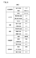
- Table 1 shows the state of the recess and the optical characteristics of Examples and Comparative Examples.
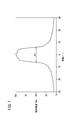
- Table 2 shows common conditions in Examples and Comparative Examples. It is a graph which shows the light distribution angle. It is a graph which shows the relationship between the diameter of a concave part and a light distribution angle. It is a graph which shows the relationship between the depth of a recess and a light distribution angle (and illuminance).
- the optical component 100 has at least one optical element 14 and a package 16.
- the optical element 14 emits light (for example, ultraviolet light), and the package 16 houses the optical element 14.
- the optical element 14 is, for example, an LED (light emitting diode) or LD (semiconductor laser). Although not shown, the optical element 14 can be configured by, for example, laminating a GaN-based crystal layer having a quantum well structure on a sapphire substrate.
- a so-called face-up mounting in which the crystal layer constituent surface 14a faces the light converging member 10 described later and functions as a light emitting surface can be adopted. That is, the terminal (not shown) derived from the optical element 14 and the circuit wiring (not shown) formed on the mounting substrate 18 are electrically connected by, for example, a bonding wire (not shown).
- a so-called flip-chip mounting in which the crystal layer constituent surface 14a is arranged on the bottom surface of the accommodation space 26 and the back surface of the sapphire substrate functions as a light emitting surface can also be adopted.
- Package 16 has a mounting board 18 and an optical converging member 10.
- the mounting substrate 18 is made of, for example, aluminum nitride, alumina, and aluminum, has an accommodation space 26, and accommodates the optical element 14 in the accommodation space 26.
- the accommodation space 26 has, for example, a cylindrical shape and a rectangular parallelepiped shape, and an optical element 14 is arranged on the bottom surface thereof.
- the light converging member 10 is fixed on the mounting substrate 18 and has a pedestal 28, a lens body 30, and a recess 32 as shown in FIGS. 1 and 2.
- quartz glass can be formed by, for example, a powder sintering method.
- the borosilicate glass, the silicone resin, and the fluororesin can be molded by, for example, press molding, injection molding, or machining.
- the light converging member 10 is joined onto the mounting substrate 18 via, for example, an organic or metal adhesive layer 20.
- an organic adhesive layer 20 for example, an epoxy-based adhesive, a silicone-based adhesive, a urethane-based adhesive, or the like can be used.
- an metal-based adhesive layer 20 for example, AuSn-based solder can be used.
- the pedestal 28 has an annular shape and is fixed on the mounting substrate 18.
- the outer shape (planar shape) of the pedestal 28 is, for example, a square shape.
- the outer shape of the pedestal 28 may be a polygonal shape such as a circular shape, a rectangular shape, a triangular shape, or a hexagonal shape.
- the light converging member 10 may be configured from the lens body 30 and the recess 32 without using the pedestal 28.
- the lens body 30 converges light and is integrally formed on the pedestal 28, and has, for example, an upwardly convex shape.
- the outer periphery of the lens body 30 can be formed to be continuously reduced as it is separated from the optical element 14. Further, the lens body 30 can have a curved surface shape that is symmetrical with respect to the central axis O.
- the outer surface of the lens body 30 does not have to be entirely curved. For example, it is permissible to make the vicinity of the top of the lens body 30 (a part of the upper surface intersecting the central axis O) a planar shape. This is because the light traveling along the central axis O has little need for convergence.
- the bottom surface 30a of the lens body 30 can be conceived at the boundary with the pedestal 28.
- the planar shape of the bottom surface 30a is, for example, a circular shape. However, the planar shape of the bottom surface 30a may be an elliptical shape, a track shape, or the like.
- the recess 32 is arranged so as to face the optical element 14, and as will be described later, supports the light convergence function of the lens body 30 and contributes to the improvement of the illuminance I and the reduction of the light distribution angle ⁇ f.
- the recess 32 is formed in the pedestal 28, but it may be formed in the lens body 30 as described later.
- the recess 32 has a dome shape, a columnar shape, a prismatic shape (for example, a triangular prism, a square prism, a prism shape having a pentagonal prism or more), a cone shape, and a prism shape (for example, a triangular prism, a square pyramid, or a prism shape having a pentagonal prism or more). ) And so on.
- a conical shape or a prismatic shape it is preferable to arrange the top of the cone or pyramid shape so that the top thereof is upward.
- the bottom surface of the recess 32 can have, for example, a plane close to the central axis O and a slope away from the central axis O. At this time, if the inclination of the bottom surface is continuously changed according to the distance from the central axis O, the recess 32 (bottom surface) becomes a dome shape.
- the dome shape include a hemispherical dome shape, a Low dome shape, and a Tall dome shape.
- the Low dome shape and the Tall dome shape are curved surfaces having an aspect ratio Rr smaller than 0.5 and larger than 0.5, respectively.
- Diameter Lr means the maximum length of the bottom surface of the recess 32. That is, if the shape of the bottom surface is circular, the diameter Lr means the diameter. If the shape of the bottom surface is triangular, the diameter Lr means the length of the side. If the shape of the bottom surface is a polygonal shape of a square or more, the diameter Lr means the length of the diagonal line (the maximum length connecting the vertices).
- the recesses 32 having various shapes, it is possible to support the light convergence function of the lens body 30 and contribute to the improvement of the illuminance I and the reduction of the light distribution angle ⁇ f.
- the light converging member 10 having such a shape can be manufactured by a powder sintering method, press molding, injection molding, or machining.
- a powder sintering method for example, a molding slurry containing quartz glass powder (silica powder) and an organic compound is cast into a molding die. This slurry is solidified by a chemical reaction between organic compounds, for example, a chemical reaction between a dispersion medium and a curing agent or a curing agent to obtain a molded product. The molded product is separated from the molding die and fired. In this way, the light focusing member 10 can be manufactured.
- the height hc of the light converging member 10 is, for example, 0.7 to 30 [mm].
- the outer diameter Da and height hl of the pedestal 28 are, for example, 3.0 to 100 [mm] and 0.2 to 1 [mm].
- the lens body 30 has a maximum diameter Lm, a maximum height hm, and an aspect ratio Rm, for example, 1 to 20 [mm], 0.5 to 30.0 [mm], and 0.3 to 1.5.
- the recess 32 has a diameter Lr, a depth hr, and an aspect ratio Rr, for example, 0.1 to 5.0 [mm], 0.1 to 5.0 [mm], and 0.1 to 1.0.
- the distance dr between the bottom surface 30a of the lens body 30 and the outer circumference of the recess 32 (here, the bottom surface of the pedestal 28) is, for example, 0 to 1.0 [mm].
- the optical element 14 has a substantially rectangular parallelepiped shape (for example, a rectangular parallelepiped shape, a shape in which the sides of the rectangular parallelepiped are chamfered), a substantially rectangular parallelepiped shape (for example, a rectangular parallelepiped shape (triangular column, hexagonal column, etc.), and a shape in which the sides of the rectangular parallelepiped are chamfered).
- the shape in the top view is a rectangle (square, rectangle), a shape obtained by chamfering a rectangle, a triangle, and a hexagon.
- the optical element 14 has a height (thickness) ht and a size Dt of, for example, 0.005 to 0.5 [mm] and 0.5 to 2.0 [mm].
- the size Dt means the maximum length of the light emitting region when the optical element 14 is viewed from above.
- the size Dt is the diagonal length (for example). It means the maximum length connecting the vertices).
- the distance dt between the upper surface of the optical element 14 (light emitting surface, crystal layer constituent surface 14a) and the outer circumference of the recess 32 (here, the bottom surface of the pedestal 28) is, for example, 0.05 to 1.0 [mm]. ..
- the mounting substrate 18 does not have the accommodation space 26.
- the recess 32 is used to support the light convergence function of the lens body 30 to improve the illuminance I and the light distribution angle ⁇ f, as in the embodiment. Can contribute to the reduction of.
- Both the examples and the comparative examples can be basically represented by FIG.
- the shape, diameter Lr, and depth hr of the recess 32 were changed as follows (see Table 1).
- Comparative Example 1 does not have a recess 32.
- the hemispherical dome shape has an aspect ratio Rr (hr / Lr) of 0.5, smaller than 0.5 for the low dome, and larger than 0.5 for the Tall dome.
- the diameters Lr of Comparative Examples 2 to 4 and Examples 1 to 11 are 0.3, 0.4, 0.5, 0.6, 0.7, 0.8, 0.9, 1.0, and 1.
- the ratio (Lr / Dt) to the size Dt of the optical element 14 at this time was changed to 1, 1.2, 1.6, 2.0, 2.4, 2.6 [mm]. .27, 0.35, 0.44, 0.53, 0.62, 0.71, 0.80, 0.88, 0.97, 1.06, 1.41, 1.77, 2.12 2.30).
- the diameter Lr of Examples 12 to 18 and Comparative Example 5 was set to 1.1 [mm] (ratio (Lr / Dt) was 0.97).
- the depth hrs of Examples 12 to 17 and Comparative Example 5 were 0.275, 0.4, 0.7, 0.825, 0.9, 0.95, and 1 [mm], respectively (the aspect ratio Rr was , 0.25, 0.36, 0.64, 0.75, 0.82, 0.86, 0.91).
- both Examples and Comparative Examples have the shapes shown in Table 2, and the material is made of quartz glass. That is, the light converging member 10 has a height hc of 2.47 [mm].
- the lens body 30 has a Tall lens shape, a maximum diameter Lm of 3.2 [mm], a maximum height hm of 1.97 [mm], and an aspect ratio Rm (hm / Lm) of 0.62.
- the concave portion 32 has a radius of curvature Ra of the outer circumference of 0.1 [mm], a distance dr of 0.5 [mm], and a distance dt of 0.4 [mm].
- the height hl of the pedestal 28 was 0.5 [mm], and the outer diameter Da was 3.5 [mm].
- the accommodation space 26 was arranged on the mounting substrate 18, and the shape was a cylinder, the outer diameter Dk was 2.5 [mm], and the height hk was 0.5 [mm].
- the optical element 14 is an LED chip, and has a rectangular parallelepiped shape (square shape when viewed from above), a size Dt of 1.1 [mm] (length of one side of the square shape: 0.8 [mm]), and a height ht of 0. It was set to 1 [mm].
- the light distribution distribution, light distribution angle ⁇ f, light extraction efficiency E, and illuminance I at the lens junction of the optical components according to the examples and comparative examples were confirmed by simulation (ray tracing method).
- Table 1 shows the light distribution angle ⁇ f, the light extraction efficiency E, and the illuminance I of the optical components according to the examples and the comparative examples.
- the light distribution angle ⁇ f refers to an angle width that is 1/2 of the maximum luminous intensity in the angular distribution of luminous intensity (see FIG. 7).
- the light extraction efficiency E refers to the ratio of the light output emitted to the outside of the optical component to the light output emitted from the LED chip.
- FIG. 8 is a graph showing the relationship between the diameter Lr of the recess 32 and the light distribution angle ⁇ f, and summarizes the results of Comparative Examples 1 to 4 and Examples 1 to 11.
- the diameter Lr of the recess 32 (size ratio with the optical element 14 (Lr / Dt)) has a great influence on the light distribution angle ⁇ f.
- the diameter Lr is preferably 0.55 to 1.6 [mm] (size ratio (Lr / Dt) is 0.5 to 1.5), and 0.6 to 1. It is more preferably 0 [mm] (size ratio (Lr / Dt) is 0.5 to 0.9).
- FIG. 9 is a graph showing the relationship between the depth hr of the recess 32 and the light distribution angle ⁇ f (and the illuminance I), and summarizes the results of Comparative Examples 1, 5, and Examples 6, 12 to 17.
- the depth hr is preferably 0.275 to 0.95 [mm] (aspect ratio Rr is 0.25 to 0.86), preferably 0.275 to 0.7 [mm] (aspect ratio Rr is 0.25 to 0.86). 0.64) is more preferable.
- the former range is exceeded, the light distribution angle ⁇ f becomes large, and when it is within the latter range, the illuminance / light distribution angle ratio (I / ⁇ f) can be increased (the light distribution angle ⁇ f is small and the illuminance I is large).
- the shape of the recess 32 is not limited to the hemispherical dome. Even in the case of a cylindrical shape, good results were obtained in both the light distribution angle ⁇ f and the light extraction efficiency E as compared with the case where there was no recess 32 (Comparative Example 1). That is, the recess 32 can have any shape of a hemispherical dome, a Low dome, a Tall dome, and a cylinder. Further, it can be inferred that even the prism, the cone, and the pyramid are better than the case where there is no recess 32 (Comparative Example 1).
- the light converging member 10 is useful for reducing the light distribution angle ⁇ f and improving the high illuminance I.
- the optical converging member (10) is used for an optical component (100) having an optical element (14) that emits light, faces the optical element (14), and faces the optical element (14). It includes a recess (32) having a size of 0.5 times or more the maximum length of the light emitting region in 14), and a lens body (30) that converges light that has passed through the recess (32).
- ⁇ f light distribution angle
- ⁇ f light distribution angle
- the recess (32) preferably has a size of 1.5 times or less the maximum length of the light emitting region in the optical element (14), and emits light in the optical element (14). It is more preferable that the size is 0.9 times or less the maximum length of the region. Thereby, the light distribution angle ( ⁇ f) can be further reduced.
- the ratio of the depth (hr) to the diameter (Lr) of the recess (32) is 0.25 to 0.86. If it deviates from this range, the light distribution angle ( ⁇ f) may increase.
- the ratio of the depth (hr) to the diameter (Lr) of the recess (32) is 0.25 to 0.64.
- the ratio (I / ⁇ f) of the illuminance (I) to the light distribution angle ( ⁇ f) can be increased (convergence of strong light (illuminance I) at a narrow light distribution angle ⁇ f).
- the aspect ratio (Rr) is smaller than 0.25, the light distribution angle ( ⁇ f) may be large, and when the aspect ratio (Rr) is larger than 0.64, the illuminance (I) may be small.
- the concave portion (32) has any shape of a dome shape, a cylinder, a prism, a cone, and a prism. Regardless of the shape, the light distribution angle ( ⁇ f) can be reduced.
- the recess (32) is preferably dome-shaped.
- the optical converging member (10) includes an annular pedestal (28) fixed on the mounting substrate (18) and integrally formed with the lens body (30). To do. This facilitates fixing to the mounting substrate (18).
- the optical converging member (10) has an accommodation space (26) for accommodating the optical element (14), and the recess (32) is the accommodation space (26). It is formed on the bottom surface.
- an inexpensive flat plate substrate can be used for the mounting substrate (18).
- the optical component (100) faces at least one optical element (14) that emits light and the optical element (14), and has a maximum light emitting region in the optical element (14). It includes a recess (32) having a size of 0.5 times or more the length and an optical converging member (10) having a lens body (30) that converges light that has passed through the recess (32). Thereby, the light distribution angle ( ⁇ f) can be reduced.
- optical focusing member and the optical component according to the present invention are not limited to the above-described embodiments, and various configurations can be adopted without departing from the gist of the present invention.
Landscapes
- Engineering & Computer Science (AREA)
- General Engineering & Computer Science (AREA)
- Physics & Mathematics (AREA)
- General Physics & Mathematics (AREA)
- Optics & Photonics (AREA)
- Lenses (AREA)
- Led Device Packages (AREA)
- Semiconductor Lasers (AREA)
Priority Applications (3)
| Application Number | Priority Date | Filing Date | Title |
|---|---|---|---|
| JP2021563861A JPWO2021117530A1 (https=) | 2019-12-10 | 2020-11-30 | |
| US17/805,502 US11828452B2 (en) | 2019-12-10 | 2022-06-06 | Light converging member and optical component |
| JP2023135137A JP7695307B2 (ja) | 2019-12-10 | 2023-08-23 | 光収束部材および光学部品 |
Applications Claiming Priority (2)
| Application Number | Priority Date | Filing Date | Title |
|---|---|---|---|
| JP2019-222658 | 2019-12-10 | ||
| JP2019222658 | 2019-12-10 |
Related Child Applications (1)
| Application Number | Title | Priority Date | Filing Date |
|---|---|---|---|
| US17/805,502 Continuation US11828452B2 (en) | 2019-12-10 | 2022-06-06 | Light converging member and optical component |
Publications (1)
| Publication Number | Publication Date |
|---|---|
| WO2021117530A1 true WO2021117530A1 (ja) | 2021-06-17 |
Family
ID=76330184
Family Applications (1)
| Application Number | Title | Priority Date | Filing Date |
|---|---|---|---|
| PCT/JP2020/044428 Ceased WO2021117530A1 (ja) | 2019-12-10 | 2020-11-30 | 光収束部材および光学部品 |
Country Status (3)
| Country | Link |
|---|---|
| US (1) | US11828452B2 (https=) |
| JP (2) | JPWO2021117530A1 (https=) |
| WO (1) | WO2021117530A1 (https=) |
Citations (3)
| Publication number | Priority date | Publication date | Assignee | Title |
|---|---|---|---|---|
| JP2014130212A (ja) * | 2012-12-28 | 2014-07-10 | Konica Minolta Inc | 光学素子及び照明装置 |
| JP2017162662A (ja) * | 2016-03-09 | 2017-09-14 | 株式会社エンプラス | 発光装置および面光源装置 |
| JP2019511127A (ja) * | 2016-03-23 | 2019-04-18 | エルジー イノテック カンパニー リミテッド | 光学モジュール |
Family Cites Families (4)
| Publication number | Priority date | Publication date | Assignee | Title |
|---|---|---|---|---|
| JP6106872B2 (ja) | 2012-09-01 | 2017-04-05 | ラボ・スフィア株式会社 | バルク型レンズ及びそれを用いた発光体並びに照明装置 |
| JP6413759B2 (ja) | 2014-12-25 | 2018-10-31 | 株式会社島津製作所 | 光学分析装置 |
| CN107850822A (zh) * | 2015-08-20 | 2018-03-27 | 松下知识产权经营株式会社 | 照明装置、摄像装置以及透镜 |
| US10697612B2 (en) * | 2018-05-02 | 2020-06-30 | Frank Shum | Light distribution for planar photonic component |
-
2020
- 2020-11-30 JP JP2021563861A patent/JPWO2021117530A1/ja active Pending
- 2020-11-30 WO PCT/JP2020/044428 patent/WO2021117530A1/ja not_active Ceased
-
2022
- 2022-06-06 US US17/805,502 patent/US11828452B2/en active Active
-
2023
- 2023-08-23 JP JP2023135137A patent/JP7695307B2/ja active Active
Patent Citations (3)
| Publication number | Priority date | Publication date | Assignee | Title |
|---|---|---|---|---|
| JP2014130212A (ja) * | 2012-12-28 | 2014-07-10 | Konica Minolta Inc | 光学素子及び照明装置 |
| JP2017162662A (ja) * | 2016-03-09 | 2017-09-14 | 株式会社エンプラス | 発光装置および面光源装置 |
| JP2019511127A (ja) * | 2016-03-23 | 2019-04-18 | エルジー イノテック カンパニー リミテッド | 光学モジュール |
Also Published As
| Publication number | Publication date |
|---|---|
| US20220299188A1 (en) | 2022-09-22 |
| JP7695307B2 (ja) | 2025-06-18 |
| US11828452B2 (en) | 2023-11-28 |
| JP2023169160A (ja) | 2023-11-29 |
| JPWO2021117530A1 (https=) | 2021-06-17 |
Similar Documents
| Publication | Publication Date | Title |
|---|---|---|
| US11201271B2 (en) | Method for manufacturing light emitting device including first and second reflectors | |
| JP7221984B2 (ja) | 透明封止部材及び光学部品 | |
| US10381507B2 (en) | Light emitting diode chip and a method for the manufacture of a light emitting diode chip | |
| US20100165635A1 (en) | Led unit | |
| CN101297153B (zh) | 多件式反射角变换器 | |
| CN101971376A (zh) | 半导体装置 | |
| US20200192003A1 (en) | Optical component and transparent sealing member | |
| JPWO2018100775A1 (ja) | 光学部品及び透明体 | |
| TWI674683B (zh) | 封裝具有底部反射器的發光二極體透鏡 | |
| CN101997076A (zh) | 发光二极管封装体 | |
| US9997681B2 (en) | Lens and light emitting diode package including same | |
| JP7695307B2 (ja) | 光収束部材および光学部品 | |
| JP2016111179A (ja) | 発光装置 | |
| TW201316566A (zh) | 發光模組及其發光裝置 | |
| KR20160147576A (ko) | 발광 소자 패키지 | |
| US20120068212A1 (en) | Light-emitting device | |
| KR20150092597A (ko) | 발광 소자 패키지 및 이를 포함하는 조명 장치 | |
| KR100996918B1 (ko) | 전자부품 패키지 | |
| TWI458137B (zh) | 發光二極體封裝結構 | |
| KR101662308B1 (ko) | Led용 렌즈 및 그것을 포함하는 발광장치 | |
| KR20180101288A (ko) | 컨벡스 칩 스케일 패키지 및 그의 제조 방법 | |
| CN117317104A (zh) | 发光二极管芯片的封装结构及应用 | |
| CN205542882U (zh) | 发光二极管封装体 | |
| JP2024176656A (ja) | 発光装置 | |
| CN117461152A (zh) | 发光装置 |
Legal Events
| Date | Code | Title | Description |
|---|---|---|---|
| 121 | Ep: the epo has been informed by wipo that ep was designated in this application |
Ref document number: 20898618 Country of ref document: EP Kind code of ref document: A1 |
|
| ENP | Entry into the national phase |
Ref document number: 2021563861 Country of ref document: JP Kind code of ref document: A |
|
| NENP | Non-entry into the national phase |
Ref country code: DE |
|
| 122 | Ep: pct application non-entry in european phase |
Ref document number: 20898618 Country of ref document: EP Kind code of ref document: A1 |