WO2021111994A1 - 基準電圧生成回路 - Google Patents
基準電圧生成回路 Download PDFInfo
- Publication number
- WO2021111994A1 WO2021111994A1 PCT/JP2020/044149 JP2020044149W WO2021111994A1 WO 2021111994 A1 WO2021111994 A1 WO 2021111994A1 JP 2020044149 W JP2020044149 W JP 2020044149W WO 2021111994 A1 WO2021111994 A1 WO 2021111994A1
- Authority
- WO
- WIPO (PCT)
- Prior art keywords
- reference voltage
- transistor
- voltage
- generation circuit
- voltage generation
- Prior art date
- Legal status (The legal status is an assumption and is not a legal conclusion. Google has not performed a legal analysis and makes no representation as to the accuracy of the status listed.)
- Ceased
Links
Images


Classifications
-
- G—PHYSICS
- G05—CONTROLLING; REGULATING
- G05F—SYSTEMS FOR REGULATING ELECTRIC OR MAGNETIC VARIABLES
- G05F1/00—Automatic systems in which deviations of an electric quantity from one or more predetermined values are detected at the output of the system and fed back to a device within the system to restore the detected quantity to its predetermined value or values, i.e. retroactive systems
- G05F1/10—Regulating voltage or current
- G05F1/46—Regulating voltage or current wherein the variable actually regulated by the final control device is DC
- G05F1/468—Regulating voltage or current wherein the variable actually regulated by the final control device is DC characterised by reference voltage circuitry, e.g. soft start, remote shutdown
-
- G—PHYSICS
- G05—CONTROLLING; REGULATING
- G05F—SYSTEMS FOR REGULATING ELECTRIC OR MAGNETIC VARIABLES
- G05F3/00—Non-retroactive systems for regulating electric variables by using an uncontrolled element, or an uncontrolled combination of elements, such element or such combination having self-regulating properties
- G05F3/02—Regulating voltage or current
- G05F3/08—Regulating voltage or current wherein the variable is DC
- G05F3/10—Regulating voltage or current wherein the variable is DC using uncontrolled devices with non-linear characteristics
- G05F3/16—Regulating voltage or current wherein the variable is DC using uncontrolled devices with non-linear characteristics being semiconductor devices
- G05F3/20—Regulating voltage or current wherein the variable is DC using uncontrolled devices with non-linear characteristics being semiconductor devices using diode- transistor combinations
- G05F3/30—Regulators using the difference between the base-emitter voltages of two bipolar transistors operating at different current densities
-
- H—ELECTRICITY
- H02—GENERATION; CONVERSION OR DISTRIBUTION OF ELECTRIC POWER
- H02M—APPARATUS FOR CONVERSION BETWEEN AC AND AC, BETWEEN AC AND DC, OR BETWEEN DC AND DC, AND FOR USE WITH MAINS OR SIMILAR POWER SUPPLY SYSTEMS; CONVERSION OF DC OR AC INPUT POWER INTO SURGE OUTPUT POWER; CONTROL OR REGULATION THEREOF
- H02M3/00—Conversion of DC power input into DC power output
- H02M3/02—Conversion of DC power input into DC power output without intermediate conversion into AC
- H02M3/04—Conversion of DC power input into DC power output without intermediate conversion into AC by static converters
- H02M3/10—Conversion of DC power input into DC power output without intermediate conversion into AC by static converters using discharge tubes with control electrode or semiconductor devices with control electrode
- H02M3/145—Conversion of DC power input into DC power output without intermediate conversion into AC by static converters using discharge tubes with control electrode or semiconductor devices with control electrode using devices of a triode or transistor type requiring continuous application of a control signal
- H02M3/155—Conversion of DC power input into DC power output without intermediate conversion into AC by static converters using discharge tubes with control electrode or semiconductor devices with control electrode using devices of a triode or transistor type requiring continuous application of a control signal using semiconductor devices only
- H02M3/156—Conversion of DC power input into DC power output without intermediate conversion into AC by static converters using discharge tubes with control electrode or semiconductor devices with control electrode using devices of a triode or transistor type requiring continuous application of a control signal using semiconductor devices only with automatic control of output voltage or current, e.g. switching regulators
- H02M3/158—Conversion of DC power input into DC power output without intermediate conversion into AC by static converters using discharge tubes with control electrode or semiconductor devices with control electrode using devices of a triode or transistor type requiring continuous application of a control signal using semiconductor devices only with automatic control of output voltage or current, e.g. switching regulators including plural semiconductor devices as final control devices for a single load
Definitions
- the present invention relates to a reference voltage generation circuit that generates a reference voltage.
- a reference voltage generation circuit called a bandgap reference circuit is known (see, for example, Patent Document 1).
- the reference voltage generated by the reference voltage generation circuit disclosed in Patent Document 1 is a voltage based on the ground voltage and is a voltage determined by the bandgap reference voltage.
- the bandgap reference voltage is a reference voltage obtained by using the bandgap voltage of the semiconductor.
- the power transistor is an NDMOS transistor (N-type double diffusion MOS transistor)
- the voltage itself applied to the HVNW is the power. Since it becomes the output voltage of the transistor, the voltage applied to the HVNW fluctuates due to the switching of the power transistor. Then, the voltage fluctuation propagates as noise by capacitive coupling.
- the power transistor is an NDMOS transistor, for example, the voltage itself applied to the HVNW by the regenerative current becomes a negative voltage. When this happens, the parasitic collector current of the parasitic transistor PTR will flow.
- the reference voltage generation circuit disclosed in Patent Document 1 has a configuration in which the HVNW corresponding to the back gate of the differential pair transistor in the amplifier and the HVNW corresponding to the anode of the diode are not connected to the power supply voltage. It was.
- the reference voltage generation circuit disclosed in the present specification includes a bandgap reference circuit that generates a first reference voltage that depends on a bandgap reference voltage and a power supply voltage, and converts the first reference voltage into a second reference voltage.
- the second reference voltage depends on the bandgap reference voltage and the ground voltage, and the ground voltage is lower than the power supply voltage (first configuration).
- the conversion circuit includes an amplifier, and the output end of the bandgap reference circuit and the first input end of the amplifier are connected without a resistance element (first configuration). 2 configuration) may be used.
- the conversion circuit includes a first transistor provided between a first application end to which the power supply voltage is applied and a second input end of the amplifier, and the amplifier.
- a second transistor provided between the second input end and the second application end to which the ground voltage is applied is further provided, and the control end of the first transistor is connected to the first application end.
- the second reference voltage or the divided voltage of the second reference voltage may be supplied to the control end of the second transistor (third configuration).
- the gate length of the first transistor and the gate length of the second transistor may be longer than the gate length of the transistor inside the amplifier (fourth configuration).
- the gate length of the first transistor and the gate length of the second transistor may each be 5 ⁇ m or more (fifth configuration).
- the gate length of the first transistor and the gate length of the second transistor may be substantially the same (sixth configuration).
- the conversion circuit further includes a third transistor provided between the second input end of the amplifier and the second transistor, and the conversion circuit further includes a third transistor.
- a configuration in which a bias voltage is supplied to the control end of the third transistor may be used.
- the semiconductor device disclosed in the present specification has a configuration (eighth configuration) including a reference voltage generation circuit having any of the first to seventh configurations described above.
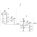
- FIG. 1 The figure which shows the reference voltage generation circuit which concerns on one Embodiment
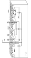
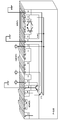
- Cross-sectional perspective view schematically showing a structural example of a semiconductor device Cross-sectional perspective view schematically showing a structural example of a semiconductor device
- a MOS transistor is a semiconductor whose gate structure is "a layer made of a semiconductor such as a conductor or polysilicon having a small resistance value", an “insulating layer”, and a "P-type, N-type, or intrinsic semiconductor".
- a field effect transistor consisting of at least three layers of "layers”. That is, the gate structure of the MOS transistor is not limited to the three-layer structure of metal, oxide, and semiconductor.
- the reference voltage means a voltage that is constant in an ideal state, and is actually a voltage that can fluctuate slightly due to a temperature change or the like.
- FIG. 1 is a diagram showing a reference voltage generation circuit according to an embodiment.
- the reference voltage generation circuit 1 includes a bandgap reference circuit 2 and a conversion circuit 3.
- the bandgap reference circuit 2 generates the first reference voltage VREF1.
- the first reference voltage VREF1 depends on the bandgap reference voltage and the power supply voltage VCS.
- the first reference voltage VREF1 is a voltage with reference to the power supply voltage VCS, and is a voltage determined by the bandgap reference voltage.
- the bandgap reference voltage is a reference voltage obtained by using the bandgap voltage of the semiconductor.
- the conversion circuit 3 converts the first reference voltage VREF1 into the second reference voltage VREF2.
- the second reference voltage VREF2 depends on the bandgap reference voltage and the ground voltage VSS.
- the second reference voltage VREF2 is a voltage with reference to the ground voltage VSS, and is a voltage determined by the bandgap reference voltage.
- the ground voltage VSS is a voltage lower than the power supply voltage VCS.
- the bandgap reference circuit 2 is configured to generate the first reference voltage VREF1 based on the power supply voltage VCS. Therefore, all HVNWs used to form the bandgap reference circuit 2 can be connected to the power supply voltage VCS. As a result, adverse effects due to noise and parasitic current can be avoided.
- the reference voltage generation circuit 1 includes the conversion circuit 3, it is possible to generate the second reference voltage VREF2, which is a voltage based on the ground voltage VSS, while avoiding adverse effects due to noise and parasitic current. Since the second reference voltage VREF2 is a voltage based on the ground voltage VSS, it can be widely used in other circuits without limitation.
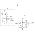
- FIG. 2 is a diagram showing a first configuration example of the reference voltage generation circuit 1.
- the reference voltage generation circuit 1A which is the first configuration example of the reference voltage generation circuit 1, includes a bandgap reference circuit 2A and a conversion circuit 3A.
- the bandgap reference circuit 2A is an example of the bandgap reference circuit 2 in FIG. 1
- the conversion circuit 3A is an example of the conversion circuit 3 in FIG.
- the bandgap reference circuit 2A includes resistors R1 to R3 (all are poly resistors), NPN bipolar transistors Q1 and Q2, and an operational amplifier AMP1.
- the NPN bipolar transistors Q1 and Q2 are diode-connected and function as diodes.
- the first power supply end of the operational amplifier AMP1 is connected to the application end of the power supply voltage VCS.
- the second power supply end of the operational amplifier AMP1 is connected to the application end of the ground voltage VSS.
- Both the first end of the resistor R1 and the first end of the resistor R2 are connected to the output end of the operational amplifier AMP1.
- Both the second end of the resistor R1 and the emitter of the NPN bipolar transistor Q1 are connected to the non-inverting input end (+) of the operational amplifier AMP1.
- Both the second end of the resistor R2 and the first end of the resistor R3 are connected to the inverting input end ( ⁇ ) of the operational amplifier AMP1.
- the second end of the resistor R3 is connected to the emitter of the NPN bipolar transistor Q2.
- the base and collector of each of the NPN bipolar transistors Q1 and Q2 are connected to the application end of the power supply voltage VCS.
- the output end of the operational amplifier AMP1 is the output end of the bandgap reference circuit 2A.
- the first reference voltage VREF1 is output from the output end of the operational amplifier AMP1.
- the conversion circuit 3A includes resistors R11 to R14 (all are poly resistors), an N-channel type MOS transistor Q11, and an operational amplifier AMP11.
- the conversion circuit 3A is a differential amplifier circuit using the operational amplifier AMP11.
- the first power supply end of the operational amplifier AMP11 is connected to the application end of the power supply voltage VCS.
- the second power supply end of the operational amplifier AMP11 is connected to the application end of the ground voltage VSS.
- the first end of the resistor R11 is the input end of the conversion circuit 3A, and the first reference voltage VREF1 is supplied. Both the second end of the resistor R11 and the first end of the resistor R12 are connected to the inverting input end ( ⁇ ) of the operational amplifier AMP11. The second end of the resistor R12 is connected to the output end of the operational amplifier AMP11. The first end of the resistor R13 is connected to the application end of the power supply voltage VCS. Both the second end of the resistor R13 and the first end of the resistor R14 are connected to the non-inverting input end (+) of the operational amplifier AMP11. The second end of the resistor R14 is connected to the drain of the N-channel type MOS transistor Q11.
- the source and back gate of the N-channel type MOS transistor Q11 are connected to the application end of the ground voltage VSS.
- a gate voltage VSW which is a signal for switching on / off of the N-channel type MOS transistor Q11, is supplied to the gate of the N-channel type MOS transistor Q11. By turning off the N-channel type MOS transistor Q11, the steady current of the conversion circuit 3A can be cut.
- the output end of the operational amplifier AMP11 is the output end of the reference voltage generation circuit 1A.
- the second reference voltage VREF2 is output from the output end of the operational amplifier AMP11.
- the second reference voltage VREF2 output from the reference voltage generation circuit 1A is the following equation (1). It is represented by.
- the BGR in the equation (1) is a bandgap reference voltage. VREF2 ⁇ BGR ⁇ r2 / r1 ... (1)
- a resistor R11 is provided between the output end of the bandgap reference circuit 2A and the inverting input end (-) of the operational amplifier AMP11. That is, since the resistor R11 through which the current flows is provided as the load to which the bandgap reference voltage BGR is supplied, the reference voltage generation circuit 1A is a circuit that has room for improvement from the viewpoint of current consumption.
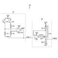
- FIG. 3 is a diagram showing a second configuration example of the reference voltage generation circuit 1.
- the reference voltage generation circuit 1B which is a second configuration example of the reference voltage generation circuit 1, includes a bandgap reference circuit 2A and a conversion circuit 3B.
- the conversion circuit 3B is also an example of the conversion circuit 3 in FIG. 1 in the same manner as the conversion circuit 3A described above.
- the conversion circuit 3B includes an operational amplifier AMP21, resistors R21 and R22 (both are poly resistors), and a P-channel type MOS transistor Q21.
- the first power supply end of the operational amplifier AMP21 is connected to the application end of the power supply voltage VCS.
- the second power supply end of the operational amplifier AMP21 is connected to the application end of the ground voltage VSS.
- the non-inverting input end (+) of the operational amplifier AMP21 is the input end of the conversion circuit 3B, and the first reference voltage VREF1 is supplied.
- the output end of the operational amplifier AMP21 is connected to the gate of the P-channel type MOS transistor Q21.
- the first end of the resistor R21 is connected to the application end of the power supply voltage VCS and the back gate of the P-channel type MOS transistor Q21.
- the second end of the resistor R21 is connected to the inverting input end ( ⁇ ) of the operational amplifier AMP21 and the source of the P-channel type MOS transistor Q21.
- the drain of the P-channel type MOS transistor Q21 is connected to the first end of the resistor R22.
- the second end of resistor R22 is connected to the ground voltage VSS.
- connection node between the drain of the P-channel type MOS transistor Q21 and the first end of the resistor R22 is the output end of the reference voltage generation circuit 1B.
- the second reference voltage VREF2 is output from the connection node between the drain of the P-channel type MOS transistor Q21 and the first end of the resistor R22.
- the first reference voltage VREF1 is supplied to the second end of the resistor R21, and the potential difference between both ends of the resistor R21 becomes the bandgap reference voltage. Therefore, the value of the current flowing through the resistor R21 is the value obtained by dividing the bandgap reference voltage by the resistance value of the resistor R21. Therefore, assuming that the resistance value of the resistor R21 is r1 and the resistance value of the resistor R22 is r2, the second reference voltage VREF2 output from the reference voltage generation circuit 1B is represented by the following equation (2).
- the BGR in the equation (2) is the bandgap reference voltage
- the ISUB is the current flowing through the substrate.
- the reference voltage generation circuit 1B is a circuit that has room for improvement from the viewpoint of temperature characteristics because the second reference voltage VREF2 is affected by the current ISUB flowing through the substrate.
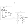
- FIG. 4 is a diagram showing a third configuration example of the reference voltage generation circuit 1.
- the reference voltage generation circuit 1C which is a third configuration example of the reference voltage generation circuit 1, includes a bandgap reference circuit 2A and a conversion circuit 3A.
- the conversion circuit 3C is also an example of the conversion circuit 3 in FIG. 1 in the same manner as the conversion circuits 3A and 3B described above.
- the conversion circuit 3C includes N-channel type MOS transistors Q31 and Q32, an operational amplifier AMP31, and resistors R31 and R32 (both are poly resistors).
- the first power supply end of the operational amplifier AMP31 is connected to the application end of the power supply voltage VCS.
- the second power supply end of the operational amplifier AMP31 is connected to the application end of the ground voltage VSS.
- the inverting input end (-) of the operational amplifier AMP31 is the input end of the conversion circuit 3C, and the first reference voltage VREF1 is supplied.
- the drain and gate of the N-channel MOS transistor Q31 are connected to the application end of the power supply voltage VCS.
- the source and back gate of the N-channel MOS transistor Q31 and the drain of the N-channel MOS transistor Q32 are connected to the non-inverting input end (+) of the operational amplifier AMP31.
- the source and back gate of the N-channel type MOS transistor Q32 are connected to the ground voltage VSS.
- the output end of the operational amplifier AMP31 is the output end of the reference voltage generation circuit 1C.
- the second reference voltage VREF2 is output from the output end of the operational amplifier AMP31.
- the output end of the operational amplifier AMP31 is connected to the first end of the resistor R31.
- the second end of the resistor R31 is connected to the first end of the resistor R32 and the gate of the N-channel type MOS transistor Q32.
- the second end of resistor R32 is connected to the ground voltage VSS.
- the output end of the MOSFET AMP31 may be directly connected to the gate of the N-channel MOS transistor Q32 without providing the resistor r31 and the resistor R32. That is, the second reference voltage VREF2 may be supplied to the gate of the N-channel type MOS transistor Q32 instead of dividing the second reference voltage VREF2.
- the drain current of the N-channel type MOS transistor Q31 and the drain current of the N-channel type MOS transistor Q32 are the same.
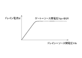
- the N-channel type MOS transistors Q31 and Q32 have the characteristics shown in FIG. That is, if the gate-source voltage of the N-channel MOS transistor is constant in each of the N-channel MOS transistors Q31 and Q32, N will occur in the saturation region regardless of the drain-source voltage of the N-channel MOS transistor Q32.
- the drain current of the channel type MOS transistor is made to be substantially constant, and the N channel type MOS transistors Q31 and Q32 are made to have substantially the same characteristics. As a result, the equation (3) described later is established.
- the channel lengths of the N-channel MOS transistors Q31 and Q32 are lengthened so that the N-channel MOS transistors Q31 and Q32 both have the characteristics shown in FIG. 4, and the shapes of the N-channel MOS transistors Q31 and Q32 are substantially the same. ing.
- the channel lengths of the N-channel type MOS transistors Q31 and Q32 may be longer than the gate length of the transistors inside the operational amplifier AMP31.
- the second reference voltage VREF2 for example, if the gate lengths of the N-channel MOS transistors Q31 and Q32 are set to 5 ⁇ m or more, the drain currents of the N-channel MOS transistors Q31 and Q32 will increase in the saturation region. The degree of constant constant becomes good, and the accuracy of the second reference voltage VREF2 becomes good.
- the gate length of the N-channel type MOS transistor Q31 and the gate length of the N-channel type MOS transistor Q32 may be substantially the same.
- the first reference voltage VREF1 is supplied to the source of the N-channel type MOS transistor Q31, and the gate-source voltage of the N-channel type MOS transistor Q31 becomes the band gap reference voltage.
- the gate-source voltage of the N-channel type MOS transistor Q31 becomes a divided voltage of the second reference voltage VREF2. Therefore, assuming that the resistance value of the resistor R31 is r1 and the resistance value of the resistor R32 is r2, the second reference voltage VREF2 output from the reference voltage generation circuit 1C is represented by the following equation (3).
- the BGR in the equation (3) is a bandgap reference voltage. VREF2 ⁇ BGR ⁇ (r1 + r2) / r2 ... (3)
- FIG. 6 is a diagram showing a fourth configuration example of the reference voltage generation circuit 1.
- the reference voltage generation circuit 1D which is the fourth configuration example of the reference voltage generation circuit 1, includes a bandgap reference circuit 2A and a conversion circuit 3D.
- the conversion circuit 3D is also an example of the conversion circuit 3 in FIG. 1 in the same manner as the conversion circuits 3A to 3C described above.
- the conversion circuit 3D in FIG. 6 has a configuration in which an N-channel type MOS transistor Q33 is added to the conversion circuit 3C in FIG.
- the N-channel type MOS transistor Q33 is provided between the N-channel type MOS transistor Q31 and the N-channel type MOS transistor Q32.
- the drain of the N-channel type MOS transistor Q33 is connected to the source and back gate of the N-channel type MOS transistor Q31 and the non-inverting input end (+) of the operational amplifier AMP31.
- the source and back gate of the N-channel type MOS transistor Q33 are connected to the drain of the N-channel type MOS transistor Q32.
- a predetermined bias voltage VB is supplied to the gate of the N-channel type MOS transistor Q33.
- the conversion circuit 3D in FIG. 6 can suppress fluctuations in the drain-source voltage of each of the N-channel type MOS transistors Q31 and Q32 even when the power supply voltage VCS fluctuates. .. Therefore, the reference voltage generation circuit 1D shown in FIG. 6 has improved stability of the second reference voltage VREF2 as compared with the reference voltage generation circuit 1C shown in FIG.
- the conversion circuit 3D in FIG. 6 can suppress fluctuations in the drain-source voltage of each of the N-channel type MOS transistors Q31 and Q32 even when the power supply voltage VCS fluctuates. Therefore, although it depends on the required accuracy of the second reference voltage VREF2, the reference voltage generation circuit 1D shown in FIG. 6 can be configured so that the channel lengths of the N-channel type MOS transistors Q31 and Q32 are not lengthened. ..
- FIG. 7 (a) to 7 (c) are block diagrams showing each example of a semiconductor device including the reference voltage generation circuit 1.
- the semiconductor device 10A of FIG. 7A includes at least one of a D / A converter 11 and an A / D converter 12 in addition to the reference voltage generation circuit 1.
- the D / A converter 11 converts the digital signal DIN into an analog voltage VOUT.
- the second reference voltage VREF2 output from the reference voltage generation circuit 1 is supplied to the reference voltage terminal of the D / A converter 11.
- the A / D converter 12 converts the analog voltage VIN into a digital signal DOUT.
- the second reference voltage VREF2 output from the reference voltage generation circuit 1 is supplied to the reference voltage terminal of the A / D converter 12.
- Examples of the semiconductor device 10A include DSPs (digital signal processing devices) for audio and other applications, microcomputers, ASICs (Application Specified ICs), FPGAs (Field Programmable Gate Arrays), and the like.
- the semiconductor device 10B of FIG. 7B is a control circuit of a DC / DC converter.
- the semiconductor device 10B includes an error amplifier 13, a pulse modulator 14, and a driver 15 in addition to the reference voltage generation circuit 1.
- the error amplifier 13 outputs an error voltage VERR which is a voltage obtained by amplifying the error between the feedback voltage VFB corresponding to the output voltage of the DC / DC converter and the second reference voltage VREF2.
- the pulse modulator 14 generates a pulse signal SPWM having a duty ratio corresponding to the error voltage VERR output from the error amplifier 13.
- the driver 15 drives a switching transistor (not shown) of the DC / DC converter based on the pulse signal SPWM.
- the topology and control method of the DC / DC converter are not limited.
- the semiconductor device 10B may include at least one of a circuit that generates a feedback voltage VFB and a switching transistor.
- the semiconductor device 10C of FIG. 7C is a control circuit of a linear regulator.
- the semiconductor device 10C includes an error amplifier 16, an output transistor 17, and voltage dividing resistors 18 and 19 in addition to the reference voltage generation circuit 1.
- the voltage dividing resistors 18 and 19 generate a feedback voltage VFB corresponding to the output voltage of the linear regulator.
- the error amplifier 16 outputs an error voltage VERR which is a voltage obtained by amplifying the error between the feedback voltage VFB corresponding to the output voltage of the linear regulator and the second reference voltage VREF2.
- the output transistor 17 is driven according to the error voltage VERR.
- At least one of the circuit (voltage dividing resistors 18 and 19) for generating the feedback voltage VFB and the output transistor 19 may be provided outside the semiconductor device 10C.
- the reference voltage generation circuit 1 can be used in various semiconductor devices.
- each circuit element constituting the reference voltage generation circuit 1 is preferably formed inside an N-type well to which the power supply voltage VCS is applied. As a result, it is possible to prevent the bandgap reference voltage from fluctuating when the power supply voltage VCS fluctuates.
Landscapes
- Engineering & Computer Science (AREA)
- Physics & Mathematics (AREA)
- Power Engineering (AREA)
- Electromagnetism (AREA)
- General Physics & Mathematics (AREA)
- Radar, Positioning & Navigation (AREA)
- Automation & Control Theory (AREA)
- Microelectronics & Electronic Packaging (AREA)
- Nonlinear Science (AREA)
- Control Of Electrical Variables (AREA)
- Semiconductor Integrated Circuits (AREA)
Abstract
基準電圧生成回路(1)は、バンドギャップ基準電圧及び電源電圧(VCC)に依存する第1基準電圧(VREF1)を生成するバンドギャップリファレンス回路(2)と、前記第1基準電圧を第2基準電圧(VREF2)に変換する変換回路(3)と、を備える。前記第2基準電圧は前記バンドギャップ基準電圧及び接地電圧(VSS)に依存する。前記接地電圧は前記電源電圧より低い。
Description
本発明は、基準電圧を生成する基準電圧生成回路に関する。
従来、バンドギャップリファレンス回路と呼ばれる基準電圧生成回路が知られている(例えば特許文献1参照)。特許文献1で開示されている基準電圧生成回路によって生成される基準電圧は、接地電圧を基準とする電圧であって、バンドギャップ基準電圧によって定まる電圧である。なお、バンドギャップ基準電圧は、半導体のバンドギャップ電圧を利用して得られる基準電圧である。
ここで、図8に示す構造の半導体装置を考えた場合、パワートランジスタがNDMOSトランジスタ(N型2重拡散MOSトランジスタ)であれば、HVNW(高電圧N型ウェル)に印加される電圧そのものがパワートランジスタの出力電圧になるため、パワートランジスタのスイッチングによりHVNWに印加される電圧が変動する。そして、その電圧変動が容量結合によってノイズとして伝搬する。
また、図9に示す構造の半導体装置(=図8に示す構造の半導体装置)を考えた場合、パワートランジスタがNDMOSトランジスタであれば、例えば回生電流によってHVNWに印加される電圧そのものが負電圧になったときに、寄生トランジスタPTRの寄生コレクタ電流が流れてしまう。
基準電圧生成回路に上述したノイズや寄生電流による悪影響が及ばないようにするためには、全てのHVNWに電源電圧を印加する必要がある。しかしながら、特許文献1で開示されている基準電圧生成回路は、アンプ内の差動対トランジスタのバックゲートに対応するHVNWとダイオードのアノードに対応するHVNWとが電源電圧に接続されていない構成であった。
本明細書中に開示されている基準電圧生成回路は、バンドギャップ基準電圧及び電源電圧に依存する第1基準電圧を生成するバンドギャップリファレンス回路と、前記第1基準電圧を第2基準電圧に変換する変換回路と、を備え、前記第2基準電圧は前記バンドギャップ基準電圧及び接地電圧に依存し、前記接地電圧は前記電源電圧より低い構成(第1の構成)である。
上記第1の構成の基準電圧生成回路において、前記変換回路はアンプを備え、前記バンドギャップリファレンス回路の出力端と前記アンプの第1入力端とが抵抗素子を介さずに接続される構成(第2の構成)としてもよい。
上記第2の構成の基準電圧生成回路において、前記変換回路は、前記電源電圧が印加される第1印加端と前記アンプの第2入力端との間に設けられる第1トランジスタと、前記アンプの前記第2入力端と前記接地電圧が印加される第2印加端との間に設けられる第2トランジスタと、をさらに備え、前記第1トランジスタの制御端が前記第1印加端に接続され、前記第2基準電圧又は前記第2基準電圧の分圧が前記第2トランジスタの制御端に供給される構成(第3の構成)としてもよい。
上記第3の構成の基準電圧生成回路において、前記第1トランジスタのゲート長及び前記第2トランジスタのゲート長は、前記アンプ内部のトランジスタのゲート長より長い構成(第4の構成)としてもよい。
上記第4の構成の基準電圧生成回路において、前記第1トランジスタのゲート長及び前記第2トランジスタのゲート長はそれぞれ5μm以上である構成(第5の構成)としてもよい。
上記第4又は第5の構成の基準電圧生成回路において、前記第1トランジスタのゲート長と前記第2トランジスタのゲート長とは、略同一である構成(第6の構成)としてもよい。
上記第3~第6のいずれかの構成の基準電圧生成回路において、前記変換回路は、前記アンプの前記第2入力端と前記第2トランジスタとの間に設けられる第3トランジスタをさらに備え、前記第3トランジスタの制御端にバイアス電圧が供給される構成(第7の構成)としてもよい。
本明細書中に開示されている半導体装置は、上記第1~第7のいずれかの構成の基準電圧生成回路を備える構成(第8の構成)である。
本発明によれば、ノイズや寄生電流による悪影響を回避できる基準電圧生成回路を提供することができる。
本明細書において、MOSトランジスタとは、ゲートの構造が、「導電体または抵抗値が小さいポリシリコン等の半導体からなる層」、「絶縁層」、及び「P型、N型、又は真性の半導体層」の少なくとも3層からなる電界効果トランジスタをいう。つまり、MOSトランジスタのゲートの構造は、金属、酸化物、及び半導体の3層構造に限定されない。本明細書において、基準電圧とは、理想的な状態において一定である電圧を意味しており、実際には温度変化等により僅かに変動し得る電圧である。
<1.一実施形態に係る基準電圧生成回路>
図1は、一実施形態に係る基準電圧生成回路を示す図である。基準電圧生成回路1は、バンドギャップリファレンス回路2と、変換回路3と、を備える。
図1は、一実施形態に係る基準電圧生成回路を示す図である。基準電圧生成回路1は、バンドギャップリファレンス回路2と、変換回路3と、を備える。
バンドギャップリファレンス回路2は第1基準電圧VREF1を生成する。第1基準電圧VREF1はバンドギャップ基準電圧及び電源電圧VCCに依存する。具体的には、第1基準電圧VREF1は、電源電圧VCCを基準とする電圧であって、バンドギャップ基準電圧によって定まる電圧である。なお、バンドギャップ基準電圧は、半導体のバンドギャップ電圧を利用して得られる基準電圧である。
変換回路3は、第1基準電圧VREF1を第2基準電圧VREF2に変換する。第2基準電圧VREF2は、バンドギャップ基準電圧及び接地電圧VSSに依存する。具体的には、第2基準電圧VREF2は、接地電圧VSSを基準とする電圧であって、バンドギャップ基準電圧によって定まる電圧である。なお、接地電圧VSSは電源電圧VCCより低い電圧である。
バンドギャップリファレンス回路2は、電源電圧VCCを基準とする第1基準電圧VREF1を生成する構成である。したがって、バンドギャップリファレンス回路2を形成するために用いられている全てのHVNWを電源電圧VCCに接続することができる。これにより、ノイズや寄生電流による悪影響を回避できる。
そして、基準電圧生成回路1は、変換回路3を備えるので、ノイズや寄生電流による悪影響を回避しながら、接地電圧VSSを基準とする電圧である第2基準電圧VREF2を生成することができる。第2基準電圧VREF2は、接地電圧VSSを基準とする電圧であるため、他の回路で制限なく広く使用することができる。
<2.第1構成例>
図2は、基準電圧生成回路1の第1構成例を示す図である。基準電圧生成回路1の第1構成例である基準電圧生成回路1Aは、バンドギャップリファレンス回路2Aと、変換回路3Aと、を備える。バンドギャップリファレンス回路2Aは図1中のバンドギャップリファレンス回路2の一例であり、変換回路3Aは図1中の変換回路3の一例である。
図2は、基準電圧生成回路1の第1構成例を示す図である。基準電圧生成回路1の第1構成例である基準電圧生成回路1Aは、バンドギャップリファレンス回路2Aと、変換回路3Aと、を備える。バンドギャップリファレンス回路2Aは図1中のバンドギャップリファレンス回路2の一例であり、変換回路3Aは図1中の変換回路3の一例である。
バンドギャップリファレンス回路2Aは、抵抗R1~R3(いずれもポリ抵抗)と、NPNバイポーラトランジスタQ1及びQ2と、オペアンプAMP1と、を備える。NPNバイポーラトランジスタQ1及びQ2はそれぞれダイオード接続され、ダイオードとして機能する。
オペアンプAMP1の第1電源端は、電源電圧VCCの印加端に接続されている。オペアンプAMP1の第2電源端は、接地電圧VSSの印加端に接続されている。
抵抗R1の第1端と抵抗R2の第1端は、いずれもオペアンプAMP1の出力端に接続されている。抵抗R1の第2端とNPNバイポーラトランジスタQ1のエミッタは、いずれもオペアンプAMP1の非反転入力端(+)に接続されている。抵抗R2の第2端と抵抗R3の第1端は、いずれもオペアンプAMP1の反転入力端(-)に接続されている。抵抗R3の第2端は、NPNバイポーラトランジスタQ2のエミッタに接続されている。NPNバイポーラトランジスタQ1及びQ2それぞれのベース及びコレクタは、いずれも電源電圧VCCの印加端に接続されている。
オペアンプAMP1の出力端は、バンドギャップリファレンス回路2Aの出力端である。オペアンプAMP1の出力端から第1基準電圧VREF1が出力される。
変換回路3Aは、抵抗R11~R14(いずれもポリ抵抗)と、Nチャネル型MOSトランジスタQ11と、オペアンプAMP11と、を備える。変換回路3Aは、オペアンプAMP11を用いた差動増幅回路である。
オペアンプAMP11の第1電源端は、電源電圧VCCの印加端に接続されている。オペアンプAMP11の第2電源端は、接地電圧VSSの印加端に接続されている。
抵抗R11の第1端は変換回路3Aの入力端であって、第1基準電圧VREF1が供給される。抵抗R11の第2端と抵抗R12の第1端は、いずれもオペアンプAMP11の反転入力端(-)に接続されている。抵抗R12の第2端は、オペアンプAMP11の出力端に接続されている。抵抗R13の第1端は、電源電圧VCCの印加端に接続されている。抵抗R13の第2端と抵抗R14の第1端は、いずれもオペアンプAMP11の非反転入力端(+)に接続されている。抵抗R14の第2端は、Nチャネル型MOSトランジスタQ11のドレインに接続されている。Nチャネル型MOSトランジスタQ11のソース及びバックゲートは、接地電圧VSSの印加端に接続されている。Nチャネル型MOSトランジスタQ11のゲートには、Nチャネル型MOSトランジスタQ11のオン/オフを切り替えるための信号であるゲート電圧VSWが供給される。Nチャネル型MOSトランジスタQ11をオフにすることで、変換回路3Aの定常電流をカットすることができる。
オペアンプAMP11の出力端は、基準電圧生成回路1Aの出力端である。オペアンプAMP11の出力端から第2基準電圧VREF2が出力される。
抵抗R11及びR13の各抵抗値をいずれもr1とし、抵抗R12及びR14の各抵抗値をいずれもr2とすると、基準電圧生成回路1Aから出力される第2基準電圧VREF2は下記の式(1)で表される。なお、式(1)中のBGRはバンドギャップ基準電圧である。
VREF2≒BGR・r2/r1 …(1)
VREF2≒BGR・r2/r1 …(1)
基準電圧生成回路1Aでは、バンドギャップリファレンス回路2Aの出力端とオペアンプAMP11の反転入力端(-)との間に抵抗R11が設けられている。すなわち、バンドギャップ基準電圧BGRが供給される負荷として、電流の流れる抵抗R11が設けられているので、基準電圧生成回路1Aは消費電流の観点から改良の余地がある回路となっている。
<3.第2構成例>
図3は、基準電圧生成回路1の第2構成例を示す図である。なお、図3において図2と同一の部分には同一の符号を付し詳細な説明を省略する。基準電圧生成回路1の第2構成例である基準電圧生成回路1Bは、バンドギャップリファレンス回路2Aと、変換回路3Bと、を備える。変換回路3Bも上述した変換回路3Aと同様に図1中の変換回路3の一例である。
図3は、基準電圧生成回路1の第2構成例を示す図である。なお、図3において図2と同一の部分には同一の符号を付し詳細な説明を省略する。基準電圧生成回路1の第2構成例である基準電圧生成回路1Bは、バンドギャップリファレンス回路2Aと、変換回路3Bと、を備える。変換回路3Bも上述した変換回路3Aと同様に図1中の変換回路3の一例である。
変換回路3Bは、オペアンプAMP21と、抵抗R21及びR22(いずれもポリ抵抗)と、Pチャネル型MOSトランジスタQ21と、を備える。
オペアンプAMP21の第1電源端は、電源電圧VCCの印加端に接続されている。オペアンプAMP21の第2電源端は、接地電圧VSSの印加端に接続されている。
オペアンプAMP21の非反転入力端(+)は、変換回路3Bの入力端であって、第1基準電圧VREF1が供給される。オペアンプAMP21の出力端はPチャネル型MOSトランジスタQ21のゲートに接続されている。抵抗R21の第1端は、電源電圧VCCの印加端及びPチャネル型MOSトランジスタQ21のバックゲートに接続されている。抵抗R21の第2端は、オペアンプAMP21の反転入力端(-)及びPチャネル型MOSトランジスタQ21のソースに接続されている。Pチャネル型MOSトランジスタQ21のドレインは、抵抗R22の第1端に接続されている。抵抗R22の第2端は、接地電圧VSSに接続されている。
Pチャネル型MOSトランジスタQ21のドレインと抵抗R22の第1端との接続ノードは、基準電圧生成回路1Bの出力端である。Pチャネル型MOSトランジスタQ21のドレインと抵抗R22の第1端との接続ノードから第2基準電圧VREF2が出力される。
オペアンプAMP21の仮想接地の条件から、抵抗R21の第2端に第1基準電圧VREF1が供給され、抵抗R21の両端電位差はバンドギャップ基準電圧になる。したがって、抵抗R21を流れる電流の値は、バンドギャップ基準電圧を抵抗R21の抵抗値で除した値になる。そのため、抵抗R21の抵抗値をr1とし、抵抗R22の抵抗値をr2とすると、基準電圧生成回路1Bから出力される第2基準電圧VREF2は下記の式(2)で表される。なお、式(2)中のBGRはバンドギャップ基準電圧であり、ISUBは基板を流れる電流である。
VREF2≒r2・ISUB+BGR・r2/r1 …(2)
VREF2≒r2・ISUB+BGR・r2/r1 …(2)
基準電圧生成回路1Bは、第2基準電圧VREF2が基板を流れる電流ISUBの影響を受けるため、温度特性の観点から改良の余地がある回路となっている。
<4.第3構成例>
図4は、基準電圧生成回路1の第3構成例を示す図である。なお、図4において図2と同一の部分には同一の符号を付し詳細な説明を省略する。基準電圧生成回路1の第3構成例である基準電圧生成回路1Cは、バンドギャップリファレンス回路2Aと、変換回路3Aと、を備える。変換回路3Cも上述した変換回路3A及び3Bと同様に図1中の変換回路3の一例である。
図4は、基準電圧生成回路1の第3構成例を示す図である。なお、図4において図2と同一の部分には同一の符号を付し詳細な説明を省略する。基準電圧生成回路1の第3構成例である基準電圧生成回路1Cは、バンドギャップリファレンス回路2Aと、変換回路3Aと、を備える。変換回路3Cも上述した変換回路3A及び3Bと同様に図1中の変換回路3の一例である。
変換回路3Cは、Nチャネル型MOSトランジスタQ31及びQ32と、オペアンプAMP31と、抵抗R31及びR32(いずれもポリ抵抗)と、を備える。
オペアンプAMP31の第1電源端は、電源電圧VCCの印加端に接続されている。オペアンプAMP31の第2電源端は、接地電圧VSSの印加端に接続されている。
オペアンプAMP31の反転入力端(-)は、変換回路3Cの入力端であって、第1基準電圧VREF1が供給される。Nチャネル型MOSトランジスタQ31のドレイン及びゲートは、電源電圧VCCの印加端に接続されている。Nチャネル型MOSトランジスタQ31のソース及びバックゲート並びにNチャネル型MOSトランジスタQ32のドレインは、オペアンプAMP31の非反転入力端(+)に接続されている。Nチャネル型MOSトランジスタQ32のソース及びバックゲートは、接地電圧VSSに接続されている。
オペアンプAMP31の出力端は、基準電圧生成回路1Cの出力端である。オペアンプAMP31の出力端から第2基準電圧VREF2が出力される。
オペアンプAMP31の出力端は、抵抗R31の第1端に接続されている。抵抗R31の第2端は、抵抗R32の第1端及びNチャネル型MOSトランジスタQ32のゲートに接続されている。抵抗R32の第2端は接地電圧VSSに接続されている。なお、抵抗r31及び抵抗R32を設けずに、ペアンプAMP31の出力端が直接Nチャネル型MOSトランジスタQ32のゲートに接続されるようにしてもよい。すなわち、Nチャネル型MOSトランジスタQ32のゲートに第2基準電圧VREF2の分圧ではなく第2基準電圧VREF2が供給されてもよい。
Nチャネル型MOSトランジスタQ31とNチャネル型MOSトランジスタQ32とは直列接続されているので、Nチャネル型MOSトランジスタQ31のドレイン電流とNチャネル型MOSトランジスタQ32のドレイン電流は同一である。
基準電圧生成回路1Cでは、Nチャネル型MOSトランジスタQ31及びQ32を図4に示す特性にしている。すなわち、Nチャネル型MOSトランジスタQ31及びQ32それぞれで、Nチャネル型MOSトランジスタのゲート-ソース間電圧が一定であれば、飽和領域においてNチャネル型MOSトランジスタQ32のドレイン-ソース間電圧にかかわらず、Nチャネル型MOSトランジスタのドレイン電流が略一定になるようにしており、さらにNチャネル型MOSトランジスタQ31及びQ32が略同一特性になるようにしている。これにより、後述する式(3)が成立する。
Nチャネル型MOSトランジスタQ31及びQ32がいずれも図4に示す特性になるように、Nチャネル型MOSトランジスタQ31及びQ32のチャネル長を長くし、Nチャネル型MOSトランジスタQ31及びQ32の形状を略同一にしている。例えば、Nチャネル型MOSトランジスタQ31及びQ32のチャネル長は、オペアンプAMP31内部のトランジスタのゲート長より長くするとよい。要求される第2基準電圧VREF2の精度にもよるが、例えばNチャネル型MOSトランジスタQ31及びQ32のゲート長をそれぞれ5μm以上にすれば、飽和領域においてNチャネル型MOSトランジスタQ31及びQ32のドレイン電流が略一定度合いが良好になり、第2基準電圧VREF2の精度が良好になる。また例えば、Nチャネル型MOSトランジスタQ31のゲート長とNチャネル型MOSトランジスタQ32のゲート長とは、略同一にするとよい。
オペアンプAMP31の仮想接地の条件から、Nチャネル型MOSトランジスタQ31のソースに第1基準電圧VREF1が供給され、Nチャネル型MOSトランジスタQ31のゲート-ソース間電圧はバンドギャップ基準電圧になる。一方、Nチャネル型MOSトランジスタQ31のゲート-ソース間電圧は、第2基準電圧VREF2の分圧になる。そのため、抵抗R31の抵抗値をr1とし、抵抗R32の抵抗値をr2とすると、基準電圧生成回路1Cから出力される第2基準電圧VREF2は下記の式(3)で表される。なお、式(3)中のBGRはバンドギャップ基準電圧である。
VREF2≒BGR・(r1+r2)/r2 …(3)
VREF2≒BGR・(r1+r2)/r2 …(3)
<5.第4構成例>
図6は、基準電圧生成回路1の第4構成例を示す図である。なお、図6において図4と同一の部分には同一の符号を付し詳細な説明を省略する。基準電圧生成回路1の第4構成例である基準電圧生成回路1Dは、バンドギャップリファレンス回路2Aと、変換回路3Dと、を備える。変換回路3Dも上述した変換回路3A~3Cと同様に図1中の変換回路3の一例である。
図6は、基準電圧生成回路1の第4構成例を示す図である。なお、図6において図4と同一の部分には同一の符号を付し詳細な説明を省略する。基準電圧生成回路1の第4構成例である基準電圧生成回路1Dは、バンドギャップリファレンス回路2Aと、変換回路3Dと、を備える。変換回路3Dも上述した変換回路3A~3Cと同様に図1中の変換回路3の一例である。
図6中の変換回路3Dは、図4中の変換回路3CにNチャネル型MOSトランジスタQ33を追加した構成である。
Nチャネル型MOSトランジスタQ33は、Nチャネル型MOSトランジスタQ31とNチャネル型MOSトランジスタQ32との間に設けられる。Nチャネル型MOSトランジスタQ33のドレインは、Nチャネル型MOSトランジスタQ31のソース及びバックゲート並びにオペアンプAMP31の非反転入力端(+)に接続されている。Nチャネル型MOSトランジスタQ33のソース及びバックゲートは、Nチャネル型MOSトランジスタQ32のドレインに接続されている。Nチャネル型MOSトランジスタQ33のゲートには、所定のバイアス電圧VBが供給される。
図6中の変換回路3Dは、図4中の変換回路3Cに比べて、電源電圧VCCが変動した場合でもNチャネル型MOSトランジスタQ31及びQ32それぞれのドレイン-ソース間電圧の変動を抑えることができる。したがって、図6に示す基準電圧生成回路1Dは、図4に示す基準電圧生成回路1Cに比べて第2基準電圧VREF2の安定性が向上する。
図6中の変換回路3Dが、図4中の変換回路3Cに比べて、電源電圧VCCが変動した場合でもNチャネル型MOSトランジスタQ31及びQ32それぞれのドレイン-ソース間電圧の変動を抑えることができるので、要求される第2基準電圧VREF2の精度にもよるが、図6に示す基準電圧生成回路1Dでは、Nチャネル型MOSトランジスタQ31及びQ32のチャネル長を長くしない構成にすることも可能である。
<6.用途>
次に、先に説明した基準電圧生成回路1の用途例について説明する。図7(a)~(c)は、基準電圧生成回路1を備える半導体装置の各例を示すブロック図である。図7(a)の半導体装置10Aは、基準電圧生成回路1に加えて、D/Aコンバータ11及びA/Dコンバータ12の少なくとも一方を備える。D/Aコンバータ11は、デジタル信号DINをアナログ電圧VOUTに変換する。基準電圧生成回路1から出力される第2基準電圧VREF2は、D/Aコンバータ11の基準電圧端子に供給される。
次に、先に説明した基準電圧生成回路1の用途例について説明する。図7(a)~(c)は、基準電圧生成回路1を備える半導体装置の各例を示すブロック図である。図7(a)の半導体装置10Aは、基準電圧生成回路1に加えて、D/Aコンバータ11及びA/Dコンバータ12の少なくとも一方を備える。D/Aコンバータ11は、デジタル信号DINをアナログ電圧VOUTに変換する。基準電圧生成回路1から出力される第2基準電圧VREF2は、D/Aコンバータ11の基準電圧端子に供給される。
A/Dコンバータ12は、アナログ電圧VINをデジタル信号DOUTに変換する。基準電圧生成回路1から出力される第2基準電圧VREF2は、A/Dコンバータ12の基準電圧端子に供給される。半導体装置10Aとしては、例えば、オーディオその他の用途向けのDSP(デジタル信号処理装置)、マイクロコンピュータ、ASIC(Application Specified IC)、FPGA(Field Programmable Gate Array)などを挙げることができる。
図7(b)の半導体装置10Bは、DC/DCコンバータの制御回路である。半導体装置10Bは、基準電圧生成回路1に加えて、エラーアンプ13、パルス変調器14、及びドライバ15を備える。エラーアンプ13は、DC/DCコンバータの出力電圧に応じたフィードバック電圧VFBと、第2基準電圧VREF2との誤差を増幅した電圧である誤差電圧VERRを出力する。パルス変調器14は、エラーアンプ13から出力される誤差電圧VERRに応じたデューティ比を有するパルス信号SPWMを生成する。ドライバ15は、パルス信号SPWMに基づいてDC/DCコンバータのスイッチングトランジスタ(不図示)を駆動する。なお、DC/DCコンバータのトポロジー及び制御方式は限定されない。
なお、半導体装置10Bは、フィードバック電圧VFBを生成する回路及びスイッチングトランジスタの少なくとも一方を内蔵してもよい。
図7(c)の半導体装置10Cは、リニアレギュレータの制御回路である。半導体装置10Cは、基準電圧生成回路1に加えて、エラーアンプ16、出力トランジスタ17、並びに分圧抵抗18及び19を備える。分圧抵抗18及び19は、リニアレギュレータの出力電圧に応じたフィードバック電圧VFBを生成する。エラーアンプ16は、リニアレギュレータの出力電圧に応じたフィードバック電圧VFBと、第2基準電圧VREF2との誤差を増幅した電圧である誤差電圧VERRを出力する。出力トランジスタ17は、誤差電圧VERRに応じて駆動する。
なお、フィードバック電圧VFBを生成する回路(分圧抵抗18、19)及び出力トランジスタ19の少なくとも一方を半導体装置10Cの外部に設けてもよい。
上記のように、基準電圧生成回路1は、種々の半導体装置に使用することができる。
<7.留意点>
なお、本発明の構成は、上記実施形態のほか、発明の主旨を逸脱しない範囲で種々の変更を加えることが可能である。上記実施形態は、全ての点で例示であって、制限的なものではないと考えられるべきであり、本発明の技術的範囲は、上記実施形態の説明ではなく、特許請求の範囲によって示されるものであり、特許請求の範囲と均等の意味及び範囲内に属する全ての変更が含まれると理解されるべきである。
なお、本発明の構成は、上記実施形態のほか、発明の主旨を逸脱しない範囲で種々の変更を加えることが可能である。上記実施形態は、全ての点で例示であって、制限的なものではないと考えられるべきであり、本発明の技術的範囲は、上記実施形態の説明ではなく、特許請求の範囲によって示されるものであり、特許請求の範囲と均等の意味及び範囲内に属する全ての変更が含まれると理解されるべきである。
例えば基準電圧生成回路1を構成する各回路素子は、電源電圧VCCが印加されるN型ウェル内部に形成されることが好ましい。これにより、電源電圧VCCが変動した場合にバンドギャップ基準電圧が変動することを抑制することができる。
1、1A~1C 基準電圧生成回路
2 バンドギャップリファレンス回路
3、3A~3C 変換回路
10A~10C 半導体装置
2 バンドギャップリファレンス回路
3、3A~3C 変換回路
10A~10C 半導体装置
Claims (8)
- バンドギャップ基準電圧及び電源電圧に依存する第1基準電圧を生成するバンドギャップリファレンス回路と、
前記第1基準電圧を第2基準電圧に変換する変換回路と、
を備え、
前記第2基準電圧は前記バンドギャップ基準電圧及び接地電圧に依存し、前記接地電圧は前記電源電圧より低い、基準電圧生成回路。 - 前記変換回路はアンプを備え、
前記バンドギャップリファレンス回路の出力端と前記アンプの第1入力端とが抵抗素子を介さずに接続される、請求項1に記載の基準電圧生成回路。 - 前記変換回路は、
前記電源電圧が印加される第1印加端と前記アンプの第2入力端との間に設けられる第1トランジスタと、
前記アンプの前記第2入力端と前記接地電圧が印加される第2印加端との間に設けられる第2トランジスタと、
をさらに備え、
前記第1トランジスタの制御端が前記第1印加端に接続され、
前記第2基準電圧又は前記第2基準電圧の分圧が前記第2トランジスタの制御端に供給される、請求項2に記載の基準電圧生成回路。 - 前記第1トランジスタのゲート長及び前記第2トランジスタのゲート長は、前記アンプ内部のトランジスタのゲート長より長い、請求項3に記載の基準電圧生成回路。
- 前記第1トランジスタのゲート長及び前記第2トランジスタのゲート長はそれぞれ5μm以上である、請求項4に記載の基準電圧生成回路。
- 前記第1トランジスタのゲート長と前記第2トランジスタのゲート長とは、略同一である、請求項4又は請求項5に記載の基準電圧生成回路。
- 前記変換回路は、前記アンプの前記第2入力端と前記第2トランジスタとの間に設けられる第3トランジスタをさらに備え、
前記第3トランジスタの制御端にバイアス電圧が供給される、請求項3~6のいずれか一項に記載の基準電圧生成回路。 - 請求項1~7のいずれか一項に記載の基準電圧生成回路を備える、半導体装置。
Priority Applications (4)
| Application Number | Priority Date | Filing Date | Title |
|---|---|---|---|
| DE112020006002.0T DE112020006002T5 (de) | 2019-12-06 | 2020-11-27 | Referenzspannungsgenerierungsschaltung |
| CN202080084387.7A CN114761903B (zh) | 2019-12-06 | 2020-11-27 | 基准电压产生电路 |
| JP2021562617A JP7538144B2 (ja) | 2019-12-06 | 2020-11-27 | 基準電圧生成回路 |
| US17/780,131 US11940823B2 (en) | 2019-12-06 | 2020-11-27 | Reference voltage generation circuit |
Applications Claiming Priority (2)
| Application Number | Priority Date | Filing Date | Title |
|---|---|---|---|
| JP2019221241 | 2019-12-06 | ||
| JP2019-221241 | 2019-12-06 |
Publications (1)
| Publication Number | Publication Date |
|---|---|
| WO2021111994A1 true WO2021111994A1 (ja) | 2021-06-10 |
Family
ID=76221625
Family Applications (1)
| Application Number | Title | Priority Date | Filing Date |
|---|---|---|---|
| PCT/JP2020/044149 Ceased WO2021111994A1 (ja) | 2019-12-06 | 2020-11-27 | 基準電圧生成回路 |
Country Status (5)
| Country | Link |
|---|---|
| US (1) | US11940823B2 (ja) |
| JP (1) | JP7538144B2 (ja) |
| CN (1) | CN114761903B (ja) |
| DE (1) | DE112020006002T5 (ja) |
| WO (1) | WO2021111994A1 (ja) |
Citations (5)
| Publication number | Priority date | Publication date | Assignee | Title |
|---|---|---|---|---|
| JPS5896317A (ja) * | 1981-12-02 | 1983-06-08 | Oki Electric Ind Co Ltd | 基準電圧発生回路 |
| JPS5896318A (ja) * | 1981-12-03 | 1983-06-08 | Fujitsu Ltd | 定電圧発生回路 |
| JP2003005846A (ja) * | 2001-06-21 | 2003-01-08 | Toshiba Microelectronics Corp | 電源回路 |
| CN101930248A (zh) * | 2009-06-25 | 2010-12-29 | 上海华虹Nec电子有限公司 | 可调负电压基准电路 |
| JP2016130905A (ja) * | 2015-01-13 | 2016-07-21 | 力晶科技股▲ふん▼有限公司 | 負基準電圧発生システムとその製造方法 |
Family Cites Families (6)
| Publication number | Priority date | Publication date | Assignee | Title |
|---|---|---|---|---|
| JP2965141B2 (ja) * | 1996-11-14 | 1999-10-18 | 日本電気株式会社 | 始動回路を有するバンドギャップリファレンス回路 |
| US5808459A (en) * | 1997-10-30 | 1998-09-15 | Xerox Corporation | Design technique for converting a floating band-gap reference voltage to a fixed and buffered reference voltage |
| US8089326B2 (en) * | 2009-10-26 | 2012-01-03 | Himax Technologies Limited | PVT-independent current-controlled oscillator |
| JP6806455B2 (ja) | 2015-05-01 | 2021-01-06 | ローム株式会社 | 基準電圧生成回路、レギュレータ、半導体装置 |
| JP7062494B2 (ja) * | 2018-04-02 | 2022-05-06 | ローム株式会社 | シリーズレギュレータ |
| JP2021033472A (ja) * | 2019-08-20 | 2021-03-01 | ローム株式会社 | リニア電源 |
-
2020
- 2020-11-27 CN CN202080084387.7A patent/CN114761903B/zh active Active
- 2020-11-27 WO PCT/JP2020/044149 patent/WO2021111994A1/ja not_active Ceased
- 2020-11-27 JP JP2021562617A patent/JP7538144B2/ja active Active
- 2020-11-27 US US17/780,131 patent/US11940823B2/en active Active
- 2020-11-27 DE DE112020006002.0T patent/DE112020006002T5/de active Pending
Patent Citations (5)
| Publication number | Priority date | Publication date | Assignee | Title |
|---|---|---|---|---|
| JPS5896317A (ja) * | 1981-12-02 | 1983-06-08 | Oki Electric Ind Co Ltd | 基準電圧発生回路 |
| JPS5896318A (ja) * | 1981-12-03 | 1983-06-08 | Fujitsu Ltd | 定電圧発生回路 |
| JP2003005846A (ja) * | 2001-06-21 | 2003-01-08 | Toshiba Microelectronics Corp | 電源回路 |
| CN101930248A (zh) * | 2009-06-25 | 2010-12-29 | 上海华虹Nec电子有限公司 | 可调负电压基准电路 |
| JP2016130905A (ja) * | 2015-01-13 | 2016-07-21 | 力晶科技股▲ふん▼有限公司 | 負基準電圧発生システムとその製造方法 |
Also Published As
| Publication number | Publication date |
|---|---|
| CN114761903B (zh) | 2024-06-28 |
| US20220413528A1 (en) | 2022-12-29 |
| JP7538144B2 (ja) | 2024-08-21 |
| DE112020006002T5 (de) | 2022-11-03 |
| US11940823B2 (en) | 2024-03-26 |
| JPWO2021111994A1 (ja) | 2021-06-10 |
| CN114761903A (zh) | 2022-07-15 |
Similar Documents
| Publication | Publication Date | Title |
|---|---|---|
| US8749219B2 (en) | Current generating circuit | |
| US11402863B2 (en) | Reference voltage circuit | |
| JP2015061294A (ja) | カスコード増幅器 | |
| US10379567B2 (en) | Bandgap reference circuitry | |
| US8638162B2 (en) | Reference current generating circuit, reference voltage generating circuit, and temperature detection circuit | |
| US7944272B2 (en) | Constant current circuit | |
| US7391263B2 (en) | Operational amplifier | |
| JP5712624B2 (ja) | 基準電圧回路 | |
| JP2008252029A (ja) | 半導体装置 | |
| JP2007305010A (ja) | 基準電圧生成回路 | |
| JP7597785B2 (ja) | クランプ回路 | |
| JP7538144B2 (ja) | 基準電圧生成回路 | |
| KR101551705B1 (ko) | 기준 전압 발생 회로 | |
| US20070200546A1 (en) | Reference voltage generating circuit for generating low reference voltages | |
| CN116069100B (zh) | 带隙基准电路、芯片及电子设备 | |
| US8648641B2 (en) | Voltage controlled variable resistor suitable for large scale signal application | |
| JP2012164084A (ja) | 定電圧回路とその半導体装置 | |
| JP3644156B2 (ja) | 電流制限回路 | |
| US7215187B2 (en) | Symmetrically matched voltage mirror and applications therefor | |
| JPH03139873A (ja) | 温度検出回路 | |
| JP2017211941A (ja) | 低電圧駆動電流源回路 | |
| JP2010277479A (ja) | 電源回路 | |
| CN116009639B (zh) | 带隙基准电路 | |
| JP2013225264A (ja) | 基準電圧の基準電位変換回路 | |
| US11128274B2 (en) | Differential amplifier |
Legal Events
| Date | Code | Title | Description |
|---|---|---|---|
| 121 | Ep: the epo has been informed by wipo that ep was designated in this application |
Ref document number: 20896171 Country of ref document: EP Kind code of ref document: A1 |
|
| ENP | Entry into the national phase |
Ref document number: 2021562617 Country of ref document: JP Kind code of ref document: A |
|
| 122 | Ep: pct application non-entry in european phase |
Ref document number: 20896171 Country of ref document: EP Kind code of ref document: A1 |