WO2021095474A1 - 結晶性酸化物のエッチング方法およびトレンチ形成方法ならびに半導体装置の製造方法 - Google Patents
結晶性酸化物のエッチング方法およびトレンチ形成方法ならびに半導体装置の製造方法 Download PDFInfo
- Publication number
- WO2021095474A1 WO2021095474A1 PCT/JP2020/039625 JP2020039625W WO2021095474A1 WO 2021095474 A1 WO2021095474 A1 WO 2021095474A1 JP 2020039625 W JP2020039625 W JP 2020039625W WO 2021095474 A1 WO2021095474 A1 WO 2021095474A1
- Authority
- WO
- WIPO (PCT)
- Prior art keywords
- trench
- etching
- semiconductor layer
- crystalline oxide
- oxide semiconductor
- Prior art date
Links
- 239000004065 semiconductor Substances 0.000 title claims description 261
- 238000005530 etching Methods 0.000 title claims description 84
- 238000000034 method Methods 0.000 title claims description 80
- 238000004519 manufacturing process Methods 0.000 title claims description 8
- 239000007789 gas Substances 0.000 claims description 24
- 239000012298 atmosphere Substances 0.000 claims description 20
- GYHNNYVSQQEPJS-UHFFFAOYSA-N Gallium Chemical compound [Ga] GYHNNYVSQQEPJS-UHFFFAOYSA-N 0.000 claims description 10
- 239000010431 corundum Substances 0.000 claims description 10
- 229910052593 corundum Inorganic materials 0.000 claims description 10
- 229910052733 gallium Inorganic materials 0.000 claims description 10
- 229910052736 halogen Inorganic materials 0.000 claims description 10
- 150000002367 halogens Chemical class 0.000 claims description 10
- 239000011261 inert gas Substances 0.000 claims description 6
- 239000010410 layer Substances 0.000 description 154
- 239000000758 substrate Substances 0.000 description 50
- 230000004888 barrier function Effects 0.000 description 30
- 229910052751 metal Inorganic materials 0.000 description 30
- 239000002184 metal Substances 0.000 description 30
- 239000012159 carrier gas Substances 0.000 description 26
- 239000002994 raw material Substances 0.000 description 20
- 239000002019 doping agent Substances 0.000 description 19
- 239000000243 solution Substances 0.000 description 19
- 239000000463 material Substances 0.000 description 15
- AJNVQOSZGJRYEI-UHFFFAOYSA-N digallium;oxygen(2-) Chemical compound [O-2].[O-2].[O-2].[Ga+3].[Ga+3] AJNVQOSZGJRYEI-UHFFFAOYSA-N 0.000 description 12
- 229910001195 gallium oxide Inorganic materials 0.000 description 12
- 239000003595 mist Substances 0.000 description 12
- 229910005191 Ga 2 O 3 Inorganic materials 0.000 description 10
- 230000001771 impaired effect Effects 0.000 description 10
- 239000007772 electrode material Substances 0.000 description 9
- 230000000737 periodic effect Effects 0.000 description 9
- 239000010936 titanium Substances 0.000 description 9
- XLYOFNOQVPJJNP-UHFFFAOYSA-N water Substances O XLYOFNOQVPJJNP-UHFFFAOYSA-N 0.000 description 9
- 230000015572 biosynthetic process Effects 0.000 description 8
- PXHVJJICTQNCMI-UHFFFAOYSA-N Nickel Chemical compound [Ni] PXHVJJICTQNCMI-UHFFFAOYSA-N 0.000 description 7
- 238000005229 chemical vapour deposition Methods 0.000 description 7
- 230000000694 effects Effects 0.000 description 7
- 230000005684 electric field Effects 0.000 description 7
- 239000010955 niobium Substances 0.000 description 7
- 150000003839 salts Chemical class 0.000 description 7
- 238000004544 sputter deposition Methods 0.000 description 7
- 229910052719 titanium Inorganic materials 0.000 description 7
- XLOMVQKBTHCTTD-UHFFFAOYSA-N Zinc monoxide Chemical compound [Zn]=O XLOMVQKBTHCTTD-UHFFFAOYSA-N 0.000 description 6
- QVGXLLKOCUKJST-UHFFFAOYSA-N atomic oxygen Chemical compound [O] QVGXLLKOCUKJST-UHFFFAOYSA-N 0.000 description 6
- 239000011651 chromium Substances 0.000 description 6
- 239000013078 crystal Substances 0.000 description 6
- 229910052758 niobium Inorganic materials 0.000 description 6
- 239000001301 oxygen Substances 0.000 description 6
- 229910052760 oxygen Inorganic materials 0.000 description 6
- BASFCYQUMIYNBI-UHFFFAOYSA-N platinum Chemical compound [Pt] BASFCYQUMIYNBI-UHFFFAOYSA-N 0.000 description 6
- 229910052594 sapphire Inorganic materials 0.000 description 6
- 239000010980 sapphire Substances 0.000 description 6
- 229910052718 tin Inorganic materials 0.000 description 6
- 239000011135 tin Substances 0.000 description 6
- 229910052720 vanadium Inorganic materials 0.000 description 6
- XEEYBQQBJWHFJM-UHFFFAOYSA-N Iron Chemical compound [Fe] XEEYBQQBJWHFJM-UHFFFAOYSA-N 0.000 description 5
- KDLHZDBZIXYQEI-UHFFFAOYSA-N Palladium Chemical compound [Pd] KDLHZDBZIXYQEI-UHFFFAOYSA-N 0.000 description 5
- RTAQQCXQSZGOHL-UHFFFAOYSA-N Titanium Chemical compound [Ti] RTAQQCXQSZGOHL-UHFFFAOYSA-N 0.000 description 5
- 238000006243 chemical reaction Methods 0.000 description 5
- 239000012212 insulator Substances 0.000 description 5
- 229910052710 silicon Inorganic materials 0.000 description 5
- 229910052726 zirconium Inorganic materials 0.000 description 5
- 229910018072 Al 2 O 3 Inorganic materials 0.000 description 4
- IJGRMHOSHXDMSA-UHFFFAOYSA-N Atomic nitrogen Chemical compound N#N IJGRMHOSHXDMSA-UHFFFAOYSA-N 0.000 description 4
- XUIMIQQOPSSXEZ-UHFFFAOYSA-N Silicon Chemical compound [Si] XUIMIQQOPSSXEZ-UHFFFAOYSA-N 0.000 description 4
- 238000000137 annealing Methods 0.000 description 4
- 238000000889 atomisation Methods 0.000 description 4
- 229910052804 chromium Inorganic materials 0.000 description 4
- 239000010949 copper Substances 0.000 description 4
- 238000001312 dry etching Methods 0.000 description 4
- 229910052732 germanium Inorganic materials 0.000 description 4
- 239000010931 gold Substances 0.000 description 4
- AMGQUBHHOARCQH-UHFFFAOYSA-N indium;oxotin Chemical compound [In].[Sn]=O AMGQUBHHOARCQH-UHFFFAOYSA-N 0.000 description 4
- 229910010272 inorganic material Inorganic materials 0.000 description 4
- 239000011572 manganese Substances 0.000 description 4
- 150000002739 metals Chemical class 0.000 description 4
- 229910052759 nickel Inorganic materials 0.000 description 4
- GUCVJGMIXFAOAE-UHFFFAOYSA-N niobium atom Chemical compound [Nb] GUCVJGMIXFAOAE-UHFFFAOYSA-N 0.000 description 4
- 239000010703 silicon Substances 0.000 description 4
- GPPXJZIENCGNKB-UHFFFAOYSA-N vanadium Chemical compound [V]#[V] GPPXJZIENCGNKB-UHFFFAOYSA-N 0.000 description 4
- 238000007740 vapor deposition Methods 0.000 description 4
- BMYNFMYTOJXKLE-UHFFFAOYSA-N 3-azaniumyl-2-hydroxypropanoate Chemical compound NCC(O)C(O)=O BMYNFMYTOJXKLE-UHFFFAOYSA-N 0.000 description 3
- MHAJPDPJQMAIIY-UHFFFAOYSA-N Hydrogen peroxide Chemical compound OO MHAJPDPJQMAIIY-UHFFFAOYSA-N 0.000 description 3
- ATJFFYVFTNAWJD-UHFFFAOYSA-N Tin Chemical compound [Sn] ATJFFYVFTNAWJD-UHFFFAOYSA-N 0.000 description 3
- QCWXUUIWCKQGHC-UHFFFAOYSA-N Zirconium Chemical compound [Zr] QCWXUUIWCKQGHC-UHFFFAOYSA-N 0.000 description 3
- 229910052782 aluminium Inorganic materials 0.000 description 3
- -1 and the like Substances 0.000 description 3
- 150000001875 compounds Chemical class 0.000 description 3
- 229910052802 copper Inorganic materials 0.000 description 3
- 238000010586 diagram Methods 0.000 description 3
- 238000010790 dilution Methods 0.000 description 3
- 239000012895 dilution Substances 0.000 description 3
- GNPVGFCGXDBREM-UHFFFAOYSA-N germanium atom Chemical compound [Ge] GNPVGFCGXDBREM-UHFFFAOYSA-N 0.000 description 3
- 229910052737 gold Inorganic materials 0.000 description 3
- 229910052735 hafnium Inorganic materials 0.000 description 3
- 229910052738 indium Inorganic materials 0.000 description 3
- 239000011147 inorganic material Substances 0.000 description 3
- 229910052741 iridium Inorganic materials 0.000 description 3
- 229910052742 iron Inorganic materials 0.000 description 3
- 229910052748 manganese Inorganic materials 0.000 description 3
- 229910044991 metal oxide Inorganic materials 0.000 description 3
- 150000004706 metal oxides Chemical class 0.000 description 3
- 239000000203 mixture Substances 0.000 description 3
- 229910052750 molybdenum Inorganic materials 0.000 description 3
- 239000011368 organic material Substances 0.000 description 3
- 239000003960 organic solvent Substances 0.000 description 3
- 230000003647 oxidation Effects 0.000 description 3
- 238000007254 oxidation reaction Methods 0.000 description 3
- 229910052763 palladium Inorganic materials 0.000 description 3
- 229910052697 platinum Inorganic materials 0.000 description 3
- 239000010948 rhodium Substances 0.000 description 3
- 229910052709 silver Inorganic materials 0.000 description 3
- 239000002904 solvent Substances 0.000 description 3
- 229910052715 tantalum Inorganic materials 0.000 description 3
- 229910052721 tungsten Inorganic materials 0.000 description 3
- 238000001771 vacuum deposition Methods 0.000 description 3
- 229910052725 zinc Inorganic materials 0.000 description 3
- 239000011701 zinc Substances 0.000 description 3
- 239000011787 zinc oxide Substances 0.000 description 3
- XKRFYHLGVUSROY-UHFFFAOYSA-N Argon Chemical compound [Ar] XKRFYHLGVUSROY-UHFFFAOYSA-N 0.000 description 2
- VYZAMTAEIAYCRO-UHFFFAOYSA-N Chromium Chemical compound [Cr] VYZAMTAEIAYCRO-UHFFFAOYSA-N 0.000 description 2
- LFQSCWFLJHTTHZ-UHFFFAOYSA-N Ethanol Chemical compound CCO LFQSCWFLJHTTHZ-UHFFFAOYSA-N 0.000 description 2
- VEXZGXHMUGYJMC-UHFFFAOYSA-N Hydrochloric acid Chemical compound Cl VEXZGXHMUGYJMC-UHFFFAOYSA-N 0.000 description 2
- CPLXHLVBOLITMK-UHFFFAOYSA-N Magnesium oxide Chemical compound [Mg]=O CPLXHLVBOLITMK-UHFFFAOYSA-N 0.000 description 2
- 229910052779 Neodymium Inorganic materials 0.000 description 2
- CBENFWSGALASAD-UHFFFAOYSA-N Ozone Chemical compound [O-][O+]=O CBENFWSGALASAD-UHFFFAOYSA-N 0.000 description 2
- KFSLWBXXFJQRDL-UHFFFAOYSA-N Peracetic acid Chemical compound CC(=O)OO KFSLWBXXFJQRDL-UHFFFAOYSA-N 0.000 description 2
- 229910004298 SiO 2 Inorganic materials 0.000 description 2
- 239000002253 acid Substances 0.000 description 2
- 229910045601 alloy Inorganic materials 0.000 description 2
- 239000000956 alloy Substances 0.000 description 2
- 229910017052 cobalt Inorganic materials 0.000 description 2
- 239000010941 cobalt Substances 0.000 description 2
- GUTLYIVDDKVIGB-UHFFFAOYSA-N cobalt atom Chemical compound [Co] GUTLYIVDDKVIGB-UHFFFAOYSA-N 0.000 description 2
- 230000000052 comparative effect Effects 0.000 description 2
- 238000007865 diluting Methods 0.000 description 2
- 238000009499 grossing Methods 0.000 description 2
- XMBWDFGMSWQBCA-UHFFFAOYSA-N hydrogen iodide Chemical compound I XMBWDFGMSWQBCA-UHFFFAOYSA-N 0.000 description 2
- 229940071870 hydroiodic acid Drugs 0.000 description 2
- QWPPOHNGKGFGJK-UHFFFAOYSA-N hypochlorous acid Chemical compound ClO QWPPOHNGKGFGJK-UHFFFAOYSA-N 0.000 description 2
- 229910003437 indium oxide Inorganic materials 0.000 description 2
- PJXISJQVUVHSOJ-UHFFFAOYSA-N indium(iii) oxide Chemical compound [O-2].[O-2].[O-2].[In+3].[In+3] PJXISJQVUVHSOJ-UHFFFAOYSA-N 0.000 description 2
- 229910001867 inorganic solvent Inorganic materials 0.000 description 2
- 239000003049 inorganic solvent Substances 0.000 description 2
- 239000012528 membrane Substances 0.000 description 2
- 239000012046 mixed solvent Substances 0.000 description 2
- LQNUZADURLCDLV-UHFFFAOYSA-N nitrobenzene Chemical compound [O-][N+](=O)C1=CC=CC=C1 LQNUZADURLCDLV-UHFFFAOYSA-N 0.000 description 2
- 229910052757 nitrogen Inorganic materials 0.000 description 2
- 239000007800 oxidant agent Substances 0.000 description 2
- 238000000059 patterning Methods 0.000 description 2
- VLTRZXGMWDSKGL-UHFFFAOYSA-N perchloric acid Chemical compound OCl(=O)(=O)=O VLTRZXGMWDSKGL-UHFFFAOYSA-N 0.000 description 2
- 238000000206 photolithography Methods 0.000 description 2
- 229920000767 polyaniline Polymers 0.000 description 2
- 229920000128 polypyrrole Polymers 0.000 description 2
- 229920000123 polythiophene Polymers 0.000 description 2
- 238000002360 preparation method Methods 0.000 description 2
- 229910052703 rhodium Inorganic materials 0.000 description 2
- MHOVAHRLVXNVSD-UHFFFAOYSA-N rhodium atom Chemical compound [Rh] MHOVAHRLVXNVSD-UHFFFAOYSA-N 0.000 description 2
- XOLBLPGZBRYERU-UHFFFAOYSA-N tin dioxide Chemical compound O=[Sn]=O XOLBLPGZBRYERU-UHFFFAOYSA-N 0.000 description 2
- 229910001887 tin oxide Inorganic materials 0.000 description 2
- POILWHVDKZOXJZ-ARJAWSKDSA-M (z)-4-oxopent-2-en-2-olate Chemical compound C\C([O-])=C\C(C)=O POILWHVDKZOXJZ-ARJAWSKDSA-M 0.000 description 1
- QTBSBXVTEAMEQO-UHFFFAOYSA-M Acetate Chemical compound CC([O-])=O QTBSBXVTEAMEQO-UHFFFAOYSA-M 0.000 description 1
- 239000004342 Benzoyl peroxide Substances 0.000 description 1
- OMPJBNCRMGITSC-UHFFFAOYSA-N Benzoylperoxide Chemical compound C=1C=CC=CC=1C(=O)OOC(=O)C1=CC=CC=C1 OMPJBNCRMGITSC-UHFFFAOYSA-N 0.000 description 1
- OYPRJOBELJOOCE-UHFFFAOYSA-N Calcium Chemical compound [Ca] OYPRJOBELJOOCE-UHFFFAOYSA-N 0.000 description 1
- KZBUYRJDOAKODT-UHFFFAOYSA-N Chlorine Chemical compound ClCl KZBUYRJDOAKODT-UHFFFAOYSA-N 0.000 description 1
- ZAMOUSCENKQFHK-UHFFFAOYSA-N Chlorine atom Chemical compound [Cl] ZAMOUSCENKQFHK-UHFFFAOYSA-N 0.000 description 1
- KRKNYBCHXYNGOX-UHFFFAOYSA-K Citrate Chemical compound [O-]C(=O)CC(O)(CC([O-])=O)C([O-])=O KRKNYBCHXYNGOX-UHFFFAOYSA-K 0.000 description 1
- RYGMFSIKBFXOCR-UHFFFAOYSA-N Copper Chemical compound [Cu] RYGMFSIKBFXOCR-UHFFFAOYSA-N 0.000 description 1
- JMASRVWKEDWRBT-UHFFFAOYSA-N Gallium nitride Chemical compound [Ga]#N JMASRVWKEDWRBT-UHFFFAOYSA-N 0.000 description 1
- UFHFLCQGNIYNRP-UHFFFAOYSA-N Hydrogen Chemical compound [H][H] UFHFLCQGNIYNRP-UHFFFAOYSA-N 0.000 description 1
- FYYHWMGAXLPEAU-UHFFFAOYSA-N Magnesium Chemical compound [Mg] FYYHWMGAXLPEAU-UHFFFAOYSA-N 0.000 description 1
- PWHULOQIROXLJO-UHFFFAOYSA-N Manganese Chemical compound [Mn] PWHULOQIROXLJO-UHFFFAOYSA-N 0.000 description 1
- ZOKXTWBITQBERF-UHFFFAOYSA-N Molybdenum Chemical compound [Mo] ZOKXTWBITQBERF-UHFFFAOYSA-N 0.000 description 1
- GRYLNZFGIOXLOG-UHFFFAOYSA-N Nitric acid Chemical compound O[N+]([O-])=O GRYLNZFGIOXLOG-UHFFFAOYSA-N 0.000 description 1
- MUBZPKHOEPUJKR-UHFFFAOYSA-N Oxalic acid Chemical compound OC(=O)C(O)=O MUBZPKHOEPUJKR-UHFFFAOYSA-N 0.000 description 1
- KJTLSVCANCCWHF-UHFFFAOYSA-N Ruthenium Chemical compound [Ru] KJTLSVCANCCWHF-UHFFFAOYSA-N 0.000 description 1
- 229910004541 SiN Inorganic materials 0.000 description 1
- BQCADISMDOOEFD-UHFFFAOYSA-N Silver Chemical compound [Ag] BQCADISMDOOEFD-UHFFFAOYSA-N 0.000 description 1
- HCHKCACWOHOZIP-UHFFFAOYSA-N Zinc Chemical compound [Zn] HCHKCACWOHOZIP-UHFFFAOYSA-N 0.000 description 1
- 239000000654 additive Substances 0.000 description 1
- 230000000996 additive effect Effects 0.000 description 1
- XAGFODPZIPBFFR-UHFFFAOYSA-N aluminium Chemical compound [Al] XAGFODPZIPBFFR-UHFFFAOYSA-N 0.000 description 1
- 239000007864 aqueous solution Substances 0.000 description 1
- 229910052786 argon Inorganic materials 0.000 description 1
- 229910052788 barium Inorganic materials 0.000 description 1
- DSAJWYNOEDNPEQ-UHFFFAOYSA-N barium atom Chemical compound [Ba] DSAJWYNOEDNPEQ-UHFFFAOYSA-N 0.000 description 1
- ZJRXSAYFZMGQFP-UHFFFAOYSA-N barium peroxide Chemical compound [Ba+2].[O-][O-] ZJRXSAYFZMGQFP-UHFFFAOYSA-N 0.000 description 1
- 235000019400 benzoyl peroxide Nutrition 0.000 description 1
- 150000003842 bromide salts Chemical class 0.000 description 1
- 229910052791 calcium Inorganic materials 0.000 description 1
- 239000011575 calcium Substances 0.000 description 1
- 239000003990 capacitor Substances 0.000 description 1
- 125000002915 carbonyl group Chemical group [*:2]C([*:1])=O 0.000 description 1
- 239000000460 chlorine Substances 0.000 description 1
- 229910052801 chlorine Inorganic materials 0.000 description 1
- 239000011248 coating agent Substances 0.000 description 1
- 238000000576 coating method Methods 0.000 description 1
- 230000003247 decreasing effect Effects 0.000 description 1
- 238000000151 deposition Methods 0.000 description 1
- 230000008021 deposition Effects 0.000 description 1
- 238000007607 die coating method Methods 0.000 description 1
- 238000011156 evaluation Methods 0.000 description 1
- 230000008020 evaporation Effects 0.000 description 1
- 238000001704 evaporation Methods 0.000 description 1
- 230000005669 field effect Effects 0.000 description 1
- 150000002259 gallium compounds Chemical class 0.000 description 1
- SRVXDMYFQIODQI-UHFFFAOYSA-K gallium(iii) bromide Chemical compound Br[Ga](Br)Br SRVXDMYFQIODQI-UHFFFAOYSA-K 0.000 description 1
- PCHJSUWPFVWCPO-UHFFFAOYSA-N gold Chemical compound [Au] PCHJSUWPFVWCPO-UHFFFAOYSA-N 0.000 description 1
- VBJZVLUMGGDVMO-UHFFFAOYSA-N hafnium atom Chemical compound [Hf] VBJZVLUMGGDVMO-UHFFFAOYSA-N 0.000 description 1
- 150000004678 hydrides Chemical class 0.000 description 1
- APFVFJFRJDLVQX-UHFFFAOYSA-N indium atom Chemical compound [In] APFVFJFRJDLVQX-UHFFFAOYSA-N 0.000 description 1
- 150000002484 inorganic compounds Chemical class 0.000 description 1
- 150000004694 iodide salts Chemical class 0.000 description 1
- GKOZUEZYRPOHIO-UHFFFAOYSA-N iridium atom Chemical compound [Ir] GKOZUEZYRPOHIO-UHFFFAOYSA-N 0.000 description 1
- 229910052749 magnesium Inorganic materials 0.000 description 1
- 239000011777 magnesium Substances 0.000 description 1
- 229910001509 metal bromide Inorganic materials 0.000 description 1
- 229910001510 metal chloride Inorganic materials 0.000 description 1
- 150000002736 metal compounds Chemical class 0.000 description 1
- 229910001507 metal halide Inorganic materials 0.000 description 1
- 150000005309 metal halides Chemical class 0.000 description 1
- 229910001511 metal iodide Inorganic materials 0.000 description 1
- 229910052976 metal sulfide Inorganic materials 0.000 description 1
- 230000000116 mitigating effect Effects 0.000 description 1
- 239000011733 molybdenum Substances 0.000 description 1
- 229910017604 nitric acid Inorganic materials 0.000 description 1
- 239000012299 nitrogen atmosphere Substances 0.000 description 1
- 230000003287 optical effect Effects 0.000 description 1
- 150000002894 organic compounds Chemical class 0.000 description 1
- 150000001451 organic peroxides Chemical class 0.000 description 1
- 229910052762 osmium Inorganic materials 0.000 description 1
- SYQBFIAQOQZEGI-UHFFFAOYSA-N osmium atom Chemical compound [Os] SYQBFIAQOQZEGI-UHFFFAOYSA-N 0.000 description 1
- LFGREXWGYUGZLY-UHFFFAOYSA-N phosphoryl Chemical compound [P]=O LFGREXWGYUGZLY-UHFFFAOYSA-N 0.000 description 1
- 229910021420 polycrystalline silicon Inorganic materials 0.000 description 1
- 229920005591 polysilicon Polymers 0.000 description 1
- 238000007639 printing Methods 0.000 description 1
- 230000000644 propagated effect Effects 0.000 description 1
- 239000010453 quartz Substances 0.000 description 1
- 229910052702 rhenium Inorganic materials 0.000 description 1
- WUAPFZMCVAUBPE-UHFFFAOYSA-N rhenium atom Chemical compound [Re] WUAPFZMCVAUBPE-UHFFFAOYSA-N 0.000 description 1
- 230000000630 rising effect Effects 0.000 description 1
- 229910052707 ruthenium Inorganic materials 0.000 description 1
- 238000007650 screen-printing Methods 0.000 description 1
- VSZWPYCFIRKVQL-UHFFFAOYSA-N selanylidenegallium;selenium Chemical compound [Se].[Se]=[Ga].[Se]=[Ga] VSZWPYCFIRKVQL-UHFFFAOYSA-N 0.000 description 1
- VYPSYNLAJGMNEJ-UHFFFAOYSA-N silicon dioxide Inorganic materials O=[Si]=O VYPSYNLAJGMNEJ-UHFFFAOYSA-N 0.000 description 1
- 229910052814 silicon oxide Inorganic materials 0.000 description 1
- 239000004332 silver Substances 0.000 description 1
- 239000002356 single layer Substances 0.000 description 1
- 239000011734 sodium Substances 0.000 description 1
- PFUVRDFDKPNGAV-UHFFFAOYSA-N sodium peroxide Chemical compound [Na+].[Na+].[O-][O-] PFUVRDFDKPNGAV-UHFFFAOYSA-N 0.000 description 1
- 239000007921 spray Substances 0.000 description 1
- 238000005507 spraying Methods 0.000 description 1
- 229910052712 strontium Inorganic materials 0.000 description 1
- CIOAGBVUUVVLOB-UHFFFAOYSA-N strontium atom Chemical compound [Sr] CIOAGBVUUVVLOB-UHFFFAOYSA-N 0.000 description 1
- GUVRBAGPIYLISA-UHFFFAOYSA-N tantalum atom Chemical compound [Ta] GUVRBAGPIYLISA-UHFFFAOYSA-N 0.000 description 1
- 229910052713 technetium Inorganic materials 0.000 description 1
- GKLVYJBZJHMRIY-UHFFFAOYSA-N technetium atom Chemical compound [Tc] GKLVYJBZJHMRIY-UHFFFAOYSA-N 0.000 description 1
- 150000003568 thioethers Chemical class 0.000 description 1
- WFKWXMTUELFFGS-UHFFFAOYSA-N tungsten Chemical compound [W] WFKWXMTUELFFGS-UHFFFAOYSA-N 0.000 description 1
- 239000010937 tungsten Substances 0.000 description 1
- LEONUFNNVUYDNQ-UHFFFAOYSA-N vanadium atom Chemical compound [V] LEONUFNNVUYDNQ-UHFFFAOYSA-N 0.000 description 1
- 238000001039 wet etching Methods 0.000 description 1
- 229910052727 yttrium Inorganic materials 0.000 description 1
- VWQVUPCCIRVNHF-UHFFFAOYSA-N yttrium atom Chemical compound [Y] VWQVUPCCIRVNHF-UHFFFAOYSA-N 0.000 description 1
Images


Classifications
-
- H—ELECTRICITY
- H01—ELECTRIC ELEMENTS
- H01L—SEMICONDUCTOR DEVICES NOT COVERED BY CLASS H10
- H01L21/00—Processes or apparatus adapted for the manufacture or treatment of semiconductor or solid state devices or of parts thereof
- H01L21/02—Manufacture or treatment of semiconductor devices or of parts thereof
- H01L21/04—Manufacture or treatment of semiconductor devices or of parts thereof the devices having at least one potential-jump barrier or surface barrier, e.g. PN junction, depletion layer or carrier concentration layer
- H01L21/18—Manufacture or treatment of semiconductor devices or of parts thereof the devices having at least one potential-jump barrier or surface barrier, e.g. PN junction, depletion layer or carrier concentration layer the devices having semiconductor bodies comprising elements of Group IV of the Periodic System or AIIIBV compounds with or without impurities, e.g. doping materials
- H01L21/28—Manufacture of electrodes on semiconductor bodies using processes or apparatus not provided for in groups H01L21/20 - H01L21/268
-
- H—ELECTRICITY
- H01—ELECTRIC ELEMENTS
- H01L—SEMICONDUCTOR DEVICES NOT COVERED BY CLASS H10
- H01L21/00—Processes or apparatus adapted for the manufacture or treatment of semiconductor or solid state devices or of parts thereof
- H01L21/02—Manufacture or treatment of semiconductor devices or of parts thereof
- H01L21/04—Manufacture or treatment of semiconductor devices or of parts thereof the devices having at least one potential-jump barrier or surface barrier, e.g. PN junction, depletion layer or carrier concentration layer
- H01L21/18—Manufacture or treatment of semiconductor devices or of parts thereof the devices having at least one potential-jump barrier or surface barrier, e.g. PN junction, depletion layer or carrier concentration layer the devices having semiconductor bodies comprising elements of Group IV of the Periodic System or AIIIBV compounds with or without impurities, e.g. doping materials
- H01L21/30—Treatment of semiconductor bodies using processes or apparatus not provided for in groups H01L21/20 - H01L21/26
- H01L21/302—Treatment of semiconductor bodies using processes or apparatus not provided for in groups H01L21/20 - H01L21/26 to change their surface-physical characteristics or shape, e.g. etching, polishing, cutting
- H01L21/306—Chemical or electrical treatment, e.g. electrolytic etching
- H01L21/3065—Plasma etching; Reactive-ion etching
-
- H—ELECTRICITY
- H01—ELECTRIC ELEMENTS
- H01L—SEMICONDUCTOR DEVICES NOT COVERED BY CLASS H10
- H01L29/00—Semiconductor devices adapted for rectifying, amplifying, oscillating or switching, or capacitors or resistors with at least one potential-jump barrier or surface barrier, e.g. PN junction depletion layer or carrier concentration layer; Details of semiconductor bodies or of electrodes thereof ; Multistep manufacturing processes therefor
- H01L29/02—Semiconductor bodies ; Multistep manufacturing processes therefor
- H01L29/12—Semiconductor bodies ; Multistep manufacturing processes therefor characterised by the materials of which they are formed
- H01L29/24—Semiconductor bodies ; Multistep manufacturing processes therefor characterised by the materials of which they are formed including, apart from doping materials or other impurities, only semiconductor materials not provided for in groups H01L29/16, H01L29/18, H01L29/20, H01L29/22
-
- H—ELECTRICITY
- H01—ELECTRIC ELEMENTS
- H01L—SEMICONDUCTOR DEVICES NOT COVERED BY CLASS H10
- H01L29/00—Semiconductor devices adapted for rectifying, amplifying, oscillating or switching, or capacitors or resistors with at least one potential-jump barrier or surface barrier, e.g. PN junction depletion layer or carrier concentration layer; Details of semiconductor bodies or of electrodes thereof ; Multistep manufacturing processes therefor
- H01L29/40—Electrodes ; Multistep manufacturing processes therefor
- H01L29/41—Electrodes ; Multistep manufacturing processes therefor characterised by their shape, relative sizes or dispositions
- H01L29/417—Electrodes ; Multistep manufacturing processes therefor characterised by their shape, relative sizes or dispositions carrying the current to be rectified, amplified or switched
-
- H—ELECTRICITY
- H01—ELECTRIC ELEMENTS
- H01L—SEMICONDUCTOR DEVICES NOT COVERED BY CLASS H10
- H01L29/00—Semiconductor devices adapted for rectifying, amplifying, oscillating or switching, or capacitors or resistors with at least one potential-jump barrier or surface barrier, e.g. PN junction depletion layer or carrier concentration layer; Details of semiconductor bodies or of electrodes thereof ; Multistep manufacturing processes therefor
- H01L29/40—Electrodes ; Multistep manufacturing processes therefor
- H01L29/41—Electrodes ; Multistep manufacturing processes therefor characterised by their shape, relative sizes or dispositions
- H01L29/423—Electrodes ; Multistep manufacturing processes therefor characterised by their shape, relative sizes or dispositions not carrying the current to be rectified, amplified or switched
-
- H—ELECTRICITY
- H01—ELECTRIC ELEMENTS
- H01L—SEMICONDUCTOR DEVICES NOT COVERED BY CLASS H10
- H01L29/00—Semiconductor devices adapted for rectifying, amplifying, oscillating or switching, or capacitors or resistors with at least one potential-jump barrier or surface barrier, e.g. PN junction depletion layer or carrier concentration layer; Details of semiconductor bodies or of electrodes thereof ; Multistep manufacturing processes therefor
- H01L29/40—Electrodes ; Multistep manufacturing processes therefor
- H01L29/43—Electrodes ; Multistep manufacturing processes therefor characterised by the materials of which they are formed
- H01L29/47—Schottky barrier electrodes
-
- H—ELECTRICITY
- H01—ELECTRIC ELEMENTS
- H01L—SEMICONDUCTOR DEVICES NOT COVERED BY CLASS H10
- H01L29/00—Semiconductor devices adapted for rectifying, amplifying, oscillating or switching, or capacitors or resistors with at least one potential-jump barrier or surface barrier, e.g. PN junction depletion layer or carrier concentration layer; Details of semiconductor bodies or of electrodes thereof ; Multistep manufacturing processes therefor
- H01L29/40—Electrodes ; Multistep manufacturing processes therefor
- H01L29/43—Electrodes ; Multistep manufacturing processes therefor characterised by the materials of which they are formed
- H01L29/49—Metal-insulator-semiconductor electrodes, e.g. gates of MOSFET
-
- H—ELECTRICITY
- H01—ELECTRIC ELEMENTS
- H01L—SEMICONDUCTOR DEVICES NOT COVERED BY CLASS H10
- H01L29/00—Semiconductor devices adapted for rectifying, amplifying, oscillating or switching, or capacitors or resistors with at least one potential-jump barrier or surface barrier, e.g. PN junction depletion layer or carrier concentration layer; Details of semiconductor bodies or of electrodes thereof ; Multistep manufacturing processes therefor
- H01L29/66—Types of semiconductor device ; Multistep manufacturing processes therefor
- H01L29/68—Types of semiconductor device ; Multistep manufacturing processes therefor controllable by only the electric current supplied, or only the electric potential applied, to an electrode which does not carry the current to be rectified, amplified or switched
- H01L29/76—Unipolar devices, e.g. field effect transistors
- H01L29/772—Field effect transistors
- H01L29/78—Field effect transistors with field effect produced by an insulated gate
-
- H—ELECTRICITY
- H01—ELECTRIC ELEMENTS
- H01L—SEMICONDUCTOR DEVICES NOT COVERED BY CLASS H10
- H01L29/00—Semiconductor devices adapted for rectifying, amplifying, oscillating or switching, or capacitors or resistors with at least one potential-jump barrier or surface barrier, e.g. PN junction depletion layer or carrier concentration layer; Details of semiconductor bodies or of electrodes thereof ; Multistep manufacturing processes therefor
- H01L29/66—Types of semiconductor device ; Multistep manufacturing processes therefor
- H01L29/86—Types of semiconductor device ; Multistep manufacturing processes therefor controllable only by variation of the electric current supplied, or only the electric potential applied, to one or more of the electrodes carrying the current to be rectified, amplified, oscillated or switched
- H01L29/861—Diodes
- H01L29/868—PIN diodes
-
- H—ELECTRICITY
- H01—ELECTRIC ELEMENTS
- H01L—SEMICONDUCTOR DEVICES NOT COVERED BY CLASS H10
- H01L29/00—Semiconductor devices adapted for rectifying, amplifying, oscillating or switching, or capacitors or resistors with at least one potential-jump barrier or surface barrier, e.g. PN junction depletion layer or carrier concentration layer; Details of semiconductor bodies or of electrodes thereof ; Multistep manufacturing processes therefor
- H01L29/66—Types of semiconductor device ; Multistep manufacturing processes therefor
- H01L29/86—Types of semiconductor device ; Multistep manufacturing processes therefor controllable only by variation of the electric current supplied, or only the electric potential applied, to one or more of the electrodes carrying the current to be rectified, amplified, oscillated or switched
- H01L29/861—Diodes
- H01L29/872—Schottky diodes
Definitions
- the present invention relates to a method for etching a crystalline oxide.
- the present invention also relates to a method for forming a trench in a crystalline oxide semiconductor layer.
- the present invention relates to a method for manufacturing a semiconductor device including a method for forming a trench.
- Gallium oxide is attracting attention as a next-generation semiconductor material.
- Gallium oxide is expected as a material capable of realizing a high withstand voltage and large current semiconductor device with a large band gap, and has been studied in various ways for the purpose of increasing the reverse withstand voltage and further reducing the forward rising voltage. ing.
- trench type semiconductor device of ⁇ -Ga 2 O 3 for example, the semiconductor devices described in Patent Documents 1 to 3 are disclosed. Further, as a trench type semiconductor device of ⁇ -Ga 2 O 3 , for example, the semiconductor devices described in Patent Documents 4 and 5 are disclosed.
- An object of the present invention is to provide a method capable of forming a trench having excellent semiconductor characteristics in an industrially advantageous manner.
- the present inventors have formed a trench in the crystalline oxide semiconductor layer by using a specific high-pressure dry etching to form a crystalline oxide semiconductor containing at least one trench. It includes a layer and at least one electrode electrically connected to the crystalline oxide semiconductor layer, and has at least one arc portion between the bottom surface and the side surface of the trench. Succeeded in creating a semiconductor device in which the radius of curvature of the semiconductor device is in the range of 100 nm to 500 nm and the angle between the side surface and the first surface of the crystalline oxide semiconductor layer is 90 ° or more.
- the present inventors have further studied and completed the present invention.
- a method for etching a crystalline oxide which comprises etching at least the crystalline oxide, and the etching is carried out under a pressure of 1 Pa or more and 10 Pa or less with respect to the crystalline oxide.
- the etching method of the present invention can form a trench having excellent semiconductor characteristics in an industrially advantageous manner.
- JBS junction barrier Schottky diode
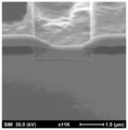
- FIG. It is a figure which shows the cross-sectional photograph of the trench of Example 2.
- the semiconductor device obtained in the present invention it is a figure which shows typically one aspect of the Schottky barrier diode (SBD).
- SBD Schottky barrier diode
- the semiconductor device obtained in the present invention it is a figure which shows typically one aspect of the trench MOS type Schottky barrier diode (SBD).
- SBD trench MOS type Schottky barrier diode
- JBS junction barrier Schottky diode
- MOSFET typically one aspect of MOSFET.
- MOSFET typically one aspect of MOSFET.
- FIG. 1 It is a figure explaining the angle formed by the side surface of a trench and the first surface of a crystalline oxide semiconductor layer in embodiment of the semiconductor device obtained in this invention. It is a figure explaining the taper angle when the side surface of the trench in the embodiment of the semiconductor device obtained in this invention is tapered. It is a figure which shows the cross-sectional photograph of the trench of Example 3. FIG. It is explanatory drawing which shows the structure of the trench of Example 3. FIG.
- the method for etching a crystalline oxide of the present invention includes at least etching a crystalline oxide, and is characterized in that the etching is performed under a pressure of 1 Pa or more and 10 Pa or less with respect to the crystalline oxide. And. Further, the method for forming a trench of a crystalline oxide semiconductor layer of the present invention includes etching the crystalline oxide semiconductor layer to form at least one trench in the crystalline oxide semiconductor layer, and the etching is performed. It is characterized in that it is performed under a pressure of 1 Pa or more and 10 Pa or less with respect to the crystalline oxide semiconductor layer.
- the etching may be dry etching or wet etching, but the etching is made into plasma. It is preferably performed using gas, and more preferably an ICP-RIE apparatus is used. Further, in the present invention, the pressure is preferably 2 Pa or more, and most preferably 5 Pa or more. Further, in the present invention, the etching is preferably performed using at least halogen, and more preferably chlorine. Further, in the present invention, the etching is preferably performed in an atmosphere of an inert gas, more preferably in an Ar atmosphere.
- the etching in a halogen gas atmosphere, and it is more easy to perform the etching in a chlorine gas atmosphere because a trench more suitable for a semiconductor device such as a power device can be formed more easily.
- the plasma bias of the etching gas is 25 W or more.
- the crystalline oxide contains at least gallium.
- the crystalline oxide has a ⁇ -gallia structure or a corundum structure, and even when the crystalline oxide has a metastable phase crystal structure, etching can be performed satisfactorily.
- the crystalline oxide is layered.
- the crystalline oxide is a crystalline oxide semiconductor.
- a crystalline oxide semiconductor layer including at least one trench and at least one electrode electrically connected to the crystalline oxide semiconductor layer are included, and the bottom surface of the trench is included. It has at least one arc portion between the side surface and the side surface, and the radius of curvature of the arc portion is in the range of 100 nm to 500 nm, and forms between the side surface and the first surface of the crystalline oxide semiconductor layer.
- a semiconductor device having an angle of 90 ° or more can be easily obtained.
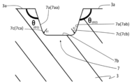
- the "radius of curvature” refers to the radius of the osculating circle with respect to the curve of the arc portion in the trench cross section.
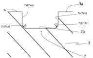
- the "arc portion” may include not only a part of a perfect circle but also a part of an ellipse and have an arc shape as a whole. For example, a part of a shape in which the corners of a polygon are rounded. It may be. That is, the arc portion may be a portion having a curved shape in the cross section of the trench, and may be provided at least in a part between the side surface and the bottom surface. For example, an example of an arc portion is shown in FIG.
- the crystalline oxide semiconductor shown in FIG. 2 includes an arc portion 7c having two radii of curvature.
- both R1 and R2 have a radius of curvature in the range of 100 nm to 500 nm.
- the trench may have an arc portion in the entire space between the bottom surface 7b and the side surface 7a of the trench.
- the radius of curvature R1 of the first arc portion 7 ca between the bottom surface 7b of the trench 7 and the first side surface 7aa, and the bottom surface 7b and the second side surface 7ab of the trench.
- the difference between the second arc portion 7cc and the radius of curvature R2 is preferably in the range of 0 to 200 nm, and more preferably in the range of 0 to 50 nm. In the embodiment of the present invention, it is most preferable that the radius of curvature R1 of the first arc portion 7ca and the radius of curvature R2 of the second arc portion 7cc are equal.
- the "angle formed by the side surface and the first surface of the crystalline oxide semiconductor layer” is the side surface of the trench provided on the first surface 3a side of the crystalline oxide semiconductor layer 3 in the trench 7 cross section.
- the angle formed by 7a and the first surface 3a of the crystalline oxide semiconductor layer 3 is usually about 90 ° or more in the embodiment of the present invention.
- Examples of such an "angle formed by the side surface and the first surface of the crystalline oxide semiconductor layer” include an angle represented by ⁇ ( ⁇ 1, ⁇ 2) in FIGS. 14 and 16-b. ..
- the angle ⁇ 1 formed by the first side surface 7aa of the trench 7 and the first surface 3a of the crystalline oxide semiconductor layer, the second side surface 7ab of the trench 7, and the crystalline oxidation By having the angle ⁇ 2 formed by the first surface 3a of the physical semiconductor layer 3, an excellent electric field relaxation effect can be realized and the on-resistance can be lowered. Further, the upper limit of the above-mentioned "angle formed by the side surface and the first surface of the crystalline oxide semiconductor layer" is not limited as long as the object of the present invention is not impaired, but is preferably 150 °.
- the angle ( ⁇ 1) formed by the first side surface 7aa of the trench 7 and the first surface 3a of the crystalline oxide semiconductor layer and the trench 7 It is preferable that the angle ( ⁇ 2) formed by the second side surface 7ab is equal.
- the trench is formed in the crystalline oxide semiconductor layer, and is not particularly limited as long as the object of the present invention is not impaired.
- the depth of the trench is not particularly limited, but in the present invention, the depth of the trench in the cross section of the trench is usually 200 nm or more, preferably 500 nm or more, and more preferably 1 ⁇ m or more.
- the upper limit of the depth of the trench is not particularly limited, but is preferably 100 ⁇ m, and more preferably 10 ⁇ m.
- the width of the trench in the cross section of the trench is also not particularly limited, but is usually 200 nm or more, preferably 500 nm or more.
- the upper limit of the width of the trench is not particularly limited, but is preferably 100 ⁇ m, and more preferably 10 ⁇ m.
- the trench in such a preferable range, it is possible to exhibit more excellent semiconductor characteristics as a semiconductor device such as a power device.
- a semiconductor device such as a power device.
- the width of the trench is narrowed toward the bottom surface is given as a preferable example, and according to such a preferable example, It is preferable because a good interface can be formed and better electrical characteristics can be obtained.
- the side surface of the trench is tapered and the side surface has a taper angle with respect to the first surface of the crystalline oxide semiconductor layer.
- the taper angle was defined as a virtual surface (taper angle 0 ° because it does not have a taper shape) perpendicular to the first surface of the crystalline oxide semiconductor layer and the first surface in the trench cross section. In some cases, it refers to the angle formed by the virtual surface and the side surface (having a tapered shape) of the trench. Examples of the taper angle include an angle represented by ⁇ ( ⁇ 3, ⁇ 4) in FIG. In the present invention, the taper angle is preferably in the range of more than 0 ° and 45 ° or less. That is, the angle formed by the side surface and the first surface of the crystalline oxide semiconductor layer (for example, ⁇ 1 and ⁇ 2 shown in FIGS.
- the electrode may be a known one, and may be any of, for example, a Schottky electrode, an ohmic electrode, a gate electrode, a drain electrode, a source electrode, and the like.
- the electrode may be a known electrode that is appropriately set depending on the type of the semiconductor device or the like, and examples of the electrode material include D block metal and the like.
- the electrode may be referred to as a barrier electrode, for example.
- the barrier electrode is not particularly limited as long as it forms a Schottky barrier having a predetermined barrier height at the interface with the semiconductor region.
- the electrode material of the barrier electrode is not particularly limited as long as it can be used as a barrier electrode, and may be a conductive inorganic material or a conductive organic material.
- the electrode material is preferably metal.
- the metal is not particularly limited, but preferably, for example, at least one metal selected from the 4th to 11th groups of the periodic table can be mentioned.
- the metal of Group 4 of the periodic table include titanium (Ti), zirconium (Zr), hafnium (Hf), and the like, and Ti is preferable.
- the metal of Group 5 of the periodic table include vanadium (V), niobium (Nb), and tantalum (Ta).
- Examples of the metal of Group 6 of the periodic table include one or more metals selected from chromium (Cr), molybdenum (Mo), tungsten (W) and the like. Cr is preferable because the semiconductor characteristics such as switching characteristics become better.
- Examples of the metal of Group 7 of the periodic table include manganese (Mn), technetium (Tc), and rhenium (Re).
- Examples of the metal of Group 8 of the periodic table include iron (Fe), ruthenium (Ru), and osmium (Os).
- Examples of the metal of Group 9 of the periodic table include cobalt (Co), rhodium (Rh), and iridium (Ir).
- Examples of the metal of Group 10 of the periodic table include nickel (Ni), palladium (Pd), platinum (Pt), and the like, and Pt is preferable.
- Examples of the metal of Group 11 of the periodic table include copper (Cu), silver (Ag), and gold (Au).
- Examples of the means for forming the barrier electrode include known means, and more specifically, examples include a dry method and a wet method.
- Examples of the dry method include known means such as sputtering, vacuum deposition, and CVD.
- Examples of the wet method include screen printing and die coating.
- the crystalline oxide semiconductor layer is not particularly limited as long as it forms a semiconductor region in the semiconductor device.
- the crystalline oxide semiconductor layer (hereinafter, also simply referred to as “semiconductor region”) is not particularly limited as long as it contains a semiconductor as a main component, but in the present invention, the semiconductor region is a crystalline oxide semiconductor. Is preferably contained as a main component, and more preferably an n-type semiconductor region containing an n-type semiconductor as a main component.
- the crystalline oxide semiconductor preferably has a ⁇ -gaul structure or a corundum structure, and more preferably has a corundum structure.
- the semiconductor region preferably contains at least gallium, more preferably contains a gallium compound as a main component, more preferably contains an InAlGaO-based semiconductor as a main component, and ⁇ -Ga 2 O 3 or a mixed crystal thereof. Is most preferable to be contained as a main component.
- the "main component" is, for example, when the crystalline oxide semiconductor is ⁇ -Ga 2 O 3 , the atomic ratio of gallium in the metal element in the semiconductor region is 0.5 or more, and ⁇ -Ga. It is sufficient if 2 O 3 is included.
- the atomic ratio of gallium in the metal element in the semiconductor region is preferably 0.7 or more, more preferably 0.8 or more.
- the semiconductor region is usually a single-phase region, but may have a second semiconductor region or another phase composed of a different semiconductor phase as long as the object of the present invention is not impaired.
- the semiconductor region is usually in the form of a film, and may be a semiconductor film.
- the thickness of the semiconductor film in the semiconductor region is not particularly limited and may be 1 ⁇ m or less or 1 ⁇ m or more, but in the present invention, it is preferably 1 ⁇ m to 40 ⁇ m, and 1 ⁇ m to 1 ⁇ m. It is more preferably 25 ⁇ m.
- the withstand voltage of the crystalline oxide semiconductor layer is increased by, for example, making it a thick film or lowering the carrier concentration.
- the gallium oxide-based crystalline oxide semiconductor layer containing ⁇ -Ga 2 O 3 and ⁇ -Ga 2 O 3 has an arc portion having a radius of curvature in the range of 100 nm to 500 nm.
- the electric field relaxation effect is obtained by having a trench including the trench and having an angle formed by the side surface of the trench and the first surface of the crystalline oxide semiconductor layer within a range of more than 90 ° and not more than 135 °. Sufficiently obtained.
- the thickness of the gallium oxide-based crystalline oxide semiconductor layer (including the drift region) is reduced (for example, 10 ⁇ m or less). Even with such a thickness, a semiconductor device having a high withstand voltage (for example, 3000 V or more) can be realized. Further, according to the embodiment of the present invention, the thickness of the gallium oxide-based crystalline oxide semiconductor layer (including the drift region) can be further reduced (for example, 2.0 ⁇ m or less). Even with a thickness, a semiconductor device having a high withstand voltage (for example, 600 V or more) can be realized.
- the carrier concentration of the gallium oxide-based crystalline oxide semiconductor layer can be 5.0 ⁇ 10 16 / cm 3 or more, which is preferable. , 3.0 ⁇ 10 17 / cm 3 or more.
- the thickness of the crystalline oxide layer and the carrier concentration are appropriately adjusted according to the required pressure resistance, but in the embodiment of the present invention, as described above, even if the thickness is thinner or the carrier concentration is higher than before, the pressure resistance is high. As a result, the on-resistance can be lowered.
- the surface area of the semiconductor film is not particularly limited, and may be 1 mm 2 or more, may be 1 mm 2 or less.
- the crystalline oxide semiconductor is usually a single crystal, but may be a polycrystal. Further, the semiconductor film may be a single-layer film or a multilayer film. When the semiconductor film is a multilayer film, the multilayer film preferably has a thickness of 40 ⁇ m or less, and is a multilayer film including at least a first semiconductor layer and a second semiconductor layer. When the Schottky electrode is provided on the first semiconductor layer, it is also preferable that the carrier concentration of the first semiconductor layer is smaller than the carrier concentration of the second semiconductor layer.
- the second semiconductor layer usually contains a dopant, and the carrier concentration of the semiconductor layer (including the first semiconductor layer and the second semiconductor layer) adjusts the doping amount. By doing so, it can be set as appropriate.
- the semiconductor film preferably contains a dopant.
- the dopant is not particularly limited and may be a known one. Examples of the dopant include n-type dopants such as tin, germanium, silicon, titanium, zirconium, vanadium and niobium, and p-type dopants. In the present invention, the dopant is preferably Sn, Ge or Si.
- the content of the dopant is preferably 0.00001 atomic% or more, more preferably 0.00001 atomic% to 20 atomic%, and 0.00001 atomic% to 10 atomic% in the composition of the semiconductor film. Is most preferable.
- the dopant used for the first semiconductor layer is germanium, silicon, titanium, zirconium, vanadium or niobium
- the dopant used for the second semiconductor layer is tin, which provides adhesion. It is preferable because the semiconductor characteristics are further improved without impairing.
- the semiconductor film is formed by, for example, a means such as a mist CVD method, and more specifically, for example, the raw material solution is atomized (atomization step), and the obtained atomized droplets (including mist) are carried.
- a semiconductor film containing a crystalline oxide semiconductor as a main component is laminated on the substrate by transporting the atomized droplets to the substrate with gas (transportation step) and then thermally reacting the atomized droplets in the film forming chamber (conveying step). It is suitably formed by the film forming step).
- the raw material solution is atomized, the atomized droplets are suspended, and atomized droplets are generated.
- the method for atomizing the raw material solution is not particularly limited as long as the raw material solution can be atomized, and may be a known means, but in the present invention, the atomization method using ultrasonic waves is preferable.
- Atomized droplets obtained using ultrasonic waves have a zero initial velocity and are preferable because they float in the air. For example, instead of spraying them like a spray, they float in space and are transported as gas. Since it is possible, it is not damaged by collision energy, so it is very suitable.
- the droplet size is not particularly limited and may be a droplet of about several mm, but is preferably 50 ⁇ m or less, and more preferably 100 nm to 10 ⁇ m.
- the raw material solution is not particularly limited as long as it contains a raw material capable of atomizing and forming a semiconductor region, and may be an inorganic material or an organic material, but in the present invention, it may be an inorganic material or an organic material.
- the raw material is preferably a metal or a metal compound, and is selected from gallium, iron, indium, aluminum, vanadium, titanium, chromium, rhodium, nickel, cobalt, zinc, magnesium, calcium, silicon, yttrium, strontium and barium. More preferably, it contains one or more metals.
- a solution in which the metal is dissolved or dispersed in an organic solvent or water in the form of a complex or a salt can be preferably used.
- the form of the complex include an acetylacetonate complex, a carbonyl complex, an ammine complex, and a hydride complex.
- the salt form include organic metal salts (for example, metal acetate, metal oxalate, metal citrate, etc.), metal sulfide salts, nitrified metal salts, phosphor oxide metal salts, and metal halide metal salts (for example, metal chloride). Salts, metal bromide salts, metal iodide salts, etc.) and the like.
- an additive such as a hydrohalic acid or an oxidizing agent with the raw material solution.
- the hydrohalic acid include hydrobromic acid, hydrochloric acid, and hydroiodic acid. Among them, hydrobromic acid or hydroiodic acid because a better quality film can be obtained. Is preferable.
- the oxidizing agent include hydrogen peroxide (H 2 O 2 ), sodium peroxide (Na 2 O 2 ), barium peroxide (BaO 2 ), benzoyl peroxide (C 6 H 5 CO) 2 O 2 and the like. Examples include hydrogen peroxide, hypochlorous acid (HClO), perchloric acid, nitric acid, ozone water, and organic peroxides such as peracetic acid and nitrobenzene.
- the raw material solution may contain a dopant. Doping can be performed satisfactorily by including the dopant in the raw material solution.
- the dopant is not particularly limited as long as it does not interfere with the object of the present invention.
- Examples of the dopant include n-type dopants such as tin, germanium, silicon, titanium, zirconium, vanadium and niobium, and p-type dopants.
- the concentration of the dopant may usually be about 1 ⁇ 10 16 / cm 3 to 1 ⁇ 10 22 / cm 3 , and the concentration of the dopant should be as low as about 1 ⁇ 10 17 / cm 3 or less, for example. You may.
- the dopant may be contained in a high concentration of about 1 ⁇ 10 20 / cm 3 or more. In the embodiment of the present invention, it is preferably contained at a carrier concentration of 1 ⁇ 10 17 / cm 3 or more. Further, as one of the embodiments of the present invention, in a semiconductor device having a withstand voltage of 600 V, the carrier concentration of the gallium oxide-based crystalline oxide semiconductor layer is 1 ⁇ 10 17 / cm 3 or more and 3 ⁇ 10 17 / cm 3 It can be as follows.
- the solvent of the raw material solution is not particularly limited, and may be an inorganic solvent such as water, an organic solvent such as alcohol, or a mixed solvent of an inorganic solvent and an organic solvent.
- the solvent preferably contains water, and more preferably water or a mixed solvent of water and alcohol.
- the atomized droplets are transported into the film forming chamber by using a carrier gas.
- the carrier gas is not particularly limited as long as the object of the present invention is not impaired, and for example, an inert gas such as oxygen, ozone, nitrogen or argon, or a reducing gas such as hydrogen gas or forming gas is a suitable example. Can be mentioned.
- the type of the carrier gas may be one type, but may be two or more types, and a diluted gas having a reduced flow rate (for example, a 10-fold diluted gas) or the like is further used as the second carrier gas. May be good.
- the carrier gas may be supplied not only at one location but also at two or more locations.
- the flow rate of the carrier gas is not particularly limited, but is preferably 0.01 to 20 L / min, and more preferably 1 to 10 L / min.
- the flow rate of the diluting gas is preferably 0.001 to 2 L / min, more preferably 0.1 to 1 L / min.
- the semiconductor film is formed on the substrate by thermally reacting the atomized droplets in the film forming chamber.
- the thermal reaction may be such that the atomized droplets react with heat, and the reaction conditions and the like are not particularly limited as long as the object of the present invention is not impaired.
- the thermal reaction is usually carried out at a temperature equal to or higher than the evaporation temperature of the solvent, but is preferably not too high (for example, 1000 ° C.) or lower, more preferably 650 ° C. or lower, and most preferably 300 ° C. to 650 ° C. preferable.
- the thermal reaction may be carried out in any of vacuum, non-oxygen atmosphere, reducing gas atmosphere and oxygen atmosphere as long as the object of the present invention is not impaired, but the thermal reaction may be carried out in a non-oxygen atmosphere or oxygen. It is preferably performed in an atmosphere. Further, it may be carried out under any conditions of atmospheric pressure, pressurization and depressurization, but in the present invention, it is preferably carried out under atmospheric pressure.
- the film thickness can be set by adjusting the film formation time.
- the substrate is not particularly limited as long as it can support the semiconductor film.
- the material of the substrate is not particularly limited as long as it does not impair the object of the present invention, and may be a known substrate, an organic compound, or an inorganic compound.
- the shape of the substrate may be any shape and is effective for any shape, for example, plate-like, fibrous, rod-like, columnar, prismatic, such as a flat plate or a disk. Cylindrical, spiral, spherical, ring-shaped and the like can be mentioned, but in the embodiment of the present invention, a substrate is preferable.
- the thickness of the substrate is not particularly limited in the present invention.
- the substrate is not particularly limited as long as it has a plate shape and serves as a support for the semiconductor film. It may be an insulator substrate, a semiconductor substrate, a metal substrate or a conductive substrate, but the substrate is preferably an insulator substrate, and the surface is made of metal. A substrate having a film is also preferable.
- the substrate includes, for example, a base substrate containing a substrate material having a corundum structure as a main component, a substrate substrate containing a substrate material having a ⁇ -gaul structure as a main component, and a substrate material having a hexagonal structure as a main component. Examples include a base substrate.
- the “main component” means that the substrate material having the specific crystal structure is preferably 50% or more, more preferably 70% or more, still more preferably 90% or more, in terms of atomic ratio, with respect to all the components of the substrate material. It means that it is contained in% or more, and may be 100%.
- the substrate material is not particularly limited and may be a known one as long as the object of the present invention is not impaired.
- Examples of the substrate material having the corundum structure are ⁇ -Al 2 O 3 (sapphire substrate) or ⁇ -Ga 2 O 3 , and a-plane sapphire substrate, m-plane sapphire substrate, and r-plane sapphire substrate are preferable.
- C-plane sapphire substrate, ⁇ -type gallium oxide substrate (a-plane, m-plane or r-plane) and the like are more preferable examples.
- the base substrate containing the substrate material having a ⁇ -gaul structure as a main component for example, ⁇ -Ga 2 O 3 substrate or Ga 2 O 3 and Al 2 O 3 are included, and Al 2 O 3 is more than 0 wt%.
- Examples thereof include a mixed crystal substrate having a content of 60 wt% or less.
- Examples of the base substrate containing a substrate material having a hexagonal structure as a main component include a SiC substrate, a ZnO substrate, and a GaN substrate.
- an annealing treatment may be performed after the film forming step.
- the annealing treatment temperature is not particularly limited as long as the object of the present invention is not impaired, and is usually 300 ° C. to 650 ° C., preferably 350 ° C. to 550 ° C.
- the annealing treatment time is usually 1 minute to 48 hours, preferably 10 minutes to 24 hours, and more preferably 30 minutes to 12 hours.
- the annealing treatment may be carried out in any atmosphere as long as the object of the present invention is not impaired, but it is preferably in a non-oxygen atmosphere, and more preferably in a nitrogen atmosphere.
- the semiconductor film may be provided directly on the substrate, or the semiconductor film may be provided via another layer such as a buffer layer (buffer layer) or a stress relaxation layer. You may.
- the means for forming each layer is not particularly limited and may be a known means, but in the embodiment of the present invention, the mist CVD method is preferable.
- the crystalline oxide semiconductor layer contains at least gallium. Further, as one of the preferred embodiments, it is preferable that the crystalline oxide semiconductor layer has a corundum structure.
- the semiconductor film may be used in a semiconductor device as the semiconductor region after using a known means such as peeling from the substrate or the like, or may be used as it is in the semiconductor device as the semiconductor region. You may use it. Further, as one of the preferred embodiments, it is preferable that the crystalline oxide semiconductor layer contains two or more of the trenches.
- the width of the trench is preferably 2 ⁇ m or less, and it is more preferable that the crystalline oxide semiconductor layer contains 4 or more of the trenches.
- the plurality of trenches are arranged on the first surface side of the crystalline oxide semiconductor at intervals from each other.
- the semiconductor device is more suitable as a power device, and more excellent semiconductor characteristics can be obtained.
- it will be more effective for miniaturization of semiconductor devices.
- the crystalline oxide semiconductor layer has at least one arc portion between the bottom surface and the side surface of the trench, and the radius of curvature of the arc portion is in the range of 100 nm to 500 nm.
- the radius of curvature of at least one arc portion is within the range of 100 nm to 500 nm.
- the radius of curvature of the two or more arc portions is preferably in the range of 100 nm to 500 nm, and all arcs. It is more preferable that the radius of curvature of the portion is in the range of 100 nm to 500 nm.
- At least one trench 7 is provided on the first surface 3a side of the crystalline oxide semiconductor layer 3 (also referred to as a semiconductor region).
- the trench 7 includes a bottom surface, a side surface, and at least one arc portion between the bottom surface and the side surface.
- the crystalline oxide semiconductor layer 3 is electrically connected to the electrode.
- FIG. 1 shows a junction barrier Schottky diode (JBS) as a semiconductor device which is one of the embodiments of the present invention.
- JBS junction barrier Schottky diode
- the barrier height adjusting region 1 includes a barrier electrode 2 provided on the semiconductor region 3 and capable of forming a Schottky barrier between the semiconductor region 3, and the barrier electrode 2 and the semiconductor region 3. It includes a barrier height region provided between the semiconductor regions 3 and capable of forming a Schottky barrier having a barrier height larger than that of the Schottky barrier of the barrier electrode 2.
- the barrier height adjusting region 1 is embedded in a trench 7 provided on the first surface 3a side of the semiconductor region 3. In the embodiment of the present invention, it is preferable that a plurality of trenches 7 and a plurality of barrier height adjusting regions 1 arranged in the plurality of trenches 7 are provided at regular intervals, and both ends of the barrier electrode and the semiconductor region are provided.
- the barrier height adjusting regions are provided between the two.
- the JBS is configured so as to be excellent in thermal stability and adhesion, the leakage current is further reduced, and the semiconductor characteristics such as withstand voltage are further excellent.
- the semiconductor device of FIG. 1 includes an ohmic electrode 4 on the second surface 3b side of the semiconductor region 3.
- the semiconductor device of FIG. 1 has an arc portion 7c between the bottom surface 7a and the side surface 7b of the trench 7, and the radius of curvature of the arc portion is in the range of 100 nm to 500 nm, and the electric field relaxation effect is excellent. As a result, the on-resistance can be lowered.
- each layer of the semiconductor device of FIG. 1 is not particularly limited as long as the object of the present invention is not impaired, and may be known means. Examples thereof include a means of forming a film by a vacuum vapor deposition method, a CVD method, a sputtering method, various coating techniques, and the like, and then patterning by a photolithography method, or a means of directly patterning by using a printing technique or the like.
- FIG. 9 shows an example of a Schottky barrier diode (SBD) according to an embodiment of the present invention.
- the SBD of FIG. 9 includes an n-type semiconductor layer 101a, an n + type semiconductor layer 101b, a dielectric layer 104, a Schottky electrode 105a, and an ohmic electrode 105b. Further, the SBD of FIG. 9 has a trench structure including the arc portion, and the p-type semiconductor layer 102 is embedded in the trench 7.
- the material of the Schottky electrode and the ohmic electrode may be a known electrode material, and the electrode material includes, for example, Al, Mo, Co, Zr, Sn, Nb, Fe, Cr, Ta, Ti, Au, etc.
- Metals such as Pt, V, Mn, Ni, Cu, Hf, W, Ir, Zn, In, Pd, Nd or Ag or alloys thereof, tin oxide, zinc oxide, indium oxide, indium tin oxide (ITO), oxidation Examples thereof include metal oxide conductive films such as indium tin oxide (IZO), organic conductive compounds such as polyaniline, polythiophene or polypyrrole, or mixtures thereof.
- the Schottky electrode and the ohmic electrode can be formed by a known means such as a vacuum deposition method or a sputtering method. More specifically, for example, when forming a Schottky electrode, a layer made of Mo and a layer made of Al are laminated, and the layer made of Mo and the layer made of Al are patterned using a photolithography technique. It can be done by.
- the depletion layer (not shown) is contained in the n-type semiconductor layer 101a as the crystalline oxide semiconductor layer due to the stress relaxation action of the arc portion of the trench 7. Since it spreads well, it becomes a high withstand voltage SBD. Further, when a forward bias is applied, the position is located on the first surface side of the crystalline oxide semiconductor layer from the ohmic electrode 105b located on the second surface side opposite to the first surface side of the crystalline oxide semiconductor layer. Electrons flow to the Schottky electrode 105a.
- the SBD using the semiconductor structure in this way is excellent for high withstand voltage and large current, has a high switching speed, and is also excellent in withstand voltage and reliability.
- Examples of the material of the dielectric layer 104 include GaO, AlGaO, InAlGaO, AlInZnGaO 4 , AlN, Hf 2 O 3 , SiN, SiON, Al 2 O 3 , MgO, GdO, SiO 2 or Si 3 N 4. Be done. By using such an insulator for the insulator layer, the function of the semiconductor property at the interface can be satisfactorily exhibited.
- the dielectric layer 104 is provided between the n-type semiconductor layer 101 and the Schottky electrode 105a.
- the insulator layer can be formed by a known means such as a sputtering method, a vacuum vapor deposition method, or a CVD method.
- FIG. 10 shows an n-type semiconductor layer 101a as a crystalline oxide semiconductor layer, which has two or more trenches 7 arranged on the first surface side of the n-type semiconductor layer 101a.
- An example of an embodiment of a trench type Schottky barrier diode (SBD) including a semiconductor layer 101a, an n + type semiconductor layer 101b, a dielectric layer 104, a Schottky electrode 105a, and an ohmic electrode 105b is shown.
- the trench-type SBD of FIG. 10 has a trench structure including the arc portion. According to such a trench type SBD, the leakage current can be significantly reduced while maintaining a higher withstand voltage, and as a result, a significantly lower on-resistance can be achieved.
- FIG. 11 shows the implementation of a junction barrier Schottky diode (JBS) including an n-type semiconductor layer 101a, an n + type semiconductor layer 101b, a p-type semiconductor layer 102, a dielectric layer 104, a Schottky electrode 105a, and an ohmic electrode 105b.
- JBS junction barrier Schottky diode
- the JBS of FIG. 11 has a trench 7 having the arc portion, and the p-type semiconductor layer 102 is embedded in the trench structure. According to such a JBS, the leakage current can be significantly reduced while maintaining a higher withstand voltage than the trench type SBD of FIG. 10, and as a result, a significantly lower on-resistance can be achieved. It will be possible.
- FIG. 12 shows an example of an embodiment when the semiconductor device is a MOSFET.
- the MOSFET in FIG. 12 is a trench-type MOSFET, which is an n-type semiconductor layer 131a as a crystalline oxide semiconductor layer, and the n-type semiconductor layer 131a, the n + -type semiconductor layers 131b, and 131c including the trench 7. , A gate insulating film 134, and a gate electrode 135a, a source electrode 135b, and a drain electrode 135c.
- n + type semiconductor layer 131b having a thickness of, for example, 100 nm to 100 ⁇ m is formed on the drain electrode 135c, and an n-type semiconductor layer 131a having a thickness of, for example, 100 nm to 100 ⁇ m is formed on the n + type semiconductor layer 131b.
- an n + type semiconductor layer 131c is formed on the n ⁇ type semiconductor layer 131a, and a source electrode 135b is formed on the n + type semiconductor layer 131c.
- grooves are formed as a plurality of trenches 7 having a depth that penetrates the n + semiconductor layer 131c and reaches halfway through the n-type semiconductor layer 131a. It is formed.
- Each of such trenches 7 is provided with the arc portion between the bottom surface and the side surface of the trench 7.
- a gate electrode 135a is embedded in the trench 7 via, for example, a gate insulating film 134 having a thickness of 10 nm to 1 ⁇ m.
- the n ⁇ type is applied.
- a channel layer is formed on the side surface of the semiconductor layer 131a, and electrons are injected into the n-type semiconductor layer to turn on.
- the off state by setting the voltage of the gate electrode to 0V, the channel layer cannot be formed, the n-type semiconductor layer is filled with the depletion layer, and the turn-off occurs.
- a known means can be appropriately used for manufacturing the MOSFET of FIG. 12.
- an etching mask is provided in a predetermined region of the n-type semiconductor layer 131a and the n + type semiconductor layer 131c, and etching is performed by the above-mentioned preferable high-pressure dry etching method to perform the etching from the surface of the n-type semiconductor layer 131c to the n-type semiconductor layer.
- a groove of the trench 7 having a depth reaching the middle of 131a is formed together with the arc portion.
- a gate insulating film 134 having a thickness of, for example, 50 nm to 1 ⁇ m is formed on the side surface and the bottom surface of the groove of the trench 7 by using known means such as a thermal oxidation method, a vacuum vapor deposition method, a sputtering method, and a CVD method.
- a gate electrode material such as polysilicon is formed in the groove of the trench 7 at a thickness equal to or less than the thickness of the n-type semiconductor layer by using a CVD method, a vacuum vapor deposition method, a sputtering method, or the like.
- the source electrode 135b is formed on the n + type semiconductor layer 131c and the drain electrode 135c is formed on the n + type semiconductor layer 131b by using known means such as a vacuum deposition method, a sputtering method, and a CVD method.
- Power MOSFETs can be manufactured.
- the electrode materials of the source electrode and the drain electrode may be known electrode materials, respectively, and the electrode materials include, for example, Al, Mo, Co, Zr, Sn, Nb, Fe, Cr, Ta, and Ti.
- FIG. 12 shows an example of a trench-type vertical MOSFET
- the present invention is not limited to this, and can be applied to various forms of a trench-type MOSFET.
- the depth of the groove of the trench 7 in FIG. 12 may be dug down to a depth reaching the bottom surface of the n-type semiconductor layer 131a to reduce the series resistance.
- FIG. 12 shows an example of another trench-type MOSFET is shown in FIG.
- FIG. 13 shows an n ⁇ type semiconductor layer 131a, a first n + type semiconductor layer 131b, a second n + type semiconductor layer 131c, a p-type semiconductor layer 132, a p + type semiconductor layer 132a, a gate insulating film 134, and a gate electrode 135a.
- An example of an embodiment of a metal oxide semiconductor field effect transistor (MOSFET) including a source electrode 135b and a drain electrode 135c is shown.
- the p + type semiconductor layer 132a may be a p-type semiconductor layer or may be the same as the p-type semiconductor layer 132.
- the semiconductor device is particularly preferably a power device. Further, as one of the embodiments, it is preferable that the semiconductor device is a vertical device. Examples of the semiconductor device include a diode or a transistor (for example, MESFET), and among them, a diode is preferable, and a junction barrier Schottky diode (JBS) is more preferable.
- a diode or a transistor for example, MESFET
- JBS junction barrier Schottky diode
- the semiconductor device is preferably used as a power module, an inverter or a converter by using known means, and further preferably used for a semiconductor system using, for example, a power supply device.
- the power supply device can be manufactured from the semiconductor device or as the semiconductor device by connecting to a wiring pattern or the like by using a known means.
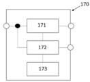
- the power supply system 170 is configured by using the plurality of power supply devices 171 and 172 and the control circuit 173.
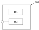
- the power supply system can be used in the system apparatus 180 by combining the electronic circuit 181 and the power supply system 182.
- An example of the power supply circuit diagram of the power supply device is shown in FIG. FIG.
- FIG. 5 shows a power supply circuit of a power supply device including a power circuit and a control circuit.
- the DC voltage is switched at a high frequency by an inverter 192 (composed of MOSFETs A to D), converted to AC, and then insulated and transformed by a transformer 193.
- an inverter 192 composed of MOSFETs A to D
- DCL195 smoothing coils L1 and L2
- a capacitor smoothing coils L1 and L2
- a DC voltage is output.
- the voltage comparator 197 compares the output voltage with the reference voltage
- the PWM control circuit 196 controls the inverter 192 and the rectifier MOSFET 194 so as to obtain a desired output voltage.
- Example 1 Formation of semiconductor layer 1-1.
- Film formation device The mist CVD device 19 used in the examples will be described with reference to FIG.
- the film forming apparatus 19 of FIG. 6 supplies a carrier gas source 22a for supplying a carrier gas, a flow control valve 23a for adjusting the flow rate of the carrier gas sent out from the carrier gas source 22a, and a carrier gas (diluted).
- Preparation for film formation 1-2 The raw material solution 24a obtained in 1) was housed in the mist generation source 24. Next, as the substrate 20, a sapphire substrate was placed on the susceptor 21, and the heater 28 was operated to raise the temperature inside the film forming chamber 30 to 630 ° C. Next, the flow rate control valves 23a and 23b are opened, carrier gas is supplied into the film forming chamber 30 from the carrier gas supply means 22a and 22b which are carrier gas sources, and the atmosphere of the film forming chamber 30 is sufficiently filled with the carrier gas. After the replacement, the flow rate of the carrier gas was adjusted to 1 L / min, and the flow rate of the carrier gas (dilution) was adjusted to 2 L / min. Nitrogen was used as the carrier gas.
- the ultrasonic transducer 26 was vibrated at 2.4 MHz, and the vibration was propagated to the raw material solution 24a through water 25a to atomize the raw material solution 24a to generate mist.
- This mist was introduced into the film forming chamber 30 by the carrier gas, and the mist reacted in the film forming chamber 30 at 630 ° C. under atmospheric pressure to form a semiconductor film on the substrate 20.
- the film thickness was 4.1 ⁇ m, and the film formation time was 105 minutes.
- Etching A trench was formed in the semiconductor film using an ICP-RIE apparatus under the conditions shown in Table 1 below.
- Each of the trenches of the examples had an arc portion, and the radius of curvature of the arc portion was in the range of 100 nm or more and 500 nm or less.
- a cross-sectional photograph of the trench formed as Example 1 is shown in FIG.
- the radius of curvature of Example 1 was 140 nm for R1 (left side) and 160 nm for R2 (right side).
- the side surface of the trench had a taper angle, and the taper angle was 60 °.
- a good trench was formed. Further, the tendency for such a good trench to be formed was observed in the pressure range of 1 Pa to 10 Pa, particularly 2 Pa to 10 Pa, other than the pressure of 5 Pa.
- Example 2 A trench was formed in the same manner as in Example 1 except that the etching was performed under the conditions shown in Table 1.
- a cross-sectional photograph of the obtained trench is shown in FIG.
- the radius of curvature of the arc portion of the trench was 125 nm for R1 (left side) and 298 nm for R2 (right side).
- a trench having a good quality arc portion was formed.
- Example 3 A trench was formed in the semiconductor film (also referred to as a crystalline oxide semiconductor layer) in the same manner as in Example 1 except that the etching was performed under the conditions shown in Table 2.
- a cross-sectional photograph of the obtained trench is shown in FIG. 16-a. Further, FIG. 16-b shows an explanatory view using the same cross-sectional photograph.
- the radius of curvature R1 (left side) of the first arc portion 7ca of the trench 7 was 220 nm
- the radius of curvature R2 (right side) of the second arc portion 7cc was also 220 nm.
- a plurality of trenches 7 were formed in the crystalline oxide semiconductor layer 3, and in each of the trenches 7, trenches 7 having the same radius of curvature of the first arc portion 7ca and the second arc portion 7cc were formed.
- the width of the trench 7 narrows toward the bottom surface.
- the angle ( ⁇ 1 shown in FIG. 16-b) formed by the side surface 7a (first side surface 7aa) of the trench and the first surface 3a of the crystalline oxide semiconductor layer 3 exceeds 90 °.
- the angle between the side surface 7a (second side surface 7ab) of the trench and the first surface 3a of the crystalline oxide semiconductor layer 3 ( ⁇ 2 shown in FIG. 16-b) is within the range of 135 ° or less.
- SiO 2 shown in FIG. 16-b is a mask, which is provided on the crystalline oxide semiconductor layer 3 in order to perform etching to form a trench, and is finally removed. Further, when the crystalline oxide semiconductor layer was obtained by changing the flow rate of BCl 3 , it was found that a trench having a better arc portion could be obtained by setting the crystal oxide semiconductor layer in the range of 50 sccm to 100 sccm.
- the trench cross section has a trench including an arc portion having a radius of curvature in the range of 100 nm to 500 nm, and the side surface of the trench and the crystalline oxide.
- the angle formed by the first surface of the semiconductor layer exceeds 90 ° and is within the range of 135 ° or less, the electric field relaxation effect can be sufficiently obtained. As a result, it has become possible to reduce the on-resistance of the semiconductor device having the gallium oxide-based crystalline oxide semiconductor layer.
- the on-resistance of the semiconductor device can be further reduced. Can be expected.
- Example 1 A trench was formed in the same manner as in Example 1 except that etching was performed under the conditions shown in Table 1.
- the obtained trench had a convex bottom surface and had corners between the bottom surface and the side surface, so that a poor quality trench was formed.
- Example 2 A trench was formed in the same manner as in Example 1 except that etching was performed under the conditions shown in Table 1.
- the side surface of the obtained trench was hollowed out in an inverted tapered shape, and the width inside the trench was wider than the opening of the trench. Further, although an arc portion was formed between the bottom surface and the side surface, the arc portion protruded greatly and the radius of curvature was 1 ⁇ m or more, and a trench of poor quality was formed.
- the method of the present invention can be used in all fields such as semiconductors (for example, compound semiconductor electronic devices, etc.), electronic parts / electrical equipment parts, optical / electrophotographic related devices, industrial parts, etc., but is particularly useful for manufacturing power devices. Is.
Landscapes
- Engineering & Computer Science (AREA)
- Microelectronics & Electronic Packaging (AREA)
- Power Engineering (AREA)
- Physics & Mathematics (AREA)
- Condensed Matter Physics & Semiconductors (AREA)
- General Physics & Mathematics (AREA)
- Computer Hardware Design (AREA)
- Ceramic Engineering (AREA)
- Manufacturing & Machinery (AREA)
- Plasma & Fusion (AREA)
- Electrodes Of Semiconductors (AREA)
Abstract
結晶性酸化物に対して1Pa以上10Pa以下の圧力下にて結晶性酸化物をエッチングして、底面と側面との間に、曲率半径が100nm~500nmの範囲内である少なくとも1つの円弧部を有しているトレンチを形成する。
Description
本発明は、結晶性酸化物のエッチング方法に関する。また、本発明は、結晶性酸化物半導体層のトレンチ形成方法に関する。さらに、本発明はトレンチ形成方法を含む半導体装置の製造方法に関する。
次世代半導体材料として酸化ガリウムが注目を集めている。酸化ガリウムはバンドギャップが大きく高耐圧大電流半導体デバイスを実現することができる材料として期待されており、逆方向耐圧を大きくし、さらに順方向立ち上がり電圧を小さくすること等を目的に、種々検討されている。
近年においては、トレンチを有する半導体デバイスが検討されている。β―Ga2O3のトレンチ型半導体デバイスとして、例えば、特許文献1~3に記載の半導体デバイスが開示されている。また、α―Ga2O3のトレンチ型半導体デバイスとして、例えば、特許文献4および5に記載の半導体デバイスが開示されている。
しかしながら、酸化ガリウムなどの結晶性酸化物半導体にトレンチを形成した場合、他の半導体材料とは異なるエッチング特性を有するため、トレンチ底面において電界緩和が期待できる曲率半径が100nm以上の円弧部を形成することが困難であった。例えば、従来のドライエッチングの条件にて結晶性酸化ガリウムを無理にエッチングした場合、トレンチ底面にでこぼこが出来てしまったり、トレンチの開口部よりもトレンチ内部の幅が広くなってしまったりして電界緩和効果が十分に発揮されず、例えばオン抵抗が上がってしまうなどの問題があった。
本発明は、優れた半導体特性を有するトレンチを工業的有利に形成できる方法を提供することを目的とする。
本発明者らは、上記目的を達成すべく鋭意検討した結果、特定の高圧ドライエッチングを用いて結晶性酸化物半導体層にトレンチを形成することにより、少なくとも1つのトレンチを含む結晶性酸化物半導体層と、前記結晶性酸化物半導体層と電気的に接続されている少なくとも1つの電極とを含み、前記トレンチの底面と側面との間に少なくとも1つの円弧部を有しており、前記円弧部の曲率半径が100nm~500nmの範囲内であり、前記側面と前記結晶性酸化物半導体層の第1面とのなす角が90°以上である半導体装置の創製に成功し、このようなエッチング方法が、上記した従来の問題を一挙に解決できるものであることを見出した。
また、本発明者らは、上記知見を得た後、さらに検討を重ねて本発明を完成させるに至った。
また、本発明者らは、上記知見を得た後、さらに検討を重ねて本発明を完成させるに至った。
[1] 結晶性酸化物をエッチングすることを少なくとも含み、前記のエッチングを、前記結晶性酸化物に対して1Pa以上10Pa以下の圧力下にて行う、結晶性酸化物のエッチング方法。
[2] 前記エッチングを、プラズマ化したエッチングガスを用いて行う前記[1]記載のエッチング方法。
[3] 前記圧力が2Pa以上である、前記[1]または[2]に記載のエッチング方法。
[4] 前記エッチングを、少なくともハロゲンを用いて行う、前記[1]~[3]のいずれかに記載のエッチング方法。
[5] 前記エッチングを不活性ガスの雰囲気下で行う前記[1]~[4]のいずれかに記載のエッチング方法。
[6] 前記エッチングをハロゲンガスの雰囲気下で行う前記[1]~[4]のいずれかに記載のエッチング方法。
[7] 前記エッチングガスのプラズマのバイアスが25W以上である前記[2]記載のエッチング方法。
[8] 前記結晶性酸化物が少なくともガリウムを含む前記[1]~[7]のいずれかに記載のエッチング方法。
[9] 前記結晶性酸化物がコランダム構造を有する前記[1]~[8]のいずれかに記載のエッチング方法。
[10] 前記結晶性酸化物が層状である前記[1]~[9]のいずれかに記載のエッチング方法。
[11] 前記結晶性酸化物が結晶性酸化物半導体である前記[1]~[10]のいずれかに記載のエッチング方法。
[12] 結晶性酸化物半導体層をエッチングして前記結晶性酸化物半導体層に少なくとも1つのトレンチを形成することを含み、前記のエッチングを、前記結晶性酸化物半導体層に対して1Pa以上10Pa以下の圧力下にて行う、結晶性酸化物半導体層のトレンチ形成方法。
[13] 前記エッチングを、プラズマ化したエッチングガスを用いて行う前記[12]記載のトレンチ形成方法。
[14] 前記圧力が2Pa以上である、前記[12]または[13]に記載のトレンチ形成方法。
[15] 前記エッチングを、少なくともハロゲンを用いて行う、前記[12]~[14]のいずれかに記載のトレンチ形成方法。
[16] 前記エッチングを不活性ガスの雰囲気下で行う前記[12]~[15]のいずれかに記載のトレンチ形成方法。
[17] 前記エッチングをハロゲンガスの雰囲気下で行う前記[12]~[15]のいずれかに記載のトレンチ形成方法。
[18] 前記エッチングガスのプラズマのバイアスが25W以上である前記[13]記載のトレンチ形成方法。
[19] 前記結晶性酸化物半導体層が少なくともガリウムを含む前記[12]~[18]のいずれかに記載のトレンチ形成方法。
[20] 前記結晶性酸化物半導体層がコランダム構造を有する前記[12]~[19]のいずれかに記載のトレンチ形成方法。
[21] 前記[1]~[11]のいずれかに記載のエッチング方法を含む半導体装置の製造方法。
[22] 前記[12]~[20]のいずれかに記載のトレンチ形成方法を含む半導体装置の製造方法。
本発明のエッチング方法は、半導体特性に優れているトレンチを工業的有利に形成できる。
本発明の結晶性酸化物のエッチング方法は、結晶性酸化物をエッチングすることを少なくとも含み、前記のエッチングを、前記結晶性酸化物に対して1Pa以上10Pa以下の圧力下にて行うことを特長とする。また、本発明の結晶性酸化物半導体層のトレンチ形成方法は、結晶性酸化物半導体層をエッチングして前記結晶性酸化物半導体層に少なくとも1つのトレンチを形成することを含み、前記のエッチングを、前記結晶性酸化物半導体層に対して1Pa以上10Pa以下の圧力下にて行うことを特長とする。
本発明においては、従来の種々のエッチャントやエッチング手段を適宜用いることができ、前記エッチングが、ドライエッチングであってもよいし、ウェットエッチングであってもよいが、前記エッチングを、プラズマ化したエッチングガスを用いて行うのが好ましく、ICP-RIE装置を用いるのがより好ましい。また、本発明においては、前記圧力が2Pa以上であるのが好ましく、5Pa以上であるのが最も好ましい。また、本発明においては、前記エッチングを、少なくともハロゲンを用いて行うのが好ましく、塩素を用いるのがより好ましい。また、また、本発明においては、前記エッチングを不活性ガスの雰囲気下で行うのが好ましく、Ar雰囲気下で行うのがより好ましい。また、本発明においては、前記エッチングをハロゲンガスの雰囲気下で行うのも好ましく、塩素ガス雰囲気下で行うのがパワーデバイス等の半導体装置により適したトレンチをより容易に形成することができるのでより好ましまた、本発明においては、前記エッチングガスのプラズマのバイアスが25W以上であるのも好ましい。また、本発明の実施態様においては、前記結晶性酸化物が少なくともガリウムを含むのが好ましい。また、本発明においては、前記結晶性酸化物がβ-gallia構造またはコランダム構造を有するのが好ましく、準安定相の結晶構造を有する場合でもエッチングを良好に行うことができる。また、本発明の実施態様においては、前記結晶性酸化物が層状であるのが好ましい。また、本発明の実施態様においては、前記結晶性酸化物が結晶性酸化物半導体であるのが好ましい。
上記好ましい方法によれば、例えば、少なくとも1つのトレンチを含む結晶性酸化物半導体層と、前記結晶性酸化物半導体層と電気的に接続されている少なくとも1つの電極とを含み、前記トレンチの底面と側面との間に少なくとも1つの円弧部を有しており、前記円弧部の曲率半径が100nm~500nmの範囲内であり、前記側面と前記結晶性酸化物半導体層の第1面とのなす角が90°以上である半導体装置が容易に得られる。
「曲率半径」は、前記トレンチ断面において、前記円弧部の曲線に対する接触円の半径をいう。「円弧部」は、真円の一部だけでなく、楕円の一部も含み、全体として円弧状をしていればよく、例えば、多角形の角部分が丸くなったような形状の一部であってもよい。つまり、前記円弧部は、前記トレンチ断面において、曲線の形状を有する部分であればよく、前記側面と前記底面との間の少なくとも一部に設けられていればそれでよい。例えば、円弧部の例を図2に示す。図2に記載の結晶性酸化物半導体は、2つの曲率半径を有する円弧部7cを備えている。図2中、R1、R2はともに曲率半径が、100nm~500nmの範囲内である。本発明の実施態様においては、このような曲率半径の範囲とすることにより、優れた電界緩和効果を実現することができ、結果的に、オン抵抗も下げることができる。また、本発明の実施態様において、前記トレンチは、前記トレンチの底面7bと側面7aとの間の全部に円弧部を有していてもよい。また、本発明の実施態様においては、前記トレンチ7の底面7bと第1の側面7aaとの間にある第1の円弧部7caの曲率半径R1と、前記トレンチの底面7bと第2の側面7abとの間にある第2の円弧部7cbの曲率半径R2との差が、0~200nmの範囲内にあるのが好ましく、0~50nmの範囲内にあるのがより好ましい。本発明の実施態様においては、第1の円弧部7caの曲率半径R1と第2の円弧部7cbの曲率半径R2が等しいのが最も好ましい。
「前記側面と前記結晶性酸化物半導体層の第1面とのなす角」は、前記トレンチ7断面において、前記結晶性酸化物半導体層3の第1面3a側に設けられた前記トレンチの側面7aと前記結晶性酸化物半導体層3の第1面3aとのなす角をいい、本発明の実施態様においては、通常、約90°以上である。このような「前記側面と前記結晶性酸化物半導体層の第1面とのなす角」としては、例えば、図14や図16-bのθ(θ1、θ2)で表される角度が挙げられる。本発明においては、このような前記トレンチ7の第1の側面7aaと前記結晶性酸化物半導体層の第1面3aとのなす角θ1および前記トレンチ7の第2の側面7abと前記結晶性酸化物半導体層3の第1面3aとのなす角θ2を有することにより、優れた電界緩和効果を実現することができ、オン抵抗も下げることができる。また、前記の「前記側面と前記結晶性酸化物半導体層の第1面とのなす角」の上限は本発明の目的を阻害しない限り等に限定されないが、好ましくは150°である。また、本発明の実施態様においては、前記トレンチ断面において、前記トレンチ7の第1の側面7aaと前記結晶性酸化物半導体層の第1面3aとのなす角(θ1)と、前記トレンチ7の第2の側面7abとのなす角(θ2)とが等しいのが好ましい。
前記トレンチは、前記結晶性酸化物半導体層に形成されており、本発明の目的を阻害しない限り特に限定されない。前記トレンチの深さ等も特に限定されないが、本発明においては、前記トレンチ断面における前記トレンチの深さが通常200nm以上であり、好ましくは500nm以上であり、より好ましくは1μm以上である。なお、前記トレンチの深さの上限は特に限定されないが、好ましくは100μmであり、より好ましくは10μmである。また、前記トレンチ断面における前記トレンチの幅も特に限定されないが、通常200nm以上であり、好ましくは500nm以上である。なお、前記トレンチの幅の上限は特に限定されないが、好ましくは100μmであり、より好ましくは10μmである。このような好ましい範囲のトレンチによれば、パワーデバイス等の半導体装置としてより優れた半導体特性を発揮することができる。また、前記トレンチ断面においては、本発明の実施態様の一つとして、前記トレンチの幅が底面に向かって狭くなっているものが好適な例として挙げられ、このような好適な例によれば、良好な界面が形成できて、より良好な電気特性が得られるので好ましい。また、前記トレンチの側面がテーパ状であり、前記側面が前記結晶性酸化物半導体層の第1面に対してテーパ角を有しているのも好ましい。なお、前記テーパ角は、前記トレンチ断面において、前記結晶性酸化物半導体層の第1面と前記第1面に対して垂直な仮想面(テーパ状を有しないためテーパ角0°)としたた場合に、前記仮想面と前記トレンチの側面(テーパ状を有する)とのなす角をいう。前記テーパ角としては、例えば、図15のθ(θ3、θ4)で表される角度が挙げられる。本発明においては、前記テーパ角が0°を超え45°以下の範囲内にあるのが好ましい。すなわち、前記側面と前記結晶性酸化物半導体層の第1面とのなす角(例えば、図14および図16-bで示されるθ1、θ2)が90°を超え135°以下の範囲内にあるのが好ましい。このような好ましいテーパ角を有することにより、より良好なチャネルを形成することができ、結果的に、オン抵抗をさらに下げることができる。
また、前記電極は、公知のものであってよく、例えば、ショットキー電極、オーミック電極、ゲート電極、ドレイン電極およびソース電極等のいずれであってもよい。前記電極は、前記半導体装置の種類等により適宜設定される公知のものであってよく、前記電極材料としては、例えば、Dブロック金属などが挙げられる。また、前記電極は、例えば、バリア電極と称するものであってもよい。前記バリア電極は、前記半導体領域との界面に所定のバリアハイトを有するショットキーバリアを形成するものであれば特に限定されない。前記バリア電極の電極材料は、バリア電極として用いることができるものであれば特に限定されず、導電性無機材料であってもよいし、導電性有機材料であってもよい。本発明においては、前記電極材料が金属であるのが好ましい。前記金属としては、特に限定されないが、好適には例えば、周期律表第4族~第11族から選ばれる少なくとも1種の金属などが挙げられる。周期律表第4族の金属としては、例えば、チタン(Ti)、ジルコニウム(Zr)、ハフニウム(Hf)などが挙げられるが、中でもTiが好ましい。周期律表第5族の金属としては、例えば、バナジウム(V)、ニオブ(Nb)、タンタル(Ta)などが挙げられる。周期律表第6族の金属としては、例えば、クロム(Cr)、モリブデン(Mo)およびタングステン(W)等から選ばれる1種または2種以上の金属などが挙げられるが、本発明においては、よりスイッチング特性等の半導体特性がより良好なものとなるのでCrが好ましい。周期律表第7族の金属としては、例えば、マンガン(Mn)、テクネチウム(Tc)、レニウム(Re)などが挙げられる。周期律表第8族の金属としては、例えば、鉄(Fe)、ルテニウム(Ru)、オスミウム(Os)などが挙げられる。周期律表第9族の金属としては、例えば、コバルト(Co)、ロジウム(Rh)、イリジウム(Ir)などが挙げられる。周期律表第10族の金属としては、例えば、ニッケル(Ni)、パラジウム(Pd)、白金(Pt)などが挙げられるが、中でもPtが好ましい。周期律表第11族の金属としては、例えば、銅(Cu)、銀(Ag)、金(Au)などが挙げられる。前記バリア電極の形成手段としては、例えば公知の手段などが挙げられ、より具体的には例えば、ドライ法やウェット法などが挙げられる。ドライ法としては、例えば、スパッタ、真空蒸着、CVD等の公知の手段が挙げられる。ウェット法としては、例えば、スクリーン印刷やダイコート等が挙げられる。
前記結晶性酸化物半導体層は、前記半導体装置において、半導体領域を形成するものであれば特に限定されない。前記結晶性酸化物半導体層(以下、単に「半導体領域」ともいう。)は、半導体を主成分とするものであれば特に限定されないが、本発明においては、前記半導体領域が結晶性酸化物半導体を主成分として含むのが好ましく、n型半導体を主成分として含むn型半導体領域であるのがより好ましい。前記結晶性酸化物半導体は、βガリア構造またはコランダム構造を有するのが好ましく、コランダム構造を有するのがより好ましい。また、前記半導体領域は、少なくともガリウムを含むのが好ましく、ガリウム化合物を主成分として含むのがより好ましく、InAlGaO系半導体を主成分とするのもより好ましく、α―Ga2O3またはその混晶を主成分として含むのが最も好ましい。なお、「主成分」とは、例えば結晶性酸化物半導体がα-Ga2O3である場合、前記半導体領域中の金属元素中のガリウムの原子比が0.5以上の割合でα-Ga2O3が含まれていればそれでよい。本発明においては、前記半導体領域中の金属元素中のガリウムの原子比が0.7以上であることが好ましく、0.8以上であるのがより好ましい。また、前記半導体領域は、通常、単相領域であるが、本発明の目的を阻害しない限り、さらに異なる半導体相からなる第2の半導体領域やその他の相などを有していてもよい。また、前記半導体領域は通常膜状であり、半導体膜であってよい。前記半導体領域の半導体膜の厚さは、特に限定されず、1μm以下であってもよいし、1μm以上であってもよいが、本発明においては、1μm~40μmであるのが好ましく、1μm~25μmであるのがより好ましい。結晶性酸化物半導体層は、例えば、厚膜にしたりキャリア濃度を低くしたりすることで耐圧が上がる。一方で、厚みを厚くしたりキャリア濃度を低くしたりすることでオン抵抗も高くなるというトレードオフの問題があった。本発明の実施態様によれば、α-Ga2O3やβ-Ga2O3を含む酸化ガリウム系の結晶性酸化物半導体層が、曲率半径が100nm~500nmの範囲内にある円弧部を含むトレンチを有しており、また、前記トレンチの側面と前記結晶性酸化物半導体層の第1面とのなす角が90°を超え135°以下の範囲内にあることで、電界緩和効果が十分に得られる。本発明の実施態様によれば、上記のとおり電界緩和効果が十分に得られるので、前記酸化ガリウム系の結晶性酸化物半導体層(ドリフト領域を含む)の厚さを薄く(例えば、10μm以下)することができ、このような厚さであっても、高耐圧(例えば、3000V以上)の半導体装置を実現することができる。また、本発明の実施態様によれば、前記酸化ガリウム系の結晶性酸化物半導体層(ドリフト領域を含む)の厚さをさらに薄く(例えば、2.0μm以下)することもでき、このような厚さであっても、高耐圧(例えば、600V以上)の半導体装置を実現することができる。また、本発明の実施態様においては、前記酸化ガリウム系の結晶性酸化物半導体層(ドリフト領域を含む)のキャリア濃度を、5.0×1016/cm3以上とすることができ、好ましくは、3.0×1017/cm3以上とすることができる。前記結晶性酸化物層の厚さや前記キャリア濃度は、必要な耐圧に応じて適宜調整されるが、本発明の実施態様においては、上記したとおり、従来よりも薄い厚さや高いキャリア濃度でも高耐圧化することができるので、結果的にオン抵抗を下げることができる。また、前記半導体膜の表面積は特に限定されないが、1mm2以上であってもよいし、1mm2以下であってもよい。なお、前記結晶性酸化物半導体は、通常、単結晶であるが、多結晶であってもよい。また、前記半導体膜は、単層膜であってもよいし、多層膜であってもよい。前記半導体膜が多層膜である場合には、前記多層膜が、膜厚40μm以下であるのが好ましく、また、少なくとも第1の半導体層と第2の半導体層とを含む多層膜であって、第1の半導体層上にショットキー電極が設けられる場合には、第1の半導体層のキャリア濃度が、第2の半導体層のキャリア濃度よりも小さい多層膜であるのも好ましい。なお、この場合、第2の半導体層には、通常、ドーパントが含まれており、前記半導体層(前記第1の半導体層と第2の半導体層を含む)のキャリア濃度は、ドーピング量を調節することにより、適宜設定することができる。
前記半導体膜は、ドーパントが含まれているのが好ましい。前記ドーパントは、特に限定されず、公知のものであってよい。前記ドーパントとしては、例えば、スズ、ゲルマニウム、ケイ素、チタン、ジルコニウム、バナジウムまたはニオブ等のn型ドーパント、またはp型ドーパントなどが挙げられる。本発明においては、前記ドーパントが、Sn、GeまたはSiであるのが好ましい。ドーパントの含有量は、前記半導体膜の組成中、0.00001原子%以上であるのが好ましく、0.00001原子%~20原子%であるのがより好ましく、0.00001原子%~10原子%であるのが最も好ましい。なお、本発明においては、第1の半導体層に用いられるドーパントがゲルマニウム、ケイ素、チタン、ジルコニウム、バナジウムまたはニオブであり、第2の半導体層に用いられるドーパントがスズであるのが、密着性を損なうことなく、半導体特性がさらに一段と良好となるので好ましい。
前記半導体膜は、例えば、ミストCVD法等の手段を用いて形成され、より具体的に例えば、原料溶液を霧化し(霧化工程)、得られた霧化液滴(ミストを含む)をキャリアガスでもって基体上まで搬送し(搬送工程)、ついで、成膜室内で前記霧化液滴を熱反応させることによって、基体上に結晶性酸化物半導体を主成分として含む半導体膜を積層する(成膜工程)ことにより好適に形成される。
(霧化工程)
霧化工程は、前記原料溶液を霧化し、霧化した液滴を浮遊させ、霧化液滴を発生させる。前記原料溶液の霧化方法は、前記原料溶液を霧化できさえすれば特に限定されず、公知の手段であってよいが、本発明においては、超音波を用いる霧化方法が好ましい。超音波を用いて得られた霧化液滴は、初速度がゼロであり、空中に浮遊するので好ましく、例えば、スプレーのように吹き付けるのではなく、空間に浮遊してガスとして搬送することが可能であるので衝突エネルギーによる損傷がないため、非常に好適である。液滴サイズは、特に限定されず、数mm程度の液滴であってもよいが、好ましくは50μm以下であり、より好ましくは100nm~10μmである。
霧化工程は、前記原料溶液を霧化し、霧化した液滴を浮遊させ、霧化液滴を発生させる。前記原料溶液の霧化方法は、前記原料溶液を霧化できさえすれば特に限定されず、公知の手段であってよいが、本発明においては、超音波を用いる霧化方法が好ましい。超音波を用いて得られた霧化液滴は、初速度がゼロであり、空中に浮遊するので好ましく、例えば、スプレーのように吹き付けるのではなく、空間に浮遊してガスとして搬送することが可能であるので衝突エネルギーによる損傷がないため、非常に好適である。液滴サイズは、特に限定されず、数mm程度の液滴であってもよいが、好ましくは50μm以下であり、より好ましくは100nm~10μmである。
(原料溶液)
前記原料溶液は、霧化が可能であり、半導体領域を形成可能な原料を含んでいれば特に限定されず、無機材料であっても、有機材料であってもよいが、本発明においては、前記原料が、金属または金属化合物であるのが好ましく、ガリウム、鉄、インジウム、アルミニウム、バナジウム、チタン、クロム、ロジウム、ニッケル、コバルト、亜鉛、マグネシウム、カルシウム、シリコン、イットリウム、ストロンチウムおよびバリウムから選ばれる1種または2種以上の金属を含むのがより好ましい。
前記原料溶液は、霧化が可能であり、半導体領域を形成可能な原料を含んでいれば特に限定されず、無機材料であっても、有機材料であってもよいが、本発明においては、前記原料が、金属または金属化合物であるのが好ましく、ガリウム、鉄、インジウム、アルミニウム、バナジウム、チタン、クロム、ロジウム、ニッケル、コバルト、亜鉛、マグネシウム、カルシウム、シリコン、イットリウム、ストロンチウムおよびバリウムから選ばれる1種または2種以上の金属を含むのがより好ましい。
本発明においては、前記原料溶液として、前記金属を錯体または塩の形態で有機溶媒または水に溶解または分散させたものを好適に用いることができる。錯体の形態としては、例えば、アセチルアセトナート錯体、カルボニル錯体、アンミン錯体、ヒドリド錯体などが挙げられる。塩の形態としては、例えば、有機金属塩(例えば金属酢酸塩、金属シュウ酸塩、金属クエン酸塩等)、硫化金属塩、硝化金属塩、リン酸化金属塩、ハロゲン化金属塩(例えば塩化金属塩、臭化金属塩、ヨウ化金属塩等)などが挙げられる。
また、前記原料溶液には、ハロゲン化水素酸や酸化剤等の添加剤を混合するのが好ましい。前記ハロゲン化水素酸としては、例えば、臭化水素酸、塩酸、ヨウ化水素酸などが挙げられるが、中でも、より良質な膜が得られるとの理由から、臭化水素酸またはヨウ化水素酸が好ましい。前記酸化剤としては、例えば、過酸化水素(H2O2)、過酸化ナトリウム(Na2O2)、過酸化バリウム(BaO2)、過酸化ベンゾイル(C6H5CO)2O2等の過酸化物、次亜塩素酸(HClO)、過塩素酸、硝酸、オゾン水、過酢酸やニトロベンゼン等の有機過酸化物などが挙げられる。
前記原料溶液には、ドーパントが含まれていてもよい。原料溶液にドーパントを含ませることで、ドーピングを良好に行うことができる。前記ドーパントは、本発明の目的を阻害しない限り、特に限定されない。前記ドーパントとしては、例えば、スズ、ゲルマニウム、ケイ素、チタン、ジルコニウム、バナジウムまたはニオブ等のn型ドーパント、またはp型ドーパントなどが挙げられる。ドーパントの濃度は、通常、約1×10¹⁶/cm3~1×1022/cm3であってもよいし、また、ドーパントの濃度を例えば約1×1017/cm3以下の低濃度にしてもよい。また、さらに、本発明の実施態様によれば、ドーパントを約1×1020/cm3以上の高濃度で含有させてもよい。本発明の実施態様においては、1×1017/cm3以上のキャリア濃度で含有させるのが好ましい。また、本発明の実施態様の一つとして、600Vの耐圧を有する半導体装置において、酸化ガリウム系の結晶性酸化物半導体層のキャリア濃度を1×1017/cm3以上3×1017/cm3以下とすることができる。
原料溶液の溶媒は、特に限定されず、水等の無機溶媒であってもよいし、アルコール等の有機溶媒であってもよいし、無機溶媒と有機溶媒との混合溶媒であってもよい。本発明においては、前記溶媒が水を含むのが好ましく、水または水とアルコールとの混合溶媒であるのがより好ましい。
(搬送工程)
搬送工程では、キャリアガスでもって前記霧化液滴を成膜室内に搬送する。前記キャリアガスとしては、本発明の目的を阻害しない限り特に限定されず、例えば、酸素、オゾン、窒素やアルゴン等の不活性ガス、または水素ガスやフォーミングガス等の還元ガスなどが好適な例として挙げられる。また、キャリアガスの種類は1種類であってよいが、2種類以上であってもよく、流量を下げた希釈ガス(例えば10倍希釈ガス等)などを、第2のキャリアガスとしてさらに用いてもよい。また、キャリアガスの供給箇所も1箇所だけでなく、2箇所以上あってもよい。キャリアガスの流量は、特に限定されないが、0.01~20L/分であるのが好ましく、1~10L/分であるのがより好ましい。希釈ガスの場合には、希釈ガスの流量が、0.001~2L/分であるのが好ましく、0.1~1L/分であるのがより好ましい。
搬送工程では、キャリアガスでもって前記霧化液滴を成膜室内に搬送する。前記キャリアガスとしては、本発明の目的を阻害しない限り特に限定されず、例えば、酸素、オゾン、窒素やアルゴン等の不活性ガス、または水素ガスやフォーミングガス等の還元ガスなどが好適な例として挙げられる。また、キャリアガスの種類は1種類であってよいが、2種類以上であってもよく、流量を下げた希釈ガス(例えば10倍希釈ガス等)などを、第2のキャリアガスとしてさらに用いてもよい。また、キャリアガスの供給箇所も1箇所だけでなく、2箇所以上あってもよい。キャリアガスの流量は、特に限定されないが、0.01~20L/分であるのが好ましく、1~10L/分であるのがより好ましい。希釈ガスの場合には、希釈ガスの流量が、0.001~2L/分であるのが好ましく、0.1~1L/分であるのがより好ましい。
(成膜工程)
成膜工程では、成膜室内で前記霧化液滴を熱反応させることによって、基体上に、前記半導体膜を成膜する。熱反応は、熱でもって前記霧化液滴が反応すればそれでよく、反応条件等も本発明の目的を阻害しない限り特に限定されない。本工程においては、前記熱反応を、通常、溶媒の蒸発温度以上の温度で行うが、高すぎない温度(例えば1000℃)以下が好ましく、650℃以下がより好ましく、300℃~650℃が最も好ましい。また、熱反応は、本発明の目的を阻害しない限り、真空下、非酸素雰囲気下、還元ガス雰囲気下および酸素雰囲気下のいずれの雰囲気下で行われてもよいが、非酸素雰囲気下または酸素雰囲気下で行われるのが好ましい。また、大気圧下、加圧下および減圧下のいずれの条件下で行われてもよいが、本発明においては、大気圧下で行われるのが好ましい。なお、膜厚は、成膜時間を調整することにより、設定することができる。
成膜工程では、成膜室内で前記霧化液滴を熱反応させることによって、基体上に、前記半導体膜を成膜する。熱反応は、熱でもって前記霧化液滴が反応すればそれでよく、反応条件等も本発明の目的を阻害しない限り特に限定されない。本工程においては、前記熱反応を、通常、溶媒の蒸発温度以上の温度で行うが、高すぎない温度(例えば1000℃)以下が好ましく、650℃以下がより好ましく、300℃~650℃が最も好ましい。また、熱反応は、本発明の目的を阻害しない限り、真空下、非酸素雰囲気下、還元ガス雰囲気下および酸素雰囲気下のいずれの雰囲気下で行われてもよいが、非酸素雰囲気下または酸素雰囲気下で行われるのが好ましい。また、大気圧下、加圧下および減圧下のいずれの条件下で行われてもよいが、本発明においては、大気圧下で行われるのが好ましい。なお、膜厚は、成膜時間を調整することにより、設定することができる。
(基体)
前記基体は、前記半導体膜を支持できるものであれば特に限定されない。前記基体の材料も、本発明の目的を阻害しない限り特に限定されず、公知の基体であってよく、有機化合物であってもよいし、無機化合物であってもよい。前記基体の形状としては、どのような形状のものであってもよく、あらゆる形状に対して有効であり、例えば、平板や円板等の板状、繊維状、棒状、円柱状、角柱状、筒状、螺旋状、球状、リング状などが挙げられるが、本発明の実施態様においては、基板が好ましい。基板の厚さは、本発明においては特に限定されない。
前記基体は、前記半導体膜を支持できるものであれば特に限定されない。前記基体の材料も、本発明の目的を阻害しない限り特に限定されず、公知の基体であってよく、有機化合物であってもよいし、無機化合物であってもよい。前記基体の形状としては、どのような形状のものであってもよく、あらゆる形状に対して有効であり、例えば、平板や円板等の板状、繊維状、棒状、円柱状、角柱状、筒状、螺旋状、球状、リング状などが挙げられるが、本発明の実施態様においては、基板が好ましい。基板の厚さは、本発明においては特に限定されない。
前記基板は、板状であって、前記半導体膜の支持体となるものであれば特に限定されない。絶縁体基板であってもよいし、半導体基板であってもよいし、金属基板や導電性基板であってもよいが、前記基板が、絶縁体基板であるのが好ましく、また、表面に金属膜を有する基板であるのも好ましい。前記基板としては、例えば、コランダム構造を有する基板材料を主成分として含む下地基板、またはβ-ガリア構造を有する基板材料を主成分として含む下地基板、六方晶構造を有する基板材料を主成分として含む下地基板などが挙げられる。ここで、「主成分」とは、前記特定の結晶構造を有する基板材料が、原子比で、基板材料の全成分に対し、好ましくは50%以上、より好ましくは70%以上、更に好ましくは90%以上含まれることを意味し、100%であってもよい。
基板材料は、本発明の目的を阻害しない限り、特に限定されず、公知のものであってよい。前記のコランダム構造を有する基板材料としては、例えば、α-Al2O3(サファイア基板)またはα-Ga2O3が好適に挙げられ、a面サファイア基板、m面サファイア基板、r面サファイア基板、c面サファイア基板や、α型酸化ガリウム基板(a面、m面またはr面)などがより好適な例として挙げられる。β-ガリア構造を有する基板材料を主成分とする下地基板としては、例えばβ-Ga2O3基板、又はGa2O3とAl2O3とを含みAl2O3が0wt%より多くかつ60wt%以下である混晶体基板などが挙げられる。また、六方晶構造を有する基板材料を主成分とする下地基板としては、例えば、SiC基板、ZnO基板、GaN基板などが挙げられる。
本発明においては、前記成膜工程の後、アニール処理を行ってもよい。アニールの処理温度は、本発明の目的を阻害しない限り特に限定されず、通常、300℃~650℃であり、好ましくは350℃~550℃である。また、アニールの処理時間は、通常、1分間~48時間であり、好ましくは10分間~24時間であり、より好ましくは30分間~12時間である。なお、アニール処理は、本発明の目的を阻害しない限り、どのような雰囲気下で行われてもよいが、好ましくは非酸素雰囲気下であり、より好ましくは窒素雰囲気下である。
また、本発明の実施態様においては、前記基体上に、直接、前記半導体膜を設けてもよいし、バッファ層(緩衝層)や応力緩和層等の他の層を介して前記半導体膜を設けてもよい。各層の形成手段は、特に限定されず、公知の手段であってよいが、本発明の実施態様においては、ミストCVD法が好ましい。
なお、好適な実施態様の一つとして、前記結晶性酸化物半導体層が少なくともガリウムを含むのが好ましい。また、好適な実施態様の一つとして、前記結晶性酸化物半導体層がコランダム構造を有するのが好ましい。本発明の実施態様においては、前記半導体膜を、前記基体等から剥離する等の公知の手段を用いた後に、前記半導体領域として半導体装置に用いてもよいし、そのまま前記半導体領域として半導体装置に用いてもよい。さらに、好適な実施態様の一つとして、前記結晶性酸化物半導体層が前記トレンチを2以上含むのが好ましい。また、好適な実施態様の一つとして、前記トレンチの幅が2μm以下であるのが好ましく、前記結晶性酸化物半導体層が前記トレンチを4以上含むのがより好ましい。前記複数のトレンチが互いに間隔をおいて前記結晶性酸化物半導体の第1面側に配置されている。このような好適な実施態様によれば、パワーデバイスとしてより適した半導体装置となり、より優れた半導体特性を得ることができる。また、半導体装置の小型化に向けてもより有効なものとなる。なお、前記結晶性酸化物半導体層は、前記トレンチの底面と側面との間に少なくとも1つの円弧部を有しており、前記円弧部の曲率半径が100nm~500nmの範囲内であるが、前記結晶性酸化物半導体層が、2以上の円弧部を有している場合には、少なくとも1つの円弧部の曲率半径が100nm~500nmの範囲内であればそれでよい。本発明においては、前記結晶性酸化物半導体層が、2以上の円弧部を有している場合、2以上の円弧部の曲率半径が100nm~500nmの範囲内であるのが好ましく、すべての円弧部の曲率半径が100nm~500nmの範囲内であるのがより好ましい。
以下、図面を用いて本発明により容易に得られる半導体装置の実施の態様をより詳細に説明するが、本発明はこれら実施の態様に限定されるものではない。
本発明の実施態様においては、結晶性酸化物半導体層3(半導体領域ともいう)の第1面3a側に少なくとも1つのトレンチ7を有している。前記トレンチ7が、底面、側面および前記底面と前記側面との間に少なくとも1つの円弧部を含んでいる。また、結晶性酸化物半導体層3は、電極に電気的に接続されている。本発明の実施態様においては、トレンチを含む半導体装置に適用することができる。例えば、図1は、本発明の実施態様の一つである半導体装置として、ジャンクションバリアショットキーダイオード(JBS)を示す。図1の半導体装置は、半導体領域3と、前記半導体領域上に設けられておりかつ前記半導体領域との間にショットキーバリアを形成可能なバリア電極2と、バリア電極2と半導体領域3との間に設けられておりかつ前記半導体領域3との間にバリア電極2のショットキーバリアのバリアハイトよりも大きなバリアハイトのショットキーバリアを形成可能なバリアハイト領域とを含んでいる。なお、バリアハイト調整領域1は半導体領域3の第1面3a側に設けられたトレンチ7に埋め込まれている。本発明の実施態様においては、複数のトレンチ7および複数のトレンチ7内に配置された複数のバリアハイト調整領域1が一定間隔ごとに設けられているのが好ましく、前記バリア電極の両端と前記半導体領域との間に、前記バリアハイト調整領域がそれぞれ設けられているのがより好ましい。このような好ましい態様により、熱安定性および密着性により優れ、リーク電流がより軽減され、さらに、より耐圧等の半導体特性に優れるようにJBSが構成されている。なお、図1の半導体装置は、半導体領域3の第2面3b側上にオーミック電極4を備えている。図1の半導体装置は、前記トレンチ7の底面7aと側面7bとの間に円弧部7cを有しており、前記円弧部の曲率半径が100nm~500nmの範囲内であり、電界緩和効果に優れ、結果的に、オン抵抗を低くすることができる。
図1の半導体装置の各層の形成手段は、本発明の目的を阻害しない限り特に限定されず、公知の手段であってよい。例えば、真空蒸着法やCVD法、スパッタ法、各種コーティング技術等により成膜した後、フォトリソグラフィ法によりパターニングする手段、または印刷技術などを用いて直接パターニングを行う手段などが挙げられる。
図9は、本発明の実施態様に係るショットキーバリアダイオード(SBD)の一例を示している。図9のSBDは、n-型半導体層101a、n+型半導体層101b、誘電体層104、ショットキー電極105aおよびオーミック電極105bを備えている。また、図9のSBDは、前記円弧部を備えているトレンチ構造を有しており、かかるトレンチ7内にp型半導体層102が埋め込まれている。
ショットキー電極およびオーミック電極の材料は、公知の電極材料であってもよく、前記電極材料としては、例えば、Al、Mo、Co、Zr、Sn、Nb、Fe、Cr、Ta、Ti、Au、Pt、V、Mn、Ni、Cu、Hf、W、Ir、Zn、In、Pd、NdもしくはAg等の金属またはこれらの合金、酸化錫、酸化亜鉛、酸化インジウム、酸化インジウム錫(ITO)、酸化亜鉛インジウム(IZO)等の金属酸化物導電膜、ポリアニリン、ポリチオフェン又はポリピロ-ルなどの有機導電性化合物、またはこれらの混合物などが挙げられる。
ショットキー電極およびオーミック電極の形成は、例えば、真空蒸着法またはスパッタリング法などの公知の手段により行うことができる。より具体的に例えば、ショットキー電極を形成する場合、Moからなる層とAlからなる層を積層させ、Moからなる層およびAlからなる層に対して、フォトリソグラフィの手法を利用したパターニングを施すことにより行うことができる。
図9のSBDに逆バイアスが印加された場合には、トレンチ7の前記円弧部の応力緩和作用によって空乏層(図示せず)が結晶性酸化物半導体層としてのn型半導体層101aの中に良好に広がるため、高耐圧のSBDとなる。また、順バイアスが印加された場合には、結晶性酸化物半導体層の第1面側の反対の第2面側に位置するオーミック電極105bから結晶性酸化物半導体層の第1面側に位置するショットキー電極105aへ電子が流れる。このようにして前記半導体構造を用いたSBDは、高耐圧・大電流用に優れており、スイッチング速度も速く、耐圧性・信頼性にも優れている。
誘電体層104の材料としては、例えば、GaO、AlGaO、InAlGaO、AlInZnGaO4、AlN、Hf2O3、SiN、SiON、Al2O3、MgO、GdO、SiO2またはSi3N4などが挙げられる。このような絶縁体を絶縁体層に用いることで、界面における半導体特性の機能を良好に発現させることができる。誘電体層104は、n-型半導体層101とショットキー電極105aとの間に設けられている。絶縁体層の形成は、例えば、スパッタリング法、真空蒸着法またはCVD法などの公知の手段により行うことができる。
図10は、結晶性酸化物半導体層としてのn-型半導体層101aであって、前記n-型半導体層101aの第1面側に配置される2つ以上のトレンチ7を有する前記n-型半導体層101a、n+型半導体層101b、誘電体層104、ショットキー電極105aおよびオーミック電極105bを備えているトレンチ型のショットキーバリアダイオード(SBD)の実施態様の一例を示す。図10のトレンチ型のSBDは、前記円弧部を備えているトレンチ構造を有している。このようなトレンチ型のSBDによれば、より高い耐圧性を維持したまま、リーク電流を大幅に低減することができ、結果的に、大幅な低オン抵抗化も可能となる。
図11は、n-型半導体層101a、n+型半導体層101b、p型半導体層102、誘電体層104、ショットキー電極105aおよびオーミック電極105bを備えているジャンクションバリアショットキーダイオード(JBS)の実施態様の一例を示す。図11のJBSは、前記円弧部を備えているトレンチ7を有しており、かかるトレンチ構造内にp型半導体層102が埋め込まれている。このようなJBSによれば、図10のトレンチ型のSBDよりも、より高い耐圧性を維持したまま、リーク電流を大幅に低減することができ、結果的に、より大幅な低オン抵抗化も可能となる。
前記半導体装置がMOSFETである場合の実施態様の一例を図12に示す。図12のMOSFETは、トレンチ型のMOSFETであり、結晶性酸化物半導体層としてのn-型半導体層131aであって、トレンチ7を含む前記n-型半導体層131a、n+型半導体層131bおよび131c、ゲート絶縁膜134、ならびにゲート電極135a、ソース電極135bおよびドレイン電極135cを備えている。
ドレイン電極135c上には、例えば厚さ100nm~100μmのn+型半導体層131bが形成されており、前記n+型半導体層131b上には、例えば厚さ100nm~100μmのn-型半導体層131aが形成されている。そして、さらに、前記n-型半導体層131a上には、n+型半導体層131cが形成されており、前記n+型半導体層131c上には、ソース電極135bが形成されている。
また、前記n-型半導体層131a及び前記n+型半導体層131c内には、前記n+半導体層131cを貫通し、前記n-型半導体層131aの途中まで達する深さの複数のトレンチ7として溝が形成されている。かかるトレンチ7は、いずれもトレンチ7の底面と側面との間に前記円弧部を備えている。前記トレンチ7内には、例えば、10nm~1μmの厚みのゲート絶縁膜134を介してゲート電極135aが埋め込み形成されている。
図12のMOSFETのオン状態では、前記ソース電極135bと前記ドレイン電極135cとの間に電圧を印可し、前記ゲート電極135aに前記ソース電極135bに対して正の電圧を与えると、前記n-型半導体層131aの側面にチャネル層が形成され、電子が前記n-型半導体層に注入され、ターンオンする。オフ状態は、前記ゲート電極の電圧を0Vにすることにより、チャネル層ができなくなり、n-型半導体層が空乏層で満たされた状態になり、ターンオフとなる。
図12のMOSFETの製造には適宜公知の手段を用いることができる。例えば、n-型半導体層131aおよびn+型半導体層131cの所定領域にエッチングマスクを設け、上記した好ましい高圧ドライエッチング法によりエッチングを行って、前記n+型半導体層131c表面から前記n-型半導体層131aの途中にまで達する深さのトレンチ7の溝を前記円弧部とともに形成する。次いで、熱酸化法、真空蒸着法、スパッタリング法、CVD法等の公知の手段を用いて、前記トレンチ7の溝の側面及び底面に、例えば50nm~1μm厚のゲート絶縁膜134を形成した後、CVD法、真空蒸着法、スパッタリング法等を用いて、前記トレンチ7の溝に、例えばポリシリコン等のゲート電極材料をn-型半導体層の厚み以下に形成する。そして、真空蒸着法、スパッタリング法、CVD法等の公知の手段を用いて、n+型半導体層131c上にソース電極135bを、n+型半導体層131b上にドレイン電極135cを、それぞれ形成することで、パワーMOSFETを製造することができる。なお、ソース電極およびドレイン電極の電極材料は、それぞれ公知の電極材料であってもよく、前記電極材料としては、例えば、Al、Mo、Co、Zr、Sn、Nb、Fe、Cr、Ta、Ti、Au、Pt、V、Mn、Ni、Cu、Hf、W、Ir、Zn、In、Pd、NdもしくはAg等の金属またはこれらの合金、酸化錫、酸化亜鉛、酸化インジウム、酸化インジウム錫(ITO)、酸化亜鉛インジウム(IZO)等の金属酸化物導電膜、ポリアニリン、ポリチオフェン又はポリピロ-ルなどの有機導電性化合物、またはこれらの混合物などが挙げられる。
このようにして得られたMOSFETは、従来のトレンチ型MOSFETに比べて、さらに耐圧性に優れたものとなる。なお、図12では、トレンチ型の縦型MOSFETの例を示したが、本発明においては、これに限定されず、種々のトレンチ型MOSFETの形態に適用可能である。例えば、図12のトレンチ7の溝の深さをn-型半導体層131aの底面まで達する深さまで掘り下げて、シリーズ抵抗を低減させるようにしてもよい。また、他のトレンチ型MOSFETの一例を図13に示す。
図13は、n-型半導体層131a、第1のn+型半導体層131b、第2のn+型半導体層131c、p型半導体層132、p+型半導体層132a、ゲート絶縁膜134、ゲート電極135a、ソース電極135bおよびドレイン電極135cを備えている金属酸化膜半導体電界効果トランジスタ(MOSFET)の実施態様の一例を示す。なお、p+型半導体層132aは、p型半導体層であってもよく、p型半導体層132と同じであってもよい。
前記半導体装置は、とりわけ、パワーデバイスであるのが好ましい。また、実施態様の一つとして、前記半導体装置は縦型デバイスであるのが好ましい。前記半導体装置としては、例えば、ダイオードまたはトランジスタ(例えば、MESFET等)などが挙げられるが、中でもダイオードが好ましく、ジャンクションバリアショットキーダイオード(JBS)がより好ましい。
前記半導体装置は、上記した事項に加え、さらに公知の手段を用いて、パワーモジュール、インバータまたはコンバータとして好適に用いられ、さらには、例えば電源装置を用いた半導体システム等に好適に用いられる。前記電源装置は、公知の手段を用いて、配線パターン等に接続するなどすることにより、前記半導体装置からまたは前記半導体装置として作製することができる。図3は、複数の前記電源装置171、172と制御回路173を用いて電源システム170を構成している。前記電源システムは、図4に示すように、電子回路181と電源システム182とを組み合わせてシステム装置180に用いることができる。なお、電源装置の電源回路図の一例を図5に示す。図5は、パワー回路と制御回路からなる電源装置の電源回路を示しており、インバータ192(MOSFETA~Dで構成)によりDC電圧を高周波でスイッチングしACへ変換後、トランス193で絶縁及び変圧を実施し、整流MOSFET194(A~B’)で整流後、DCL195(平滑用コイルL1,L2)とコンデンサにて平滑し、直流電圧を出力する。この時に電圧比較器197で出力電圧を基準電圧と比較し、所望の出力電圧となるようPWM制御回路196でインバータ192及び整流MOSFET194を制御する。
(実施例1)
1.半導体層の形成
1-1.成膜装置
図6を用いて、実施例で用いたミストCVD装置19を説明する。図6の成膜装置19は、キャリアガスを供給するキャリアガス源22aと、キャリアガス源22aから送り出されるキャリアガスの流量を調節するための流量調節弁23aと、キャリアガス(希釈)を供給するキャリアガス(希釈)源22bと、キャリアガス(希釈)源22bから送り出されるキャリアガス(希釈)の流量を調節するための流量調節弁23bと、原料溶液24aが収容されるミスト発生源24と、水25aが入れられる容器25と、容器25の底面に取り付けられた超音波振動子26と、成膜室30と、ミスト発生源24から成膜室30までをつなぐ石英製の供給管27と、成膜室30内に設置されたホットプレート(ヒーター)28とを備えている。ホットプレート28上には、基板20が設置されている。
1-2.原料溶液の作製
0.1M臭化ガリウム水溶液に臭化水素酸を体積比で10%含有させ、これを原料溶液とした。
0.1M臭化ガリウム水溶液に臭化水素酸を体積比で10%含有させ、これを原料溶液とした。
1-3.成膜準備
上記1-2.で得られた原料溶液24aをミスト発生源24内に収容した。次に、基板20として、サファイア基板をサセプタ21上に設置し、ヒーター28を作動させて成膜室30内の温度を630℃にまで昇温させた。次に、流量調節弁23a、23bを開いて、キャリアガス源であるキャリアガス供給手段22a、22bからキャリアガスを成膜室30内に供給し、成膜室30の雰囲気をキャリアガスで十分に置換した後、キャリアガスの流量を1L/分に、キャリアガス(希釈)の流量を2L/分にそれぞれ調節した。なお、キャリアガスとして窒素を用いた。
上記1-2.で得られた原料溶液24aをミスト発生源24内に収容した。次に、基板20として、サファイア基板をサセプタ21上に設置し、ヒーター28を作動させて成膜室30内の温度を630℃にまで昇温させた。次に、流量調節弁23a、23bを開いて、キャリアガス源であるキャリアガス供給手段22a、22bからキャリアガスを成膜室30内に供給し、成膜室30の雰囲気をキャリアガスで十分に置換した後、キャリアガスの流量を1L/分に、キャリアガス(希釈)の流量を2L/分にそれぞれ調節した。なお、キャリアガスとして窒素を用いた。
1-4.半導体膜形成
次に、超音波振動子26を2.4MHzで振動させ、その振動を、水25aを通じて原料溶液24aに伝播させることによって、原料溶液24aを霧化させてミストを生成した。このミストが、キャリアガスによって成膜室30内に導入され、大気圧下、630℃にて、成膜室30内でミストが反応して、基板20上に半導体膜が形成された。なお、膜厚は4.1μmであり、成膜時間は105分間であった。
次に、超音波振動子26を2.4MHzで振動させ、その振動を、水25aを通じて原料溶液24aに伝播させることによって、原料溶液24aを霧化させてミストを生成した。このミストが、キャリアガスによって成膜室30内に導入され、大気圧下、630℃にて、成膜室30内でミストが反応して、基板20上に半導体膜が形成された。なお、膜厚は4.1μmであり、成膜時間は105分間であった。
1-5.評価
XRD回折装置を用いて、上記1-4.にて得られた膜の相の同定を行ったところ、得られた膜はα-Ga2O3であった。
XRD回折装置を用いて、上記1-4.にて得られた膜の相の同定を行ったところ、得られた膜はα-Ga2O3であった。
2.エッチング
下記表1の条件にてICP-RIE装置を用いて半導体膜にトレンチを形成した。実施例のトレンチはいずれも円弧部を有しており、円弧部の曲率半径はいずれも100nm以上500nm以下の範囲内にあった。実施例1として形成したトレンチの断面写真を図7に示す。実施例1の曲率半径は、図7のとおり、R1(左側)が140nmであり、R2(右側)が160nmであった。また、トレンチの側面はテーパ角を有しており、テーパ角は60°であった。図7から明らかなとおり、良好なトレンチが形成された。また、このような良好なトレンチが形成される傾向が、圧力5Pa以外の圧力1Pa~10Pa、とりわけ2Pa~10Paの範囲においてみられた。
下記表1の条件にてICP-RIE装置を用いて半導体膜にトレンチを形成した。実施例のトレンチはいずれも円弧部を有しており、円弧部の曲率半径はいずれも100nm以上500nm以下の範囲内にあった。実施例1として形成したトレンチの断面写真を図7に示す。実施例1の曲率半径は、図7のとおり、R1(左側)が140nmであり、R2(右側)が160nmであった。また、トレンチの側面はテーパ角を有しており、テーパ角は60°であった。図7から明らかなとおり、良好なトレンチが形成された。また、このような良好なトレンチが形成される傾向が、圧力5Pa以外の圧力1Pa~10Pa、とりわけ2Pa~10Paの範囲においてみられた。

(実施例2)
表1に示す条件にてエッチングを行ったこと以外は、実施例1と同様にトレンチを形成した。得られたトレンチの断面写真を図8に示す。トレンチの円弧部の曲率半径は、図8のとおり、R1(左側)が125nmであり、R2(右側)が298nmであった。図8から明らかなとおり、良質な円弧部を有するトレンチが形成された。
表1に示す条件にてエッチングを行ったこと以外は、実施例1と同様にトレンチを形成した。得られたトレンチの断面写真を図8に示す。トレンチの円弧部の曲率半径は、図8のとおり、R1(左側)が125nmであり、R2(右側)が298nmであった。図8から明らかなとおり、良質な円弧部を有するトレンチが形成された。

(実施例3)
表2に示す条件にてエッチングを行ったこと以外は、実施例1と同様に半導体膜(結晶性酸化物半導体層ともいう)にトレンチを形成した。得られたトレンチの断面写真を図16-aに示す。また、図16-bに同じ断面写真を用いた説明図を示す。トレンチ7の第1円弧部7caの曲率半径R1(左側)は220nmであり、第2円弧部7cbの曲率半径R2(右側)も220nmであった。結晶性酸化物半導体層3に複数のトレンチ7を形成したが、いずれのトレンチ7も第1円弧部7caと第2円弧部7cbの曲率半径が等しいトレンチ7が形成された。前記トレンチ7の幅が底面に向かって狭くなっている。トレンチの断面において、前記トレンチの側面7a(第1の側面7aa)と前記結晶性酸化物半導体層3の第1面3aとのなす角(図16-bで示されるθ1)が90°を超え135°以下の範囲内にあり、前記トレンチの側面7a(第2の側面7ab)と前記結晶性酸化物半導体層3の第1面3aとのなす角(図16-bで示されるθ2)が90°を超え135°以下の範囲内にあった。なお、図16-bに示されるSiO2はマスクであり、エッチングを行ってトレンチを形成するために結晶性酸化物半導体層3上に設けたもので、最終的に除去される。また、BCl3の流量を変えて結晶性酸化物半導体層を得たところ、50sccm~100sccmの範囲に設定することで、より良好な円弧部を有するトレンチが得られることが分かった。
表2に示す条件にてエッチングを行ったこと以外は、実施例1と同様に半導体膜(結晶性酸化物半導体層ともいう)にトレンチを形成した。得られたトレンチの断面写真を図16-aに示す。また、図16-bに同じ断面写真を用いた説明図を示す。トレンチ7の第1円弧部7caの曲率半径R1(左側)は220nmであり、第2円弧部7cbの曲率半径R2(右側)も220nmであった。結晶性酸化物半導体層3に複数のトレンチ7を形成したが、いずれのトレンチ7も第1円弧部7caと第2円弧部7cbの曲率半径が等しいトレンチ7が形成された。前記トレンチ7の幅が底面に向かって狭くなっている。トレンチの断面において、前記トレンチの側面7a(第1の側面7aa)と前記結晶性酸化物半導体層3の第1面3aとのなす角(図16-bで示されるθ1)が90°を超え135°以下の範囲内にあり、前記トレンチの側面7a(第2の側面7ab)と前記結晶性酸化物半導体層3の第1面3aとのなす角(図16-bで示されるθ2)が90°を超え135°以下の範囲内にあった。なお、図16-bに示されるSiO2はマスクであり、エッチングを行ってトレンチを形成するために結晶性酸化物半導体層3上に設けたもので、最終的に除去される。また、BCl3の流量を変えて結晶性酸化物半導体層を得たところ、50sccm~100sccmの範囲に設定することで、より良好な円弧部を有するトレンチが得られることが分かった。
本発明の実施例1~3によれば、トレンチ断面において、曲率半径が100nm~500nmの範囲内にある円弧部を含むトレンチを有しており、また、前記トレンチの側面と前記結晶性酸化物半導体層の第1面とのなす角が90°を超え135°以下の範囲内にあることで、電界緩和効果が十分に得られる。結果的に、酸化ガリウム系の結晶性酸化物半導体層を有する半導体装置のオン抵抗を下げることが可能となった。また、実施例3によれば、酸化ガリウム系の結晶性酸化物半導体層に、左右対称の曲率半径を有する円弧部を有するトレンチを形成することが出来るので、半導体装置のオン抵抗をさらに下げることが期待できる。
(比較例1)
表1に示す条件にてエッチングを行ったこと以外は、実施例1と同様にしてトレンチを形成した。得られたトレンチは、底面が凸状となり、底面と側面との間も角隅部を有するなど、良質ではないトレンチが形成された。
表1に示す条件にてエッチングを行ったこと以外は、実施例1と同様にしてトレンチを形成した。得られたトレンチは、底面が凸状となり、底面と側面との間も角隅部を有するなど、良質ではないトレンチが形成された。
(比較例2)
表1に示す条件にてエッチングを行ったこと以外は、実施例1と同様にしてトレンチを形成した。得られたトレンチは、側面が、逆テーパ状でえぐれた状態となり、トレンチの開口部よりもトレンチ内部の幅が広くなってしまった。また、底面と側面との間に円弧部が形成されたが、円弧部が大きくはみ出てしまい、曲率半径も1μm以上となるなど、良質ではないトレンチが形成された。
表1に示す条件にてエッチングを行ったこと以外は、実施例1と同様にしてトレンチを形成した。得られたトレンチは、側面が、逆テーパ状でえぐれた状態となり、トレンチの開口部よりもトレンチ内部の幅が広くなってしまった。また、底面と側面との間に円弧部が形成されたが、円弧部が大きくはみ出てしまい、曲率半径も1μm以上となるなど、良質ではないトレンチが形成された。
本発明の方法は、半導体(例えば化合物半導体電子デバイス等)、電子部品・電気機器部品、光学・電子写真関連装置、工業部材などあらゆる分野に用いることができるが、とりわけ、パワーデバイスの製造に有用である。
1 バリアハイト調整領域
2 バリア電極
3 結晶性酸化物半導体層(半導体領域)
3a 第1面
3b 第2面
4 オーミック電極
7 トレンチ
7a トレンチの側面
7aa トレンチの第1の側面
7aa トレンチの第2の側面
7b トレンチの底面
7c トレンチの円弧部
7ca トレンチの第1の円弧部
7cb トレンチの第2の円弧部
19 ミストCVD装置(成膜装置)
20 基板
21 サセプタ
22a キャリアガス供給手段
22b キャリアガス(希釈)供給手段
23a キャリアガス流量調節弁
23b キャリアガス(希釈)流量調節弁
24 ミスト発生源
24a 原料溶液
25 容器
25a 水
26 超音波振動子
27 供給管
28 ヒーター
29 排気口
30 成膜室
101a n-型半導体層
101b n+型半導体層
102 p型半導体層
103 金属層
104 誘電体層
105a ショットキー電極
105b オーミック電極
131a n-型半導体層
131b 第1のn+型半導体層
131c 第2のn+型半導体層
132 p型半導体層
132a p+型半導体層
134 ゲート絶縁膜
135a ゲート電極
135b ソース電極
135c ドレイン電極
Claims (22)
- 結晶性酸化物をエッチングすることを少なくとも含み、前記のエッチングを、前記結晶性酸化物に対して1Pa以上10Pa以下の圧力下にて行う、結晶性酸化物のエッチング方法。
- 前記エッチングを、プラズマ化したエッチングガスを用いて行う請求項1記載のエッチング方法。
- 前記圧力が2Pa以上である、請求項1または2に記載のエッチング方法。
- 前記エッチングを、少なくともハロゲンを用いて行う、請求項1~3のいずれかに記載のエッチング方法。
- 前記エッチングを不活性ガスの雰囲気下で行う請求項1~4のいずれかに記載のエッチング方法。
- 前記エッチングをハロゲンガスの雰囲気下で行う請求項1~4のいずれかに記載のエッチング方法。
- 前記エッチングガスのプラズマのバイアスが25W以上である請求項2記載のエッチング方法。
- 前記結晶性酸化物が少なくともガリウムを含む請求項1~7のいずれかに記載のエッチング方法。
- 前記結晶性酸化物がコランダム構造を有する請求項1~8のいずれかに記載のエッチング方法。
- 前記結晶性酸化物が層状である請求項1~9のいずれかに記載のエッチング方法。
- 前記結晶性酸化物が結晶性酸化物半導体である請求項1~10のいずれかに記載のエッチング方法。
- 結晶性酸化物半導体層をエッチングして前記結晶性酸化物半導体層に少なくとも1つのトレンチを形成することを含み、前記のエッチングを、前記結晶性酸化物半導体層に対して1Pa以上10Pa以下の圧力下にて行う、結晶性酸化物半導体層のトレンチ形成方法。
- 前記エッチングを、プラズマ化したエッチングガスを用いて行う請求項12記載のトレンチ形成方法。
- 前記圧力が2Pa以上である、請求項12または13に記載のトレンチ形成方法。
- 前記エッチングを、少なくともハロゲンを用いて行う、請求項12~14のいずれかに記載のトレンチ形成方法。
- 前記エッチングを不活性ガスの雰囲気下で行う請求項12~15のいずれかに記載のトレンチ形成方法。
- 前記エッチングをハロゲンガスの雰囲気下で行う請求項12~15のいずれかに記載のトレンチ形成方法。
- 前記エッチングガスのプラズマのバイアスが25W以上である請求項13記載のトレンチ形成方法。
- 前記結晶性酸化物半導体層が少なくともガリウムを含む請求項12~18のいずれかに記載のトレンチ形成方法。
- 前記結晶性酸化物半導体層がコランダム構造を有する請求項12~19のいずれかに記載のトレンチ形成方法。
- 請求項1~11のいずれかに記載のエッチング方法を含む半導体装置の製造方法。
- 請求項12~20のいずれかに記載のトレンチ形成方法を含む半導体装置の製造方法。
Priority Applications (1)
| Application Number | Priority Date | Filing Date | Title |
|---|---|---|---|
| JP2021555973A JPWO2021095474A1 (ja) | 2019-11-14 | 2020-10-21 |
Applications Claiming Priority (2)
| Application Number | Priority Date | Filing Date | Title |
|---|---|---|---|
| JP2019206571 | 2019-11-14 | ||
| JP2019-206571 | 2019-11-14 |
Publications (1)
| Publication Number | Publication Date |
|---|---|
| WO2021095474A1 true WO2021095474A1 (ja) | 2021-05-20 |
Family
ID=75911350
Family Applications (1)
| Application Number | Title | Priority Date | Filing Date |
|---|---|---|---|
| PCT/JP2020/039625 WO2021095474A1 (ja) | 2019-11-14 | 2020-10-21 | 結晶性酸化物のエッチング方法およびトレンチ形成方法ならびに半導体装置の製造方法 |
Country Status (2)
| Country | Link |
|---|---|
| JP (1) | JPWO2021095474A1 (ja) |
| WO (1) | WO2021095474A1 (ja) |
Citations (9)
| Publication number | Priority date | Publication date | Assignee | Title |
|---|---|---|---|---|
| JP2000103689A (ja) * | 1998-09-28 | 2000-04-11 | Kyocera Corp | アルミナ質焼結体およびその製造方法、並びに耐プラズマ部材 |
| JP2007335505A (ja) * | 2006-06-13 | 2007-12-27 | Canon Inc | 酸化物半導体膜のドライエッチング方法 |
| JP2013077817A (ja) * | 2011-09-16 | 2013-04-25 | Semiconductor Energy Lab Co Ltd | 半導体装置 |
| JP2013179127A (ja) * | 2012-02-28 | 2013-09-09 | National Institute Of Advanced Industrial & Technology | 電子デバイスの製造方法及び薄膜トランジスタ |
| JP2015227279A (ja) * | 2014-05-08 | 2015-12-17 | 株式会社Flosfia | 結晶性積層構造体および半導体装置 |
| JP2016208024A (ja) * | 2015-04-15 | 2016-12-08 | 株式会社半導体エネルギー研究所 | 電極及び半導体装置の作製方法 |
| JP2017224794A (ja) * | 2016-06-17 | 2017-12-21 | ラピスセミコンダクタ株式会社 | 半導体装置および半導体装置の製造方法 |
| JP2018093207A (ja) * | 2014-07-22 | 2018-06-14 | 株式会社Flosfia | 結晶性半導体膜および板状体ならびに半導体装置 |
| JP2018170306A (ja) * | 2017-03-29 | 2018-11-01 | Tdk株式会社 | 酸化ガリウム半導体装置の製造方法 |
-
2020
- 2020-10-21 JP JP2021555973A patent/JPWO2021095474A1/ja active Pending
- 2020-10-21 WO PCT/JP2020/039625 patent/WO2021095474A1/ja active Application Filing
Patent Citations (9)
| Publication number | Priority date | Publication date | Assignee | Title |
|---|---|---|---|---|
| JP2000103689A (ja) * | 1998-09-28 | 2000-04-11 | Kyocera Corp | アルミナ質焼結体およびその製造方法、並びに耐プラズマ部材 |
| JP2007335505A (ja) * | 2006-06-13 | 2007-12-27 | Canon Inc | 酸化物半導体膜のドライエッチング方法 |
| JP2013077817A (ja) * | 2011-09-16 | 2013-04-25 | Semiconductor Energy Lab Co Ltd | 半導体装置 |
| JP2013179127A (ja) * | 2012-02-28 | 2013-09-09 | National Institute Of Advanced Industrial & Technology | 電子デバイスの製造方法及び薄膜トランジスタ |
| JP2015227279A (ja) * | 2014-05-08 | 2015-12-17 | 株式会社Flosfia | 結晶性積層構造体および半導体装置 |
| JP2018093207A (ja) * | 2014-07-22 | 2018-06-14 | 株式会社Flosfia | 結晶性半導体膜および板状体ならびに半導体装置 |
| JP2016208024A (ja) * | 2015-04-15 | 2016-12-08 | 株式会社半導体エネルギー研究所 | 電極及び半導体装置の作製方法 |
| JP2017224794A (ja) * | 2016-06-17 | 2017-12-21 | ラピスセミコンダクタ株式会社 | 半導体装置および半導体装置の製造方法 |
| JP2018170306A (ja) * | 2017-03-29 | 2018-11-01 | Tdk株式会社 | 酸化ガリウム半導体装置の製造方法 |
Also Published As
| Publication number | Publication date |
|---|---|
| JPWO2021095474A1 (ja) | 2021-05-20 |
Similar Documents
| Publication | Publication Date | Title |
|---|---|---|
| JP7064724B2 (ja) | 半導体装置 | |
| JP6916426B2 (ja) | 積層構造体およびその製造方法、半導体装置ならびに結晶膜 | |
| US11450774B2 (en) | Semiconductor device including two or more adjustment regions | |
| JP2018129500A (ja) | 半導体装置 | |
| US11495695B2 (en) | Semiconductor device | |
| US20210320179A1 (en) | Semiconductor device | |
| US20220367674A1 (en) | Semiconductor device and method of manufacturing semiconductor device | |
| WO2021095474A1 (ja) | 結晶性酸化物のエッチング方法およびトレンチ形成方法ならびに半導体装置の製造方法 | |
| JP2021082812A (ja) | 半導体装置 | |
| JP6999106B2 (ja) | 半導体装置 | |
| JP6230196B2 (ja) | 結晶性半導体膜および半導体装置 | |
| EP3823045A1 (en) | Semiconductor device and system including semiconductor | |
| JP6999103B2 (ja) | 半導体装置 | |
| JP6478425B2 (ja) | 結晶性半導体膜および半導体装置 | |
| JP6999105B2 (ja) | 半導体装置の製造方法 | |
| TW202135160A (zh) | 結晶性氧化物的蝕刻方法及溝槽形成方法、以及半導體裝置的製造方法 | |
| JP6999104B2 (ja) | 半導体装置 | |
| US20210320176A1 (en) | Semiconductor device | |
| CN114747021A (zh) | 半导体装置及具有半导体装置的半导体系统 | |
| CN114747020A (zh) | 半导体装置及半导体系统 | |
| CN114762129A (zh) | 半导体装置及半导体系统 | |
| JP2018032699A (ja) | 半導体装置 |
Legal Events
| Date | Code | Title | Description |
|---|---|---|---|
| 121 | Ep: the epo has been informed by wipo that ep was designated in this application |
Ref document number: 20888170 Country of ref document: EP Kind code of ref document: A1 |
|
| ENP | Entry into the national phase |
Ref document number: 2021555973 Country of ref document: JP Kind code of ref document: A |
|
| NENP | Non-entry into the national phase |
Ref country code: DE |
|
| 122 | Ep: pct application non-entry in european phase |
Ref document number: 20888170 Country of ref document: EP Kind code of ref document: A1 |