WO2021095474A1 - 結晶性酸化物のエッチング方法およびトレンチ形成方法ならびに半導体装置の製造方法 - Google Patents
結晶性酸化物のエッチング方法およびトレンチ形成方法ならびに半導体装置の製造方法 Download PDFInfo
- Publication number
- WO2021095474A1 WO2021095474A1 PCT/JP2020/039625 JP2020039625W WO2021095474A1 WO 2021095474 A1 WO2021095474 A1 WO 2021095474A1 JP 2020039625 W JP2020039625 W JP 2020039625W WO 2021095474 A1 WO2021095474 A1 WO 2021095474A1
- Authority
- WO
- WIPO (PCT)
- Prior art keywords
- trench
- etching
- semiconductor layer
- crystalline oxide
- oxide semiconductor
- Prior art date
- Legal status (The legal status is an assumption and is not a legal conclusion. Google has not performed a legal analysis and makes no representation as to the accuracy of the status listed.)
- Ceased
Links
Images







Classifications
-
- H—ELECTRICITY
- H10—SEMICONDUCTOR DEVICES; ELECTRIC SOLID-STATE DEVICES NOT OTHERWISE PROVIDED FOR
- H10D—INORGANIC ELECTRIC SEMICONDUCTOR DEVICES
- H10D30/00—Field-effect transistors [FET]
- H10D30/60—Insulated-gate field-effect transistors [IGFET]
-
- H—ELECTRICITY
- H10—SEMICONDUCTOR DEVICES; ELECTRIC SOLID-STATE DEVICES NOT OTHERWISE PROVIDED FOR
- H10D—INORGANIC ELECTRIC SEMICONDUCTOR DEVICES
- H10D62/00—Semiconductor bodies, or regions thereof, of devices having potential barriers
- H10D62/80—Semiconductor bodies, or regions thereof, of devices having potential barriers characterised by the materials
-
- H—ELECTRICITY
- H10—SEMICONDUCTOR DEVICES; ELECTRIC SOLID-STATE DEVICES NOT OTHERWISE PROVIDED FOR
- H10D—INORGANIC ELECTRIC SEMICONDUCTOR DEVICES
- H10D62/00—Semiconductor bodies, or regions thereof, of devices having potential barriers
- H10D62/80—Semiconductor bodies, or regions thereof, of devices having potential barriers characterised by the materials
- H10D62/81—Semiconductor bodies, or regions thereof, of devices having potential barriers characterised by the materials of structures exhibiting quantum-confinement effects, e.g. single quantum wells; of structures having periodic or quasi-periodic potential variation
-
- H—ELECTRICITY
- H10—SEMICONDUCTOR DEVICES; ELECTRIC SOLID-STATE DEVICES NOT OTHERWISE PROVIDED FOR
- H10D—INORGANIC ELECTRIC SEMICONDUCTOR DEVICES
- H10D64/00—Electrodes of devices having potential barriers
- H10D64/01—Manufacture or treatment
- H10D64/011—Manufacture or treatment of electrodes ohmically coupled to a semiconductor
-
- H—ELECTRICITY
- H10—SEMICONDUCTOR DEVICES; ELECTRIC SOLID-STATE DEVICES NOT OTHERWISE PROVIDED FOR
- H10D—INORGANIC ELECTRIC SEMICONDUCTOR DEVICES
- H10D64/00—Electrodes of devices having potential barriers
- H10D64/20—Electrodes characterised by their shapes, relative sizes or dispositions
- H10D64/23—Electrodes carrying the current to be rectified, amplified, oscillated or switched, e.g. sources, drains, anodes or cathodes
-
- H—ELECTRICITY
- H10—SEMICONDUCTOR DEVICES; ELECTRIC SOLID-STATE DEVICES NOT OTHERWISE PROVIDED FOR
- H10D—INORGANIC ELECTRIC SEMICONDUCTOR DEVICES
- H10D64/00—Electrodes of devices having potential barriers
- H10D64/20—Electrodes characterised by their shapes, relative sizes or dispositions
- H10D64/27—Electrodes not carrying the current to be rectified, amplified, oscillated or switched, e.g. gates
-
- H—ELECTRICITY
- H10—SEMICONDUCTOR DEVICES; ELECTRIC SOLID-STATE DEVICES NOT OTHERWISE PROVIDED FOR
- H10D—INORGANIC ELECTRIC SEMICONDUCTOR DEVICES
- H10D64/00—Electrodes of devices having potential barriers
- H10D64/60—Electrodes characterised by their materials
- H10D64/64—Electrodes comprising a Schottky barrier to a semiconductor
-
- H—ELECTRICITY
- H10—SEMICONDUCTOR DEVICES; ELECTRIC SOLID-STATE DEVICES NOT OTHERWISE PROVIDED FOR
- H10D—INORGANIC ELECTRIC SEMICONDUCTOR DEVICES
- H10D64/00—Electrodes of devices having potential barriers
- H10D64/60—Electrodes characterised by their materials
- H10D64/66—Electrodes having a conductor capacitively coupled to a semiconductor by an insulator, e.g. MIS electrodes
-
- H—ELECTRICITY
- H10—SEMICONDUCTOR DEVICES; ELECTRIC SOLID-STATE DEVICES NOT OTHERWISE PROVIDED FOR
- H10D—INORGANIC ELECTRIC SEMICONDUCTOR DEVICES
- H10D8/00—Diodes
-
- H—ELECTRICITY
- H10—SEMICONDUCTOR DEVICES; ELECTRIC SOLID-STATE DEVICES NOT OTHERWISE PROVIDED FOR
- H10D—INORGANIC ELECTRIC SEMICONDUCTOR DEVICES
- H10D8/00—Diodes
- H10D8/50—PIN diodes
-
- H—ELECTRICITY
- H10—SEMICONDUCTOR DEVICES; ELECTRIC SOLID-STATE DEVICES NOT OTHERWISE PROVIDED FOR
- H10D—INORGANIC ELECTRIC SEMICONDUCTOR DEVICES
- H10D8/00—Diodes
- H10D8/60—Schottky-barrier diodes
-
- H—ELECTRICITY
- H10—SEMICONDUCTOR DEVICES; ELECTRIC SOLID-STATE DEVICES NOT OTHERWISE PROVIDED FOR
- H10P—GENERIC PROCESSES OR APPARATUS FOR THE MANUFACTURE OR TREATMENT OF DEVICES COVERED BY CLASS H10
- H10P50/00—Etching of wafers, substrates or parts of devices
- H10P50/20—Dry etching; Plasma etching; Reactive-ion etching
- H10P50/24—Dry etching; Plasma etching; Reactive-ion etching of semiconductor materials
- H10P50/242—Dry etching; Plasma etching; Reactive-ion etching of semiconductor materials of Group IV materials
Definitions
- the present invention relates to a method for etching a crystalline oxide.
- the present invention also relates to a method for forming a trench in a crystalline oxide semiconductor layer.
- the present invention relates to a method for manufacturing a semiconductor device including a method for forming a trench.
- Gallium oxide is attracting attention as a next-generation semiconductor material.
- Gallium oxide is expected as a material capable of realizing a high withstand voltage and large current semiconductor device with a large band gap, and has been studied in various ways for the purpose of increasing the reverse withstand voltage and further reducing the forward rising voltage. ing.
- trench type semiconductor device of ⁇ -Ga 2 O 3 for example, the semiconductor devices described in Patent Documents 1 to 3 are disclosed. Further, as a trench type semiconductor device of ⁇ -Ga 2 O 3 , for example, the semiconductor devices described in Patent Documents 4 and 5 are disclosed.
- An object of the present invention is to provide a method capable of forming a trench having excellent semiconductor characteristics in an industrially advantageous manner.
- the present inventors have formed a trench in the crystalline oxide semiconductor layer by using a specific high-pressure dry etching to form a crystalline oxide semiconductor containing at least one trench. It includes a layer and at least one electrode electrically connected to the crystalline oxide semiconductor layer, and has at least one arc portion between the bottom surface and the side surface of the trench. Succeeded in creating a semiconductor device in which the radius of curvature of the semiconductor device is in the range of 100 nm to 500 nm and the angle between the side surface and the first surface of the crystalline oxide semiconductor layer is 90 ° or more.
- the present inventors have further studied and completed the present invention.
- a method for etching a crystalline oxide which comprises etching at least the crystalline oxide, and the etching is carried out under a pressure of 1 Pa or more and 10 Pa or less with respect to the crystalline oxide.
- the etching method of the present invention can form a trench having excellent semiconductor characteristics in an industrially advantageous manner.
- JBS junction barrier Schottky diode
- FIG. It is a figure which shows the cross-sectional photograph of the trench of Example 2.
- the semiconductor device obtained in the present invention it is a figure which shows typically one aspect of the Schottky barrier diode (SBD).
- SBD Schottky barrier diode
- the semiconductor device obtained in the present invention it is a figure which shows typically one aspect of the trench MOS type Schottky barrier diode (SBD).
- SBD trench MOS type Schottky barrier diode
- JBS junction barrier Schottky diode
- MOSFET typically one aspect of MOSFET.
- MOSFET typically one aspect of MOSFET.
- FIG. 1 It is a figure explaining the angle formed by the side surface of a trench and the first surface of a crystalline oxide semiconductor layer in embodiment of the semiconductor device obtained in this invention. It is a figure explaining the taper angle when the side surface of the trench in the embodiment of the semiconductor device obtained in this invention is tapered. It is a figure which shows the cross-sectional photograph of the trench of Example 3. FIG. It is explanatory drawing which shows the structure of the trench of Example 3. FIG.
- the method for etching a crystalline oxide of the present invention includes at least etching a crystalline oxide, and is characterized in that the etching is performed under a pressure of 1 Pa or more and 10 Pa or less with respect to the crystalline oxide. And. Further, the method for forming a trench of a crystalline oxide semiconductor layer of the present invention includes etching the crystalline oxide semiconductor layer to form at least one trench in the crystalline oxide semiconductor layer, and the etching is performed. It is characterized in that it is performed under a pressure of 1 Pa or more and 10 Pa or less with respect to the crystalline oxide semiconductor layer.
- the etching may be dry etching or wet etching, but the etching is made into plasma. It is preferably performed using gas, and more preferably an ICP-RIE apparatus is used. Further, in the present invention, the pressure is preferably 2 Pa or more, and most preferably 5 Pa or more. Further, in the present invention, the etching is preferably performed using at least halogen, and more preferably chlorine. Further, in the present invention, the etching is preferably performed in an atmosphere of an inert gas, more preferably in an Ar atmosphere.
- the etching in a halogen gas atmosphere, and it is more easy to perform the etching in a chlorine gas atmosphere because a trench more suitable for a semiconductor device such as a power device can be formed more easily.
- the plasma bias of the etching gas is 25 W or more.
- the crystalline oxide contains at least gallium.
- the crystalline oxide has a ⁇ -gallia structure or a corundum structure, and even when the crystalline oxide has a metastable phase crystal structure, etching can be performed satisfactorily.
- the crystalline oxide is layered.
- the crystalline oxide is a crystalline oxide semiconductor.
- a crystalline oxide semiconductor layer including at least one trench and at least one electrode electrically connected to the crystalline oxide semiconductor layer are included, and the bottom surface of the trench is included. It has at least one arc portion between the side surface and the side surface, and the radius of curvature of the arc portion is in the range of 100 nm to 500 nm, and forms between the side surface and the first surface of the crystalline oxide semiconductor layer.
- a semiconductor device having an angle of 90 ° or more can be easily obtained.
- the "radius of curvature” refers to the radius of the osculating circle with respect to the curve of the arc portion in the trench cross section.
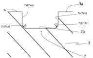
- the "arc portion” may include not only a part of a perfect circle but also a part of an ellipse and have an arc shape as a whole. For example, a part of a shape in which the corners of a polygon are rounded. It may be. That is, the arc portion may be a portion having a curved shape in the cross section of the trench, and may be provided at least in a part between the side surface and the bottom surface. For example, an example of an arc portion is shown in FIG.
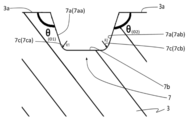
- the crystalline oxide semiconductor shown in FIG. 2 includes an arc portion 7c having two radii of curvature.
- both R1 and R2 have a radius of curvature in the range of 100 nm to 500 nm.
- the trench may have an arc portion in the entire space between the bottom surface 7b and the side surface 7a of the trench.
- the radius of curvature R1 of the first arc portion 7 ca between the bottom surface 7b of the trench 7 and the first side surface 7aa, and the bottom surface 7b and the second side surface 7ab of the trench.
- the difference between the second arc portion 7cc and the radius of curvature R2 is preferably in the range of 0 to 200 nm, and more preferably in the range of 0 to 50 nm. In the embodiment of the present invention, it is most preferable that the radius of curvature R1 of the first arc portion 7ca and the radius of curvature R2 of the second arc portion 7cc are equal.
- the "angle formed by the side surface and the first surface of the crystalline oxide semiconductor layer” is the side surface of the trench provided on the first surface 3a side of the crystalline oxide semiconductor layer 3 in the trench 7 cross section.
- the angle formed by 7a and the first surface 3a of the crystalline oxide semiconductor layer 3 is usually about 90 ° or more in the embodiment of the present invention.
- Examples of such an "angle formed by the side surface and the first surface of the crystalline oxide semiconductor layer” include an angle represented by ⁇ ( ⁇ 1, ⁇ 2) in FIGS. 14 and 16-b. ..
- the angle ⁇ 1 formed by the first side surface 7aa of the trench 7 and the first surface 3a of the crystalline oxide semiconductor layer, the second side surface 7ab of the trench 7, and the crystalline oxidation By having the angle ⁇ 2 formed by the first surface 3a of the physical semiconductor layer 3, an excellent electric field relaxation effect can be realized and the on-resistance can be lowered. Further, the upper limit of the above-mentioned "angle formed by the side surface and the first surface of the crystalline oxide semiconductor layer" is not limited as long as the object of the present invention is not impaired, but is preferably 150 °.
- the angle ( ⁇ 1) formed by the first side surface 7aa of the trench 7 and the first surface 3a of the crystalline oxide semiconductor layer and the trench 7 It is preferable that the angle ( ⁇ 2) formed by the second side surface 7ab is equal.
- the trench is formed in the crystalline oxide semiconductor layer, and is not particularly limited as long as the object of the present invention is not impaired.
- the depth of the trench is not particularly limited, but in the present invention, the depth of the trench in the cross section of the trench is usually 200 nm or more, preferably 500 nm or more, and more preferably 1 ⁇ m or more.
- the upper limit of the depth of the trench is not particularly limited, but is preferably 100 ⁇ m, and more preferably 10 ⁇ m.
- the width of the trench in the cross section of the trench is also not particularly limited, but is usually 200 nm or more, preferably 500 nm or more.
- the upper limit of the width of the trench is not particularly limited, but is preferably 100 ⁇ m, and more preferably 10 ⁇ m.
- the trench in such a preferable range, it is possible to exhibit more excellent semiconductor characteristics as a semiconductor device such as a power device.
- a semiconductor device such as a power device.
- the width of the trench is narrowed toward the bottom surface is given as a preferable example, and according to such a preferable example, It is preferable because a good interface can be formed and better electrical characteristics can be obtained.
- the side surface of the trench is tapered and the side surface has a taper angle with respect to the first surface of the crystalline oxide semiconductor layer.
- the taper angle was defined as a virtual surface (taper angle 0 ° because it does not have a taper shape) perpendicular to the first surface of the crystalline oxide semiconductor layer and the first surface in the trench cross section. In some cases, it refers to the angle formed by the virtual surface and the side surface (having a tapered shape) of the trench. Examples of the taper angle include an angle represented by ⁇ ( ⁇ 3, ⁇ 4) in FIG. In the present invention, the taper angle is preferably in the range of more than 0 ° and 45 ° or less. That is, the angle formed by the side surface and the first surface of the crystalline oxide semiconductor layer (for example, ⁇ 1 and ⁇ 2 shown in FIGS.
- the electrode may be a known one, and may be any of, for example, a Schottky electrode, an ohmic electrode, a gate electrode, a drain electrode, a source electrode, and the like.
- the electrode may be a known electrode that is appropriately set depending on the type of the semiconductor device or the like, and examples of the electrode material include D block metal and the like.
- the electrode may be referred to as a barrier electrode, for example.
- the barrier electrode is not particularly limited as long as it forms a Schottky barrier having a predetermined barrier height at the interface with the semiconductor region.
- the electrode material of the barrier electrode is not particularly limited as long as it can be used as a barrier electrode, and may be a conductive inorganic material or a conductive organic material.
- the electrode material is preferably metal.
- the metal is not particularly limited, but preferably, for example, at least one metal selected from the 4th to 11th groups of the periodic table can be mentioned.
- the metal of Group 4 of the periodic table include titanium (Ti), zirconium (Zr), hafnium (Hf), and the like, and Ti is preferable.
- the metal of Group 5 of the periodic table include vanadium (V), niobium (Nb), and tantalum (Ta).
- Examples of the metal of Group 6 of the periodic table include one or more metals selected from chromium (Cr), molybdenum (Mo), tungsten (W) and the like. Cr is preferable because the semiconductor characteristics such as switching characteristics become better.
- Examples of the metal of Group 7 of the periodic table include manganese (Mn), technetium (Tc), and rhenium (Re).
- Examples of the metal of Group 8 of the periodic table include iron (Fe), ruthenium (Ru), and osmium (Os).
- Examples of the metal of Group 9 of the periodic table include cobalt (Co), rhodium (Rh), and iridium (Ir).
- Examples of the metal of Group 10 of the periodic table include nickel (Ni), palladium (Pd), platinum (Pt), and the like, and Pt is preferable.
- Examples of the metal of Group 11 of the periodic table include copper (Cu), silver (Ag), and gold (Au).
- Examples of the means for forming the barrier electrode include known means, and more specifically, examples include a dry method and a wet method.
- Examples of the dry method include known means such as sputtering, vacuum deposition, and CVD.
- Examples of the wet method include screen printing and die coating.
- the crystalline oxide semiconductor layer is not particularly limited as long as it forms a semiconductor region in the semiconductor device.
- the crystalline oxide semiconductor layer (hereinafter, also simply referred to as “semiconductor region”) is not particularly limited as long as it contains a semiconductor as a main component, but in the present invention, the semiconductor region is a crystalline oxide semiconductor. Is preferably contained as a main component, and more preferably an n-type semiconductor region containing an n-type semiconductor as a main component.
- the crystalline oxide semiconductor preferably has a ⁇ -gaul structure or a corundum structure, and more preferably has a corundum structure.
- the semiconductor region preferably contains at least gallium, more preferably contains a gallium compound as a main component, more preferably contains an InAlGaO-based semiconductor as a main component, and ⁇ -Ga 2 O 3 or a mixed crystal thereof. Is most preferable to be contained as a main component.
- the "main component" is, for example, when the crystalline oxide semiconductor is ⁇ -Ga 2 O 3 , the atomic ratio of gallium in the metal element in the semiconductor region is 0.5 or more, and ⁇ -Ga. It is sufficient if 2 O 3 is included.
- the atomic ratio of gallium in the metal element in the semiconductor region is preferably 0.7 or more, more preferably 0.8 or more.
- the semiconductor region is usually a single-phase region, but may have a second semiconductor region or another phase composed of a different semiconductor phase as long as the object of the present invention is not impaired.
- the semiconductor region is usually in the form of a film, and may be a semiconductor film.
- the thickness of the semiconductor film in the semiconductor region is not particularly limited and may be 1 ⁇ m or less or 1 ⁇ m or more, but in the present invention, it is preferably 1 ⁇ m to 40 ⁇ m, and 1 ⁇ m to 1 ⁇ m. It is more preferably 25 ⁇ m.
- the withstand voltage of the crystalline oxide semiconductor layer is increased by, for example, making it a thick film or lowering the carrier concentration.
- the gallium oxide-based crystalline oxide semiconductor layer containing ⁇ -Ga 2 O 3 and ⁇ -Ga 2 O 3 has an arc portion having a radius of curvature in the range of 100 nm to 500 nm.
- the electric field relaxation effect is obtained by having a trench including the trench and having an angle formed by the side surface of the trench and the first surface of the crystalline oxide semiconductor layer within a range of more than 90 ° and not more than 135 °. Sufficiently obtained.
- the thickness of the gallium oxide-based crystalline oxide semiconductor layer (including the drift region) is reduced (for example, 10 ⁇ m or less). Even with such a thickness, a semiconductor device having a high withstand voltage (for example, 3000 V or more) can be realized. Further, according to the embodiment of the present invention, the thickness of the gallium oxide-based crystalline oxide semiconductor layer (including the drift region) can be further reduced (for example, 2.0 ⁇ m or less). Even with a thickness, a semiconductor device having a high withstand voltage (for example, 600 V or more) can be realized.
- the carrier concentration of the gallium oxide-based crystalline oxide semiconductor layer can be 5.0 ⁇ 10 16 / cm 3 or more, which is preferable. , 3.0 ⁇ 10 17 / cm 3 or more.
- the thickness of the crystalline oxide layer and the carrier concentration are appropriately adjusted according to the required pressure resistance, but in the embodiment of the present invention, as described above, even if the thickness is thinner or the carrier concentration is higher than before, the pressure resistance is high. As a result, the on-resistance can be lowered.
- the surface area of the semiconductor film is not particularly limited, and may be 1 mm 2 or more, may be 1 mm 2 or less.
- the crystalline oxide semiconductor is usually a single crystal, but may be a polycrystal. Further, the semiconductor film may be a single-layer film or a multilayer film. When the semiconductor film is a multilayer film, the multilayer film preferably has a thickness of 40 ⁇ m or less, and is a multilayer film including at least a first semiconductor layer and a second semiconductor layer. When the Schottky electrode is provided on the first semiconductor layer, it is also preferable that the carrier concentration of the first semiconductor layer is smaller than the carrier concentration of the second semiconductor layer.
- the second semiconductor layer usually contains a dopant, and the carrier concentration of the semiconductor layer (including the first semiconductor layer and the second semiconductor layer) adjusts the doping amount. By doing so, it can be set as appropriate.
- the semiconductor film preferably contains a dopant.
- the dopant is not particularly limited and may be a known one. Examples of the dopant include n-type dopants such as tin, germanium, silicon, titanium, zirconium, vanadium and niobium, and p-type dopants. In the present invention, the dopant is preferably Sn, Ge or Si.
- the content of the dopant is preferably 0.00001 atomic% or more, more preferably 0.00001 atomic% to 20 atomic%, and 0.00001 atomic% to 10 atomic% in the composition of the semiconductor film. Is most preferable.
- the dopant used for the first semiconductor layer is germanium, silicon, titanium, zirconium, vanadium or niobium
- the dopant used for the second semiconductor layer is tin, which provides adhesion. It is preferable because the semiconductor characteristics are further improved without impairing.
- the semiconductor film is formed by, for example, a means such as a mist CVD method, and more specifically, for example, the raw material solution is atomized (atomization step), and the obtained atomized droplets (including mist) are carried.
- a semiconductor film containing a crystalline oxide semiconductor as a main component is laminated on the substrate by transporting the atomized droplets to the substrate with gas (transportation step) and then thermally reacting the atomized droplets in the film forming chamber (conveying step). It is suitably formed by the film forming step).
- the raw material solution is atomized, the atomized droplets are suspended, and atomized droplets are generated.
- the method for atomizing the raw material solution is not particularly limited as long as the raw material solution can be atomized, and may be a known means, but in the present invention, the atomization method using ultrasonic waves is preferable.
- Atomized droplets obtained using ultrasonic waves have a zero initial velocity and are preferable because they float in the air. For example, instead of spraying them like a spray, they float in space and are transported as gas. Since it is possible, it is not damaged by collision energy, so it is very suitable.
- the droplet size is not particularly limited and may be a droplet of about several mm, but is preferably 50 ⁇ m or less, and more preferably 100 nm to 10 ⁇ m.
- the raw material solution is not particularly limited as long as it contains a raw material capable of atomizing and forming a semiconductor region, and may be an inorganic material or an organic material, but in the present invention, it may be an inorganic material or an organic material.
- the raw material is preferably a metal or a metal compound, and is selected from gallium, iron, indium, aluminum, vanadium, titanium, chromium, rhodium, nickel, cobalt, zinc, magnesium, calcium, silicon, yttrium, strontium and barium. More preferably, it contains one or more metals.
- a solution in which the metal is dissolved or dispersed in an organic solvent or water in the form of a complex or a salt can be preferably used.
- the form of the complex include an acetylacetonate complex, a carbonyl complex, an ammine complex, and a hydride complex.
- the salt form include organic metal salts (for example, metal acetate, metal oxalate, metal citrate, etc.), metal sulfide salts, nitrified metal salts, phosphor oxide metal salts, and metal halide metal salts (for example, metal chloride). Salts, metal bromide salts, metal iodide salts, etc.) and the like.
- an additive such as a hydrohalic acid or an oxidizing agent with the raw material solution.
- the hydrohalic acid include hydrobromic acid, hydrochloric acid, and hydroiodic acid. Among them, hydrobromic acid or hydroiodic acid because a better quality film can be obtained. Is preferable.
- the oxidizing agent include hydrogen peroxide (H 2 O 2 ), sodium peroxide (Na 2 O 2 ), barium peroxide (BaO 2 ), benzoyl peroxide (C 6 H 5 CO) 2 O 2 and the like. Examples include hydrogen peroxide, hypochlorous acid (HClO), perchloric acid, nitric acid, ozone water, and organic peroxides such as peracetic acid and nitrobenzene.
- the raw material solution may contain a dopant. Doping can be performed satisfactorily by including the dopant in the raw material solution.
- the dopant is not particularly limited as long as it does not interfere with the object of the present invention.
- Examples of the dopant include n-type dopants such as tin, germanium, silicon, titanium, zirconium, vanadium and niobium, and p-type dopants.
- the concentration of the dopant may usually be about 1 ⁇ 10 16 / cm 3 to 1 ⁇ 10 22 / cm 3 , and the concentration of the dopant should be as low as about 1 ⁇ 10 17 / cm 3 or less, for example. You may.
- the dopant may be contained in a high concentration of about 1 ⁇ 10 20 / cm 3 or more. In the embodiment of the present invention, it is preferably contained at a carrier concentration of 1 ⁇ 10 17 / cm 3 or more. Further, as one of the embodiments of the present invention, in a semiconductor device having a withstand voltage of 600 V, the carrier concentration of the gallium oxide-based crystalline oxide semiconductor layer is 1 ⁇ 10 17 / cm 3 or more and 3 ⁇ 10 17 / cm 3 It can be as follows.
- the solvent of the raw material solution is not particularly limited, and may be an inorganic solvent such as water, an organic solvent such as alcohol, or a mixed solvent of an inorganic solvent and an organic solvent.
- the solvent preferably contains water, and more preferably water or a mixed solvent of water and alcohol.
- the atomized droplets are transported into the film forming chamber by using a carrier gas.
- the carrier gas is not particularly limited as long as the object of the present invention is not impaired, and for example, an inert gas such as oxygen, ozone, nitrogen or argon, or a reducing gas such as hydrogen gas or forming gas is a suitable example. Can be mentioned.
- the type of the carrier gas may be one type, but may be two or more types, and a diluted gas having a reduced flow rate (for example, a 10-fold diluted gas) or the like is further used as the second carrier gas. May be good.
- the carrier gas may be supplied not only at one location but also at two or more locations.
- the flow rate of the carrier gas is not particularly limited, but is preferably 0.01 to 20 L / min, and more preferably 1 to 10 L / min.
- the flow rate of the diluting gas is preferably 0.001 to 2 L / min, more preferably 0.1 to 1 L / min.
- the semiconductor film is formed on the substrate by thermally reacting the atomized droplets in the film forming chamber.
- the thermal reaction may be such that the atomized droplets react with heat, and the reaction conditions and the like are not particularly limited as long as the object of the present invention is not impaired.
- the thermal reaction is usually carried out at a temperature equal to or higher than the evaporation temperature of the solvent, but is preferably not too high (for example, 1000 ° C.) or lower, more preferably 650 ° C. or lower, and most preferably 300 ° C. to 650 ° C. preferable.
- the thermal reaction may be carried out in any of vacuum, non-oxygen atmosphere, reducing gas atmosphere and oxygen atmosphere as long as the object of the present invention is not impaired, but the thermal reaction may be carried out in a non-oxygen atmosphere or oxygen. It is preferably performed in an atmosphere. Further, it may be carried out under any conditions of atmospheric pressure, pressurization and depressurization, but in the present invention, it is preferably carried out under atmospheric pressure.
- the film thickness can be set by adjusting the film formation time.
- the substrate is not particularly limited as long as it can support the semiconductor film.
- the material of the substrate is not particularly limited as long as it does not impair the object of the present invention, and may be a known substrate, an organic compound, or an inorganic compound.
- the shape of the substrate may be any shape and is effective for any shape, for example, plate-like, fibrous, rod-like, columnar, prismatic, such as a flat plate or a disk. Cylindrical, spiral, spherical, ring-shaped and the like can be mentioned, but in the embodiment of the present invention, a substrate is preferable.
- the thickness of the substrate is not particularly limited in the present invention.
- the substrate is not particularly limited as long as it has a plate shape and serves as a support for the semiconductor film. It may be an insulator substrate, a semiconductor substrate, a metal substrate or a conductive substrate, but the substrate is preferably an insulator substrate, and the surface is made of metal. A substrate having a film is also preferable.
- the substrate includes, for example, a base substrate containing a substrate material having a corundum structure as a main component, a substrate substrate containing a substrate material having a ⁇ -gaul structure as a main component, and a substrate material having a hexagonal structure as a main component. Examples include a base substrate.
- the “main component” means that the substrate material having the specific crystal structure is preferably 50% or more, more preferably 70% or more, still more preferably 90% or more, in terms of atomic ratio, with respect to all the components of the substrate material. It means that it is contained in% or more, and may be 100%.
- the substrate material is not particularly limited and may be a known one as long as the object of the present invention is not impaired.
- Examples of the substrate material having the corundum structure are ⁇ -Al 2 O 3 (sapphire substrate) or ⁇ -Ga 2 O 3 , and a-plane sapphire substrate, m-plane sapphire substrate, and r-plane sapphire substrate are preferable.
- C-plane sapphire substrate, ⁇ -type gallium oxide substrate (a-plane, m-plane or r-plane) and the like are more preferable examples.
- the base substrate containing the substrate material having a ⁇ -gaul structure as a main component for example, ⁇ -Ga 2 O 3 substrate or Ga 2 O 3 and Al 2 O 3 are included, and Al 2 O 3 is more than 0 wt%.
- Examples thereof include a mixed crystal substrate having a content of 60 wt% or less.
- Examples of the base substrate containing a substrate material having a hexagonal structure as a main component include a SiC substrate, a ZnO substrate, and a GaN substrate.
- an annealing treatment may be performed after the film forming step.
- the annealing treatment temperature is not particularly limited as long as the object of the present invention is not impaired, and is usually 300 ° C. to 650 ° C., preferably 350 ° C. to 550 ° C.
- the annealing treatment time is usually 1 minute to 48 hours, preferably 10 minutes to 24 hours, and more preferably 30 minutes to 12 hours.
- the annealing treatment may be carried out in any atmosphere as long as the object of the present invention is not impaired, but it is preferably in a non-oxygen atmosphere, and more preferably in a nitrogen atmosphere.
- the semiconductor film may be provided directly on the substrate, or the semiconductor film may be provided via another layer such as a buffer layer (buffer layer) or a stress relaxation layer. You may.
- the means for forming each layer is not particularly limited and may be a known means, but in the embodiment of the present invention, the mist CVD method is preferable.
- the crystalline oxide semiconductor layer contains at least gallium. Further, as one of the preferred embodiments, it is preferable that the crystalline oxide semiconductor layer has a corundum structure.
- the semiconductor film may be used in a semiconductor device as the semiconductor region after using a known means such as peeling from the substrate or the like, or may be used as it is in the semiconductor device as the semiconductor region. You may use it. Further, as one of the preferred embodiments, it is preferable that the crystalline oxide semiconductor layer contains two or more of the trenches.
- the width of the trench is preferably 2 ⁇ m or less, and it is more preferable that the crystalline oxide semiconductor layer contains 4 or more of the trenches.
- the plurality of trenches are arranged on the first surface side of the crystalline oxide semiconductor at intervals from each other.
- the semiconductor device is more suitable as a power device, and more excellent semiconductor characteristics can be obtained.
- it will be more effective for miniaturization of semiconductor devices.
- the crystalline oxide semiconductor layer has at least one arc portion between the bottom surface and the side surface of the trench, and the radius of curvature of the arc portion is in the range of 100 nm to 500 nm.
- the radius of curvature of at least one arc portion is within the range of 100 nm to 500 nm.
- the radius of curvature of the two or more arc portions is preferably in the range of 100 nm to 500 nm, and all arcs. It is more preferable that the radius of curvature of the portion is in the range of 100 nm to 500 nm.
- At least one trench 7 is provided on the first surface 3a side of the crystalline oxide semiconductor layer 3 (also referred to as a semiconductor region).
- the trench 7 includes a bottom surface, a side surface, and at least one arc portion between the bottom surface and the side surface.
- the crystalline oxide semiconductor layer 3 is electrically connected to the electrode.
- FIG. 1 shows a junction barrier Schottky diode (JBS) as a semiconductor device which is one of the embodiments of the present invention.
- JBS junction barrier Schottky diode
- the barrier height adjusting region 1 includes a barrier electrode 2 provided on the semiconductor region 3 and capable of forming a Schottky barrier between the semiconductor region 3, and the barrier electrode 2 and the semiconductor region 3. It includes a barrier height region provided between the semiconductor regions 3 and capable of forming a Schottky barrier having a barrier height larger than that of the Schottky barrier of the barrier electrode 2.
- the barrier height adjusting region 1 is embedded in a trench 7 provided on the first surface 3a side of the semiconductor region 3. In the embodiment of the present invention, it is preferable that a plurality of trenches 7 and a plurality of barrier height adjusting regions 1 arranged in the plurality of trenches 7 are provided at regular intervals, and both ends of the barrier electrode and the semiconductor region are provided.
- the barrier height adjusting regions are provided between the two.
- the JBS is configured so as to be excellent in thermal stability and adhesion, the leakage current is further reduced, and the semiconductor characteristics such as withstand voltage are further excellent.
- the semiconductor device of FIG. 1 includes an ohmic electrode 4 on the second surface 3b side of the semiconductor region 3.
- the semiconductor device of FIG. 1 has an arc portion 7c between the bottom surface 7a and the side surface 7b of the trench 7, and the radius of curvature of the arc portion is in the range of 100 nm to 500 nm, and the electric field relaxation effect is excellent. As a result, the on-resistance can be lowered.
- each layer of the semiconductor device of FIG. 1 is not particularly limited as long as the object of the present invention is not impaired, and may be known means. Examples thereof include a means of forming a film by a vacuum vapor deposition method, a CVD method, a sputtering method, various coating techniques, and the like, and then patterning by a photolithography method, or a means of directly patterning by using a printing technique or the like.
- FIG. 9 shows an example of a Schottky barrier diode (SBD) according to an embodiment of the present invention.
- the SBD of FIG. 9 includes an n-type semiconductor layer 101a, an n + type semiconductor layer 101b, a dielectric layer 104, a Schottky electrode 105a, and an ohmic electrode 105b. Further, the SBD of FIG. 9 has a trench structure including the arc portion, and the p-type semiconductor layer 102 is embedded in the trench 7.
- the material of the Schottky electrode and the ohmic electrode may be a known electrode material, and the electrode material includes, for example, Al, Mo, Co, Zr, Sn, Nb, Fe, Cr, Ta, Ti, Au, etc.
- Metals such as Pt, V, Mn, Ni, Cu, Hf, W, Ir, Zn, In, Pd, Nd or Ag or alloys thereof, tin oxide, zinc oxide, indium oxide, indium tin oxide (ITO), oxidation Examples thereof include metal oxide conductive films such as indium tin oxide (IZO), organic conductive compounds such as polyaniline, polythiophene or polypyrrole, or mixtures thereof.
- the Schottky electrode and the ohmic electrode can be formed by a known means such as a vacuum deposition method or a sputtering method. More specifically, for example, when forming a Schottky electrode, a layer made of Mo and a layer made of Al are laminated, and the layer made of Mo and the layer made of Al are patterned using a photolithography technique. It can be done by.
- the depletion layer (not shown) is contained in the n-type semiconductor layer 101a as the crystalline oxide semiconductor layer due to the stress relaxation action of the arc portion of the trench 7. Since it spreads well, it becomes a high withstand voltage SBD. Further, when a forward bias is applied, the position is located on the first surface side of the crystalline oxide semiconductor layer from the ohmic electrode 105b located on the second surface side opposite to the first surface side of the crystalline oxide semiconductor layer. Electrons flow to the Schottky electrode 105a.
- the SBD using the semiconductor structure in this way is excellent for high withstand voltage and large current, has a high switching speed, and is also excellent in withstand voltage and reliability.
- Examples of the material of the dielectric layer 104 include GaO, AlGaO, InAlGaO, AlInZnGaO 4 , AlN, Hf 2 O 3 , SiN, SiON, Al 2 O 3 , MgO, GdO, SiO 2 or Si 3 N 4. Be done. By using such an insulator for the insulator layer, the function of the semiconductor property at the interface can be satisfactorily exhibited.
- the dielectric layer 104 is provided between the n-type semiconductor layer 101 and the Schottky electrode 105a.
- the insulator layer can be formed by a known means such as a sputtering method, a vacuum vapor deposition method, or a CVD method.
- FIG. 10 shows an n-type semiconductor layer 101a as a crystalline oxide semiconductor layer, which has two or more trenches 7 arranged on the first surface side of the n-type semiconductor layer 101a.
- An example of an embodiment of a trench type Schottky barrier diode (SBD) including a semiconductor layer 101a, an n + type semiconductor layer 101b, a dielectric layer 104, a Schottky electrode 105a, and an ohmic electrode 105b is shown.
- the trench-type SBD of FIG. 10 has a trench structure including the arc portion. According to such a trench type SBD, the leakage current can be significantly reduced while maintaining a higher withstand voltage, and as a result, a significantly lower on-resistance can be achieved.
- FIG. 11 shows the implementation of a junction barrier Schottky diode (JBS) including an n-type semiconductor layer 101a, an n + type semiconductor layer 101b, a p-type semiconductor layer 102, a dielectric layer 104, a Schottky electrode 105a, and an ohmic electrode 105b.
- JBS junction barrier Schottky diode
- the JBS of FIG. 11 has a trench 7 having the arc portion, and the p-type semiconductor layer 102 is embedded in the trench structure. According to such a JBS, the leakage current can be significantly reduced while maintaining a higher withstand voltage than the trench type SBD of FIG. 10, and as a result, a significantly lower on-resistance can be achieved. It will be possible.
- FIG. 12 shows an example of an embodiment when the semiconductor device is a MOSFET.
- the MOSFET in FIG. 12 is a trench-type MOSFET, which is an n-type semiconductor layer 131a as a crystalline oxide semiconductor layer, and the n-type semiconductor layer 131a, the n + -type semiconductor layers 131b, and 131c including the trench 7. , A gate insulating film 134, and a gate electrode 135a, a source electrode 135b, and a drain electrode 135c.
- n + type semiconductor layer 131b having a thickness of, for example, 100 nm to 100 ⁇ m is formed on the drain electrode 135c, and an n-type semiconductor layer 131a having a thickness of, for example, 100 nm to 100 ⁇ m is formed on the n + type semiconductor layer 131b.
- an n + type semiconductor layer 131c is formed on the n ⁇ type semiconductor layer 131a, and a source electrode 135b is formed on the n + type semiconductor layer 131c.
- grooves are formed as a plurality of trenches 7 having a depth that penetrates the n + semiconductor layer 131c and reaches halfway through the n-type semiconductor layer 131a. It is formed.
- Each of such trenches 7 is provided with the arc portion between the bottom surface and the side surface of the trench 7.
- a gate electrode 135a is embedded in the trench 7 via, for example, a gate insulating film 134 having a thickness of 10 nm to 1 ⁇ m.
- the n ⁇ type is applied.
- a channel layer is formed on the side surface of the semiconductor layer 131a, and electrons are injected into the n-type semiconductor layer to turn on.
- the off state by setting the voltage of the gate electrode to 0V, the channel layer cannot be formed, the n-type semiconductor layer is filled with the depletion layer, and the turn-off occurs.
- a known means can be appropriately used for manufacturing the MOSFET of FIG. 12.
- an etching mask is provided in a predetermined region of the n-type semiconductor layer 131a and the n + type semiconductor layer 131c, and etching is performed by the above-mentioned preferable high-pressure dry etching method to perform the etching from the surface of the n-type semiconductor layer 131c to the n-type semiconductor layer.
- a groove of the trench 7 having a depth reaching the middle of 131a is formed together with the arc portion.
- a gate insulating film 134 having a thickness of, for example, 50 nm to 1 ⁇ m is formed on the side surface and the bottom surface of the groove of the trench 7 by using known means such as a thermal oxidation method, a vacuum vapor deposition method, a sputtering method, and a CVD method.
- a gate electrode material such as polysilicon is formed in the groove of the trench 7 at a thickness equal to or less than the thickness of the n-type semiconductor layer by using a CVD method, a vacuum vapor deposition method, a sputtering method, or the like.
- the source electrode 135b is formed on the n + type semiconductor layer 131c and the drain electrode 135c is formed on the n + type semiconductor layer 131b by using known means such as a vacuum deposition method, a sputtering method, and a CVD method.
- Power MOSFETs can be manufactured.
- the electrode materials of the source electrode and the drain electrode may be known electrode materials, respectively, and the electrode materials include, for example, Al, Mo, Co, Zr, Sn, Nb, Fe, Cr, Ta, and Ti.
- FIG. 12 shows an example of a trench-type vertical MOSFET
- the present invention is not limited to this, and can be applied to various forms of a trench-type MOSFET.
- the depth of the groove of the trench 7 in FIG. 12 may be dug down to a depth reaching the bottom surface of the n-type semiconductor layer 131a to reduce the series resistance.
- FIG. 12 shows an example of another trench-type MOSFET is shown in FIG.
- FIG. 13 shows an n ⁇ type semiconductor layer 131a, a first n + type semiconductor layer 131b, a second n + type semiconductor layer 131c, a p-type semiconductor layer 132, a p + type semiconductor layer 132a, a gate insulating film 134, and a gate electrode 135a.
- An example of an embodiment of a metal oxide semiconductor field effect transistor (MOSFET) including a source electrode 135b and a drain electrode 135c is shown.
- the p + type semiconductor layer 132a may be a p-type semiconductor layer or may be the same as the p-type semiconductor layer 132.
- the semiconductor device is particularly preferably a power device. Further, as one of the embodiments, it is preferable that the semiconductor device is a vertical device. Examples of the semiconductor device include a diode or a transistor (for example, MESFET), and among them, a diode is preferable, and a junction barrier Schottky diode (JBS) is more preferable.
- a diode or a transistor for example, MESFET
- JBS junction barrier Schottky diode
- the semiconductor device is preferably used as a power module, an inverter or a converter by using known means, and further preferably used for a semiconductor system using, for example, a power supply device.
- the power supply device can be manufactured from the semiconductor device or as the semiconductor device by connecting to a wiring pattern or the like by using a known means.
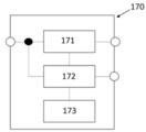
- the power supply system 170 is configured by using the plurality of power supply devices 171 and 172 and the control circuit 173.
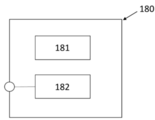
- the power supply system can be used in the system apparatus 180 by combining the electronic circuit 181 and the power supply system 182.
- An example of the power supply circuit diagram of the power supply device is shown in FIG. FIG.
- FIG. 5 shows a power supply circuit of a power supply device including a power circuit and a control circuit.
- the DC voltage is switched at a high frequency by an inverter 192 (composed of MOSFETs A to D), converted to AC, and then insulated and transformed by a transformer 193.
- an inverter 192 composed of MOSFETs A to D
- DCL195 smoothing coils L1 and L2
- a capacitor smoothing coils L1 and L2
- a DC voltage is output.
- the voltage comparator 197 compares the output voltage with the reference voltage
- the PWM control circuit 196 controls the inverter 192 and the rectifier MOSFET 194 so as to obtain a desired output voltage.
- Example 1 Formation of semiconductor layer 1-1.
- Film formation device The mist CVD device 19 used in the examples will be described with reference to FIG.
- the film forming apparatus 19 of FIG. 6 supplies a carrier gas source 22a for supplying a carrier gas, a flow control valve 23a for adjusting the flow rate of the carrier gas sent out from the carrier gas source 22a, and a carrier gas (diluted).
- Preparation for film formation 1-2 The raw material solution 24a obtained in 1) was housed in the mist generation source 24. Next, as the substrate 20, a sapphire substrate was placed on the susceptor 21, and the heater 28 was operated to raise the temperature inside the film forming chamber 30 to 630 ° C. Next, the flow rate control valves 23a and 23b are opened, carrier gas is supplied into the film forming chamber 30 from the carrier gas supply means 22a and 22b which are carrier gas sources, and the atmosphere of the film forming chamber 30 is sufficiently filled with the carrier gas. After the replacement, the flow rate of the carrier gas was adjusted to 1 L / min, and the flow rate of the carrier gas (dilution) was adjusted to 2 L / min. Nitrogen was used as the carrier gas.
- the ultrasonic transducer 26 was vibrated at 2.4 MHz, and the vibration was propagated to the raw material solution 24a through water 25a to atomize the raw material solution 24a to generate mist.
- This mist was introduced into the film forming chamber 30 by the carrier gas, and the mist reacted in the film forming chamber 30 at 630 ° C. under atmospheric pressure to form a semiconductor film on the substrate 20.
- the film thickness was 4.1 ⁇ m, and the film formation time was 105 minutes.
- Etching A trench was formed in the semiconductor film using an ICP-RIE apparatus under the conditions shown in Table 1 below.
- Each of the trenches of the examples had an arc portion, and the radius of curvature of the arc portion was in the range of 100 nm or more and 500 nm or less.
- a cross-sectional photograph of the trench formed as Example 1 is shown in FIG.
- the radius of curvature of Example 1 was 140 nm for R1 (left side) and 160 nm for R2 (right side).
- the side surface of the trench had a taper angle, and the taper angle was 60 °.
- a good trench was formed. Further, the tendency for such a good trench to be formed was observed in the pressure range of 1 Pa to 10 Pa, particularly 2 Pa to 10 Pa, other than the pressure of 5 Pa.
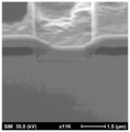
- Example 2 A trench was formed in the same manner as in Example 1 except that the etching was performed under the conditions shown in Table 1.
- a cross-sectional photograph of the obtained trench is shown in FIG.
- the radius of curvature of the arc portion of the trench was 125 nm for R1 (left side) and 298 nm for R2 (right side).
- a trench having a good quality arc portion was formed.
- Example 3 A trench was formed in the semiconductor film (also referred to as a crystalline oxide semiconductor layer) in the same manner as in Example 1 except that the etching was performed under the conditions shown in Table 2.
- a cross-sectional photograph of the obtained trench is shown in FIG. 16-a. Further, FIG. 16-b shows an explanatory view using the same cross-sectional photograph.
- the radius of curvature R1 (left side) of the first arc portion 7ca of the trench 7 was 220 nm
- the radius of curvature R2 (right side) of the second arc portion 7cc was also 220 nm.
- a plurality of trenches 7 were formed in the crystalline oxide semiconductor layer 3, and in each of the trenches 7, trenches 7 having the same radius of curvature of the first arc portion 7ca and the second arc portion 7cc were formed.
- the width of the trench 7 narrows toward the bottom surface.
- the angle ( ⁇ 1 shown in FIG. 16-b) formed by the side surface 7a (first side surface 7aa) of the trench and the first surface 3a of the crystalline oxide semiconductor layer 3 exceeds 90 °.
- the angle between the side surface 7a (second side surface 7ab) of the trench and the first surface 3a of the crystalline oxide semiconductor layer 3 ( ⁇ 2 shown in FIG. 16-b) is within the range of 135 ° or less.
- SiO 2 shown in FIG. 16-b is a mask, which is provided on the crystalline oxide semiconductor layer 3 in order to perform etching to form a trench, and is finally removed. Further, when the crystalline oxide semiconductor layer was obtained by changing the flow rate of BCl 3 , it was found that a trench having a better arc portion could be obtained by setting the crystal oxide semiconductor layer in the range of 50 sccm to 100 sccm.
- the trench cross section has a trench including an arc portion having a radius of curvature in the range of 100 nm to 500 nm, and the side surface of the trench and the crystalline oxide.
- the angle formed by the first surface of the semiconductor layer exceeds 90 ° and is within the range of 135 ° or less, the electric field relaxation effect can be sufficiently obtained. As a result, it has become possible to reduce the on-resistance of the semiconductor device having the gallium oxide-based crystalline oxide semiconductor layer.
- the on-resistance of the semiconductor device can be further reduced. Can be expected.
- Example 1 A trench was formed in the same manner as in Example 1 except that etching was performed under the conditions shown in Table 1.
- the obtained trench had a convex bottom surface and had corners between the bottom surface and the side surface, so that a poor quality trench was formed.
- Example 2 A trench was formed in the same manner as in Example 1 except that etching was performed under the conditions shown in Table 1.
- the side surface of the obtained trench was hollowed out in an inverted tapered shape, and the width inside the trench was wider than the opening of the trench. Further, although an arc portion was formed between the bottom surface and the side surface, the arc portion protruded greatly and the radius of curvature was 1 ⁇ m or more, and a trench of poor quality was formed.
- the method of the present invention can be used in all fields such as semiconductors (for example, compound semiconductor electronic devices, etc.), electronic parts / electrical equipment parts, optical / electrophotographic related devices, industrial parts, etc., but is particularly useful for manufacturing power devices. Is.
Landscapes
- Electrodes Of Semiconductors (AREA)
Priority Applications (1)
| Application Number | Priority Date | Filing Date | Title |
|---|---|---|---|
| JP2021555973A JPWO2021095474A1 (https=) | 2019-11-14 | 2020-10-21 |
Applications Claiming Priority (2)
| Application Number | Priority Date | Filing Date | Title |
|---|---|---|---|
| JP2019-206571 | 2019-11-14 | ||
| JP2019206571 | 2019-11-14 |
Publications (1)
| Publication Number | Publication Date |
|---|---|
| WO2021095474A1 true WO2021095474A1 (ja) | 2021-05-20 |
Family
ID=75911350
Family Applications (1)
| Application Number | Title | Priority Date | Filing Date |
|---|---|---|---|
| PCT/JP2020/039625 Ceased WO2021095474A1 (ja) | 2019-11-14 | 2020-10-21 | 結晶性酸化物のエッチング方法およびトレンチ形成方法ならびに半導体装置の製造方法 |
Country Status (2)
| Country | Link |
|---|---|
| JP (1) | JPWO2021095474A1 (https=) |
| WO (1) | WO2021095474A1 (https=) |
Citations (9)
| Publication number | Priority date | Publication date | Assignee | Title |
|---|---|---|---|---|
| JP2000103689A (ja) * | 1998-09-28 | 2000-04-11 | Kyocera Corp | アルミナ質焼結体およびその製造方法、並びに耐プラズマ部材 |
| JP2007335505A (ja) * | 2006-06-13 | 2007-12-27 | Canon Inc | 酸化物半導体膜のドライエッチング方法 |
| JP2013077817A (ja) * | 2011-09-16 | 2013-04-25 | Semiconductor Energy Lab Co Ltd | 半導体装置 |
| JP2013179127A (ja) * | 2012-02-28 | 2013-09-09 | National Institute Of Advanced Industrial & Technology | 電子デバイスの製造方法及び薄膜トランジスタ |
| JP2015227279A (ja) * | 2014-05-08 | 2015-12-17 | 株式会社Flosfia | 結晶性積層構造体および半導体装置 |
| JP2016208024A (ja) * | 2015-04-15 | 2016-12-08 | 株式会社半導体エネルギー研究所 | 電極及び半導体装置の作製方法 |
| JP2017224794A (ja) * | 2016-06-17 | 2017-12-21 | ラピスセミコンダクタ株式会社 | 半導体装置および半導体装置の製造方法 |
| JP2018093207A (ja) * | 2014-07-22 | 2018-06-14 | 株式会社Flosfia | 結晶性半導体膜および板状体ならびに半導体装置 |
| JP2018170306A (ja) * | 2017-03-29 | 2018-11-01 | Tdk株式会社 | 酸化ガリウム半導体装置の製造方法 |
Family Cites Families (2)
| Publication number | Priority date | Publication date | Assignee | Title |
|---|---|---|---|---|
| JP6967238B2 (ja) * | 2017-02-28 | 2021-11-17 | 株式会社タムラ製作所 | ショットキーバリアダイオード |
| JP6618216B2 (ja) * | 2018-10-11 | 2019-12-11 | 国立研究開発法人物質・材料研究機構 | α−Ga2O3単結晶、α−Ga2O3の製造方法、および、それを用いた半導体素子 |
-
2020
- 2020-10-21 JP JP2021555973A patent/JPWO2021095474A1/ja active Pending
- 2020-10-21 WO PCT/JP2020/039625 patent/WO2021095474A1/ja not_active Ceased
Patent Citations (9)
| Publication number | Priority date | Publication date | Assignee | Title |
|---|---|---|---|---|
| JP2000103689A (ja) * | 1998-09-28 | 2000-04-11 | Kyocera Corp | アルミナ質焼結体およびその製造方法、並びに耐プラズマ部材 |
| JP2007335505A (ja) * | 2006-06-13 | 2007-12-27 | Canon Inc | 酸化物半導体膜のドライエッチング方法 |
| JP2013077817A (ja) * | 2011-09-16 | 2013-04-25 | Semiconductor Energy Lab Co Ltd | 半導体装置 |
| JP2013179127A (ja) * | 2012-02-28 | 2013-09-09 | National Institute Of Advanced Industrial & Technology | 電子デバイスの製造方法及び薄膜トランジスタ |
| JP2015227279A (ja) * | 2014-05-08 | 2015-12-17 | 株式会社Flosfia | 結晶性積層構造体および半導体装置 |
| JP2018093207A (ja) * | 2014-07-22 | 2018-06-14 | 株式会社Flosfia | 結晶性半導体膜および板状体ならびに半導体装置 |
| JP2016208024A (ja) * | 2015-04-15 | 2016-12-08 | 株式会社半導体エネルギー研究所 | 電極及び半導体装置の作製方法 |
| JP2017224794A (ja) * | 2016-06-17 | 2017-12-21 | ラピスセミコンダクタ株式会社 | 半導体装置および半導体装置の製造方法 |
| JP2018170306A (ja) * | 2017-03-29 | 2018-11-01 | Tdk株式会社 | 酸化ガリウム半導体装置の製造方法 |
Also Published As
| Publication number | Publication date |
|---|---|
| JPWO2021095474A1 (https=) | 2021-05-20 |
Similar Documents
| Publication | Publication Date | Title |
|---|---|---|
| JP7064724B2 (ja) | 半導体装置 | |
| JP7595966B2 (ja) | 半導体装置 | |
| JP6916426B2 (ja) | 積層構造体およびその製造方法、半導体装置ならびに結晶膜 | |
| JP7690157B2 (ja) | 半導体装置 | |
| US11495695B2 (en) | Semiconductor device | |
| JP2018129500A (ja) | 半導体装置 | |
| US12148804B2 (en) | Semiconductor device including one or more p-type semiconductors provided between an n-type semiconductor layer and an electrode | |
| JP6230196B2 (ja) | 結晶性半導体膜および半導体装置 | |
| JP6999106B2 (ja) | 半導体装置 | |
| WO2021095474A1 (ja) | 結晶性酸化物のエッチング方法およびトレンチ形成方法ならびに半導体装置の製造方法 | |
| TWI870495B (zh) | 結晶性氧化物的蝕刻方法及溝槽形成方法、以及半導體裝置的製造方法 | |
| JP6478425B2 (ja) | 結晶性半導体膜および半導体装置 | |
| JP6999103B2 (ja) | 半導体装置 | |
| JP2019016720A (ja) | 半導体装置の製造方法 | |
| JP2024079770A (ja) | 半導体装置 | |
| HK40023886A (en) | Semiconductor device | |
| JP2019016719A (ja) | 半導体装置 |
Legal Events
| Date | Code | Title | Description |
|---|---|---|---|
| 121 | Ep: the epo has been informed by wipo that ep was designated in this application |
Ref document number: 20888170 Country of ref document: EP Kind code of ref document: A1 |
|
| ENP | Entry into the national phase |
Ref document number: 2021555973 Country of ref document: JP Kind code of ref document: A |
|
| NENP | Non-entry into the national phase |
Ref country code: DE |
|
| 122 | Ep: pct application non-entry in european phase |
Ref document number: 20888170 Country of ref document: EP Kind code of ref document: A1 |