WO2021085465A1 - 弾性波装置 - Google Patents
弾性波装置 Download PDFInfo
- Publication number
- WO2021085465A1 WO2021085465A1 PCT/JP2020/040408 JP2020040408W WO2021085465A1 WO 2021085465 A1 WO2021085465 A1 WO 2021085465A1 JP 2020040408 W JP2020040408 W JP 2020040408W WO 2021085465 A1 WO2021085465 A1 WO 2021085465A1
- Authority
- WO
- WIPO (PCT)
- Prior art keywords
- layer
- elastic wave
- wave device
- electrode
- piezoelectric substrate
- Prior art date
- Legal status (The legal status is an assumption and is not a legal conclusion. Google has not performed a legal analysis and makes no representation as to the accuracy of the status listed.)
- Ceased
Links
Images


Classifications
-
- H—ELECTRICITY
- H03—ELECTRONIC CIRCUITRY
- H03H—IMPEDANCE NETWORKS, e.g. RESONANT CIRCUITS; RESONATORS
- H03H9/00—Networks comprising electromechanical or electro-acoustic elements; Electromechanical resonators
- H03H9/02—Details
- H03H9/02535—Details of surface acoustic wave devices
- H03H9/02818—Means for compensation or elimination of undesirable effects
- H03H9/02929—Means for compensation or elimination of undesirable effects of ageing changes of characteristics, e.g. electro-acousto-migration
-
- H—ELECTRICITY
- H03—ELECTRONIC CIRCUITRY
- H03H—IMPEDANCE NETWORKS, e.g. RESONANT CIRCUITS; RESONATORS
- H03H9/00—Networks comprising electromechanical or electro-acoustic elements; Electromechanical resonators
- H03H9/25—Constructional features of resonators using surface acoustic waves
-
- H—ELECTRICITY
- H03—ELECTRONIC CIRCUITRY
- H03H—IMPEDANCE NETWORKS, e.g. RESONANT CIRCUITS; RESONATORS
- H03H3/00—Apparatus or processes specially adapted for the manufacture of impedance networks, resonating circuits, resonators
- H03H3/007—Apparatus or processes specially adapted for the manufacture of impedance networks, resonating circuits, resonators for the manufacture of electromechanical resonators or networks
- H03H3/08—Apparatus or processes specially adapted for the manufacture of impedance networks, resonating circuits, resonators for the manufacture of electromechanical resonators or networks for the manufacture of resonators or networks using surface acoustic waves
-
- H—ELECTRICITY
- H03—ELECTRONIC CIRCUITRY
- H03H—IMPEDANCE NETWORKS, e.g. RESONANT CIRCUITS; RESONATORS
- H03H9/00—Networks comprising electromechanical or electro-acoustic elements; Electromechanical resonators
- H03H9/02—Details
- H03H9/02535—Details of surface acoustic wave devices
- H03H9/02543—Characteristics of substrate, e.g. cutting angles
- H03H9/02574—Characteristics of substrate, e.g. cutting angles of combined substrates, multilayered substrates, piezoelectrical layers on not-piezoelectrical substrate
-
- H—ELECTRICITY
- H03—ELECTRONIC CIRCUITRY
- H03H—IMPEDANCE NETWORKS, e.g. RESONANT CIRCUITS; RESONATORS
- H03H9/00—Networks comprising electromechanical or electro-acoustic elements; Electromechanical resonators
- H03H9/02—Details
- H03H9/02535—Details of surface acoustic wave devices
- H03H9/02818—Means for compensation or elimination of undesirable effects
-
- H—ELECTRICITY
- H03—ELECTRONIC CIRCUITRY
- H03H—IMPEDANCE NETWORKS, e.g. RESONANT CIRCUITS; RESONATORS
- H03H9/00—Networks comprising electromechanical or electro-acoustic elements; Electromechanical resonators
- H03H9/02—Details
- H03H9/02535—Details of surface acoustic wave devices
- H03H9/02818—Means for compensation or elimination of undesirable effects
- H03H9/02866—Means for compensation or elimination of undesirable effects of bulk wave excitation and reflections
-
- H—ELECTRICITY
- H03—ELECTRONIC CIRCUITRY
- H03H—IMPEDANCE NETWORKS, e.g. RESONANT CIRCUITS; RESONATORS
- H03H9/00—Networks comprising electromechanical or electro-acoustic elements; Electromechanical resonators
- H03H9/02—Details
- H03H9/125—Driving means, e.g. electrodes, coils
- H03H9/145—Driving means, e.g. electrodes, coils for networks using surface acoustic waves
-
- H—ELECTRICITY
- H03—ELECTRONIC CIRCUITRY
- H03H—IMPEDANCE NETWORKS, e.g. RESONANT CIRCUITS; RESONATORS
- H03H9/00—Networks comprising electromechanical or electro-acoustic elements; Electromechanical resonators
- H03H9/02—Details
- H03H9/125—Driving means, e.g. electrodes, coils
- H03H9/145—Driving means, e.g. electrodes, coils for networks using surface acoustic waves
- H03H9/14538—Formation
- H03H9/14541—Multilayer finger or busbar electrode
-
- H—ELECTRICITY
- H03—ELECTRONIC CIRCUITRY
- H03H—IMPEDANCE NETWORKS, e.g. RESONANT CIRCUITS; RESONATORS
- H03H9/00—Networks comprising electromechanical or electro-acoustic elements; Electromechanical resonators
- H03H9/02—Details
- H03H9/02007—Details of bulk acoustic wave devices
- H03H9/02157—Dimensional parameters, e.g. ratio between two dimension parameters, length, width or thickness
Definitions
- the present invention generally relates to an elastic wave device, and more particularly to an elastic wave device including electrodes.
- an elastic surface wave element including a piezoelectric substrate and an electrode formed on the piezoelectric substrate is known (see, for example, Patent Document 1).
- the electrode has a layer containing aluminum and copper.
- columnar crystal grains made of an aluminum-copper alloy are formed at the grain boundaries of columnar crystal grains made of aluminum.
- the surface acoustic wave element described in Patent Document 1 has a problem that when the copper concentration of the electrode is increased in order to further improve the power resistance, the electric resistance increases and the characteristics of the surface acoustic wave element tend to deteriorate. there were.
- An object of the present invention is to provide an elastic wave device capable of improving power resistance while suppressing deterioration of characteristics.
- the elastic wave device includes a piezoelectric substrate and electrodes.
- the electrodes are formed on the piezoelectric substrate.
- the electrode has a first layer and a second layer.
- the first layer contains Al and Cu.
- the second layer is formed on the side of the first layer opposite to the piezoelectric substrate side, and contains Al.
- the first layer has at least a part of Al crystals and CuAl 2 crystal grains arranged in a direction orthogonal to the thickness direction of the piezoelectric substrate. In the electrode, the CuAl 2 crystal grains do not reach the main surface of the second layer opposite to the first layer side.
- the elastic wave device includes a piezoelectric substrate and electrodes.
- the electrodes are formed on the piezoelectric substrate.
- the electrode has a first layer and a second layer.
- the first layer contains Al and Cu.
- the second layer is formed on the side of the first layer opposite to the piezoelectric substrate side, and contains Cu.
- the first layer has Al crystals and CuAl 2 crystal grains that are arranged in a direction orthogonal to the thickness direction of the piezoelectric substrate. In the electrode, the CuAl 2 crystal grains do not reach the main surface of the second layer opposite to the first layer side.
- the elastic wave device can improve the power resistance while suppressing the deterioration of characteristics.
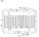
- FIG. 1 is a plan view of the elastic wave device according to the first embodiment.
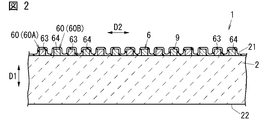
- FIG. 2 is a cross-sectional view of the elastic wave device of the same as above.
- FIG. 3 is a vertical cross-sectional view of the electrodes of the elastic wave device of the same as above.
- FIG. 4 is a cross-sectional view of the electrodes of the elastic wave device of the same as above.
- FIG. 5 is a schematic view of a STEM (Scanning Transmission Electron Microscope) image of the elastic wave device of the above.
- 6A to 6F are process cross-sectional views for explaining a method of manufacturing the elastic wave device of the same as above.
- FIG. 7 is an explanatory diagram of a method for manufacturing the elastic wave device of the same as above.
- FIG. 1 is a plan view of the elastic wave device according to the first embodiment.
- FIG. 2 is a cross-sectional view of the elastic wave device of the same as above.
- FIG. 3 is a vertical cross-sectional view of the electrode
- FIG. 8 is a graph showing the relationship between the Cu concentration of the elastic wave device as described above, the normalized resistivity, and the withstand power.
- FIG. 9 is a vertical cross-sectional view of the electrodes of the elastic wave device according to the modified example of the first embodiment.
- FIG. 10 is a vertical cross-sectional view of the elastic wave device according to the second embodiment.
- FIG. 11 is an explanatory diagram of a method for manufacturing the elastic wave device of the same as above.
- FIG. 12 is a cross-sectional view of the elastic wave device according to the third embodiment.
- FIG. 13 is a cross-sectional view of the elastic wave device according to the fourth embodiment.
- FIGS. 1 to 4, 6A to 6F, 7 and 9 to 13 referred to in the following embodiments and the like are all schematic views, and the size and thickness ratios of the respective components in the drawings are not necessarily the same. It does not always reflect the actual dimensional ratio.
- the elastic wave device 1 includes a piezoelectric substrate 2 and an IDT (Interdigital Transducer) electrode 6.
- the IDT electrode 6 is formed on the piezoelectric substrate 2.
- the IDT electrode 6 has two electrodes 60.
- the elastic wave device 1 further includes two reflectors 7.
- the two reflectors 7 are formed on the piezoelectric substrate 2.
- the two reflectors 7 are located on one side and the other side of the IDT electrode 6 in the direction along the propagation direction of the elastic wave of the elastic wave device 1.
- the elastic wave device 1 further includes a wiring portion 8 connected to the IDT electrode 6.
- the wiring portion 8 is formed on the piezoelectric substrate 2.
- the elastic wave device 1 further includes an IDT electrode 6, each reflector 7, and a protective film 9 (see FIG. 2) covering each wiring portion 8 on the piezoelectric substrate 2.
- the protective film 9 is not shown.
- the elastic wave device 1 may not be provided with the protective film 9.
- the elastic wave device 1 In the elastic wave device 1, one IDT electrode 6 is formed on the piezoelectric substrate 2, but the number of IDT electrodes 6 is not limited to one and may be plural. That is, the elastic wave device 1 may include a plurality of IDT electrodes 6. In this case, in the elastic wave device 1, for example, a plurality of elastic surface wave resonators including each of the plurality of IDT electrodes 6 may be electrically connected to form a band-passing type filter.
- the piezoelectric substrate 2 is a piezoelectric substrate.
- the material of the piezoelectric substrate is, for example, lithium tantalate (LiTaO 3 ).
- the piezoelectric substrate is formed from, for example, a ⁇ ° Y-cut X-propagated LiTaO 3 piezoelectric single crystal.
- the ⁇ ° Y-cut X-propagation LiTaO 3 piezoelectric single crystal has the X-axis as the central axis in the direction from the Y-axis to the Z-axis when the three crystal axes of the LiTaO 3 piezoelectric single crystal are the X-axis, the Y-axis, and the Z-axis. It is a LiTaO 3 single crystal cut along a plane whose normal axis is rotated by ⁇ °, and is a single crystal in which an elastic surface wave propagates in the X-axis direction.
- ⁇ and ⁇ ⁇ 180 ⁇ n are synonymous (crystallographically equivalent).
- n is a natural number.
- the piezoelectric substrate is not limited to the ⁇ ° Y-cut X-propagation LiTaO 3 piezoelectric single crystal, and may be, for example, ⁇ ° Y-cut X-propagation LiTaO 3 piezoelectric ceramics.
- the piezoelectric substrate 2 has a first main surface 21 and a second main surface 22 facing each other.
- the first main surface 21 and the second main surface 22 face each other in the thickness direction D1 of the piezoelectric substrate 2.
- the piezoelectric substrate 2 has a rectangular shape in a plan view from the thickness direction D1 of the piezoelectric substrate 2, but the piezoelectric substrate 2 is not limited to this, and may be, for example, a square shape.
- the material of the piezoelectric substrate is not limited to lithium tantalate (LiTaO 3 ), and is, for example, lithium niobate (LiNbO 3 ), zinc oxide (ZnO), aluminum nitride (AlN), or lead zirconate titanate (PZT). There may be.
- the piezoelectric substrate is made of, for example, Y-cut X-propagated LiNbO 3 piezoelectric single crystal or piezoelectric ceramics
- the elastic wave device 1 uses a love wave as an elastic wave to make a mode mainly composed of an SH wave as a main mode. Can be used as.
- the single crystal material and cut angle of the piezoelectric substrate may be appropriately determined according to, for example, the required specifications of the filter (passing characteristics, attenuation characteristics, temperature characteristics, filter characteristics such as bandwidth) and the like.
- the IDT electrode 6 is formed on the piezoelectric substrate 2. More specifically, the IDT electrode 6 is formed on the first main surface 21 of the piezoelectric substrate 2.
- the IDT electrode 6 has two electrodes 60 as described above. Each of the two electrodes 60 is conductive. The two electrodes 60 are separated from each other and are electrically isolated from each other. In the following, when the two electrodes 60 are described separately from each other, one of the two electrodes 60 will be referred to as a first electrode 60A, and the other electrode 60 will be referred to as a second electrode 60B.
- the first electrode 60A has a comb shape in a plan view from the thickness direction D1 of the piezoelectric substrate 2.
- the first electrode 60A has a first bus bar 61 and a plurality of first electrode fingers 63.
- the first bus bar 61 is a conductor portion for making a plurality of first electrode fingers 63 have the same potential.
- the second electrode 60B has a comb shape in a plan view from the thickness direction D1 of the piezoelectric substrate 2.
- the second electrode 60B has a second bus bar 62 and a plurality of second electrode fingers 64.
- the second bus bar 62 is a conductor portion for making a plurality of second electrode fingers 64 have the same potential (equal potential).
- the first bus bar 61 and the second bus bar 62 face each other.
- the plurality of first electrode fingers 63 are connected to the first bus bar 61 and extend to the second bus bar 62 side.
- the plurality of first electrode fingers 63 are formed integrally with the first bus bar 61 and are separated from the second bus bar 62.
- the plurality of second electrode fingers 64 are connected to the second bus bar 62 and extend to the first bus bar 61 side.
- the plurality of second electrode fingers 64 are formed integrally with the second bus bar 62 and are separated from the first bus bar 61.
- the IDT electrode 6 is, for example, a normal type IDT electrode. Hereinafter, the IDT electrode 6 will be described in more detail.
- the first bus bar 61 and the second bus bar 62 of the IDT electrode 6 have a long shape whose longitudinal direction is the second direction D2 orthogonal to the thickness direction D1 (first direction) of the piezoelectric substrate 2.
- the first bus bar 61 and the second bus bar 62 of the IDT electrode 6 have a long shape with the second direction D2, which is the elastic wave propagation direction, as the longitudinal direction.
- the first bus bar 61 and the second bus bar 62 face each other in the third direction D3 orthogonal to both the thickness direction D1 and the second direction D2 of the piezoelectric substrate 2.
- the first bus bar 61 and the second bus bar 62 face each other in the third direction D3, which is the direction in which the first electrode finger 63 and the second electrode finger 64, which will be described later, extend.
- the plurality of first electrode fingers 63 are connected to the first bus bar 61 and extend toward the second bus bar 62.
- the plurality of first electrode fingers 63 extend from the first bus bar 61 along the third direction D3.
- the tips of the plurality of first electrode fingers 63 and the second bus bar 62 are separated from each other.
- the plurality of first electrode fingers 63 have the same length and the same width.
- the plurality of second electrode fingers 64 are connected to the second bus bar 62 and extend toward the first bus bar 61.
- the plurality of second electrode fingers 64 extend from the second bus bar 62 along the third direction D3.
- the tips of the plurality of second electrode fingers 64 are separated from the first bus bar 61.
- the plurality of second electrode fingers 64 have the same length and the same width.
- the length of the plurality of second electrode fingers 64 is the same as the length of the plurality of first electrode fingers 63.
- the width of the plurality of second electrode fingers 64 is the same as the width of the plurality of first electrode fingers 63.
- a plurality of first electrode fingers 63 and a plurality of second electrode fingers 64 are alternately arranged one by one in the second direction D2 so as to be separated from each other. Therefore, the adjacent first electrode finger 63 and the second electrode finger 64 are separated from each other.
- a group of electrode fingers including a plurality of first electrode fingers 63 and a plurality of second electrode fingers 64 a plurality of first electrode fingers 63 and a plurality of second electrode fingers 64 are separated from each other in the second direction D2.
- the configuration may be such that the plurality of first electrode fingers 63 and the plurality of second electrode fingers 64 are not arranged alternately separated from each other. For example, a region in which the first electrode finger 63 and the second electrode finger 64 are lined up one by one, and a region in which the first electrode finger 63 or the second electrode finger 64 are lined up in the second direction D2. And may be mixed.
- the IDT electrode 6 has an intersecting region defined by a plurality of first electrode fingers 63 and a plurality of second electrode fingers 64.
- the intersecting region is an area between the envelope at the tips of the plurality of first electrode fingers 63 and the envelope at the tips of the plurality of second electrode fingers 64.
- the IDT electrode 6 excites an elastic wave on the piezoelectric substrate 2 in the intersecting region.
- the IDT electrode 6 is a normal type IDT electrode, but is not limited to this, and may be, for example, an IDT electrode to which apodization weighting is applied, or an inclined IDT electrode.
- the crossing width increases from one end in the propagation direction of the elastic wave toward the center, and decreases as the crossing width approaches from the center to the other end in the propagation direction of the elastic wave.
- the electrode finger pitch P1 of the IDT electrode 6 is the distance between the center lines of two adjacent first electrode fingers 63 among the plurality of first electrode fingers 63, or the plurality of second electrode fingers. It is defined by the distance between the center lines of two adjacent second electrode fingers 64 out of 64. The distance between the center lines of the two adjacent second electrode fingers 64 is the same as the distance between the center lines of the two adjacent first electrode fingers 63.
- the logarithm of the first electrode finger 63 and the second electrode finger 64 is 100 as an example. That is, the IDT electrode 6 has 100 first electrode fingers 63 and 100 second electrode fingers 64 as an example.
- each of the two electrodes 60 will be described in the column of "(3) Electrode structure" described later.
- each of the two reflectors 7 is conductive.
- Each of the two reflectors 7 is, for example, a short-circuit grating.
- Each reflector 7 reflects elastic waves.
- Each of the two reflectors 7 has a plurality of electrode fingers 71, and one end of the plurality of electrode fingers 71 is short-circuited and the other ends are short-circuited.
- the number of electrode fingers is 20 as an example.
- each reflector 7 is a short-circuit grating, but the present invention is not limited to this, for example, an open grating, a positive / negative reflection type grating, a grating in which a short-circuit grating and an open grating are combined, or the like. There may be.
- each reflector 7 and the IDT electrode 6 are set to the same material and the same thickness, each reflector 7 and the IDT electrode 6 are formed in the same process at the time of manufacturing the elastic wave device 1. can do.
- the manufacturing method of the elastic wave device 1 will be described in the column of "(4) Manufacturing method of the elastic wave device" described later.
- each reflector 7 is a short-circuit grating, but the present invention is not limited to this, and for example, an open grating, a positive / negative reflection type grating, or the like may be used.
- the wiring section 8 is formed on the first main surface 21 of the piezoelectric substrate 2.
- the wiring portion 8 has conductivity.
- the wiring unit 8 includes a first wiring unit 81 connected to the first bus bar 61 of the IDT electrode 6 and a second wiring unit 82 connected to the second bus bar 62 of the IDT electrode 6.
- the first wiring portion 81 and the second wiring portion 82 are separated from each other and are electrically insulated from each other.
- the first wiring portion 81 extends from the first bus bar 61 to the side opposite to the plurality of first electrode finger 63 sides.
- the first wiring portion 81 may be formed so as to partially overlap with the first bus bar 61 in the thickness direction D1 of the piezoelectric substrate 2, or the first bus bar 61 may be formed of the same material and the same thickness as the first bus bar 61. It may be formed integrally with the bus bar 61. Further, the first wiring portion 81 may have a laminated structure of a first lower layer integrally formed with the first bus bar 61 and a first upper layer formed on the first lower layer.
- the second wiring portion 82 extends from the second bus bar 62 to the side opposite to the side of the plurality of second electrode fingers 64.
- the second wiring portion 82 may be formed so as to partially overlap with the second bus bar 62 in the thickness direction D1 of the piezoelectric substrate 2, or may be formed of the same material and the same thickness as the second bus bar 62. It may be formed integrally with the bus bar 62. Further, the second wiring portion 82 may have a laminated structure of a second lower layer integrally formed with the second bus bar 62 and a second upper layer formed on the second lower layer.
- the materials of the first upper layer of the first wiring portion 81 and the second upper layer of the second wiring portion 82 are, for example, Al (aluminum), Cu (copper), Pt (platinum), Au (gold), Ti (titanium), and the like. It is an alloy mainly composed of Cr (chromium) or any of these metals.
- the material of the first upper layer of the first wiring portion 81 and the second upper layer of the second wiring portion 82 may be, for example, NiCr.
- the elastic wave device 1 further includes a first terminal connected to the first bus bar 61 via the first wiring unit 81, and a second terminal connected to the second bus bar 62 via the second wiring unit 82. You may have it. Further, the elastic wave device 1 may further include two third wiring portions connected to each of the two reflectors 7. In this case, each of the two reflectors 7 may be connected to the third terminal via at least the third wiring portion. A plurality of external connection terminals including the first terminal, the second terminal, and the third terminal are electrodes for electrically connecting the circuit board, the mounting board for the package (submount board), and the like in the elastic wave device 1. Is. Further, the elastic wave device 1 may further include a plurality of dummy terminals that are not electrically connected to the IDT electrode 6.
- the plurality of dummy terminals are terminals for increasing the parallelism of the elastic wave device 1 with respect to a circuit board, a mounting board, or the like, and are different from terminals intended for electrical connection. That is, the dummy terminal is a terminal for suppressing the elastic wave device 1 from being mounted at an angle with respect to the circuit board, the mounting board, etc., and the number and arrangement of external connection terminals and the outer peripheral shape of the elastic wave device 1. It is not always necessary to provide it depending on the situation.
- the first terminal is formed integrally with the first wiring portion 81, for example, with the same material and the same thickness as the first wiring portion 81.
- the second terminal is formed integrally with the second wiring portion 82, for example, with the same material and the same thickness as the second wiring portion 82.
- the third terminal is formed integrally with the third wiring portion, for example, with the same material and the same thickness as the third wiring portion.
- the third wiring portion is formed of, for example, the same material and the same thickness as the first wiring portion 81 and the second wiring portion 82.
- the protective film 9 includes an IDT electrode 6 on the first main surface 21 of the piezoelectric substrate 2, a first wiring portion 81, a second wiring portion 82, a third wiring portion, and each reflector 7. It covers a part of the first main surface 21 of the piezoelectric substrate 2.
- the material of the protective film 9 is silicon oxide, but the material is not limited to this, and for example, silicon nitride may be used.
- the protective film 9 is not limited to a single-layer structure, and may have, for example, a multi-layer structure having two or more layers.
- the thickness of the protective film 9 is thinner than the thickness of the IDT electrode 6, and the surface of the protective film 9 has an uneven shape that follows the shape of the base of the protective film 9.
- the surface of the protective film 9 may be flattened and flattened.
- the thickness of the protective film 9 may be thicker than the thickness of the IDT electrode 6, and the surface of the protective film 9 may have an uneven shape that follows the shape of the base of the protective film 9. ..
- Each of the two electrodes 60 has a first layer 601 and a second layer 602, as shown in FIGS. 3 and 4.
- the first layer 601 is formed on the piezoelectric substrate 2 side as compared with the second layer 602, and contains Al (aluminum) and Cu (copper).
- the second layer 602 is formed on the side opposite to the piezoelectric substrate 2 side of the first layer 601 and contains Al.
- the second layer 602 has a main surface 621 opposite to the first layer 601 side. It is preferable that each of the two electrodes 60 further has an adhesion layer 600 interposed between the piezoelectric substrate 2 and the first layer 601.
- the material of the adhesion layer 600 is, for example, Ti (titanium), but the material is not limited to this, and may be, for example, Cr or NiCr.
- the thicknesses of the adhesion layer 600, the first layer 601 and the second layer 602 are 12 nm, 78 nm and 78 nm, respectively.
- the thicknesses of the adhesion layer 600, the first layer 601 and the second layer 602 are examples, and are not limited to these numerical values.
- the first layer 601 has Al crystals 611 and CuAl 2 crystal grains 612 that are arranged in a direction orthogonal to the thickness direction D1 of the piezoelectric substrate 2.
- the Al crystal 611 and the CuAl 2 crystal grain 612 are lined up in the direction orthogonal to the thickness direction D1" includes at least one of the first case and the second case.
- the cross section of the electrode 60 along the second direction D2 which is the above-mentioned elastic wave propagation direction
- at least a part of the Al crystal 611 and at least one CuAl 2 crystal grain 612 refers to a case where a portion arranged along the second direction D2 orthogonal to the thickness direction D1 is in the first layer 601 instead of the thickness direction D1.
- the cross section of the electrode 60 along the third direction D3 is viewed from the second direction D2, at least a part of the Al crystal 611 and at least one CuAl 2 crystal grain 612 are in the thickness direction D1.
- the Al crystal 611 and the CuAl 2 crystal grain 612 do not necessarily have to be arranged on a straight line.
- the CuAl 2 crystal grains 612 are metal compounds of Cu and Al, and the Cu concentration is about 54 ⁇ 10 wt%.
- the Al crystal 611 has a portion sandwiched between two CuAl 2 crystal grains 612.
- the first layer 601 has CuAl 2 crystal grains 612 sandwiched between a part of Al crystals 611.
- the first layer 601 may contain at least CuAl 2 crystal grains 612 as an aluminum-copper alloy, and may contain CuAl crystal grains in addition to CuAl 2 crystal grains 612.
- the Al crystal 611 may be an Al single crystal or an Al polycrystal containing a plurality of Al crystal grains.
- Each of the plurality of Al crystal grains is a columnar shape extending in the direction along the thickness direction D1 of the piezoelectric substrate 2.
- the direction along the thickness direction D1 of the piezoelectric substrate 2 is a direction substantially orthogonal to the first main surface 21 of the piezoelectric substrate 2.
- the particle size of the CuAl 2 crystal grains 612 is smaller than the width of the electrode 60 in the second direction D2.
- the "CuAl 2 crystal grains” referred to in the embodiments and the like are not limited to substances having a complete crystal structure.
- the "CuAl 2 crystal grains” may be a substance that is not an amorphous substance, in other words, a substance in which the orientation of the crystals is recognized even a little.
- the CuAl 2 crystal grains 612 do not reach the main surface 621 of the second layer 602. This point can be confirmed, for example, by the STEM image when the electrode 60 of the sample of the elastic wave device 1 is observed by a STEM (Scanning Transmission Electron Microscope).
- the Cu concentration of the first layer 601 is preferably 15 wt% or more from the viewpoint of improving the power resistance of the elastic wave device 1. Further, in each of the two electrodes 60, the Cu concentration of the first layer 601 is preferably 30 wt% or less from the viewpoint of suppressing the deterioration of the characteristics of the elastic wave device 1 due to the increase in the electric resistance of the electrodes 60. The relationship between the Cu concentration of the first layer 601 and the resistivity and the withstand power will be described in "(5) Operation and characteristics of the elastic wave device" described later. In each of the two electrodes 60, the Cu concentration of the second layer 602 is preferably 0.1 wt% or more from the viewpoint of suppressing deterioration of characteristics due to stress migration.
- the Cu concentration of the second layer 602 may be 0 wt% and the Al concentration may be 100 wt%.
- the Cu concentration of the second layer 602 is preferably 10 wt% or less from the viewpoint of suppressing the deterioration of the characteristics of the elastic wave device 1 due to the increase in the electric resistance of the electrodes 60.
- the Cu concentration of the first layer 601 is 20 wt%, and the Cu concentration of the second layer 602 is 1 wt%.
- FIG. 5 is a schematic view of a STEM image of the electrode 60 of the elastic wave device 1 of one embodiment.
- the Cu concentration of the first layer 601 and the Cu concentration of the second layer 602 can be obtained, for example, by observing the electrode 60 of the sample of the elastic wave device 1 by STEM.
- the Cu concentration of the first layer 601 is an average value of values obtained by analyzing the inside of the first specific region of the first layer 601 by EDX (Energy Dispersive X-ray Spectroscopy) in the STEM image.
- the Cu concentration of the second layer 602 is an average value of values obtained by analyzing the inside of the second specific region of the second layer 602 with EDX in the STEM image.
- the first specific region is a region between the lower surface 613 of the first layer 601 and the first reference plane RP1.
- the first reference surface RP1 is a surface that is 10% above the total thickness of the first layer 601 and the second layer 602 when viewed from the lower surface 613 of the first layer 601.
- a scale obtained by dividing the total thickness of the first layer 601 and the second layer 602 into 10 equal parts is shown on the right side of the electrode 60.
- the second specific region is a region between the main surface 621 of the second layer 602 and the second reference surface RP2.
- the second reference surface RP2 is a surface 10% below the total thickness of the first layer 601 and the second layer 602 when viewed from the main surface 621 of the second layer 602.
- the electrode 60 includes the first layer 601 means that the Al crystal 611 and the CuAl 2 crystal grain 612 are in the thickness direction when the electrode 60 is viewed in a cross section orthogonal to the second direction D2 or the third direction D3. It can be confirmed by having the portions arranged in the direction orthogonal to D1.
- the fact that the electrode 60 includes the second layer 602 means that the Al crystal 611 and CuAl 2 in the above-mentioned second specific region when the electrode 60 is viewed in a cross section orthogonal to the second direction D2 or the third direction D3. It can be confirmed that the crystal grains 612 do not have a portion aligned in the direction orthogonal to the thickness direction D1, or only the Al crystal 611 exists in the direction orthogonal to the thickness direction D1.
- the first step to the seventh step are performed.
- the piezoelectric substrate 2 having the first main surface 21 and the second main surface 22 facing each other is prepared (see FIG. 6A).
- the resist layer 11 is formed on the first main surface 21 of the piezoelectric substrate 2.
- the resist layer 11 patterned so as to expose the region to be formed of each electrode 60 in the first main surface 21 of the piezoelectric substrate 2 is formed.
- the resist layer 11 is patterned so as to expose the planned formation region of each reflector 7 in addition to the planned formation region of each electrode 60.
- the adhesion film 630 which is the source of the adhesion layer 600, the first AlCu film 631 which is the source of the first layer 601 and the second AlCu film 632 which is the source of the second layer 602. And, a laminated film is formed by a vapor deposition method.
- the material of the adhesive film 630 is, for example, Ti.
- the thickness of the adhesive film 630 is, for example, 12 nm.
- the Cu concentration of the first AlCu film 631 is, for example, 15% wt% or more and 30 wt% or less.
- the thickness T1 (FIG. 7) of the first AlCu film 631 is, for example, 78 nm.
- the Cu concentration of the second AlCu film 632 is, for example, 0.5 wt% or more and 1 wt% or less.
- the thickness T2 (see FIG. 7) of the second AlCu film 632 is, for example, 78 nm.
- the thickness T1 of the first AlCu film 631 and the thickness T2 of the second AlCu film 632 are set so that the weight of the first layer 601 and the weight of the second layer 602 are substantially equal, but are not particularly limited.
- the ratio of the thickness T1 of the first AlCu film 631 to the thickness T2 of the second AlCu film 632 may be appropriately changed as long as either the thickness T1 or the thickness T2 does not become 100% of T1 + T2.
- the laminated film is patterned by removing the resist layer 11 and the unnecessary film on the resist layer 11 by performing lift-off (see FIG. 6D).
- a portion of the laminated film corresponding to each electrode 60 is left on the first main surface 21 of the piezoelectric substrate 2.
- the portion of the laminated film corresponding to each reflector 7 is also left.
- the unnecessary film is a portion of the laminated film formed in the third step that is formed on the resist layer 11.
- the first layer 601 and the second layer 602 of each electrode 60 are formed by performing heat treatment (see FIG. 6E).
- each electrode 60 and the like are formed by performing the above heat treatment.
- the heat treatment is performed, for example, in an N 2 gas atmosphere.
- the conditions for the heat treatment are, for example, a heat treatment temperature of 270 ° C. and a heat treatment time of 4 hours, but the heat treatment is not limited to these values.
- the heat treatment temperature and the heat treatment time may be appropriately set so that the first layer 601 containing the Al crystal 611 and the CuAl 2 crystal grains 612 is formed by the heat treatment in the fifth step.
- the first wiring unit 81, the second wiring unit 82, the third wiring unit, the first terminal, the second terminal, and the third terminal are formed.
- the first wiring unit 81, the second wiring unit 82, the third wiring unit, the first terminal, the second terminal, and the third terminal are formed by using, for example, a thin film forming technique, a photolithography technique, and an etching technique. Not limited to this, it may be formed by using the lift-off method.
- the first wiring portion 81, the second wiring portion 82, the third wiring portion, the first terminal, the second terminal, and the third terminal may be formed.
- the lower layers of the first wiring section 81, the second wiring section 82, the third wiring section, the first terminal, the second terminal, and the third terminal are formed, and the sixth step is performed.
- the upper layer portions of each of the first wiring portion 81, the second wiring portion 82, the third wiring portion, the first terminal, the second terminal, and the third terminal may be formed.
- a piezoelectric wafer capable of manufacturing a plurality of elastic wave devices 1 is prepared as the piezoelectric substrate 2.
- a plurality of elastic wave devices 1 are obtained by dicing a wafer containing the plurality of elastic wave devices 1 after the seventh step.
- the method for manufacturing the elastic wave device 1 is an example and is not particularly limited.
- the fifth step may be performed after the fourth step, for example, after the sixth step or after the seventh step.
- the fifth step may also serve as a heat treatment for thermosetting the resin layer which is the source of the resin portion.
- FIG. 8 shows the Cu concentration in the elastic wave device 1 when the Cu concentration of the second layer 602 is 1 wt% and the Cu concentration of the first layer 601 is changed.
- the relationship between the normalized resistivity of the first layer 601 and the withstand power of the elastic wave device 1 is shown.
- the horizontal axis is the Cu concentration of the first layer 601
- the vertical axis on the left side is the normalized resistivity of the first layer 601
- the vertical axis on the right side is the withstand power of the elastic wave device 1.
- the standardized resistivity is a resistivity standardized with the resistivity of the first layer 601 having a Cu concentration of 1 wt% as 1.0.
- the black circles are the data of the normalized resistivity
- the white circles are the data of the withstand power.
- the Cu concentration of the first layer 601 is preferably 15 wt% or more. Further, from FIG. 8, from the viewpoint of suppressing an increase in the electrical resistance of the electrode 60, the Cu concentration of the first layer 601 is preferably 30 wt% or less.
- the elastic wave device 1 includes a piezoelectric substrate 2 and an electrode 60.
- the electrode 60 is formed on the piezoelectric substrate 2.
- the electrode 60 has a first layer 601 and a second layer 602.
- the first layer 601 contains Al and Cu.
- the second layer 602 is formed on the side opposite to the piezoelectric substrate 2 side of the first layer 601 and contains Al.
- the first layer 601 has at least a part of Al crystals 611 and CuAl 2 crystal grains 612 arranged in a direction orthogonal to the thickness direction D1 of the piezoelectric substrate 2. At the electrode 60, the CuAl 2 crystal grains 612 do not reach the main surface 621 of the second layer 602 on the side opposite to the first layer 601 side.
- the elastic wave device 1 it is possible to improve the power resistance while suppressing the deterioration of the characteristics.
- the first layer 601 to which a larger stress is applied when electric power is applied is a CuAl 2 crystal grain having a high tensile strength. Since it contains 612, the power resistance can be improved. Further, in the elastic wave apparatus 1 according to the first embodiment, since the CuAl 2 crystal grains 612 do not reach the main surface 621 on the side opposite to the first layer 601 side of the second layer 602, the Cu concentration of the CuAl 2 crystal grains Even when the power resistance of the electrode 60 is improved, the increase in the electrical resistance of the second layer 602 can be suppressed, and the deterioration of the characteristics of the elastic wave device 1 can be suppressed.
- each of the plurality of electrodes 60 further has an intermediate layer 603 located between the first layer 601 and the second layer 602. It is different from the wave device 1.
- the intermediate layer 603 is interposed between the first layer 601 and the second layer 602, and has a function as a barrier layer that suppresses diffusion between the first layer 601 and the second layer 602.
- the intermediate layer 603 has conductivity.
- the material of the intermediate layer 603 is, for example, Ti, but the material is not limited to this, and may be, for example, any of Cr, NiCr, Mo, and AlTi.
- the thickness of the intermediate layer 603 is, for example, 5 nm.
- the thickness of the intermediate layer 603 is preferably 30 nm or less from the viewpoint of suppressing an increase in the electrical resistance of the electrode 60.
- the thickness of the intermediate layer 603 is preferably 4 nm or more from the viewpoint of thickness uniformity and reproducibility.
- the method for manufacturing the elastic wave device 1a according to the modified example of the first embodiment is substantially the same as the method for manufacturing the elastic wave device 1 according to the first embodiment.
- the difference is that a laminated film of the first AlCu film which is the source of the first layer 601, the barrier film which is the source of the intermediate layer 603, and the second AlCu film which is the source of the second layer 602 is formed by a vapor deposition method. .. This makes it possible to prevent the CuAl 2 crystal grains 612 of the first layer 601 formed during the heat treatment in the fifth step from reaching the second layer 602.
- the precipitated CuAl 2 crystal grains are stopped at the intermediate layer 603, so that the CuAl 2 crystal grains 612 are suppressed from being precipitated on the second layer 602 by the intermediate layer 603. can do.
- each of the plurality of electrodes 60 further has an intermediate layer 603 located between the first layer 601 and the second layer 602, the power resistance is improved. Can be done. Further, since the elastic wave device 1a according to the modified example has the intermediate layer 603, it is possible to suppress the variation in the size of the CuAl 2 crystal grains 612 in the thickness direction D1 of the piezoelectric substrate 2, and it is possible to suppress the variation in the characteristics. It will be possible.
- the second layer 602 of the electrode 60 contains Cu.
- the Cu concentration of the second layer 602 is, for example, 100 wt%.
- the Al concentration of the second layer 602 is below the detection limit by EDX.
- the second layer 602 may contain Al in addition to Cu. Even in this case, the Cu concentration is preferably 95 wt% or more.
- the manufacturing method of the elastic wave device 1b according to the second embodiment is substantially the same as the manufacturing method of the elastic wave device 1 according to the first embodiment, and in the third step, the figure is shown on the first main surface 21 of the piezoelectric substrate 2. It differs from the manufacturing method of the elastic wave apparatus 1 according to the first embodiment in that the laminated film as shown in 11 is formed by the vapor deposition method.
- the laminated film is a laminated film of the adhesive film 630 which is the source of the adhesive layer 600, the first AlCu film 631 which is the source of the first layer 601 and the Cu film 633 which is the source of the second layer 602. is there.
- the thicknesses of the adhesive film 630, the first AlCu film 631 and the Cu film 633 are 12 nm, 78 nm and 24 nm, respectively.
- the thickness T1 of the first AlCu film 631 and the thickness T3 of the Cu film 633 are set so that the weight of the first layer 601 and the weight of the second layer 602 are substantially equal, but are not particularly limited.
- the ratio of the thickness T1 of the first AlCu film 631 to the thickness T3 of the Cu film 633 may be appropriately changed as long as either the thickness T1 or the thickness T3 does not become 100% of T1 + T3.
- the method for manufacturing the elastic wave device 1b according to the second embodiment is the same as the method for manufacturing the elastic wave device 1 according to the first embodiment, except for the third step.
- the elastic wave device 1b includes a piezoelectric substrate 2 and an electrode 60.
- the electrode 60 is formed on the piezoelectric substrate 2.
- the electrode 60 has a first layer 601 and a second layer 602.
- the first layer 601 is formed on the piezoelectric substrate 2 side and contains Al and Cu.
- the second layer 602 is formed on the side opposite to the piezoelectric substrate 2 side of the first layer 601 and contains Cu.
- the first layer 601 has Al crystals 611 and CuAl 2 crystal grains 612 that are arranged in a direction orthogonal to the thickness direction D1 of the piezoelectric substrate 2. At the electrode 60, the CuAl 2 crystal grains 612 do not reach the main surface 621 of the second layer 602 on the side opposite to the first layer 601 side.
- the elastic wave device 1b it is possible to improve the power resistance while suppressing the deterioration of the characteristics.
- the elastic wave device 1c according to the third embodiment is different from the elastic wave device 1 according to the first embodiment in that the piezoelectric substrate 2c is provided instead of the piezoelectric substrate 2 of the elastic wave device 1 according to the first embodiment. .. Regarding the elastic wave device 1c according to the third embodiment, the same components as those of the elastic wave device 1 according to the first embodiment are designated by the same reference numerals and the description thereof will be omitted.
- the piezoelectric substrate 2c of the elastic wave device 1c is not a piezoelectric substrate like the piezoelectric substrate 2 of the elastic wave device 1 according to the first embodiment, but a laminated substrate.
- the piezoelectric substrate 2c is a laminated substrate including a support substrate 20, a bass velocity film 4, and a piezoelectric layer 5.
- the bass velocity film 4 is provided on the support substrate 20.
- “provided on the support substrate 20” includes a case where it is provided directly on the support substrate 20 and a case where it is indirectly provided on the support substrate 20.
- the piezoelectric layer 5 is provided on the bass velocity film 4.
- “provided on the bass velocity film 4" means that it is provided directly on the bass velocity film 4 and indirectly on the bass velocity film 4. including.
- Each electrode 60 of the IDT electrode 6 is formed on the piezoelectric layer 5.
- the support substrate 20 has a first main surface 201 and a second main surface 202 facing each other.
- the first main surface 201 and the second main surface 202 face each other in the thickness direction D1 of the piezoelectric substrate 2c.
- the support substrate 20 has a rectangular shape in a plan view from the thickness direction D1 of the piezoelectric substrate 2c, but the support substrate 20 is not limited to this, and may be, for example, a square shape.
- the speed of sound of the bulk wave propagating in the support substrate 20 is higher than the speed of sound of the elastic wave propagating in the piezoelectric layer 5.
- the bulk wave propagating on the support substrate 20 is the lowest sound velocity bulk wave among the plurality of bulk waves propagating on the support substrate 20.
- the support substrate 20 is, for example, a silicon substrate.
- the thickness of the support substrate 20 is preferably 10 ⁇ ( ⁇ : wavelength of elastic wave determined by the electrode finger pitch P1) ⁇ m or more and 180 ⁇ m or less, and as an example, it is 120 ⁇ m.
- the plane orientation of the first main surface 201 of the support substrate 20 is, for example, the (100) plane, but is not limited to this, for example, the (110) plane, the (111) plane, and the like. It may be.
- the propagation direction of the elastic wave can be set without being restricted by the surface direction of the first main surface 201 of the support substrate 20.
- the support substrate 20 is not limited to the silicon substrate.
- the support substrate 20 includes silicon, aluminum nitride, aluminum oxide, silicon carbide, silicon nitride, sapphire, lithium tantalate, lithium niobate, crystal, alumina, zirconia, cozilite, mulite, steatite, forsterite, magnesia, and diamond. It suffices to contain at least one material selected from the group consisting of.
- the piezoelectric layer 5 has a first main surface 51 and a second main surface 52 facing each other.
- the first main surface 51 and the second main surface 52 face each other in the thickness direction D1 of the piezoelectric substrate 2c.
- the piezoelectric layer 5 is formed of, for example, a ⁇ ° Y-cut X-propagated LiTaO 3 piezoelectric single crystal.
- the ⁇ ° Y-cut X-propagation LiTaO 3 piezoelectric single crystal has the X-axis as the central axis in the direction from the Y-axis to the Z-axis when the three crystal axes of the LiTaO 3 piezoelectric single crystal are the X-axis, the Y-axis, and the Z-axis.
- It is a LiTaO 3 single crystal cut along a plane whose normal axis is rotated by ⁇ °, and is a single crystal in which an elastic surface wave propagates in the X-axis direction.
- ⁇ and ⁇ ⁇ 180 ⁇ n are synonymous (crystallographically equivalent).
- n is a natural number.
- the piezoelectric layer 5 is not limited to the ⁇ ° Y-cut X-propagated LiTaO 3 piezoelectric single crystal, and may be, for example, a ⁇ ° Y-cut X-propagated LiTaO 3 piezoelectric ceramic.
- the thickness of the piezoelectric layer 5 is 3.5 ⁇ or less, for example, when the wavelength of the elastic wave determined by the electrode finger pitch P1 (see FIG. 1) of the IDT electrode 6 is ⁇ .
- the Q value becomes high.
- the TCF Tempo Coefficient of Frequency
- the thickness of the piezoelectric layer 5 is not limited to 3.5 ⁇ or less, and may be larger than 3.5 ⁇ .
- the above-mentioned bass velocity film 4 is provided so as to reduce the higher-order mode even if the thickness of the piezoelectric layer 5 is 3.5 ⁇ or less.
- the mode of the elastic wave propagating in the piezoelectric layer 5 there is a longitudinal wave, an SH wave, an SV wave, or a mode in which these are combined.
- a mode containing SH waves as a main component is used as a main mode.
- the higher-order mode is a spurious mode generated on the higher frequency side than the main mode of the elastic wave propagating in the piezoelectric layer 5.
- the mode of the elastic wave propagating in the piezoelectric layer 5 is "the mode mainly composed of SH waves is the main mode" is determined by, for example, the parameters of the piezoelectric layer 5 (material, Euler angles, thickness, etc.).
- IDT electrode 6 parameters material, thickness, electrode finger pitch, etc.
- bass velocity film 4 parameters material, thickness, etc.
- other parameters are used to analyze the displacement distribution by the finite element method and strain. Can be confirmed by analyzing. Euler angles of the piezoelectric layer 5 can be determined by analysis.
- the material of the piezoelectric layer 5 is not limited to lithium tantalate (LiTaO 3 ), for example, lithium niobate (LiNbO 3 ), zinc oxide (ZnO), aluminum nitride (AlN), or lead zirconate titanate (PZT). ) May be.
- the piezoelectric layer 5 is made of, for example, a Y-cut X-propagated LiNbO 3 piezoelectric single crystal or a piezoelectric ceramic
- the elastic wave device 1c uses a love wave as an elastic wave to set a mode in which an SH wave is the main component. It can be used as the main mode.
- the single crystal material and cut angle of the piezoelectric layer 5 may be appropriately determined according to, for example, the required specifications of the filter (passing characteristics, attenuation characteristics, temperature characteristics, filter characteristics such as bandwidth) and the like. ..
- the bass velocity film 4 is a film in which the sound velocity of the bulk wave propagating in the bass velocity film 4 is lower than the sound velocity of the bulk wave propagating in the piezoelectric layer 5.
- the bass velocity film 4 is provided between the support substrate 20 and the piezoelectric layer 5. Since the low sound velocity film 4 is provided between the support substrate 20 and the piezoelectric layer 5, the sound velocity of elastic waves is reduced. Elastic waves have the property that energy is concentrated in a medium that is essentially low sound velocity. Therefore, it is possible to enhance the effect of confining the energy of the elastic wave in the piezoelectric layer 5 and in the IDT electrode 6 in which the elastic wave is excited. As a result, the loss can be reduced and the Q value can be increased as compared with the case where the bass velocity film 4 is not provided.
- the material of the bass velocity film 4 is, for example, silicon oxide.
- the material of the bass velocity film 4 is not limited to silicon oxide.
- the material of the bass velocity film 4 is, for example, silicon oxide, glass, silicon nitride, tantalum oxide, a compound obtained by adding fluorine, carbon, or boron to silicon oxide, or a material containing each of the above materials as a main component. May be good.
- the temperature characteristics can be improved.
- the elastic constant of lithium tantalate has a negative temperature characteristic, and silicon oxide has a positive temperature characteristic. Therefore, in the elastic wave device 1c, the absolute value of TCF can be reduced.
- the thickness of the bass velocity film 4 is preferably 2.0 ⁇ or less, where ⁇ is the wavelength of the elastic wave determined by the above-mentioned electrode finger pitch P1.
- the thickness of the bass velocity film 4 is, for example, 670 nm.
- the piezoelectric substrate 2c may include, for example, an adhesion layer interposed between the bass velocity film 4 and the piezoelectric layer 5.
- the adhesion layer is made of, for example, a resin (epoxy resin, polyimide resin, etc.), a metal, or the like.
- the piezoelectric substrate 2c is not limited to the adhesion layer, and the dielectric film is placed between the bass film 4 and the piezoelectric layer 5, above the piezoelectric layer 5, or below the bass film 4. You may prepare for any of.
- the elastic wave device 1d according to the fourth embodiment will be described with reference to FIG. Regarding the elastic wave device 1d according to the fourth embodiment, the same components as those of the elastic wave device 1c according to the third embodiment are designated by the same reference numerals and the description thereof will be omitted.
- the elastic wave device 1d according to the fourth embodiment is different from the elastic wave device 1c according to the third embodiment in that the piezoelectric substrate 2d is provided instead of the piezoelectric substrate 2c of the elastic wave device 1c according to the third embodiment.
- the piezoelectric substrate 2d is different from the piezoelectric substrate 2c in that it further has a hypersonic film 3.
- the hypersonic film 3 is provided between the support substrate 20 and the hypersonic film 4.
- the hypersonic film 3 is provided on the support substrate 20.
- “Provided on the support substrate 20” includes a case where it is provided directly on the support substrate 20 and a case where it is indirectly provided on the support substrate 20.
- the low sound velocity film 4 is provided on the high sound velocity film 3.
- the phrase "provided on the hypersonic film 3" includes a case where it is provided directly on the hypersonic film 3 and a case where it is indirectly provided on the hypersonic film 3.
- the hypersonic film 3 is a film in which the sound velocity of the bulk wave propagating in the hypersonic film 3 is higher than the sound velocity of the elastic wave propagating in the piezoelectric layer 5.
- the thickness of the hypersonic film 3 is, for example, 200 nm, 300 nm, and 400 nm.
- the hypersonic film 3 functions to prevent the energy of the elastic wave in the main mode from leaking to the structure below the hypersonic film 3.
- the elastic wave device 1d when the thickness of the treble film 3 is sufficiently thick, the energy of the elastic wave in the main mode is distributed throughout the piezoelectric layer 5 and the bass film 4, and the bass film of the treble film 3 is distributed. It is also distributed on a part of the 4th side and not on the support substrate 20.
- the mechanism by which the elastic wave is confined by the treble membrane 3 is the same as that of the love wave type surface wave, which is a non-leakage SH wave.
- the literature "Introduction to Surface Acoustic Wave Device Simulation Technology" Kenya Hashimoto, Realize, p. 26-28.
- the above mechanism is different from the mechanism of confining elastic waves using a Bragg reflector with an acoustic multilayer film.
- the material of the treble speed film 3 is, for example, diamond-like carbon, aluminum nitride, aluminum oxide, silicon carbide, silicon nitride, silicon, sapphire, piezoelectric material (lithium tantalate, lithium niobate, or crystal), alumina, zirconia, cozy. At least one material selected from the group consisting of light, mulite, steatite, forsterite, magnesia, and diamond.
- the material of the hypersonic film 3 may be a material containing any of the above-mentioned materials as a main component, or a material containing a mixture containing any of the above-mentioned materials as a main component.
- the piezoelectric substrate 2d may have an adhesion layer, a dielectric film, or the like as a film other than the hypersonic film 3, the low sound velocity film 4, and the piezoelectric layer 5.
- the above embodiments 1 to 4 and the like are only one of various embodiments of the present invention.
- the above embodiments 1 to 4 and the like can be variously modified according to the design and the like as long as the object of the present invention can be achieved.
- the electrode 60 of the elastic wave device 1c according to the third embodiment and the electrode 60 of the elastic wave device 1d according to the fourth embodiment are the same as the electrode 60 of the elastic wave device 1 according to the first embodiment, but are limited thereto. Instead, it may be the electrode 60 of the elastic wave device 1a according to the first modification of the first embodiment or the electrode 60 of the elastic wave device 1b according to the second embodiment.
- the laminated film which is the basis of the electrode 60 is formed by using the vapor deposition method and the lift-off method, but the present invention is not limited to this, and for example, the vapor deposition method or the sputtering method and the photo It may be formed by using a lithography technique and an etching technique.
- the elastic wave devices 1, 1a, 1b may be a ladder type filter having a plurality of IDT electrodes 6 on the piezoelectric substrate 2, or may be a vertically coupled resonator type filter.
- the elastic wave devices 1c and 1d may be a ladder type filter having a plurality of IDT electrodes 6 on the piezoelectric substrates 2c and 2d, or may be a vertically coupled resonator type filter.
- the piezoelectric layer 5 may be provided directly on the support substrate 20.
- the elastic wave device (1; 1a; 1c; 1d) includes a piezoelectric substrate (2; 2c; 2d) and an electrode (60).
- the electrode (60) is formed on the piezoelectric substrate (2; 2c; 2d).
- the electrode (60) has a first layer (601) and a second layer (602).
- the first layer (601) contains Al and Cu.
- the second layer (602) is formed on the side opposite to the piezoelectric substrate (2; 2c; 2d) side of the first layer (601) and contains Al.
- the first layer (601) is at least a part of Al crystals (611) and CuAl 2 crystal grains (612) arranged in a direction orthogonal to the thickness direction (D1) of the piezoelectric substrate (2; 2c; 2d). And have. At the electrode (60), the CuAl 2 crystal grains (612) do not reach the main surface (621) on the side opposite to the first layer (601) side of the second layer (602).
- the elastic wave device (1; 1a; 1c; 1d) according to the first aspect, it is possible to improve the power resistance while suppressing the deterioration of the characteristics.
- the Cu concentration of the first layer (601) is higher than the Cu concentration of the second layer (602).
- the elastic wave device (1; 1a; 1c; 1d) according to the second aspect can easily improve the power resistance.
- the Cu concentration of the first layer (601) is 15 wt% or more in the second aspect.
- the elastic wave device (1; 1a; 1c; 1d) according to the third aspect tends to improve the power resistance.
- the Cu concentration of the first layer (601) is 30 wt% or less in the third aspect.
- the elastic wave device (1; 1a; 1c; 1d) according to the fourth aspect, it is possible to prevent the electrical resistance of the electrode (60) from becoming too large.
- the Cu concentration of the second layer (602) is 10 wt% or less in any one of the first to fourth aspects.
- the elastic wave device (1; 1a; 1c; 1d) according to the fifth aspect, it is possible to prevent the electrical resistance of the electrode (60) from becoming too large.
- the elastic wave device (1b) includes a piezoelectric substrate (2; 2c; 2d) and an electrode (60).
- the electrode (60) is formed on the piezoelectric substrate (2; 2c: 2d).
- the electrode (60) has a first layer (601) and a second layer (602).
- the first layer (601) contains Al and Cu.
- the second layer (602) is formed on the side opposite to the piezoelectric substrate (2; 2c; 2d) side of the first layer (601) and contains Cu.
- the first layer (601) has Al crystals (611) and CuAl 2 crystal grains (612) arranged in a direction orthogonal to the thickness direction (D1) of the piezoelectric substrate (2; 2c; 2d). At the electrode (60), the CuAl 2 crystal grains (612) do not reach the main surface (621) on the side opposite to the first layer (601) side of the second layer (602).
- the elastic wave device (1b) according to the sixth aspect it is possible to improve the power resistance while suppressing the deterioration of the characteristics.
- the electrode (60) further has an intermediate layer (603).
- the intermediate layer (603) is located between the first layer (601) and the second layer (602).
- the material of the intermediate layer (603) includes one selected from the group of Ti, Cr, NiCr, Mo and AlTi.
- the elastic wave device (1; 1a; 1b; 1c; 1d) according to the seventh aspect can suppress diffusion between the first layer (601) and the second layer (602) and improve the power resistance. be able to.
Landscapes
- Physics & Mathematics (AREA)
- Acoustics & Sound (AREA)
- Engineering & Computer Science (AREA)
- Manufacturing & Machinery (AREA)
- Surface Acoustic Wave Elements And Circuit Networks Thereof (AREA)
Priority Applications (3)
| Application Number | Priority Date | Filing Date | Title |
|---|---|---|---|
| JP2021553647A JP7545404B2 (ja) | 2019-10-30 | 2020-10-28 | 弾性波装置 |
| CN202080074325.8A CN114600373A (zh) | 2019-10-30 | 2020-10-28 | 弹性波装置 |
| US17/724,754 US12519453B2 (en) | 2019-10-30 | 2022-04-20 | Acoustic wave device |
Applications Claiming Priority (2)
| Application Number | Priority Date | Filing Date | Title |
|---|---|---|---|
| JP2019197792 | 2019-10-30 | ||
| JP2019-197792 | 2019-10-30 |
Related Child Applications (1)
| Application Number | Title | Priority Date | Filing Date |
|---|---|---|---|
| US17/724,754 Continuation US12519453B2 (en) | 2019-10-30 | 2022-04-20 | Acoustic wave device |
Publications (1)
| Publication Number | Publication Date |
|---|---|
| WO2021085465A1 true WO2021085465A1 (ja) | 2021-05-06 |
Family
ID=75716027
Family Applications (1)
| Application Number | Title | Priority Date | Filing Date |
|---|---|---|---|
| PCT/JP2020/040408 Ceased WO2021085465A1 (ja) | 2019-10-30 | 2020-10-28 | 弾性波装置 |
Country Status (4)
| Country | Link |
|---|---|
| US (1) | US12519453B2 (https=) |
| JP (1) | JP7545404B2 (https=) |
| CN (1) | CN114600373A (https=) |
| WO (1) | WO2021085465A1 (https=) |
Cited By (2)
| Publication number | Priority date | Publication date | Assignee | Title |
|---|---|---|---|---|
| WO2023134962A1 (en) * | 2022-01-13 | 2023-07-20 | Rf360 Singapore Pte. Ltd. | Surface acoustic wave (saw) device with one or more intermediate layers for self-heating improvement |
| WO2024117061A1 (ja) * | 2022-11-28 | 2024-06-06 | 京セラ株式会社 | 弾性波装置および通信装置 |
Families Citing this family (4)
| Publication number | Priority date | Publication date | Assignee | Title |
|---|---|---|---|---|
| US12483221B2 (en) | 2021-07-15 | 2025-11-25 | Skyworks Solutions, Inc. | Multilayer piezoelectric substrate device with partially recessed passivation layer |
| US20230327630A1 (en) * | 2022-04-08 | 2023-10-12 | Skyworks Solutions, Inc. | Method of manufacture of acoustic wave device with trench portions for transverse mode suppression |
| CN115567027B (zh) * | 2022-11-03 | 2023-07-07 | 常州承芯半导体有限公司 | 换能装置、声表面波谐振装置及其形成方法、滤波装置 |
| US20250373229A1 (en) * | 2024-05-29 | 2025-12-04 | Rf360 Singapore Pte. Ltd. | Surface acoustic wave (saw) device with barrier layers between aluminum-copper layers |
Citations (6)
| Publication number | Priority date | Publication date | Assignee | Title |
|---|---|---|---|---|
| JPH07122961A (ja) * | 1993-10-27 | 1995-05-12 | Fujitsu Ltd | 表面弾性波素子とその製造方法 |
| JP2002185283A (ja) * | 2000-12-14 | 2002-06-28 | Fujitsu Ltd | 弾性表面波素子 |
| JP2005516517A (ja) * | 2002-02-01 | 2005-06-02 | ユナキス・バルツェルス・アクチェンゲゼルシャフト | 性能が改善された表面弾性波装置およびその装置を製造する方法 |
| JP2005151063A (ja) * | 2003-11-13 | 2005-06-09 | Fujitsu Media Device Kk | 弾性表面波装置の製造方法 |
| JP2018014715A (ja) * | 2016-07-06 | 2018-01-25 | 京セラ株式会社 | 弾性波素子、フィルタ素子および通信装置 |
| WO2019009373A1 (ja) * | 2017-07-06 | 2019-01-10 | 京セラ株式会社 | 弾性波素子、フィルタ素子および通信装置 |
Family Cites Families (5)
| Publication number | Priority date | Publication date | Assignee | Title |
|---|---|---|---|---|
| JP2007013815A (ja) | 2005-07-01 | 2007-01-18 | Sanyo Electric Co Ltd | 弾性表面波素子およびその製造方法 |
| WO2017212774A1 (ja) * | 2016-06-07 | 2017-12-14 | 株式会社村田製作所 | 弾性波装置及びその製造方法 |
| CN110024286B (zh) * | 2016-11-22 | 2024-02-06 | 株式会社村田制作所 | 弹性波装置、前端电路以及通信装置 |
| JP2019114986A (ja) * | 2017-12-25 | 2019-07-11 | 株式会社村田製作所 | 弾性波装置 |
| US10700662B2 (en) * | 2017-12-28 | 2020-06-30 | Taiyo Yuden Co., Ltd. | Acoustic wave device, filter, and multiplexer |
-
2020
- 2020-10-28 CN CN202080074325.8A patent/CN114600373A/zh active Pending
- 2020-10-28 JP JP2021553647A patent/JP7545404B2/ja active Active
- 2020-10-28 WO PCT/JP2020/040408 patent/WO2021085465A1/ja not_active Ceased
-
2022
- 2022-04-20 US US17/724,754 patent/US12519453B2/en active Active
Patent Citations (6)
| Publication number | Priority date | Publication date | Assignee | Title |
|---|---|---|---|---|
| JPH07122961A (ja) * | 1993-10-27 | 1995-05-12 | Fujitsu Ltd | 表面弾性波素子とその製造方法 |
| JP2002185283A (ja) * | 2000-12-14 | 2002-06-28 | Fujitsu Ltd | 弾性表面波素子 |
| JP2005516517A (ja) * | 2002-02-01 | 2005-06-02 | ユナキス・バルツェルス・アクチェンゲゼルシャフト | 性能が改善された表面弾性波装置およびその装置を製造する方法 |
| JP2005151063A (ja) * | 2003-11-13 | 2005-06-09 | Fujitsu Media Device Kk | 弾性表面波装置の製造方法 |
| JP2018014715A (ja) * | 2016-07-06 | 2018-01-25 | 京セラ株式会社 | 弾性波素子、フィルタ素子および通信装置 |
| WO2019009373A1 (ja) * | 2017-07-06 | 2019-01-10 | 京セラ株式会社 | 弾性波素子、フィルタ素子および通信装置 |
Cited By (3)
| Publication number | Priority date | Publication date | Assignee | Title |
|---|---|---|---|---|
| WO2023134962A1 (en) * | 2022-01-13 | 2023-07-20 | Rf360 Singapore Pte. Ltd. | Surface acoustic wave (saw) device with one or more intermediate layers for self-heating improvement |
| US12081199B2 (en) | 2022-01-13 | 2024-09-03 | Rf360 Singapore Pte. Ltd. | Surface acoustic wave (SAW) device with one or more intermediate layers for self-heating improvement |
| WO2024117061A1 (ja) * | 2022-11-28 | 2024-06-06 | 京セラ株式会社 | 弾性波装置および通信装置 |
Also Published As
| Publication number | Publication date |
|---|---|
| JP7545404B2 (ja) | 2024-09-04 |
| CN114600373A (zh) | 2022-06-07 |
| US20220247377A1 (en) | 2022-08-04 |
| JPWO2021085465A1 (https=) | 2021-05-06 |
| US12519453B2 (en) | 2026-01-06 |
Similar Documents
| Publication | Publication Date | Title |
|---|---|---|
| JP7545404B2 (ja) | 弾性波装置 | |
| JP7014319B2 (ja) | 弾性波装置 | |
| US11799443B2 (en) | Acoustic wave device | |
| US8710713B2 (en) | Boundary acoustic wave device | |
| JP6874861B2 (ja) | 弾性波装置 | |
| KR102146391B1 (ko) | 탄성파 장치 | |
| US20220345108A1 (en) | Acoustic wave device | |
| JP7057690B2 (ja) | 弾性波装置 | |
| US12149223B2 (en) | Acoustic wave device | |
| US12388410B2 (en) | Acoustic wave device | |
| US20070159026A1 (en) | Boundary acoustic wave device | |
| US12191839B2 (en) | Acoustic wave device | |
| JP6836867B2 (ja) | 弾性波デバイスの製造方法 | |
| WO2012132877A1 (ja) | 弾性波素子およびそれを用いた弾性波装置 | |
| US12512809B2 (en) | Acoustic wave device | |
| WO2020122005A1 (ja) | 弾性波装置 | |
| US12388414B2 (en) | Acoustic wave device |
Legal Events
| Date | Code | Title | Description |
|---|---|---|---|
| 121 | Ep: the epo has been informed by wipo that ep was designated in this application |
Ref document number: 20881098 Country of ref document: EP Kind code of ref document: A1 |
|
| ENP | Entry into the national phase |
Ref document number: 2021553647 Country of ref document: JP Kind code of ref document: A |
|
| NENP | Non-entry into the national phase |
Ref country code: DE |
|
| 122 | Ep: pct application non-entry in european phase |
Ref document number: 20881098 Country of ref document: EP Kind code of ref document: A1 |