WO2021075005A1 - 感光性樹脂フィルム、レジストパターンの形成方法、及び配線パターンの形成方法 - Google Patents
感光性樹脂フィルム、レジストパターンの形成方法、及び配線パターンの形成方法 Download PDFInfo
- Publication number
- WO2021075005A1 WO2021075005A1 PCT/JP2019/040754 JP2019040754W WO2021075005A1 WO 2021075005 A1 WO2021075005 A1 WO 2021075005A1 JP 2019040754 W JP2019040754 W JP 2019040754W WO 2021075005 A1 WO2021075005 A1 WO 2021075005A1
- Authority
- WO
- WIPO (PCT)
- Prior art keywords
- photosensitive resin
- meth
- resin film
- mass
- resist pattern
- Prior art date
- Legal status (The legal status is an assumption and is not a legal conclusion. Google has not performed a legal analysis and makes no representation as to the accuracy of the status listed.)
- Ceased
Links
Images

Classifications
-
- C—CHEMISTRY; METALLURGY
- C08—ORGANIC MACROMOLECULAR COMPOUNDS; THEIR PREPARATION OR CHEMICAL WORKING-UP; COMPOSITIONS BASED THEREON
- C08J—WORKING-UP; GENERAL PROCESSES OF COMPOUNDING; AFTER-TREATMENT NOT COVERED BY SUBCLASSES C08B, C08C, C08F, C08G or C08H
- C08J5/00—Manufacture of articles or shaped materials containing macromolecular substances
- C08J5/18—Manufacture of films or sheets
-
- C—CHEMISTRY; METALLURGY
- C08—ORGANIC MACROMOLECULAR COMPOUNDS; THEIR PREPARATION OR CHEMICAL WORKING-UP; COMPOSITIONS BASED THEREON
- C08F—MACROMOLECULAR COMPOUNDS OBTAINED BY REACTIONS ONLY INVOLVING CARBON-TO-CARBON UNSATURATED BONDS
- C08F2/00—Processes of polymerisation
- C08F2/46—Polymerisation initiated by wave energy or particle radiation
- C08F2/48—Polymerisation initiated by wave energy or particle radiation by ultraviolet or visible light
- C08F2/50—Polymerisation initiated by wave energy or particle radiation by ultraviolet or visible light with sensitising agents
-
- C—CHEMISTRY; METALLURGY
- C08—ORGANIC MACROMOLECULAR COMPOUNDS; THEIR PREPARATION OR CHEMICAL WORKING-UP; COMPOSITIONS BASED THEREON
- C08F—MACROMOLECULAR COMPOUNDS OBTAINED BY REACTIONS ONLY INVOLVING CARBON-TO-CARBON UNSATURATED BONDS
- C08F220/00—Copolymers of compounds having one or more unsaturated aliphatic radicals, each having only one carbon-to-carbon double bond, and only one being terminated by only one carboxyl radical or a salt, anhydride ester, amide, imide or nitrile thereof
- C08F220/02—Monocarboxylic acids having less than ten carbon atoms; Derivatives thereof
- C08F220/10—Esters
- C08F220/34—Esters containing nitrogen, e.g. N,N-dimethylaminoethyl (meth)acrylate
- C08F220/343—Esters containing nitrogen, e.g. N,N-dimethylaminoethyl (meth)acrylate in the form of urethane links
-
- C—CHEMISTRY; METALLURGY
- C08—ORGANIC MACROMOLECULAR COMPOUNDS; THEIR PREPARATION OR CHEMICAL WORKING-UP; COMPOSITIONS BASED THEREON
- C08F—MACROMOLECULAR COMPOUNDS OBTAINED BY REACTIONS ONLY INVOLVING CARBON-TO-CARBON UNSATURATED BONDS
- C08F290/00—Macromolecular compounds obtained by polymerising monomers on to polymers modified by introduction of aliphatic unsaturated end or side groups
- C08F290/02—Macromolecular compounds obtained by polymerising monomers on to polymers modified by introduction of aliphatic unsaturated end or side groups on to polymers modified by introduction of unsaturated end groups
- C08F290/06—Polymers provided for in subclass C08G
- C08F290/062—Polyethers
-
- G—PHYSICS
- G03—PHOTOGRAPHY; CINEMATOGRAPHY; ANALOGOUS TECHNIQUES USING WAVES OTHER THAN OPTICAL WAVES; ELECTROGRAPHY; HOLOGRAPHY
- G03F—PHOTOMECHANICAL PRODUCTION OF TEXTURED OR PATTERNED SURFACES, e.g. FOR PRINTING, FOR PROCESSING OF SEMICONDUCTOR DEVICES; MATERIALS THEREFOR; ORIGINALS THEREFOR; APPARATUS SPECIALLY ADAPTED THEREFOR
- G03F7/00—Photomechanical, e.g. photolithographic, production of textured or patterned surfaces, e.g. printing surfaces; Materials therefor, e.g. comprising photoresists; Apparatus specially adapted therefor
- G03F7/004—Photosensitive materials
- G03F7/0045—Photosensitive materials with organic non-macromolecular light-sensitive compounds not otherwise provided for, e.g. dissolution inhibitors
-
- G—PHYSICS
- G03—PHOTOGRAPHY; CINEMATOGRAPHY; ANALOGOUS TECHNIQUES USING WAVES OTHER THAN OPTICAL WAVES; ELECTROGRAPHY; HOLOGRAPHY
- G03F—PHOTOMECHANICAL PRODUCTION OF TEXTURED OR PATTERNED SURFACES, e.g. FOR PRINTING, FOR PROCESSING OF SEMICONDUCTOR DEVICES; MATERIALS THEREFOR; ORIGINALS THEREFOR; APPARATUS SPECIALLY ADAPTED THEREFOR
- G03F7/00—Photomechanical, e.g. photolithographic, production of textured or patterned surfaces, e.g. printing surfaces; Materials therefor, e.g. comprising photoresists; Apparatus specially adapted therefor
- G03F7/004—Photosensitive materials
- G03F7/027—Non-macromolecular photopolymerisable compounds having carbon-to-carbon double bonds, e.g. ethylenic compounds
- G03F7/028—Non-macromolecular photopolymerisable compounds having carbon-to-carbon double bonds, e.g. ethylenic compounds with photosensitivity-increasing substances, e.g. photoinitiators
- G03F7/031—Organic compounds not covered by group G03F7/029
-
- G—PHYSICS
- G03—PHOTOGRAPHY; CINEMATOGRAPHY; ANALOGOUS TECHNIQUES USING WAVES OTHER THAN OPTICAL WAVES; ELECTROGRAPHY; HOLOGRAPHY
- G03F—PHOTOMECHANICAL PRODUCTION OF TEXTURED OR PATTERNED SURFACES, e.g. FOR PRINTING, FOR PROCESSING OF SEMICONDUCTOR DEVICES; MATERIALS THEREFOR; ORIGINALS THEREFOR; APPARATUS SPECIALLY ADAPTED THEREFOR
- G03F7/00—Photomechanical, e.g. photolithographic, production of textured or patterned surfaces, e.g. printing surfaces; Materials therefor, e.g. comprising photoresists; Apparatus specially adapted therefor
- G03F7/20—Exposure; Apparatus therefor
-
- G—PHYSICS
- G03—PHOTOGRAPHY; CINEMATOGRAPHY; ANALOGOUS TECHNIQUES USING WAVES OTHER THAN OPTICAL WAVES; ELECTROGRAPHY; HOLOGRAPHY
- G03F—PHOTOMECHANICAL PRODUCTION OF TEXTURED OR PATTERNED SURFACES, e.g. FOR PRINTING, FOR PROCESSING OF SEMICONDUCTOR DEVICES; MATERIALS THEREFOR; ORIGINALS THEREFOR; APPARATUS SPECIALLY ADAPTED THEREFOR
- G03F7/00—Photomechanical, e.g. photolithographic, production of textured or patterned surfaces, e.g. printing surfaces; Materials therefor, e.g. comprising photoresists; Apparatus specially adapted therefor
- G03F7/26—Processing photosensitive materials; Apparatus therefor
- G03F7/40—Treatment after imagewise removal, e.g. baking
-
- G—PHYSICS
- G03—PHOTOGRAPHY; CINEMATOGRAPHY; ANALOGOUS TECHNIQUES USING WAVES OTHER THAN OPTICAL WAVES; ELECTROGRAPHY; HOLOGRAPHY
- G03F—PHOTOMECHANICAL PRODUCTION OF TEXTURED OR PATTERNED SURFACES, e.g. FOR PRINTING, FOR PROCESSING OF SEMICONDUCTOR DEVICES; MATERIALS THEREFOR; ORIGINALS THEREFOR; APPARATUS SPECIALLY ADAPTED THEREFOR
- G03F7/00—Photomechanical, e.g. photolithographic, production of textured or patterned surfaces, e.g. printing surfaces; Materials therefor, e.g. comprising photoresists; Apparatus specially adapted therefor
- G03F7/26—Processing photosensitive materials; Apparatus therefor
- G03F7/42—Stripping or agents therefor
-
- H—ELECTRICITY
- H05—ELECTRIC TECHNIQUES NOT OTHERWISE PROVIDED FOR
- H05K—PRINTED CIRCUITS; CASINGS OR CONSTRUCTIONAL DETAILS OF ELECTRIC APPARATUS; MANUFACTURE OF ASSEMBLAGES OF ELECTRICAL COMPONENTS
- H05K3/00—Apparatus or processes for manufacturing printed circuits
- H05K3/02—Apparatus or processes for manufacturing printed circuits in which the conductive material is applied to the surface of the insulating support and is thereafter removed from such areas of the surface which are not intended for current conducting or shielding
- H05K3/06—Apparatus or processes for manufacturing printed circuits in which the conductive material is applied to the surface of the insulating support and is thereafter removed from such areas of the surface which are not intended for current conducting or shielding the conductive material being removed chemically or electrolytically, e.g. by photo-etch process
- H05K3/061—Etching masks
- H05K3/064—Photoresists
Definitions
- the present disclosure relates to a photosensitive resin film, a method for forming a resist pattern, and a method for forming a wiring pattern.
- photosensitive materials are used as resists for producing conductor patterns.
- a resist is formed using a photosensitive resin composition, and then a conductor pattern, a metal post, or the like is formed by a plating process. More specifically, a photosensitive layer is formed on a substrate using a photosensitive resin composition or the like, the photosensitive layer is exposed through a predetermined mask pattern, and then a conductor pattern, a metal post, or the like is formed.
- a resist pattern (resist) is formed by developing a portion so that it can be selectively removed (peeled). Next, a conductor such as copper is formed on the removed portion by plating, and then the resist pattern is removed to manufacture a wiring board provided with a conductor pattern, a metal post, or the like (for example, Patent Documents 1 and 2). reference).
- an object of the present invention is to provide a photosensitive resin film having excellent pattern forming properties, a method for forming a resist pattern using the photosensitive resin film, and a method for forming a wiring pattern. And.
- the photosensitive resin film according to the present disclosure contains a binder polymer, a photopolymerizable compound, a photopolymerization initiator, and a polymerization inhibitor, and has a thickness of 35 to 300 ⁇ m.
- the polymerization inhibitor may contain a catechol compound.
- the content of the polymerization inhibitor may be 0.01 to 0.3 parts by mass with respect to 100 parts by mass of the total amount of the binder polymer and the photopolymerizable compound.
- the photosensitive resin film may further contain a pyrazoline compound as a photosensitizer.
- the photopolymerizable compound may contain a (meth) acrylate having a urethane bond, and may contain a polyalkylene glycol di (meth) acrylate.
- the method for forming a resist pattern according to the present disclosure includes a step of providing a photosensitive layer on a substrate using the above-mentioned photosensitive resin film and irradiating at least a part of the photosensitive layer with active light to form a photocurable portion. A step of removing at least a part of the photosensitive layer other than the photocurable portion to form a resist pattern is provided.
- the wiring pattern forming method includes a step of plating a substrate on which the resist pattern is formed by the resist pattern forming method to form a conductor pattern.
- the wiring pattern forming method may further include a step of removing the photocurable portion after the plating treatment.
- the numerical range indicated by using “-" indicates a range including the numerical values before and after "-" as the minimum value and the maximum value, respectively.
- the upper limit value or the lower limit value of the numerical range of one step may be replaced with the upper limit value or the lower limit value of the numerical range of another step.
- the upper limit value or the lower limit value of the numerical range may be replaced with the value shown in the examples.
- (meth) acrylic acid means at least one of "acrylic acid” and the corresponding "methacrylic acid”, and the same applies to other similar expressions such as (meth) acrylate.
- the "solid content” is a non-volatile component excluding volatile substances such as water and solvent contained in the photosensitive resin composition, and is volatile when the resin composition is dried. It shows the components that remain without being used, and also includes liquid, starch syrup, and wax-like substances at room temperature around 25 ° C.
- the photosensitive resin film according to the present embodiment contains a binder polymer, a photopolymerizable compound, a photopolymerization initiator and a polymerization inhibitor, and has a thickness of 35 to 300 ⁇ m.
- the photosensitive resin film can be produced by using a photosensitive resin composition containing a binder polymer, a photopolymerizable compound, a photopolymerization initiator and a polymerization inhibitor.
- a photosensitive resin composition containing a binder polymer, a photopolymerizable compound, a photopolymerization initiator and a polymerization inhibitor.
- the binder polymer (A) (hereinafter, also referred to as “component (A)”) can be produced, for example, by radically polymerizing a polymerizable monomer.
- the polymerizable monomer include styrene or a styrene derivative, acrylamide such as diacetoneacrylamide, ethers of vinyl alcohol such as acrylonitrile and vinyl-n-butyl ether, (meth) acrylic acid alkyl ester, and (meth) acrylic acid.
- Benzyl ester (meth) acrylic acid tetrahydrofurfuryl ester, (meth) acrylic acid dimethylaminoethyl ester, (meth) acrylic acid diethylaminoethyl ester, (meth) acrylic acid glycidyl ester, 2,2,2-trifluoroethyl ( Meta) acrylate, 2,2,3,3-tetrafluoropropyl (meth) acrylate, (meth) acrylic acid, ⁇ -bromoacrylic acid, ⁇ -chloroacrylic acid, ⁇ -frill (meth) acrylic acid, ⁇ -styryl (Meta) Acrylic acid, maleic acid, maleic acid anhydride, monomethyl maleate, monoethyl maleate, monoisopropyl maleate and other maleic acid monoesters, fumaric acid, silicic acid, ⁇ -cyanosilicic acid, itaconic acid, croton Acrylic and propioleic acid can be mentioned.
- the component (A) may have a carboxy group from the viewpoint of alkali developability.
- the component (A) having a carboxy group can be produced, for example, by radically polymerizing a polymerizable monomer having a carboxy group and another polymerizable monomer.
- the polymerizable monomer having a carboxy group may be (meth) acrylic acid or methacrylic acid.
- the content of the structural unit based on the polymerizable monomer having a carboxy group is 10 to 50% by mass based on the total amount of the component (A). It may be 15 to 40% by mass, or 20 to 35% by mass.
- the carboxy group content is 10% by mass or more, the alkali developability tends to be improved, and when the carboxy group content is 50% by mass or less, the alkali resistance tends to be excellent.
- the acid value of the component (A) having a carboxy group may be 50 to 250 mgKOH / g, 50 to 200 mgKOH / g, or 100 to 200 mgKOH / g.
- the component (A) may have a structural unit based on styrene or a styrene derivative from the viewpoint of adhesion and peeling characteristics.
- the styrene derivative is a polymerizable compound in which the hydrogen atom in the ⁇ -position or aromatic ring of styrene such as vinyltoluene and ⁇ -methylstyrene is substituted.
- the content of the structural unit based on styrene or styrene derivative in the component (A) may be 10 to 60% by mass, 15 to 50% by mass, 35 to 50% by mass, or 40 to 50% by mass. When this content is 10% by mass or more, the adhesion tends to be improved, and when it is 60% by mass or less, it is possible to suppress the peeling piece from becoming large during development, and the time required for peeling tends to be long. is there.
- the component (A) may have a structural unit based on the (meth) acrylic acid benzyl ester from the viewpoint of resolution and aspect ratio.
- the content of the structural unit derived from the (meth) acrylic acid benzyl ester in the component (A) is 10 to 40% by mass, 15 to 35% by mass, or 20 to 30 from the viewpoint of improving the resolution and the aspect ratio. It may be% by mass.
- the component (A) may have a structural unit based on the (meth) acrylic acid alkyl ester from the viewpoint of improving plasticity.
- the (meth) acrylic acid alkyl ester include (meth) acrylic acid methyl ester, (meth) acrylic acid ethyl ester, (meth) acrylic acid propyl ester, (meth) acrylic acid butyl ester, and (meth) acrylic acid pentyl.
- Esters (meth) acrylic acid hexyl ester, (meth) acrylic acid heptyl ester, (meth) acrylic acid octyl ester, (meth) acrylic acid 2-ethylhexyl ester, (meth) acrylic acid nonyl ester, (meth) acrylic acid decyl Examples include esters, (meth) acrylic acid undecyl esters, and (meth) acrylic acid dodecyl esters.
- the weight average molecular weight (Mw) of the component (A) may be 10,000 to 300,000, 150,000 to 150,000, 200,000 to 100,000, or 25,000 to 80,000.
- Mw of the component (A) is 10,000 or more, the developer resistance tends to be excellent, and when the Mw of the component (A) is 300,000 or less, the development time tends to be suppressed from becoming long.
- the component (A) may have a dispersity (weight average molecular weight / number average molecular weight) of 1.0 to 3.0 or 1.0 to 2.0. The resolution tends to improve as the degree of dispersion decreases.
- the weight average molecular weight and the number average molecular weight in the present specification are values measured by gel permeation chromatography (GPC) and converted using standard polystyrene as a standard sample.
- the component (A) one type can be used alone or two or more types can be used in combination.
- the component (A) includes, for example, two or more kinds of binder polymers composed of different polymerizable monomers, two or more kinds of binder polymers having different Mw, and different dispersities. Two or more binder polymers can be mentioned.
- the content of the component (A) is 30 to 80 parts by mass, 40 to 75 parts by mass, 50 to 70 parts by mass, or 50 to 50 parts by mass with respect to 100 parts by mass of the total amount of the component (A) and the component (B) described later. It may be 60 parts by mass. When the content of the component (A) is within this range, the strength of the photocurable portion of the photosensitive resin film and the photosensitive layer becomes better.
- component (B) a compound having at least one ethylenically unsaturated bond in the molecule can be used.
- component (B) one type can be used alone or two or more types can be used in combination.
- the ethylenically unsaturated bond contained in the component (B) is not particularly limited as long as photopolymerization is possible.
- Examples of the ethylenically unsaturated bond include an ⁇ , ⁇ -unsaturated carbonyl group such as a (meth) acryloyl group.
- Examples of the photopolymerizable compound having an ⁇ , ⁇ -unsaturated carbonyl group include ⁇ , ⁇ -unsaturated carboxylic acid ester of a polyhydric alcohol, bisphenol type (meth) acrylate, and ⁇ , ⁇ -unmodified of a glycidyl group-containing compound.
- Examples include saturated carboxylic acid adducts, (meth) acrylates with urethane bonds, nonylphenoxypolyethyleneoxyacrylates, (meth) acrylates with a phthalic acid skeleton, and (meth) acrylic acid alkyl esters.
- Examples of the ⁇ , ⁇ -unsaturated carboxylic acid ester of the polyhydric alcohol include polyethylene glycol di (meth) acrylate having an ethylene group number of 2 to 14, and polypropylene glycol di (meth) acrylate having a propylene group number of 2 to 14. Meta) acrylate, polyethylene / polypropylene glycol di (meth) acrylate, trimethylolpropane di (meth) acrylate, trimethylolpropane tri (meth) having 2 to 14 ethylene groups and 2 to 14 propylene groups.
- EO-modified trimethylolpropane tri (meth) acrylate PO-modified trimethylolpropane tri (meth) acrylate
- EO PO-modified trimethylolpropane tri (meth) acrylate
- PO PO-modified trimethylolpropane tri (meth) acrylate
- tetramethylolmethanetri (meth) acrylate tetramethylolmethanetetra
- examples include (meth) acrylates and (meth) acrylate compounds having a skeleton derived from dipentaerythritol or pentaerythritol.
- EO modification means having a block structure of ethylene oxide (EO) groups
- PO modification means having a block structure of propylene oxide (PO) groups.
- the component (B) may contain a polyalkylene glycol di (meth) acrylate from the viewpoint of improving the flexibility of the resist pattern.
- the polyalkylene glycol di (meth) acrylate may have at least one of an EO group and a PO group, and may have both an EO group and a PO group.
- the EO group and the PO group may be continuously present in blocks or randomly.
- the PO group may be either an oxy-n-propylene group or an oxyisopropylene group.
- the secondary carbon of the propylene group may be bonded to the oxygen atom, or the primary carbon may be bonded to the oxygen atom.
- polyalkylene glycol di (meth) acrylate examples include, for example, FA-023M (manufactured by Hitachi Kasei Co., Ltd.), FA-024M (manufactured by Hitachi Kasei Co., Ltd.), and NK Ester HEMA-9P (Shin-Nakamura Chemical Industry Co., Ltd.). (Made by company).
- the component (B) may contain a (meth) acrylate having a urethane bond from the viewpoint of improving the flexibility of the resist pattern.
- a (meth) acrylate having a urethane bond examples include a (meth) acrylic monomer having an OH group at the ⁇ -position and a diisocyanate (isophorone diisocyanate, 2,6-toluene diisocyanate, 2,4-toluene diisocyanate, 1,6-hexa).
- Examples thereof include addition reactants with methylene diisocyanate and the like, tris ((meth) acryloxitetraethylene glycol isocyanate) hexamethylene isocyanurate, EO-modified urethane di (meth) acrylate, and EO and PO-modified urethane di (meth) acrylate.
- Examples of commercially available EO-modified urethane di (meth) acrylate products include “UA-11” and “UA-21EB” (manufactured by Shin-Nakamura Chemical Industry Co., Ltd.).
- Examples of commercially available products of EO and PO-modified urethane di (meth) acrylate include “UA-13” (manufactured by Shin-Nakamura Chemical Industry Co., Ltd.).
- the component (B) may contain dipentaerythritol or a (meth) acrylate compound having a skeleton derived from pentaerythritol from the viewpoint of easily forming a thick-film resist pattern and improving resolution and adhesion in a well-balanced manner.
- the (meth) acrylate compound having a skeleton derived from dipentaerythritol or pentaerythritol preferably has four or more (meth) acryloyl groups, and is preferably dipentaerythritol penta (meth) acrylate or dipentaerythritol hexa (meth) acrylate. It may be.
- a polyfunctional (meth) acrylate compound obtained by reacting a polyhydric alcohol with an ⁇ , ⁇ -unsaturated carboxylic acid may be contained.
- the polyfunctional (meth) acrylate compound may have at least one of an EO group and a PO group, and may have both an EO group and a PO group.
- dipentaerythritol (meth) acrylate having an EO group or the like can be used. Examples of commercially available products of dipentaerythritol (meth) acrylate having an EO group include DPEA-12 (manufactured by Nippon Kayaku Co., Ltd.).
- the component (B) may contain a bisphenol type (meth) acrylate, and may contain a bisphenol A type (meth) acrylate among the bisphenol type (meth) acrylates.
- the bisphenol A type (meth) acrylate include 2,2-bis (4-((meth) acryloxipolyethoxy) phenyl) propane and 2,2-bis (4-((meth) acryloxypolypropoxy)). Phenyl) propane, 2,2-bis (4-((meth) acryloxypolybutoxy) phenyl) propane, and 2,2-bis (4-((meth) acryloxypolyethoxypolypropoxy) phenyl) propane. Be done.
- 2,2-bis (4-((meth) acryloxipolyethoxy) phenyl) propane is preferable from the viewpoint of further improving the resolution and putter forming property.
- nonylphenoxypolyethyleneoxyacrylate examples include nonylphenoxytetraethyleneoxyacrylate, nonylphenoxypentaethyleneoxyacrylate, nonylphenoxyhexaethyleneoxyacrylate, nonylphenoxyheptaethyleneoxyacrylate, nonylphenoxyoctaethyleneoxyacrylate, and nonylphenoxynonaethyleneoxy. Examples thereof include acrylate, nonylphenoxydecaethyleneoxyacrylate and nonylphenoxyundecaethyleneoxyacrylate.
- Examples of the (meth) acrylate having a phthalate skeleton include ⁇ -chloro- ⁇ -hydroxypropyl- ⁇ '-(meth) acryloyloxyethyl-o-phthalate and ⁇ -hydroxyethyl- ⁇ '-(meth) acryloyloxy.
- Ethyl-o-phthalate and ⁇ -hydroxypropyl- ⁇ '-(meth) acryloyloxyethyl-o-phthalate can be mentioned.
- ⁇ -Chloro- ⁇ -hydroxypropyl- ⁇ '-methacryloyloxyethyl-o-phthalate is commercially available as FA-MECH (Hitachi Kasei Co., Ltd.).
- the (C) photopolymerization initiator (hereinafter, also referred to as “component (C)”) is not particularly limited as long as the component (B) can be polymerized, and the photopolymerization initiator that is usually used is used. It can be selected as appropriate.
- the component (C) may contain a hexaarylbiimidazole derivative or an acridine compound having one or more acridinyl groups in terms of improving sensitivity and resolution in a well-balanced manner.
- the component (C) one type can be used alone or two or more types can be used in combination.
- hexaarylbiimidazole derivative examples include 2- (o-chlorophenyl) -4,5-diphenylbiimidazole, 2,2', 5-tris- (o-chlorophenyl) -4- (3,4-dimethoxyphenyl).
- acrydin compound examples include 9-phenylacrine, 9- (p-methylphenyl) acrydin, 9- (m-methylphenyl) acrydin, 9- (p-chlorophenyl) acrydin, 9- (m-chlorophenyl) acrydin, and the like.
- the content of the component (C) is 0.1 to 10 parts by mass, 1 to 5 parts by mass, or 2 to 4.5 parts by mass with respect to 100 parts by mass of the total amount of the components (A) and (B). It may be.
- the content of the component (C) is 0.1 parts by mass or more, the light sensitivity, resolution and adhesion tend to be improved, and when the content is 10 parts by mass or less, the resist pattern forming property tends to be more excellent.
- the photosensitive resin film according to the present embodiment can improve the pattern forming property by containing (D) a polymerization inhibitor (hereinafter, also referred to as “component (D)”).
- component (D) a polymerization inhibitor
- one type can be used alone or two or more types can be used in combination.
- the component (D) may contain a compound represented by the following formula (I) from the viewpoint of further improving the pattern forming property.
- the aryl group may be substituted with an alkyl group having 1 to 20 carbon atoms.
- R 5 may be a hydrogen atom or an alkyl group having 1 to 20 carbon atoms from the viewpoint of further improving the compatibility with the component (A).
- the alkyl group having 1 to 20 carbon atoms represented by R 5 may be an alkyl group having 1 to 4 carbon atoms.
- m may be 2 or 3 or 2 from the viewpoint of further improving the resolution.
- Examples of the compound represented by the above general formula (I) include catechol, 2-methylcatechol, 3-methylcatechol, 4-methylcatechol, 2-ethylcatechol, 3-ethylcatechol, 4-ethylcatechol, 2-.
- the component (D) may contain a catechol compound from the viewpoint of improving the resolution.
- catechol compounds include 2-methylcatechol, 3-methylcatechol, 4-methylcatechol, 2-ethylcatechol, 3-ethylcatechol, 4-ethylcatechol, 2-propylcatechol, 3-propylcatecor, 4-propylcatecor, 2-n-Butylcatechol, 3-n-butylcatechol, 4-n-butylcatechol, 2-tert-butylcatechol, 3-tert-butylcatechol, 4-tert-butylcatechol, 3,5-di-tert- Alktert-butylcatechol such as butylcatechol is preferable, and 3-tert-butylcatechol, 4-tert-butylcatechol, or 3,5-di-tert-butylcatechol is more preferable.
- the content of the component (D) is 0.01 to 0.3 parts by mass, 0.02 to 0.2 parts by mass, and 0.025 to 0.025 to 100 parts by mass of the total amount of the components (A) and (B). It may be 0.15 parts by mass or 0.03 to 0.1 parts by mass.
- the exposure time can be shortened by setting the content of the component (D) to 0.3 parts by mass or less. By setting the content of the component (D) to 0.01 parts by mass or more, the photoreaction of the photocurable portion can be sufficiently promoted, and the pattern forming property can be further enhanced.
- the photosensitive resin film and the photosensitive resin composition according to the present embodiment may further contain (E) a photosensitizer (hereinafter, also referred to as “component (E)”).
- component (E) a photosensitizer
- the absorption wavelength of the active light beam used for exposure can be effectively used.
- the component (E) one type can be used alone or two or more types can be used in combination.
- Examples of the component (E) include dialkylaminobenzophenone compounds, pyrazoline compounds, anthracene compounds, coumarin compounds, xanthone compounds, thioxanthone compounds, oxazole compounds, benzoxazole compounds, thiazole compounds, benzothiazole compounds, triazole compounds, stillben compounds, and triazine. Examples thereof include compounds, thiophene compounds, naphthalimide compounds, triarylamine compounds, and aminoacridin compounds.
- the component (E) may contain a pyrazoline compound from the viewpoint of further improving the resolution.
- Examples of the pyrazoline compound include 1- (4-methoxyphenyl) -3-styryl-5-phenyl-pyrazolin, 1-phenyl-3- (4-methoxystyryl) -5- (4-methoxyphenyl) -pyrazoline, and the like.
- 1-phenyl-3- (4-methoxystyryl) -5- (4-methoxyphenyl) -pyrazoline is preferable, and from the viewpoint of improving the ease of synthesis and solubility.
- 1-Phenyl-3- (4-isopropylstyryl) -5- (4-isopropylphenyl) -pyrazoline is preferred.
- the content of the component (E) is 0.01 to 5 parts by mass and 0.01 to 1 with respect to 100 parts by mass of the total amount of the components (A) and (B) from the viewpoint of improving the light sensitivity and the resolution. It may be parts by mass or 0.01 to 0.2 parts by mass.
- the photosensitive resin film and the photosensitive resin composition according to the present embodiment may further contain leuco crystal violet in addition to the above-mentioned components.
- leuco crystal violet has a property as a photocoloring agent that absorbs light and develops a specific color, and it is considered that the above effect is exhibited due to the property.
- the content of leuco crystal violet is 0.01 to 10 parts by mass, 0.05 to 5 parts by mass, or 0.1 to 3 parts by mass with respect to 100 parts by mass of the total amount of the components (A) and (B). There may be.
- the photosensitive resin film and the photosensitive resin composition of the present embodiment are, if necessary, a dye such as malachite green, a photocoloring agent other than tribromophenyl sulfone and leucocrystal violet, a thermal color development inhibitor, and p-toluene sulfone. Further contains plasticizers such as amides, pigments, fillers, defoaming agents, flame retardants, stabilizers, adhesion imparting agents, leveling agents, peeling accelerators, antioxidants, fragrances, imaging agents, thermal cross-linking agents, etc. You may.
- FIG. 1 is a schematic cross-sectional view showing an embodiment of a photosensitive resin film.
- the photosensitive resin film 1 according to the present embodiment may be formed on the support film 2 by using the above-mentioned photosensitive resin composition.
- the photosensitive resin film according to the present embodiment can be used in the form of a photosensitive element including a support film 2 and a photosensitive resin film 1 provided on the support film 2.
- the thickness of the photosensitive resin film 1 is 35 to 300 ⁇ m. From the viewpoint of wiring pattern formation with a high aspect ratio, the thickness of the photosensitive resin film 1 may be 40 ⁇ m or more, 45 ⁇ m or more, or 50 ⁇ m or more. From the viewpoint of the peelability of the photosensitive resin film, the thickness of the photosensitive resin film 1 may be 250 ⁇ m or less, 200 ⁇ m or less, or 150 ⁇ m or less.
- polyester films such as polyethylene terephthalate (PET), polybutylene terephthalate (PBT), polyethylene-2,6-naphthalate (PEN), and polyolefin films such as polypropylene and polyethylene.
- PET polyethylene terephthalate
- PBT polybutylene terephthalate
- PEN polyethylene-2,6-naphthalate
- polyolefin films such as polypropylene and polyethylene.
- haze of the support film is 0.01 to 5.0%, 0.01 to 1.5%, 0.01 to 1.0%, or 0.01 to 0.5%.
- Good. Haze refers to a value measured using a commercially available turbidity meter (turbidity meter) in accordance with the method specified in JIS K7105. The haze can be measured with a commercially available turbidity meter such as NDH-5000 (manufactured by Nippon Denshoku Industries Co., Ltd., trade name).
- the thickness of the support film may be 1 to 200 ⁇ m, 1 to 100 ⁇ m, 1 to 60 ⁇ m, 5 to 60 ⁇ m, 10 to 60 ⁇ m, 10 to 50 ⁇ m, 10 to 40 ⁇ m, 10 to 30 ⁇ m, or 10 to 25 ⁇ m.
- the thickness of the support film is 1 ⁇ m or more, it tends to be possible to prevent the support film from being torn when the support film is peeled off. Further, when the thickness of the support film is 200 ⁇ m or less, it tends to be easy to obtain economic benefits.
- a protective film may be laminated on the surface of the photosensitive resin film 1 opposite to the support film 2.
- a polymer film such as polyethylene or polypropylene may be used.
- a polymer film similar to the support film may be used, or a different polymer film may be used. It is preferable that the adhesive force between the protective film and the photosensitive resin film 1 is smaller than the adhesive force between the support film 2 and the photosensitive resin film 1.
- the photosensitive resin film 1 can be formed, for example, by applying the photosensitive resin composition on the support film 2 and then drying it.
- the coating can be performed by using a known method such as roll coating, comma coating, gravure coating, air knife coating, die coating, bar coating and the like. Drying can be performed at 70 to 150 ° C. for about 5 to 30 minutes.
- a solvent may be added to the photosensitive resin composition and a solution having a solid content of about 30 to 60% by mass may be used, if necessary.
- the solvent include methanol, ethanol, acetone, methyl ethyl ketone, methyl cellosolve, ethyl cellosolve, toluene, N, N-dimethylformamide, and propylene glycol monomethyl ether.
- the solvent one type can be used alone or two or more types can be used in combination.
- the amount of residual solvent in the photosensitive resin film is preferably 2% by mass or less in order to prevent the solvent from diffusing in a later step.
- the form of the photosensitive element is not particularly limited.
- it may be in the form of a sheet or in the form of a roll wound around a winding core.
- the support film When winding in a roll shape, the support film may be wound so as to be on the outside.
- the winding core include plastics such as polyethylene resin, polypropylene resin, polystyrene resin, polyvinyl chloride resin and ABS resin (acrylonitrile-butadiene-styrene copolymer).
- An end face separator may be installed on the end face of the roll-shaped photosensitive element from the viewpoint of end face protection, or a moisture-proof end face separator may be installed from the viewpoint of edge fusion resistance.
- the photosensitive element may be wrapped in a black sheet having low moisture permeability.
- the photosensitive resin film according to the present embodiment has excellent pattern forming properties, it is possible to form a resist pattern having a high aspect ratio.
- the method for forming a resist pattern includes a step of providing a photosensitive layer on a substrate using the above-mentioned photosensitive resin film (hereinafter, also referred to as “photosensitive forming step”) and at least one of the photosensitive layers.
- a step of irradiating a portion with active light to form a photocurable portion (hereinafter, also referred to as an “exposure step”) and a step of removing at least a part of the photosensitive layer other than the photocurable portion to form a resist pattern. (Hereinafter, also referred to as "development process”).
- the resist pattern can be said to be a photocured product pattern of a photosensitive resin film or a relief pattern.
- the method of forming a resist pattern can be said to be a method of manufacturing a substrate with a resist pattern.
- the photosensitive layer forming step when the photosensitive element is used, if the photosensitive element has a protective film, it is removed, and then the photosensitive resin film is heated to about 70 to 130 ° C. under reduced pressure or under normal pressure. Under pressure, the film is pressure-bonded to the substrate at a pressure of about 0.1 to 1 MPa (about 1 to 10 kgf / cm 2 ) and laminated to form a photosensitive layer on the substrate.
- the substrate for example, a copper-clad laminate in which copper foil is provided on one side or both sides of a layer made of an insulating material such as a glass fiber reinforced epoxy resin is used.
- the exposure method includes a method of irradiating an active ray in an image shape through a negative or positive mask pattern called artwork (mask exposure method), a method of irradiating an active ray in an image shape by a projection exposure method, and an LDI (Laser Direct). Examples thereof include a method of irradiating an active light beam in an image shape by a direct drawing exposure method such as an Imaging) exposure method and a DLP (Digital Light Processing) exposure method.
- artwork mask exposure method
- LDI Laser Direct
- Examples thereof include a method of irradiating an active light beam in an image shape by a direct drawing exposure method such as an Imaging) exposure method and a DLP (Digital Light Processing) exposure method.
- a known light source can be used, for example, a carbon arc lamp, a mercury vapor arc lamp, a high-pressure mercury lamp, a xenon lamp, a gas laser such as an argon laser, a solid-state laser such as a YAG laser, a semiconductor laser, or the like. Those that effectively emit ultraviolet rays and visible light are used.
- PEB Post exposure break
- the temperature at which PEB is performed may be 50 to 100 ° C.
- a hot plate, a box dryer, a heating roll, or the like may be used as the heater.
- a resist pattern is formed on the substrate by removing at least a part of the photosensitive layer other than the photocurable portion from the substrate.
- a support film is present on the photosensitive layer, the support film is removed, and then the region other than the photocured portion (which can be said to be an unexposed portion) is removed (developed).
- development methods wet development and dry development, and wet development is widely used.
- wet development it is developed by a known developing method using a developing solution corresponding to the photosensitive resin composition.
- the developing method include a dip method, a paddle method, a spray method, brushing, slapping, scraping, rocking immersion, and the like, and a high-pressure spray method may be used from the viewpoint of improving the resolution. Development may be performed by combining these two or more methods.
- the composition of the developing solution is appropriately selected according to the composition of the photosensitive resin composition.
- Examples of the developing solution include an alkaline aqueous solution and an organic solvent developing solution.
- an alkaline aqueous solution may be used as the developer.
- the base of the alkaline aqueous solution include alkali hydroxides such as hydroxides of lithium, sodium or potassium; alkali carbonates such as carbonates or bicarbonates of lithium, sodium, potassium or ammonium; potassium phosphate, sodium phosphate.
- Alkali metal phosphates such as; alkali metal pyrophosphates such as sodium pyrophosphate, potassium pyrophosphate; borosand, sodium metasilicate, tetramethylammonium hydroxide, ethanolamine, ethylenediamine, diethylenetriamine, 2-amino-2-hydroxy Examples include methyl-1,3-propanediol, 1,3-diaminopropanol-2, and morpholin.
- Examples of the alkaline aqueous solution used for development include a 0.1 to 5 mass% sodium carbonate aqueous solution, a 0.1 to 5 mass% potassium carbonate aqueous solution, and a 0.1 to 5 mass% sodium hydroxide aqueous solution.
- the pH of the alkaline aqueous solution may be in the range of 9 to 11, and the temperature of the alkaline aqueous solution can be adjusted according to the developability of the photosensitive layer.
- a surface active agent, a defoaming agent, a small amount of an organic solvent for accelerating development, or the like may be mixed in the alkaline aqueous solution.
- the organic solvent used in the alkaline aqueous solution include acetone, ethyl acetate, alkoxyethanol having an alkoxy group having 1 to 4 carbon atoms, ethyl alcohol, isopropyl alcohol, butyl alcohol, diethylene glycol monomethyl ether, diethylene glycol monoethyl ether, and diethylene glycol. Examples include monobutyl ether.
- organic solvent used in the organic solvent developer examples include 1,1,1-trichloroethane, N-methylpyrrolidone, N, N-dimethylformamide, cyclohexanone, methyl isobutyl ketone, and ⁇ -butyrolactone.
- water may be added to the organic solvent so as to be in the range of 1 to 20% by mass to prepare an organic solvent developer.
- heating at about 60 to 250 ° C. or exposure of about 0.2 to 10 J / cm 2 is performed as necessary. May include a step of further curing the resist pattern.
- the wiring pattern forming method includes a step of plating a substrate on which the resist pattern is formed by the resist pattern forming method to form a conductor pattern.
- the wiring pattern forming method may further include a step of removing the photocurable portion after the plating treatment.
- the plating treatment method may be an electrolytic plating treatment or an electroless plating treatment, and among them, an electroless plating treatment may be used.
- the electroless plating treatment include copper plating such as copper sulfate plating and copper pyrophosphate plating, solder plating such as high-slow solder plating, watt bath (nickel sulfate-nickel chloride) plating, and nickel plating such as nickel sulfamate plating.
- Gold plating such as hard gold plating and soft gold plating can be mentioned.
- the resist pattern on the substrate is removed.
- the resist pattern can be removed by, for example, a stronger alkaline aqueous solution than the alkaline aqueous solution used in the above-mentioned developing step.
- a stronger alkaline aqueous solution for example, a 1 to 10% by mass sodium hydroxide aqueous solution, a 1 to 10% by mass potassium hydroxide aqueous solution, or the like is used. Among these, 1 to 5% by mass sodium hydroxide aqueous solution or potassium hydroxide aqueous solution may be used.
- a desired printed wiring board can be manufactured by further etching the conductor layer coated with the resist by the etching treatment to form the conductor pattern.
- the etching treatment method at this time is appropriately selected according to the conductor layer to be removed. For example, the above-mentioned etching solution can be applied.
- Examples of the resist pattern removing method include a dipping method and a spraying method, which may be used alone or in combination.
- FIG. 2 shows one aspect of the process of forming a wiring pattern using the photosensitive resin film according to the present embodiment.
- the photosensitive resin film 1 is laminated on the substrate 10 on which the conductor layer is formed on the insulating layer to form the photosensitive layer 20 by the photosensitive layer forming step.
- the photosensitive layer 20 is irradiated with the active light 30 by the exposure step to form a photocurable portion on the photosensitive layer 20.
- a resist pattern 22 which is a photocurable portion is formed on the substrate 10 by removing a region other than the photocurable portion formed by the exposure step from the substrate by the developing step.
- the plating layer 40 is formed on the substrate 10 not covered with the resist by the plating treatment using the resist pattern 22 as a mask.
- the resist pattern 22 which is a photocurable portion is peeled off with an aqueous solution of a strong alkali to form a conductor pattern 42.
- the photosensitive resin film according to the present embodiment has excellent pattern forming properties even if it is a thick film, it can be suitably used for, for example, manufacturing an electronic circuit substrate such as an inductor.
- a solution of the photosensitive resin composition was uniformly applied onto a 16 ⁇ m thick polyethylene terephthalate (PET) film (manufactured by Toray Co., Ltd., trade name: FB-40), and 10 at 70 ° C. using a hot air convection dryer. After drying for 10 minutes at 100 ° C. for 1 minute, a photosensitive resin film made of the above photosensitive resin composition was formed on one side of the PET film as a support film.
- PET polyethylene terephthalate
- FA-321M 2,2-bis (4- (methacryloxypentaethoxy) phenyl) propane (Hitachi Kasei Co., Ltd., number of EO groups: 10 (average value))
- FA-024M Polyalkylene glycol dimethacrylate (Hitachi Kasei Co., Ltd., number of EO groups: 12 (average value), number of PO groups: 4 (average value))
- DPEA-12 Dipentaerythritol hexaacrylate having an EO group (Nippon Kayaku Co., Ltd., number of EO groups: 12 (average value))
- UA-21EB Triacrylate with urethane bond (Shin Nakamura Chemical Industry Co., Ltd.)
- B-CIM 2,2'-bis (2-chlorophenyl) -4,4', 5,5'-tetraphenylbiimidazole (Changzhou Strong Electronics New Materials Co., Ltd.)
- a 41-step step tablet having a concentration region of 0.00 to 2.00, a concentration step of 0.05, a tablet size of 20 mm ⁇ 187 mm, and a step size of 3 mm ⁇ 12 mm as a negative mask is placed on the laminated PET film.
- the photo tool to have was placed.
- the photosensitive layer was exposed with a predetermined amount of energy using a parallel light exposure device (manufactured by ORC Manufacturing Co., Ltd., trade name "EXM-1201”) using a high-pressure mercury lamp as a light source.
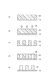
- G2 negative for resolution evaluation: having a wiring pattern with a line width / space width of x / x (x: 30 to 200, unit: ⁇ m)
- No. Number of remaining steps after development of Hitachi 41-step step tablet using 3 negative for resolution evaluation: line width / space width x / x (x: 6 to 47, unit: ⁇ m) wiring pattern
- the exposure was performed with an energy amount of 14.0.
- the PET film was peeled off, and a 1% by mass sodium carbonate aqueous solution at 30 ° C. was sprayed for twice the shortest development time (the shortest time for removing the unexposed portion) to remove the unexposed portion.
- the space portion (unexposed portion) is cleanly removed, and the line portion (exposed portion) is formed without meandering or chipping.
- the resolution was evaluated. The resolution was evaluated by the minimum value of the space width. The smaller this number is, the better the resolution is.
- the copper-clad laminate was changed to an FPC substrate (manufactured by Nikkan Kogyo Co., Ltd., trade name: F-30VC1, substrate thickness: 25 ⁇ m, copper thickness: 18 ⁇ m), and the FPC substrate, photosensitive layer, and PET film were laminated in this order. A laminate was obtained.
- a parallel light exposure device (EXM-1201) is used to expose the photosensitive layer with an energy amount of 14 steps, which is the number of remaining steps after development of the 41-step step tablet. It was cured. Then, the PET film was peeled off and then developed to obtain a flexibility evaluation substrate on which a resist pattern of 10 mm ⁇ 100 mm was formed on the FPC substrate.
- the minimum cylindrical diameter (mm) that did not peel off between the FPC substrate and the resist pattern was determined.
- the diameter of the cylinder was evaluated as 2, 3, 4, 5, 6, 8, 9, 10, 11, 12, 13, 15, 20, 25 and 30 (unit: mm). The smaller the minimum diameter of the cylinder, the better the flexibility.
- the evaluation result was “> 30” when peeling was confirmed between the FPC base material and the resist layer.
- Photosensitive resin film 1 ... Photosensitive resin film, 2 ... Support film, 10 ... Substrate, 20 ... Photosensitive layer, 22 ... Resist pattern, 30 ... Active light rays, 40 ... Plating layer, 42 ... Conductor pattern.
Landscapes
- Physics & Mathematics (AREA)
- General Physics & Mathematics (AREA)
- Chemical & Material Sciences (AREA)
- Spectroscopy & Molecular Physics (AREA)
- Polymers & Plastics (AREA)
- Engineering & Computer Science (AREA)
- Organic Chemistry (AREA)
- Health & Medical Sciences (AREA)
- Chemical Kinetics & Catalysis (AREA)
- Medicinal Chemistry (AREA)
- Manufacturing & Machinery (AREA)
- Microelectronics & Electronic Packaging (AREA)
- Materials Engineering (AREA)
- Materials For Photolithography (AREA)
- Manufacturing Of Printed Wiring (AREA)
- Manufacturing Of Printed Circuit Boards (AREA)
Priority Applications (8)
| Application Number | Priority Date | Filing Date | Title |
|---|---|---|---|
| CN201980101133.9A CN114585974A (zh) | 2019-10-16 | 2019-10-16 | 感光性树脂膜、抗蚀剂图案的形成方法及配线图案的形成方法 |
| JP2021552043A JP7590977B2 (ja) | 2019-10-16 | 2019-10-16 | 感光性樹脂フィルム、レジストパターンの形成方法、及び配線パターンの形成方法 |
| KR1020227008154A KR20220084015A (ko) | 2019-10-16 | 2019-10-16 | 감광성 수지 필름, 레지스트 패턴의 형성 방법, 및 배선 패턴의 형성 방법 |
| MYPI2022000916A MY207705A (en) | 2019-10-16 | 2019-10-16 | Photosensitive resin film, resist pattern forming method, and wiring pattern forming method |
| US17/767,655 US20240111211A1 (en) | 2019-10-16 | 2019-10-16 | Photosensitive resin film, resist pattern forming method, and wiring pattern forming method |
| KR1020257042181A KR20260006056A (ko) | 2019-10-16 | 2019-10-16 | 감광성 수지 필름, 레지스트 패턴의 형성 방법, 및 배선 패턴의 형성 방법 |
| PCT/JP2019/040754 WO2021075005A1 (ja) | 2019-10-16 | 2019-10-16 | 感光性樹脂フィルム、レジストパターンの形成方法、及び配線パターンの形成方法 |
| JP2023188413A JP2024003098A (ja) | 2019-10-16 | 2023-11-02 | 感光性樹脂フィルム、レジストパターンの形成方法、及び配線パターンの形成方法 |
Applications Claiming Priority (1)
| Application Number | Priority Date | Filing Date | Title |
|---|---|---|---|
| PCT/JP2019/040754 WO2021075005A1 (ja) | 2019-10-16 | 2019-10-16 | 感光性樹脂フィルム、レジストパターンの形成方法、及び配線パターンの形成方法 |
Publications (1)
| Publication Number | Publication Date |
|---|---|
| WO2021075005A1 true WO2021075005A1 (ja) | 2021-04-22 |
Family
ID=75537535
Family Applications (1)
| Application Number | Title | Priority Date | Filing Date |
|---|---|---|---|
| PCT/JP2019/040754 Ceased WO2021075005A1 (ja) | 2019-10-16 | 2019-10-16 | 感光性樹脂フィルム、レジストパターンの形成方法、及び配線パターンの形成方法 |
Country Status (6)
| Country | Link |
|---|---|
| US (1) | US20240111211A1 (https=) |
| JP (2) | JP7590977B2 (https=) |
| KR (2) | KR20220084015A (https=) |
| CN (1) | CN114585974A (https=) |
| MY (1) | MY207705A (https=) |
| WO (1) | WO2021075005A1 (https=) |
Cited By (1)
| Publication number | Priority date | Publication date | Assignee | Title |
|---|---|---|---|---|
| WO2024135501A1 (ja) * | 2022-12-19 | 2024-06-27 | 株式会社レゾナック | 感光性エレメント、及び、レジストパターンの形成方法 |
Citations (8)
| Publication number | Priority date | Publication date | Assignee | Title |
|---|---|---|---|---|
| JP2002372781A (ja) * | 2002-05-30 | 2002-12-26 | Hitachi Chem Co Ltd | 感光性エレメント |
| JP2005309273A (ja) * | 2004-04-26 | 2005-11-04 | Tokyo Ohka Kogyo Co Ltd | 感光性樹脂組成物およびこれを用いた感光性ドライフィルム |
| JP2006251386A (ja) * | 2005-03-10 | 2006-09-21 | Fuji Photo Film Co Ltd | 永久パターン形成方法 |
| JP2009020191A (ja) * | 2007-07-10 | 2009-01-29 | Hitachi Chem Co Ltd | 感光性樹脂組成物及び感光性フィルム |
| JP2012215676A (ja) * | 2011-03-31 | 2012-11-08 | Asahi Kasei E-Materials Corp | 感光性樹脂組成物及びそれを用いた積層体 |
| JP2013200328A (ja) * | 2012-03-23 | 2013-10-03 | Toray Ind Inc | 感光性樹脂組成物およびそれからなるフィルム積層体 |
| WO2013172302A1 (ja) * | 2012-05-14 | 2013-11-21 | 日立化成株式会社 | 感光性樹脂組成物、感光性エレメント、画像表示装置の隔壁の形成方法、画像表示装置の製造方法及び画像表示装置 |
| WO2018173840A1 (ja) * | 2017-03-21 | 2018-09-27 | 東レ株式会社 | 感光性樹脂組成物、感光性樹脂組成物フィルム、絶縁膜および電子部品 |
Family Cites Families (19)
| Publication number | Priority date | Publication date | Assignee | Title |
|---|---|---|---|---|
| GB2135326B (en) * | 1982-12-20 | 1986-09-03 | Fuji Photo Film Co Ltd | Photopolymerizable compositions having improved adhesive to metal surfaces |
| JP4108243B2 (ja) | 1999-04-14 | 2008-06-25 | 旭化成エレクトロニクス株式会社 | 感光性樹脂積層体 |
| JP2002258475A (ja) * | 2001-03-01 | 2002-09-11 | Hitachi Chem Co Ltd | 感光性樹脂組成物、これを用いた感光性エレメント、レジストパターンの形成方法及び半導体パッケージ用回路基板の製造方法 |
| JP2006244931A (ja) * | 2005-03-04 | 2006-09-14 | Fuji Photo Film Co Ltd | プラズマディスプレイパネル用隔壁の製造方法 |
| KR100934046B1 (ko) * | 2005-05-23 | 2009-12-24 | 히다치 가세고교 가부시끼가이샤 | 감광성 수지 조성물, 감광성 엘리먼트, 레지스트 패턴의 형성방법 및 프린트 배선판의 제조방법 |
| JP4761909B2 (ja) * | 2005-10-05 | 2011-08-31 | 旭化成イーマテリアルズ株式会社 | 感光性樹脂組成物及び積層体 |
| DE102006056073A1 (de) | 2006-11-28 | 2008-05-29 | Arvinmeritor Emissions Technologies Gmbh | Krümmer für eine Abgasanlage |
| MY152732A (en) * | 2008-04-28 | 2014-11-28 | Hitachi Chemical Co Ltd | Photosensitive resin composition, photosensitive element, method for forming resist pattern and method for manufacturing printed wiring board |
| JP2010091662A (ja) * | 2008-10-06 | 2010-04-22 | Hitachi Chem Co Ltd | 感光性樹脂組成物、並びにこれを用いた感光性エレメント、レジストパターンの製造法及びプリント配線板の製造法 |
| CN103543608A (zh) * | 2009-02-26 | 2014-01-29 | 日立化成工业株式会社 | 感光性树脂组合物、以及使用了该组合物的感光性元件、抗蚀剂图案的形成方法和印刷线路板的制造方法 |
| JP5768521B2 (ja) * | 2010-07-13 | 2015-08-26 | 日立化成株式会社 | 感光性エレメント、それを用いたレジストパターンの形成方法及びプリント配線板の製造方法 |
| KR101444044B1 (ko) * | 2010-12-16 | 2014-09-23 | 히타치가세이가부시끼가이샤 | 감광성 엘리먼트, 레지스트 패턴의 형성 방법 및 프린트 배선판의 제조 방법 |
| JP5935462B2 (ja) * | 2011-05-10 | 2016-06-15 | 日立化成株式会社 | 感光性エレメント、レジストパターンの形成方法、プリント配線板の製造方法 |
| KR102281035B1 (ko) * | 2012-11-20 | 2021-07-22 | 쇼와덴코머티리얼즈가부시끼가이샤 | 감광성 수지 조성물, 감광성 엘리먼트, 레지스터 패턴의 형성 방법 및 프린트 배선판의 제조 방법 |
| CN105393171B (zh) * | 2013-07-23 | 2019-11-26 | 日立化成株式会社 | 投影曝光用感光性树脂组合物、感光性元件、抗蚀图案的形成方法、印刷配线板的制造方法和引线框的制造方法 |
| JPWO2016104585A1 (ja) * | 2014-12-25 | 2017-10-05 | 日立化成株式会社 | 感光性樹脂組成物、並びにこれを用いた感光性エレメント、レジストパターンの形成方法、及びプリント配線板の製造方法 |
| JP6782417B2 (ja) | 2015-07-29 | 2020-11-11 | 昭和電工マテリアルズ株式会社 | 感光性樹脂組成物、感光性エレメント、レジストパターンの形成方法及びプリント配線板の製造方法 |
| MY196431A (en) * | 2015-07-30 | 2023-04-10 | Hitachi Chemical Co Ltd | Photosensitive Element, Resin Composition For Forming Barrier Layer, Method For Forming Resist Pattern, And Method For Producing Printed Wiring Board |
| WO2017169574A1 (ja) * | 2016-03-30 | 2017-10-05 | 東レ株式会社 | 感光性接着剤組成物、硬化物、感光性接着剤シート、積層基板および接着剤パターン付積層基板の製造方法 |
-
2019
- 2019-10-16 KR KR1020227008154A patent/KR20220084015A/ko not_active Ceased
- 2019-10-16 US US17/767,655 patent/US20240111211A1/en active Pending
- 2019-10-16 JP JP2021552043A patent/JP7590977B2/ja active Active
- 2019-10-16 WO PCT/JP2019/040754 patent/WO2021075005A1/ja not_active Ceased
- 2019-10-16 MY MYPI2022000916A patent/MY207705A/en unknown
- 2019-10-16 CN CN201980101133.9A patent/CN114585974A/zh active Pending
- 2019-10-16 KR KR1020257042181A patent/KR20260006056A/ko active Pending
-
2023
- 2023-11-02 JP JP2023188413A patent/JP2024003098A/ja active Pending
Patent Citations (8)
| Publication number | Priority date | Publication date | Assignee | Title |
|---|---|---|---|---|
| JP2002372781A (ja) * | 2002-05-30 | 2002-12-26 | Hitachi Chem Co Ltd | 感光性エレメント |
| JP2005309273A (ja) * | 2004-04-26 | 2005-11-04 | Tokyo Ohka Kogyo Co Ltd | 感光性樹脂組成物およびこれを用いた感光性ドライフィルム |
| JP2006251386A (ja) * | 2005-03-10 | 2006-09-21 | Fuji Photo Film Co Ltd | 永久パターン形成方法 |
| JP2009020191A (ja) * | 2007-07-10 | 2009-01-29 | Hitachi Chem Co Ltd | 感光性樹脂組成物及び感光性フィルム |
| JP2012215676A (ja) * | 2011-03-31 | 2012-11-08 | Asahi Kasei E-Materials Corp | 感光性樹脂組成物及びそれを用いた積層体 |
| JP2013200328A (ja) * | 2012-03-23 | 2013-10-03 | Toray Ind Inc | 感光性樹脂組成物およびそれからなるフィルム積層体 |
| WO2013172302A1 (ja) * | 2012-05-14 | 2013-11-21 | 日立化成株式会社 | 感光性樹脂組成物、感光性エレメント、画像表示装置の隔壁の形成方法、画像表示装置の製造方法及び画像表示装置 |
| WO2018173840A1 (ja) * | 2017-03-21 | 2018-09-27 | 東レ株式会社 | 感光性樹脂組成物、感光性樹脂組成物フィルム、絶縁膜および電子部品 |
Cited By (1)
| Publication number | Priority date | Publication date | Assignee | Title |
|---|---|---|---|---|
| WO2024135501A1 (ja) * | 2022-12-19 | 2024-06-27 | 株式会社レゾナック | 感光性エレメント、及び、レジストパターンの形成方法 |
Also Published As
| Publication number | Publication date |
|---|---|
| JP7590977B2 (ja) | 2024-11-27 |
| JP2024003098A (ja) | 2024-01-11 |
| JPWO2021075005A1 (https=) | 2021-04-22 |
| CN114585974A (zh) | 2022-06-03 |
| KR20260006056A (ko) | 2026-01-12 |
| KR20220084015A (ko) | 2022-06-21 |
| US20240111211A1 (en) | 2024-04-04 |
| MY207705A (en) | 2025-03-13 |
Similar Documents
| Publication | Publication Date | Title |
|---|---|---|
| JP5618118B2 (ja) | 感光性樹脂組成物,並びにこれを用いた感光性エレメント,ソルダーレジスト及びプリント配線板 | |
| TWI689783B (zh) | 感光性樹脂組成物、感光性元件、抗蝕劑圖案的形成方法以及印刷電路板的製造方法 | |
| JP5626428B2 (ja) | 感光性樹脂組成物、並びにこれを用いた感光性エレメント、レジストパターンの形成方法及びプリント配線板の製造方法 | |
| JP5729495B2 (ja) | 感光性樹脂組成物を用いた感光性エレメント、ソルダーレジスト及びプリント配線板 | |
| WO2010098183A1 (ja) | 感光性樹脂組成物、並びにこれを用いた感光性エレメント、レジストパターンの形成方法及びプリント配線板の製造方法 | |
| JPWO2007123062A1 (ja) | 感光性エレメント、レジストパターンの形成方法及びプリント配線板の製造方法 | |
| CN102007451A (zh) | 感光性树脂组合物、感光性元件、抗蚀图形的形成方法及印刷电路板的制造方法 | |
| JP5600903B2 (ja) | 感光性樹脂組成物、並びにこれを用いた感光性エレメント、レジストパターンの形成方法及びプリント配線板の製造方法 | |
| JP2024008940A (ja) | 感光性樹脂組成物、感光性エレメント、レジストパターンの形成方法及びプリント配線板の製造方法 | |
| WO2021152709A1 (ja) | 感光性エレメント、レジストパターンの形成方法及びプリント配線板の製造方法 | |
| JP2024003098A (ja) | 感光性樹脂フィルム、レジストパターンの形成方法、及び配線パターンの形成方法 | |
| JP7631907B2 (ja) | 感光性樹脂フィルム、感光性エレメント、及び、積層体の製造方法 | |
| JP7816574B2 (ja) | 感光性樹脂組成物、感光性エレメント、及び配線基板の製造方法 | |
| JP7327485B2 (ja) | 感光性樹脂組成物、感光性エレメント、レジストパターンの形成方法及びプリント配線板の製造方法 | |
| JP3634216B2 (ja) | 感光性樹脂組成物、これを用いた感光性エレメント、レジストパターンの製造法及びプリント配線板の製造法 | |
| JP2004279479A (ja) | 感光性エレメント、これを用いたレジストパターンの形成方法及びプリント配線板の製造方法 | |
| JP2005257812A (ja) | 感光性樹脂組成物、これを用いた感光性エレメント、レジストパターンの形成方法及びプリント配線板の製造方法 | |
| WO2024135501A1 (ja) | 感光性エレメント、及び、レジストパターンの形成方法 | |
| WO2022201432A1 (ja) | 感光性樹脂フィルム、レジストパターンの形成方法、及び配線パターンの形成方法 | |
| WO2024142486A1 (ja) | 感光性エレメント及び配線基板の製造方法 | |
| WO2025115820A1 (ja) | 感光性樹脂組成物、感光性エレメント、レジストパターンの形成方法及びプリント配線板の製造方法 | |
| WO2025220085A1 (ja) | 感光性エレメント、レジストパターンの形成方法、及び配線基板の製造方法 | |
| WO2025127002A1 (ja) | 感光性樹脂組成物、感光性エレメント、レジストパターンの形成方法及びプリント配線板の製造方法 | |
| WO2026042140A1 (ja) | 感光性エレメント、レジストパターンの形成方法、及びプリント配線板の製造方法 | |
| WO2022264275A1 (ja) | 感光性エレメント及び感光性エレメントの製造方法 |
Legal Events
| Date | Code | Title | Description |
|---|---|---|---|
| 121 | Ep: the epo has been informed by wipo that ep was designated in this application |
Ref document number: 19949500 Country of ref document: EP Kind code of ref document: A1 |
|
| ENP | Entry into the national phase |
Ref document number: 2021552043 Country of ref document: JP Kind code of ref document: A |
|
| WWE | Wipo information: entry into national phase |
Ref document number: 17767655 Country of ref document: US |
|
| NENP | Non-entry into the national phase |
Ref country code: DE |
|
| 32PN | Ep: public notification in the ep bulletin as address of the adressee cannot be established |
Free format text: NOTING OF LOSS OF RIGHTS PURSUANT TO RULE 112(1) EPC (EPO FORM 1205A DATED 28/07/2022) |
|
| 122 | Ep: pct application non-entry in european phase |
Ref document number: 19949500 Country of ref document: EP Kind code of ref document: A1 |
|
| WWR | Wipo information: refused in national office |
Ref document number: 1020227008154 Country of ref document: KR |
|
| WWC | Wipo information: continuation of processing after refusal or withdrawal |
Ref document number: 1020227008154 Country of ref document: KR |